Embed Size (px)
Citation preview

Lecture 10ANNOUNCEMENTS
• Alan Wu will hold an extra lab session tomorrow (9/28), 2‐4PMAlan Wu will hold an extra lab session tomorrow (9/28), 2 4PM• The post‐lab assignment for Experiment #4 has been shortened!• 2 pgs of notes (double‐sided, 8.5”×11”) allowed for Midterm #1
OUTLINE• BJT Amplifiers (cont’d)
CB t ith bi i– CB stage with biasing– Emitter follower (Common‐collector amplifier)
– Analysis of emitter follower core– Impact of source resistance– Impact of Early effect– Emitter follower with biasing
EE105 Fall 2007 Lecture 10, Slide 1 Prof. Liu, UC Berkeley
Emitter follower with biasing
Reading: Chapter 5.3.3‐5.4
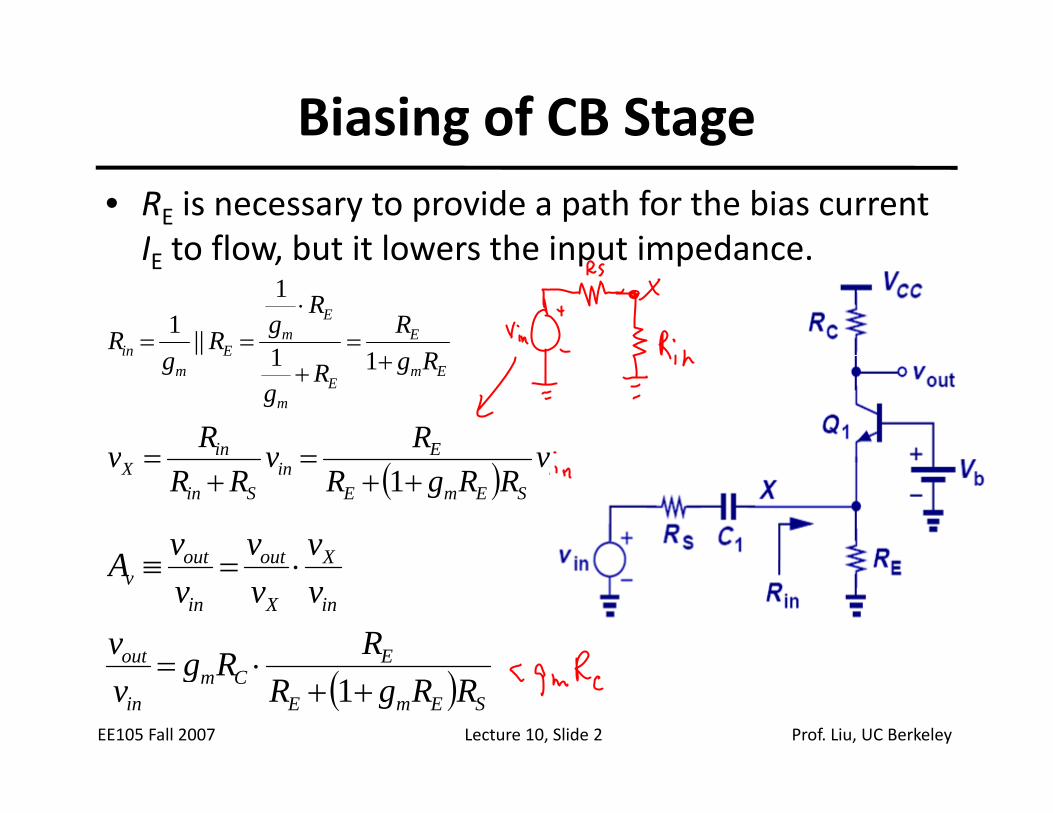
Biasing of CB Stage• RE is necessary to provide a path for the bias current I to flow but it lowers the input impedanceIE to flow, but it lowers the input impedance.
EE
mEin R
RR
gRR =⋅
==11
1
||1
Ein vRvRv ==
EmE
m
Em
in RgRg
g ++ 11
Xoutout vvvA
( ) inSEmE
inSin
X vRRgR
vRR
v++
=+
=1
Eout
in
X
X
out
in
outv
RRgvvvv
A
=
⋅=≡
EE105 Fall 2007 Lecture 10, Slide 2 Prof. Liu, UC Berkeley
( ) SEmECm
in RRgRRg
v ++⋅=
1
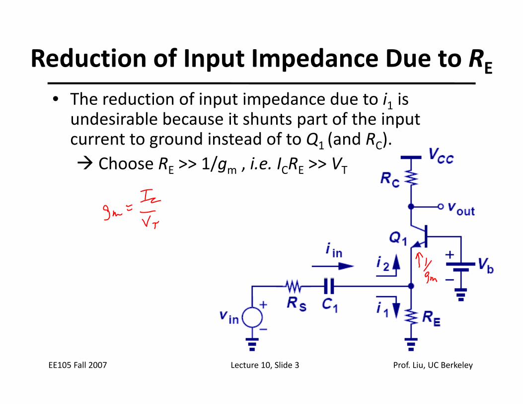
Reduction of Input Impedance Due to RE
• The reduction of input impedance due to i1 is undesirable because it shunts part of the input p pcurrent to ground instead of to Q1 (and RC).
Choose RE >> 1/gm , i.e. ICRE >> VT
EE105 Fall 2007 Lecture 10, Slide 3 Prof. Liu, UC Berkeley
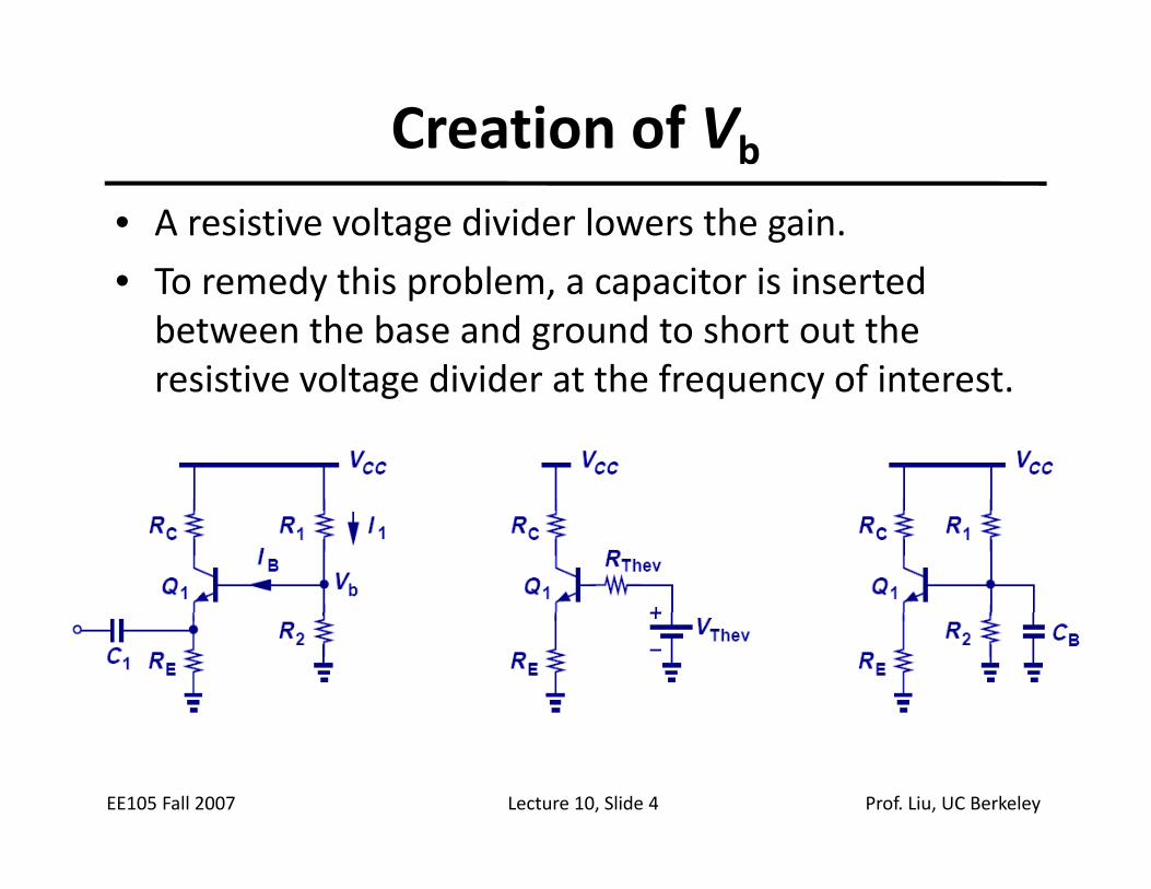
Creation of Vb
• A resistive voltage divider lowers the gain.
• To remedy this problem a capacitor is inserted• To remedy this problem, a capacitor is inserted between the base and ground to short out the resistive voltage divider at the frequency of interest.resistive voltage divider at the frequency of interest.
EE105 Fall 2007 Lecture 10, Slide 4 Prof. Liu, UC Berkeley
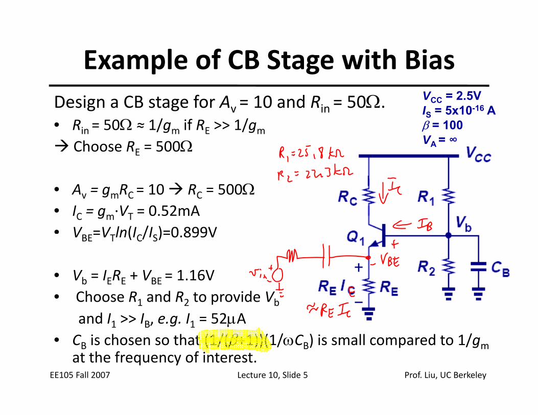
Example of CB Stage with Bias Design a CB stage for Av = 10 and Rin = 50Ω.• Rin = 50Ω ≈ 1/gm if RE >> 1/gm
VCC = 2.5VIS = 5x10-16 Aβ = 100Rin 50Ω 1/gm if RE >> 1/gm
Choose RE = 500Ωβ 100VA = ∞
• Av = gmRC = 10 RC = 500Ω• IC = gm∙VT = 0.52mA• V =V ln(I /I )=0 899VVBE=VTln(IC/IS)=0.899V
• Vb = IERE + VBE = 1.16V• Choose R1 and R2 to provide Vb
and I1 >> IB, e.g. I1 = 52µA• C is chosen so that (1/(β+1))(1/ωC ) is small compared to 1/g
EE105 Fall 2007 Lecture 10, Slide 5 Prof. Liu, UC Berkeley
• CB is chosen so that (1/(β+1))(1/ωCB) is small compared to 1/gmat the frequency of interest.
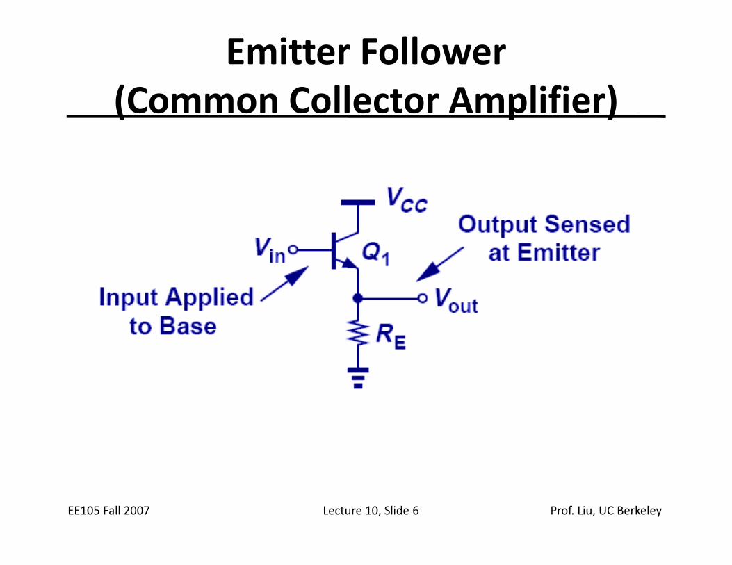
Emitter Follower (Common Collector Amplifier)(Common Collector Amplifier)
EE105 Fall 2007 Lecture 10, Slide 6 Prof. Liu, UC Berkeley
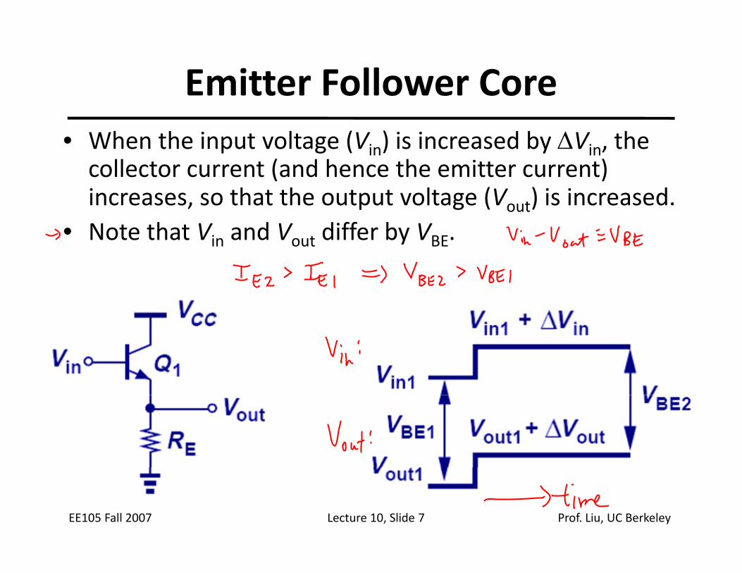
Emitter Follower Core• When the input voltage (Vin) is increased by ∆Vin, the collector current (and hence the emitter current) ( )increases, so that the output voltage (Vout) is increased.
• Note that Vin and Vout differ by VBE.
EE105 Fall 2007 Lecture 10, Slide 7 Prof. Liu, UC Berkeley
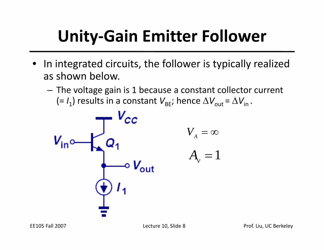
Unity‐Gain Emitter Follower• In integrated circuits, the follower is typically realized as shown belowas shown below.– The voltage gain is 1 because a constant collector current (= I1) results in a constant VBE; hence ∆Vout = ∆Vin .
∞=AV
1=vA
EE105 Fall 2007 Lecture 10, Slide 8 Prof. Liu, UC Berkeley
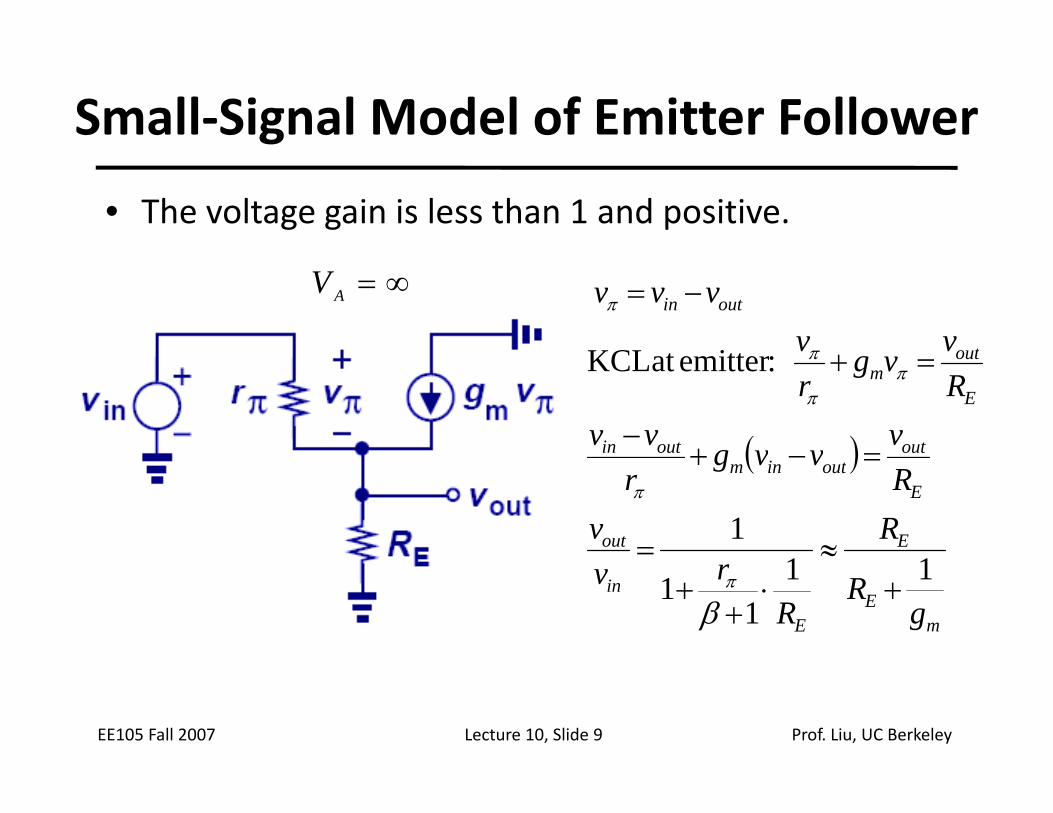
Small‐Signal Model of Emitter Follower
• The voltage gain is less than 1 and positive.
out
outin
vvvvv
itttKCL
+
−=
π
π∞=AV
( ) outoutin
E
outm
vvvgvvR
vgr
:emitterat KCL
=−+−
=+ ππ
π
( )
Eout
Eoutinm
RvR
vvgr
111
≈=
=+π
mE
E
in
gR
Rrv 11
11 +⋅
++
βπ
EE105 Fall 2007 Lecture 10, Slide 9 Prof. Liu, UC Berkeley
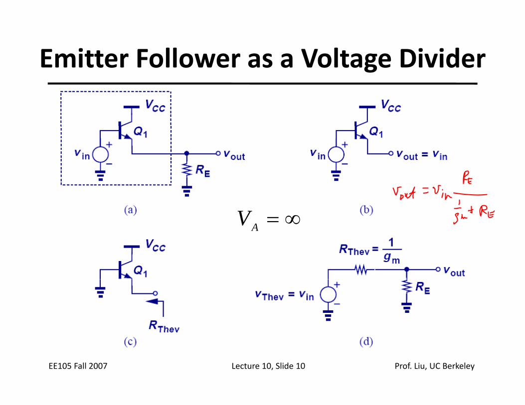
Emitter Follower as a Voltage Divider
∞=AVA
EE105 Fall 2007 Lecture 10, Slide 10 Prof. Liu, UC Berkeley
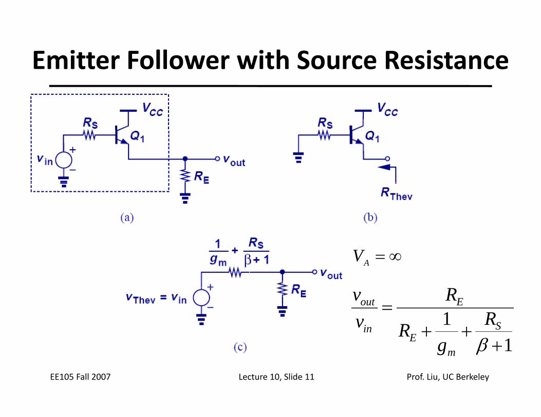
Emitter Follower with Source Resistance
∞=AV
11
++=
βS
E
E
in
out
RR
Rvv
EE105 Fall 2007 Lecture 10, Slide 11 Prof. Liu, UC Berkeley
1+βmE g
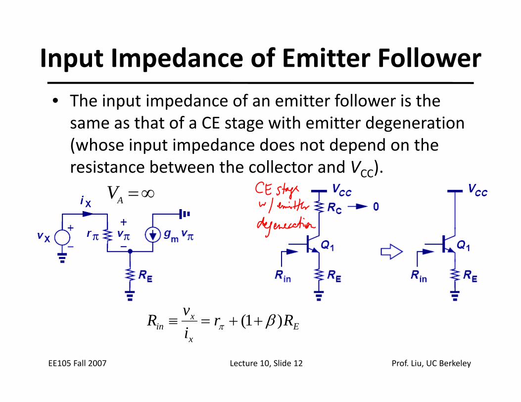
Input Impedance of Emitter Follower• The input impedance of an emitter follower is the same as that of a CE stage with emitter degenerationsame as that of a CE stage with emitter degeneration (whose input impedance does not depend on the resistance between the collector and VCC).CC)
∞=AV
Ex
in RrivR )1( βπ ++=≡
EE105 Fall 2007 Lecture 10, Slide 12 Prof. Liu, UC Berkeley
Ex
in i)( βπ
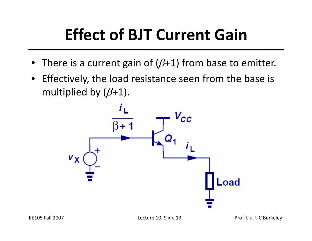
Effect of BJT Current Gain
• There is a current gain of (β+1) from base to emitter.ff i l h l d i f h b i• Effectively, the load resistance seen from the base is multiplied by (β+1).
EE105 Fall 2007 Lecture 10, Slide 13 Prof. Liu, UC Berkeley
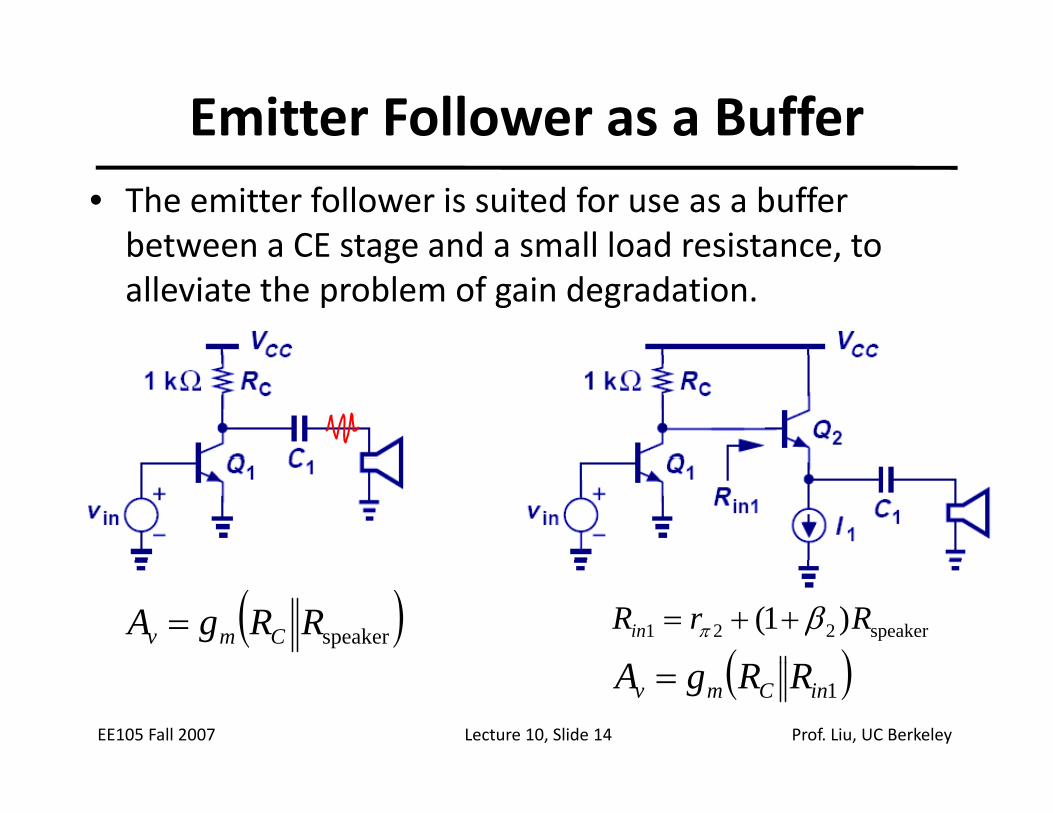
Emitter Follower as a Buffer • The emitter follower is suited for use as a buffer between a CE stage and a small load resistance, tobetween a CE stage and a small load resistance, to alleviate the problem of gain degradation.
speaker221 )1( RrRin βπ ++=
( )A( )speakerRRgA Cmv =
EE105 Fall 2007 Lecture 10, Slide 14 Prof. Liu, UC Berkeley
( )1inCmv RRgA =
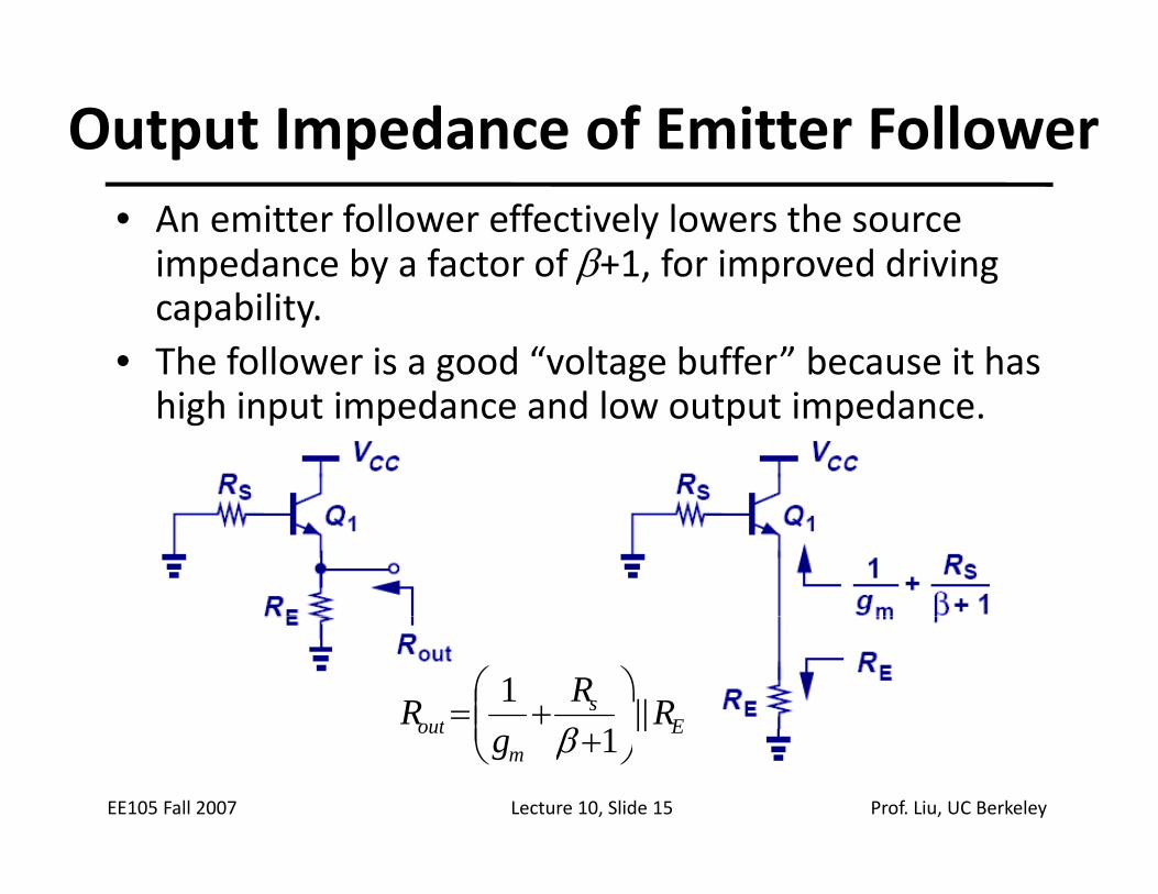
Output Impedance of Emitter Follower• An emitter follower effectively lowers the source impedance by a factor of β+1, for improved driving p y β , p gcapability.
• The follower is a good “voltage buffer” because it has h h d d l dhigh input impedance and low output impedance.
Es
out RRR ||1
1
⎠
⎞⎜⎜⎝
⎛+=
β
EE105 Fall 2007 Lecture 10, Slide 15 Prof. Liu, UC Berkeley
Em
out g||
1⎠⎜⎝ +β
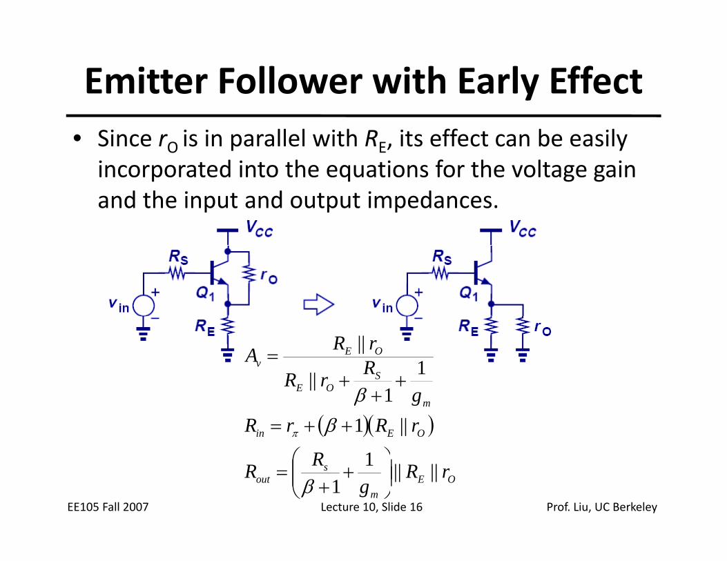
Emitter Follower with Early Effect• Since rO is in parallel with RE, its effect can be easily incorporated into the equations for the voltage gainincorporated into the equations for the voltage gain and the input and output impedances.
SOE
OEv RrR
rRA 1||
||
++=
( )( )OEin
mOE
R
rRrRg
1
||11
||
⎞⎛
++=+
ββ
π
EE105 Fall 2007 Lecture 10, Slide 16 Prof. Liu, UC Berkeley
OEm
sout rR
gRR ||||1
1 ⎟⎟⎠
⎞⎜⎜⎝
⎛+
+=
β
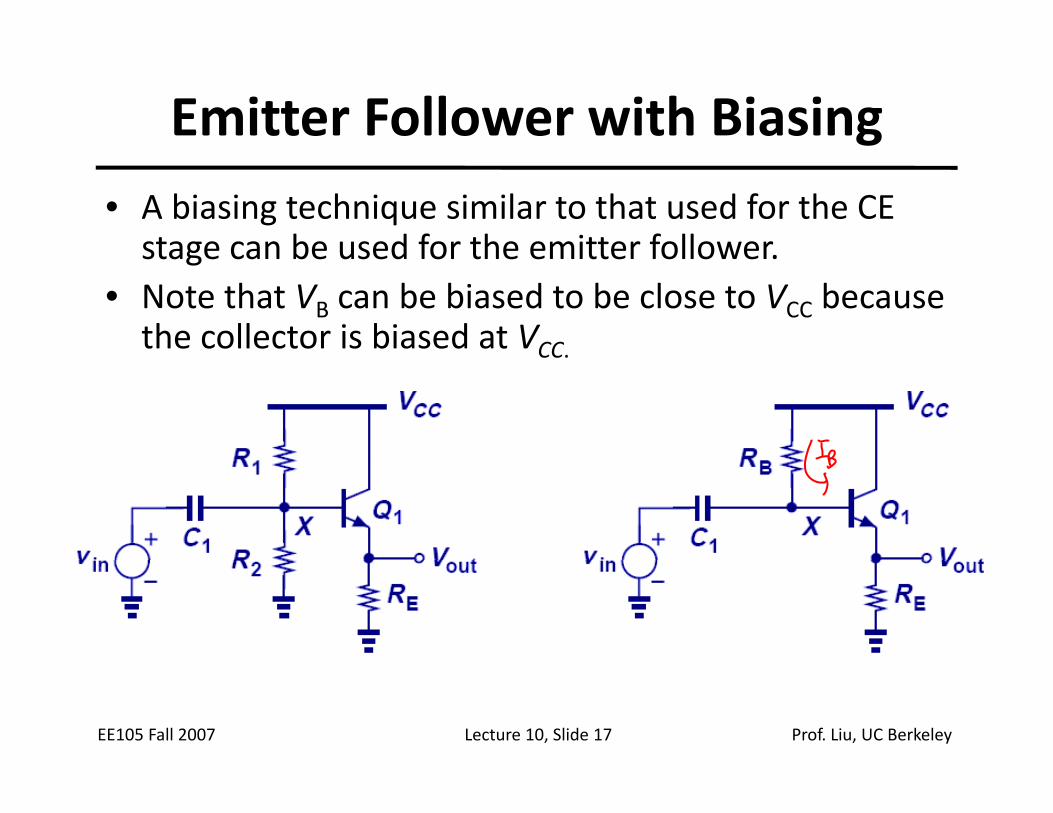
Emitter Follower with Biasing• A biasing technique similar to that used for the CE stage can be used for the emitter followerstage can be used for the emitter follower.
• Note that VB can be biased to be close to VCC because the collector is biased at VCC.CC.
EE105 Fall 2007 Lecture 10, Slide 17 Prof. Liu, UC Berkeley
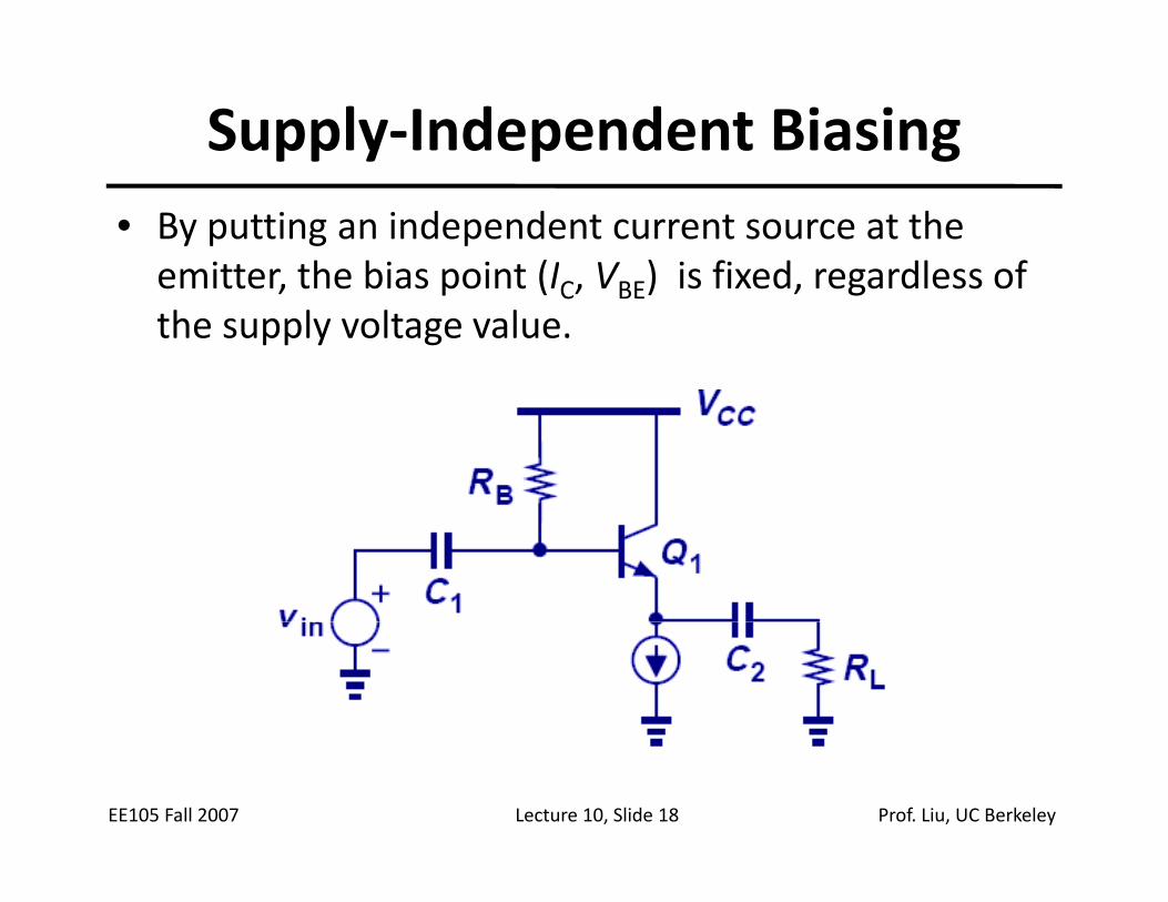
Supply‐Independent Biasing• By putting an independent current source at the emitter the bias point (I V ) is fixed regardless ofemitter, the bias point (IC, VBE) is fixed, regardless of the supply voltage value.
EE105 Fall 2007 Lecture 10, Slide 18 Prof. Liu, UC Berkeley
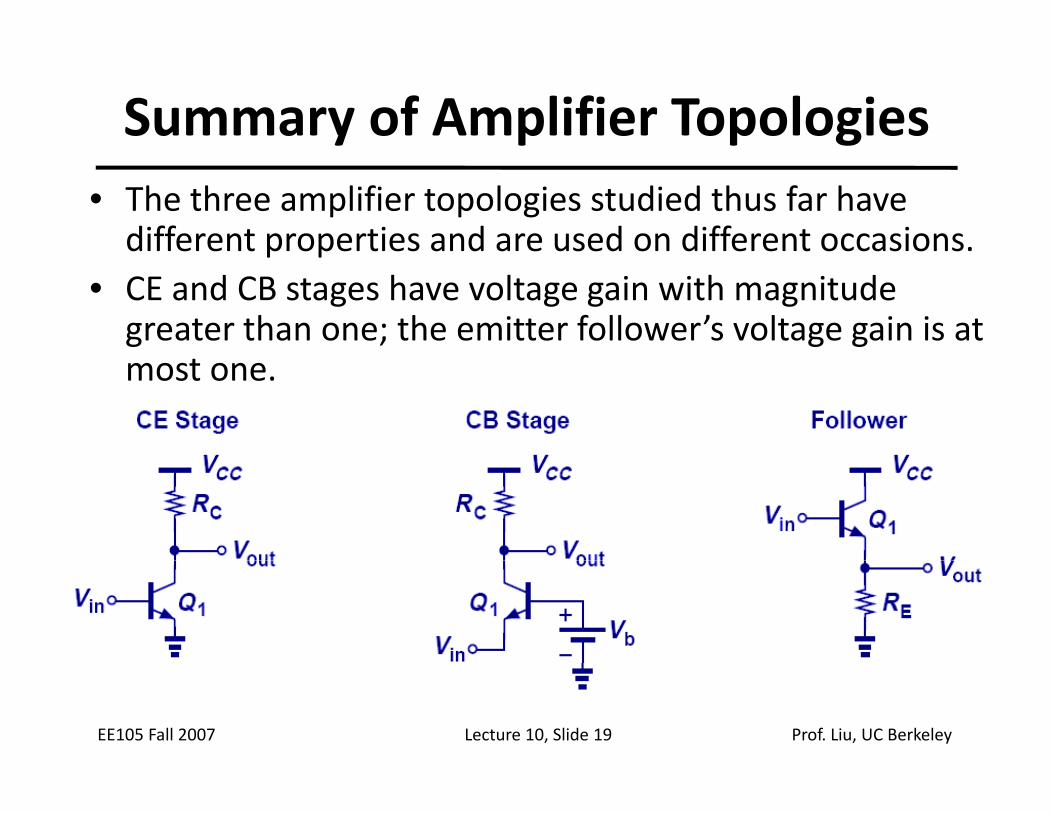
Summary of Amplifier Topologies• The three amplifier topologies studied thus far have different properties and are used on different occasions. p p
• CE and CB stages have voltage gain with magnitude greater than one; the emitter follower’s voltage gain is at most one.
EE105 Fall 2007 Lecture 10, Slide 19 Prof. Liu, UC Berkeley
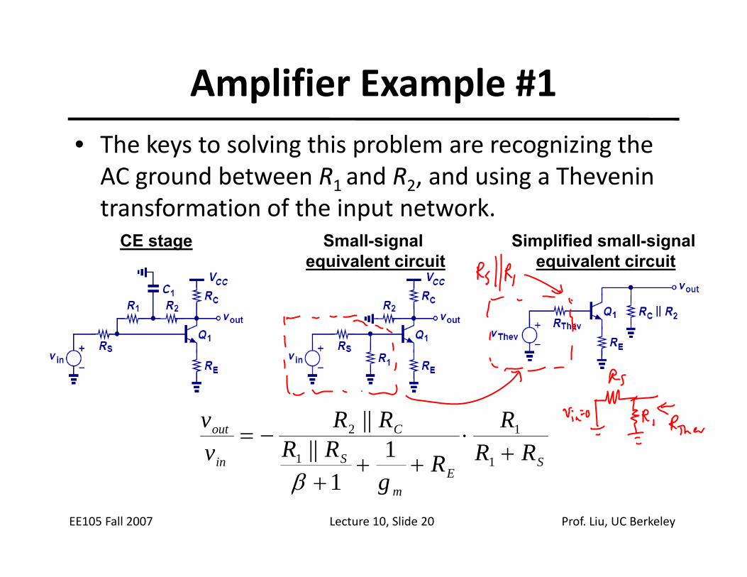
Amplifier Example #1• The keys to solving this problem are recognizing the AC ground between R and R and using a TheveninAC ground between R1 and R2, and using a Thevenin transformation of the input network.
CE stage Small-signal Simplified small-signal equivalent circuit equivalent circuit
SE
S
C
in
out
RRR
RRRRR
vv
+⋅
++−=
1
1
1
2
1||||
EE105 Fall 2007 Lecture 10, Slide 20 Prof. Liu, UC Berkeley
Em
Rg
+++ 1β
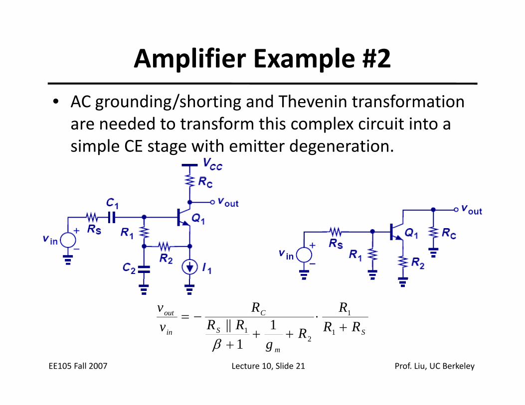
Amplifier Example #2• AC grounding/shorting and Thevenin transformation are needed to transform this complex circuit into aare needed to transform this complex circuit into a simple CE stage with emitter degeneration.
SS
C
i
out
RRR
RRRR
vv
+⋅−=
1
1
1 1||
EE105 Fall 2007 Lecture 10, Slide 21 Prof. Liu, UC Berkeley
S
m
Sin RRRg
v ++++
12
1
1||
β
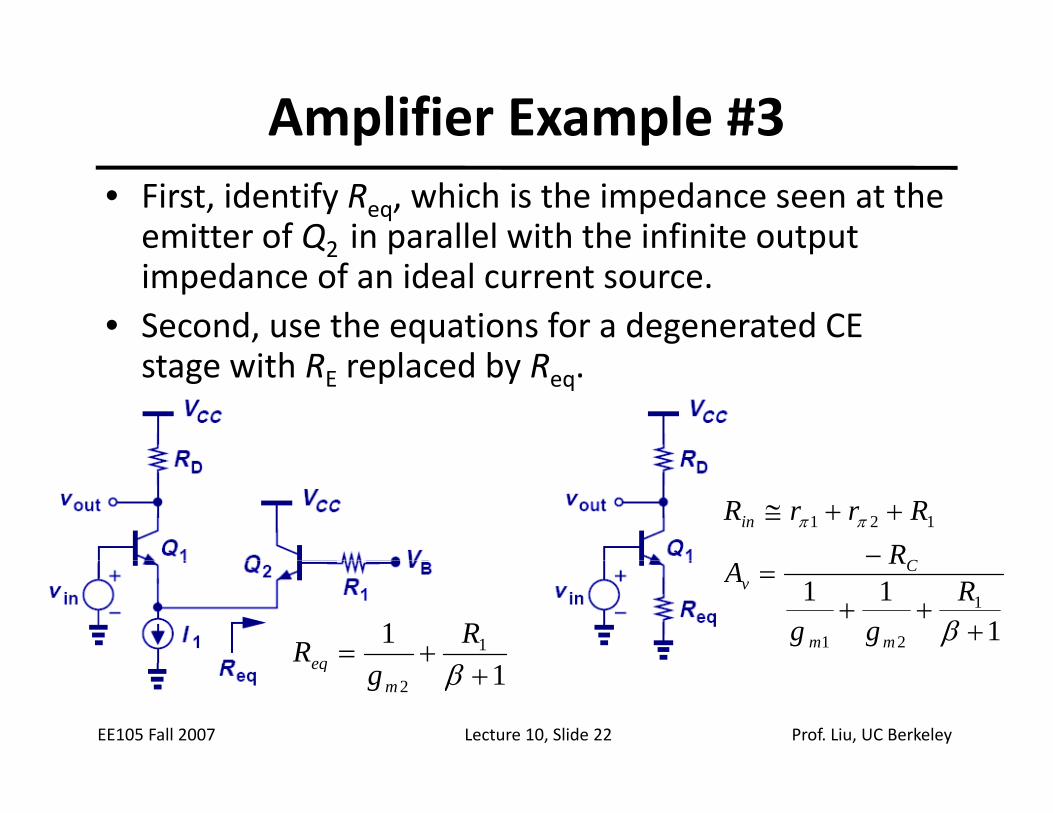
Amplifier Example #3• First, identify Req, which is the impedance seen at the emitter of Q2 in parallel with the infinite output 2 p pimpedance of an ideal current source.
• Second, use the equations for a degenerated CE i h R l d b Rstage with RE replaced by Req.
121
−++≅ ππ
RRrrR
C
in
1 1+=RReq
111 1
21 +++
=
βR
gg
RA
mm
Cv
EE105 Fall 2007 Lecture 10, Slide 22 Prof. Liu, UC Berkeley
12 +βgmeq
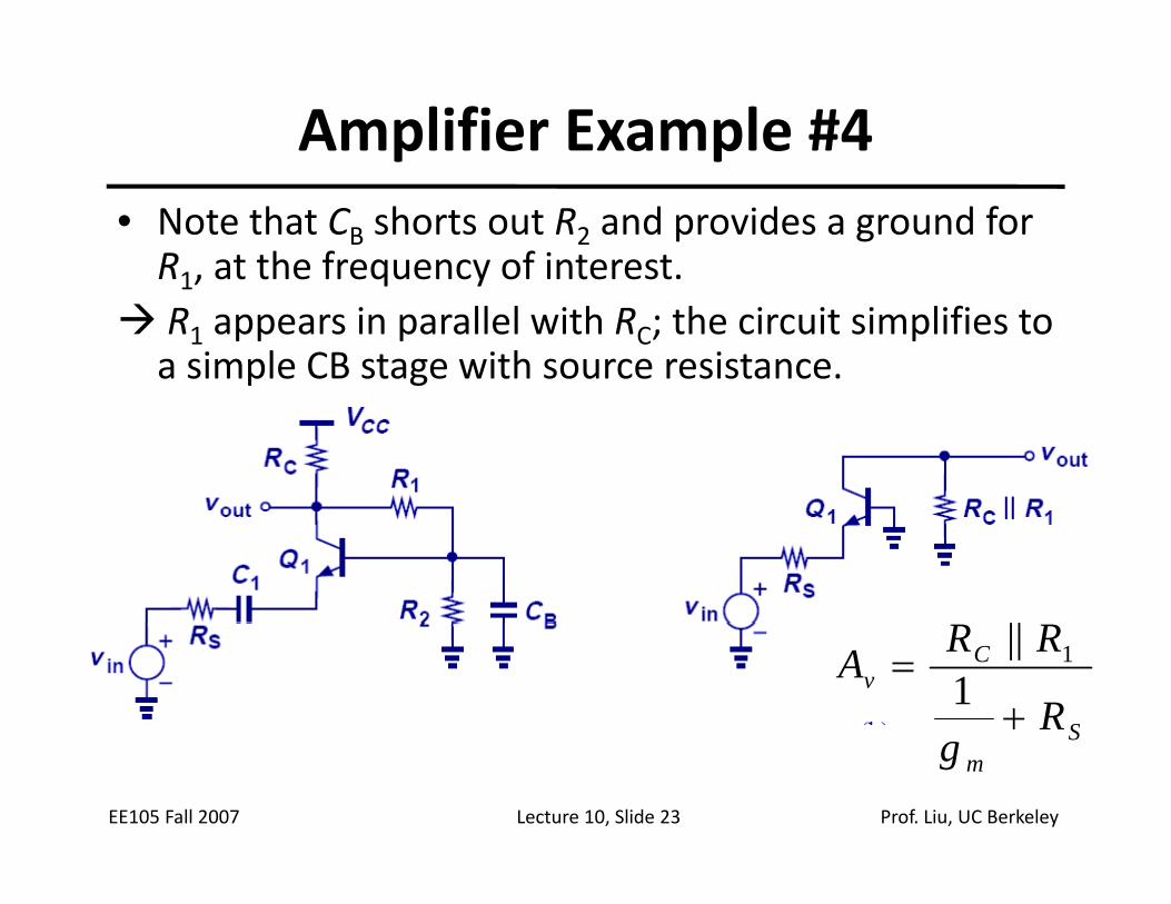
Amplifier Example #4• Note that CB shorts out R2 and provides a ground for R1, at the frequency of interest.1, q yR1 appears in parallel with RC; the circuit simplifies to a simple CB stage with source resistance.
||
S
Cv
R
RRA+
= 1|| 1
EE105 Fall 2007 Lecture 10, Slide 23 Prof. Liu, UC Berkeley
Smg
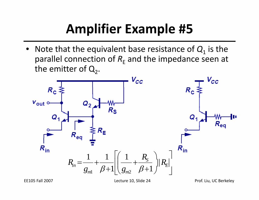
Amplifier Example #5• Note that the equivalent base resistance of Q1 is the parallel connection of RE and the impedance seen at p E pthe emitter of Q2.
⎥⎤
⎢⎡ ⎞⎜⎜⎛
++= S RRR ||111
EE105 Fall 2007 Lecture 10, Slide 24 Prof. Liu, UC Berkeley
⎥⎦
⎢⎣ ⎠⎜⎜⎝ +
++
+= Emm
in Rgg
R ||11 21 ββ