Embed Size (px)
Citation preview
Applied Physics 298r 1 E. Chen (4-12-2004)
Introduction to Nanofabrication
Erli Chen
Center for Imaging and Mesoscale StructureHarvard University
Applied Physics 298r 2 E. Chen (4-12-2004)
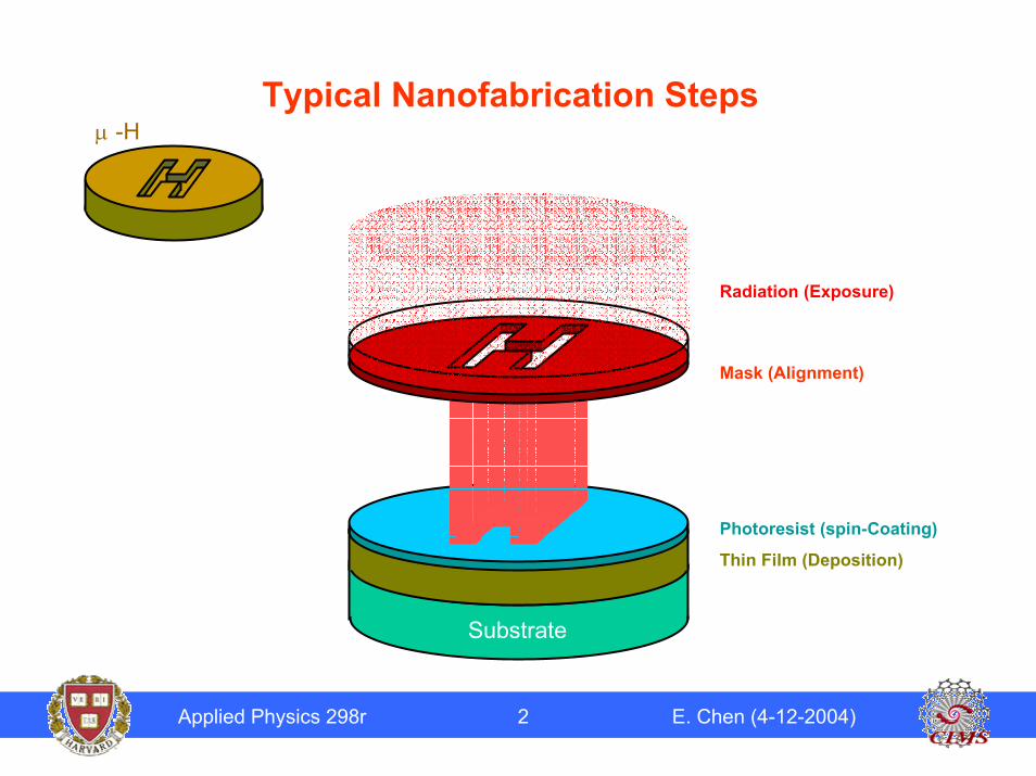
Typical Nanofabrication Steps µ -H
Substrate
Radiation (Exposure)
Mask (Alignment)
Photoresist (spin-Coating)
Thin Film (Deposition)
Applied Physics 298r 3 E. Chen (4-12-2004)
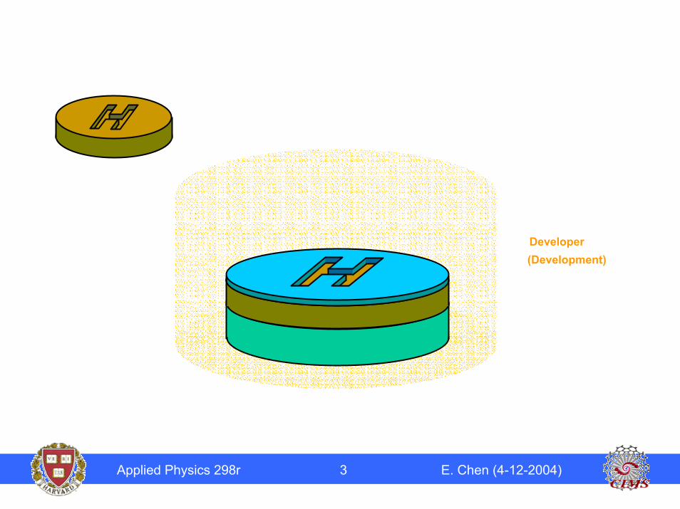
Developer(Development)
Applied Physics 298r 4 E. Chen (4-12-2004)
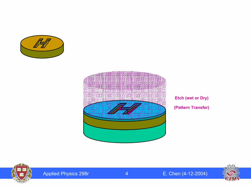
Etch (wet or Dry)
(Pattern Transfer)
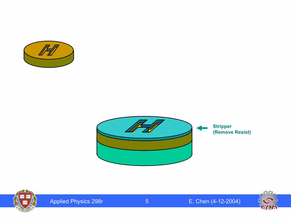
Applied Physics 298r 5 E. Chen (4-12-2004)
Stripper(Remove Resist)
Applied Physics 298r 6 E. Chen (4-12-2004)
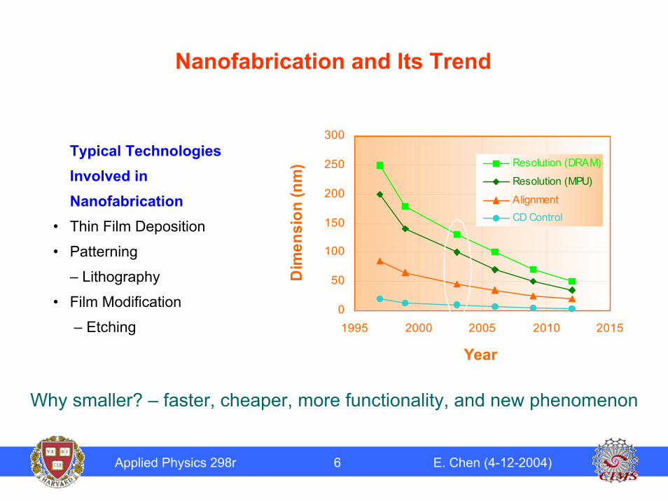
Nanofabrication and Its Trend
0
50
100
150
200
250
300
1995 2000 2005 2010 2015
Year
Dim
ensi
on (n
m) Resolution (DRAM)
Resolution (MPU)
AlignmentCD Control
Typical Technologies Involved in Nanofabrication
• Thin Film Deposition
• Patterning
– Lithography
• Film Modification
– Etching
Why smaller? – faster, cheaper, more functionality, and new phenomenon
Applied Physics 298r 7 E. Chen (4-12-2004)
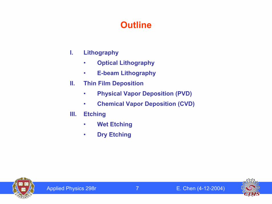
Outline
I. Lithography• Optical Lithography• E-beam Lithography
II. Thin Film Deposition• Physical Vapor Deposition (PVD)• Chemical Vapor Deposition (CVD)
III. Etching• Wet Etching• Dry Etching
Applied Physics 298r 8 E. Chen (4-12-2004)
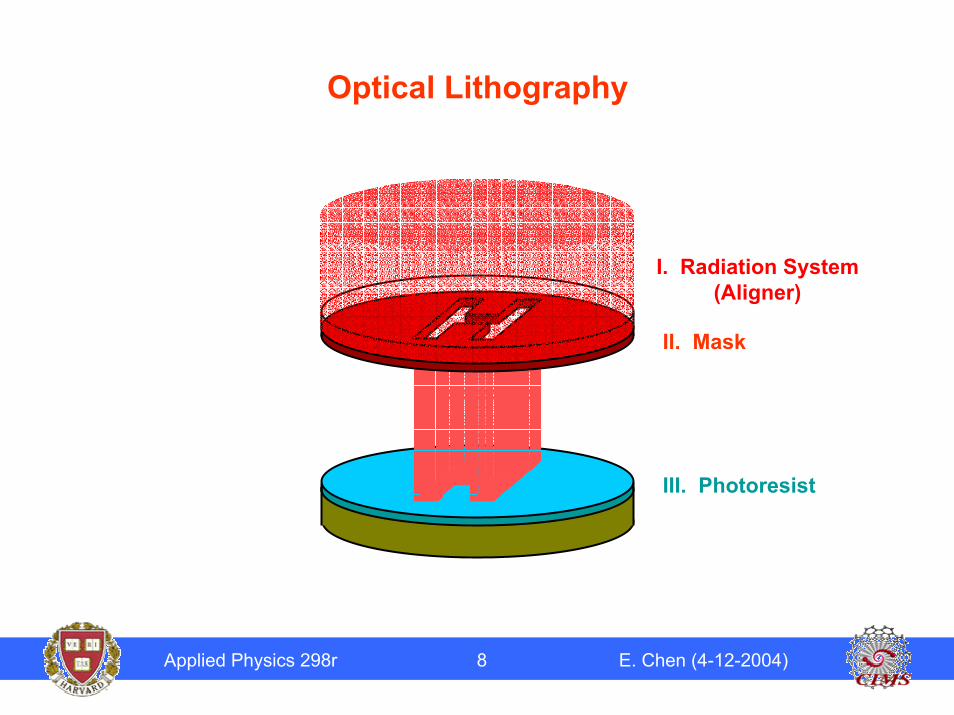
Optical Lithography
I. Radiation System(Aligner)
II. Mask
III. Photoresist
Applied Physics 298r 9 E. Chen (4-12-2004)
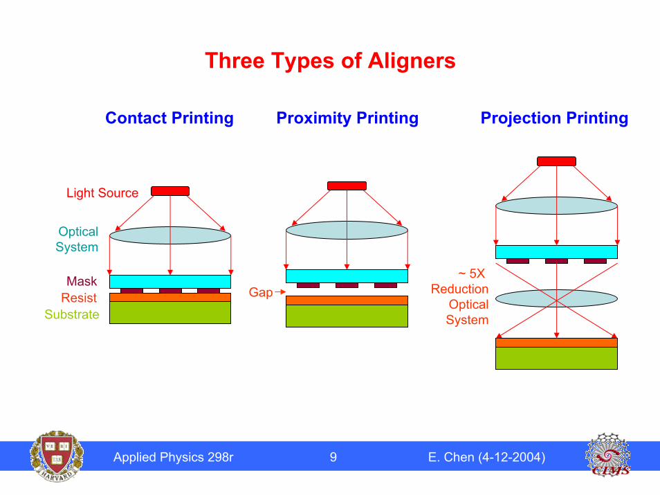
Three Types of Aligners
Contact Printing Proximity Printing Projection Printing
~ 5X Reduction
OpticalSystem
Gap
Light Source
OpticalSystem
MaskResist
Substrate
Applied Physics 298r 10 E. Chen (4-12-2004)
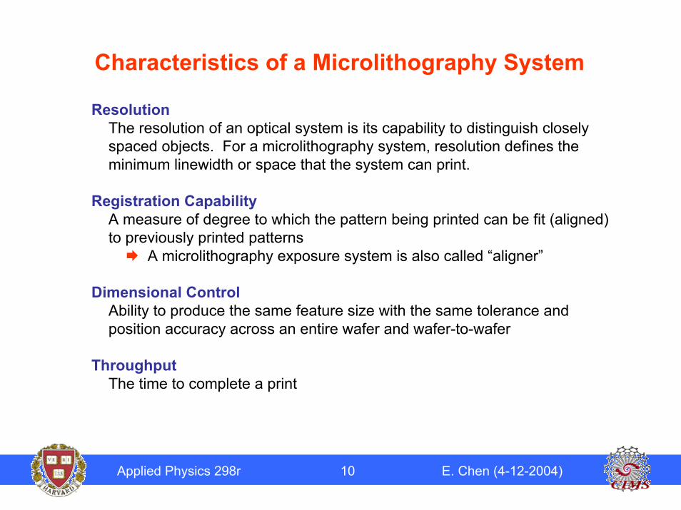
Characteristics of a Microlithography System
ResolutionThe resolution of an optical system is its capability to distinguish closely spaced objects. For a microlithography system, resolution defines the minimum linewidth or space that the system can print.
Registration CapabilityA measure of degree to which the pattern being printed can be fit (aligned) to previously printed patterns
A microlithography exposure system is also called “aligner”
Dimensional ControlAbility to produce the same feature size with the same tolerance and position accuracy across an entire wafer and wafer-to-wafer
ThroughputThe time to complete a print
Applied Physics 298r 11 E. Chen (4-12-2004)
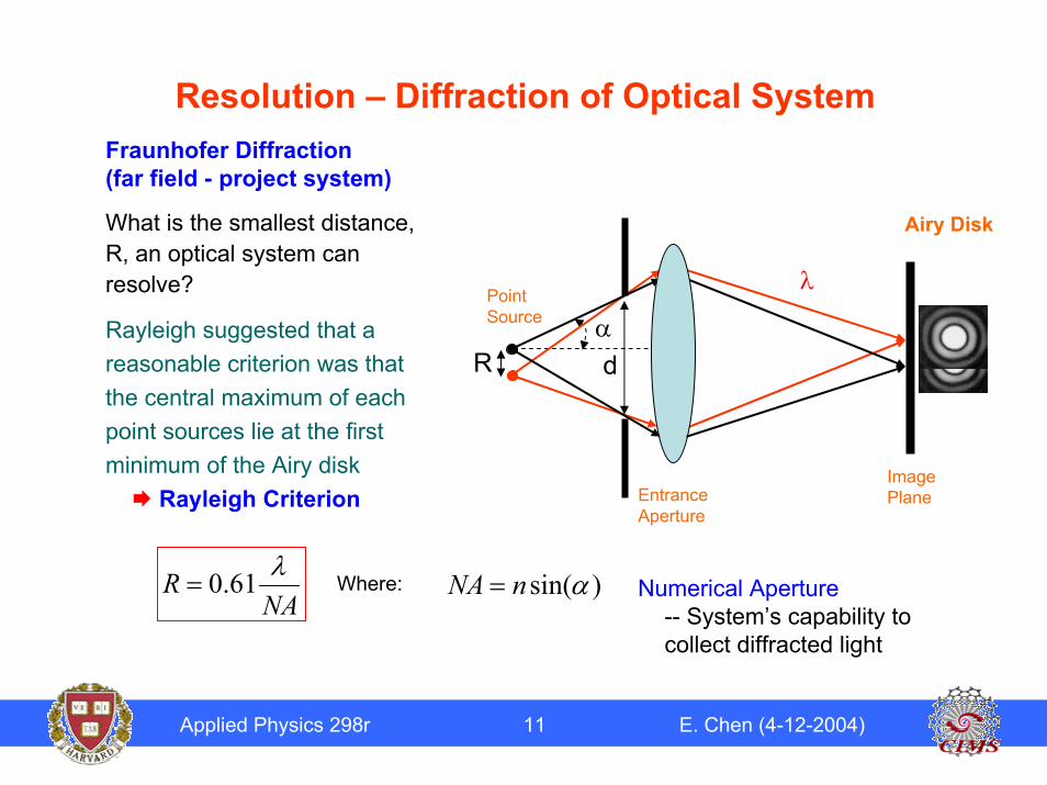
Resolution – Diffraction of Optical SystemFraunhofer Diffraction(far field - project system)
αdR
EntranceAperture
ImagePlane
PointSource
λ
Airy DiskWhat is the smallest distance, R, an optical system can resolve?
Rayleigh suggested that a reasonable criterion was that the central maximum of each point sources lie at the first minimum of the Airy disk
Rayleigh Criterion
NAR λ61.0= )sin(αnNA =Where: Numerical Aperture
-- System’s capability to collect diffracted light
Applied Physics 298r 12 E. Chen (4-12-2004)
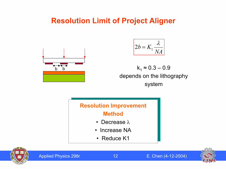
Resolution Limit of Project Aligner
NAKb λ12 =
b b k1 ≈ 0.3 – 0.9depends on the lithography
system
Resolution Improvement Method
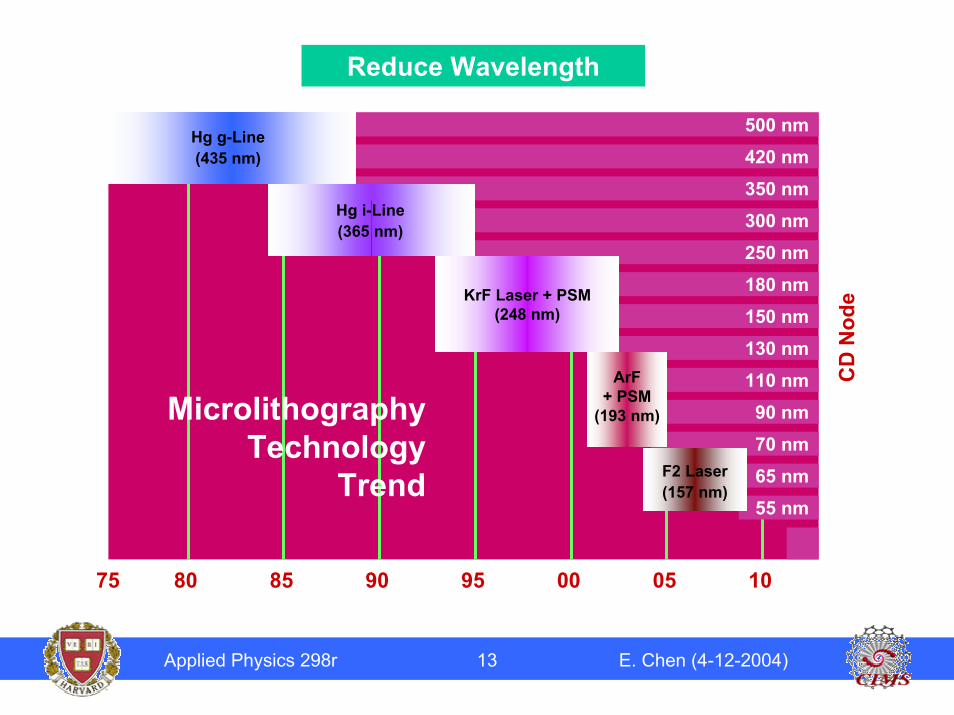
• Decrease λ• Increase NA• Reduce K1
Applied Physics 298r 13 E. Chen (4-12-2004)
Reduce Wavelength
MicrolithographyTechnology
Trend70 nm65 nm
250 nm180 nm150 nm130 nm110 nm90 nm
300 nm350 nm420 nm
80 85 90 95 00 05 10
55 nm
500 nm
75
Hg g-Line (435 nm)
Hg i-Line (365 nm)
KrF Laser + PSM (248 nm)
ArF+ PSM
(193 nm)
F2 Laser(157 nm)
CD
Nod
e
Applied Physics 298r 14 E. Chen (4-12-2004)
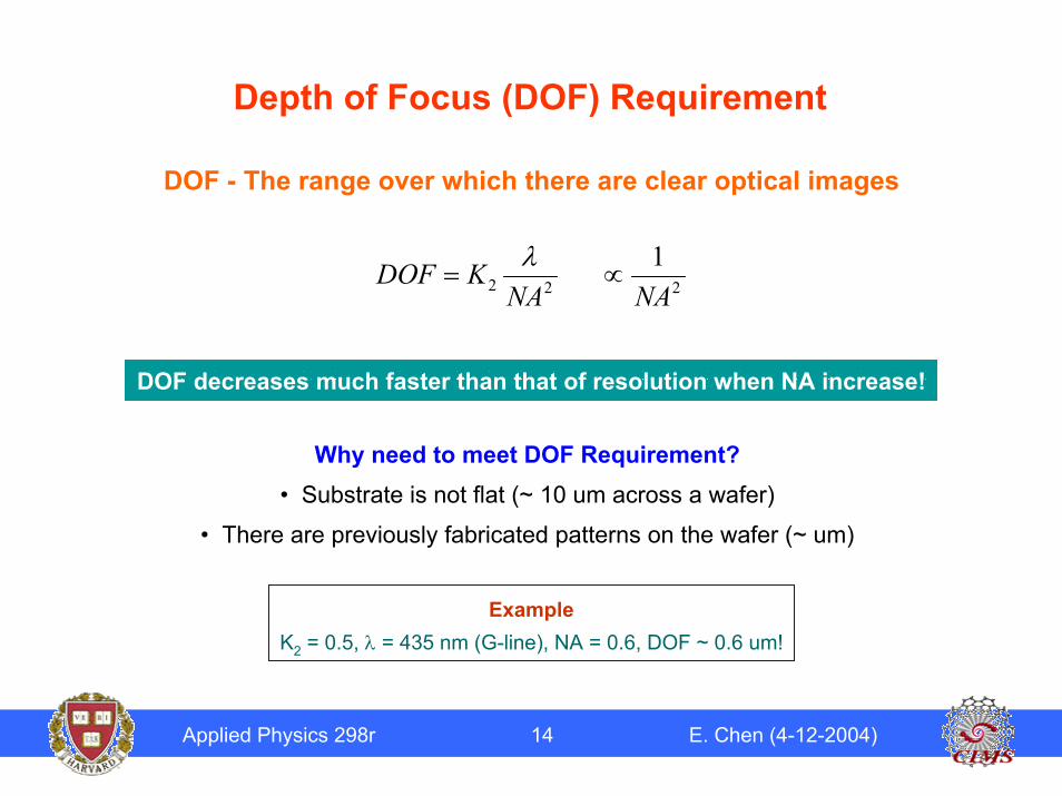
Depth of Focus (DOF) Requirement
DOF - The range over which there are clear optical images
2221NANA
KDOF ∝=λ
DOF decreases much faster than that of resolution when NA increase!
Why need to meet DOF Requirement?• Substrate is not flat (~ 10 um across a wafer)
• There are previously fabricated patterns on the wafer (~ um)
ExampleK2 = 0.5, λ = 435 nm (G-line), NA = 0.6, DOF ~ 0.6 um!
Applied Physics 298r 15 E. Chen (4-12-2004)
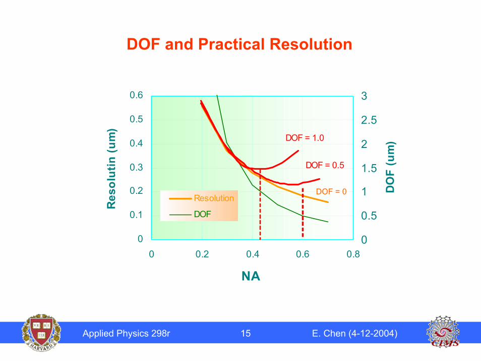
DOF and Practical Resolution
0
0.1
0.2
0.3
0.4
0.5
0.6
0 0.2 0.4 0.6 0.8
NA
Res
olut
in (u
m)
0
0.5
1
1.5
2
2.5
3
DO
F (u
m)
Resolution
DOF
DOF = 1.0
DOF = 0.5
DOF = 0
Applied Physics 298r 16 E. Chen (4-12-2004)
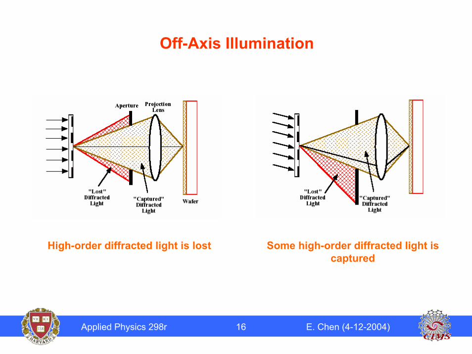
Off-Axis Illumination
High-order diffracted light is lost Some high-order diffracted light is captured
Applied Physics 298r 17 E. Chen (4-12-2004)
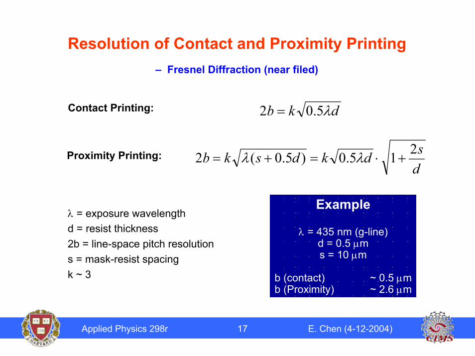
Resolution of Contact and Proximity Printing– Fresnel Diffraction (near filed)
Contact Printing: dkb λ5.02 =
dsdkdskb 215.0)5.0(2 +⋅=+= λλProximity Printing:
Example
λ = 435 nm (g-line)d = 0.5 µms = 10 µm
b (contact) ~ 0.5 µmb (Proximity) ~ 2.6 µm
λ = exposure wavelengthd = resist thickness2b = line-space pitch resolutions = mask-resist spacingk ~ 3
Applied Physics 298r 18 E. Chen (4-12-2004)
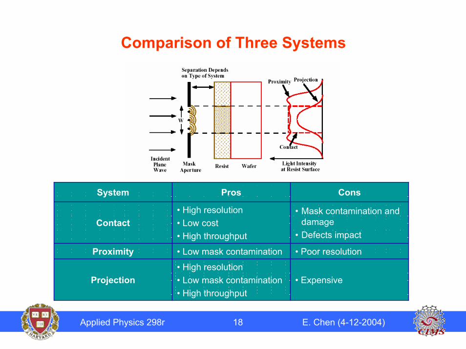
Comparison of Three Systems
• Expensive• High resolution• Low mask contamination• High throughput
Projection
• Poor resolution• Low mask contaminationProximity
• Mask contamination and damage
• Defects impact
• High resolution• Low cost• High throughput
Contact
ConsProsSystem
Applied Physics 298r 19 E. Chen (4-12-2004)
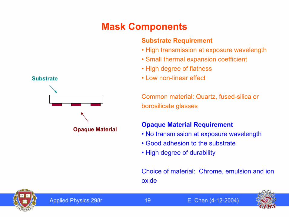
Mask ComponentsSubstrate Requirement• High transmission at exposure wavelength• Small thermal expansion coefficient• High degree of flatness• Low non-linear effect
Common material: Quartz, fused-silica or borosilicate glasses
Opaque Material Requirement• No transmission at exposure wavelength• Good adhesion to the substrate• High degree of durability
Choice of material: Chrome, emulsion and ion oxide
Substrate
Opaque Material
Applied Physics 298r 20 E. Chen (4-12-2004)
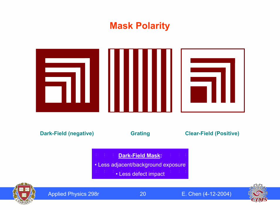
Mask Polarity
Dark-Field (negative) Grating Clear-Field (Positive)
Dark-Field Mask:• Less adjacent/background exposure
• Less defect impact
Applied Physics 298r 21 E. Chen (4-12-2004)
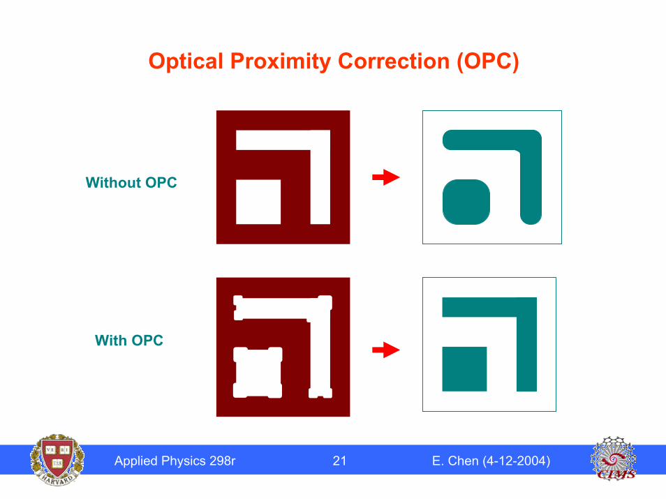
Optical Proximity Correction (OPC)
Without OPC
With OPC
Applied Physics 298r 22 E. Chen (4-12-2004)
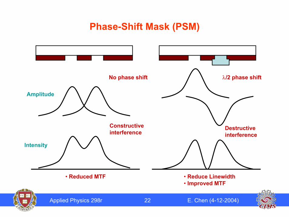
Phase-Shift Mask (PSM)
λ/2 phase shift
• Reduce Linewidth• Improved MTF
Destructiveinterference
No phase shift
Constructiveinterference
Intensity
Amplitude
• Reduced MTF
Applied Physics 298r 23 E. Chen (4-12-2004)
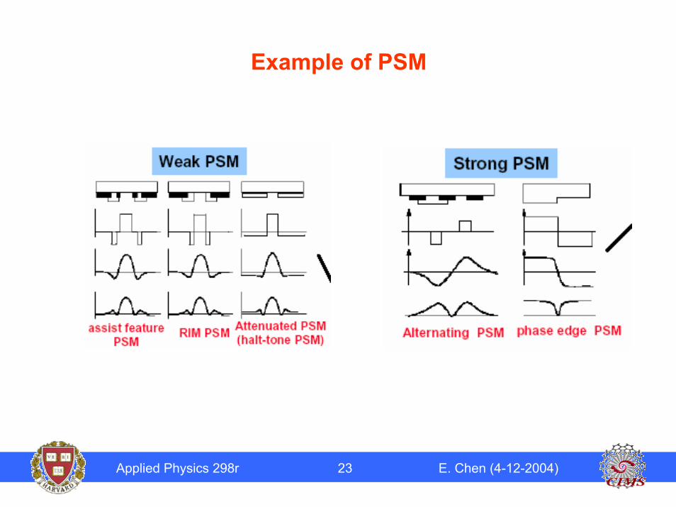
Example of PSM
Applied Physics 298r 24 E. Chen (4-12-2004)
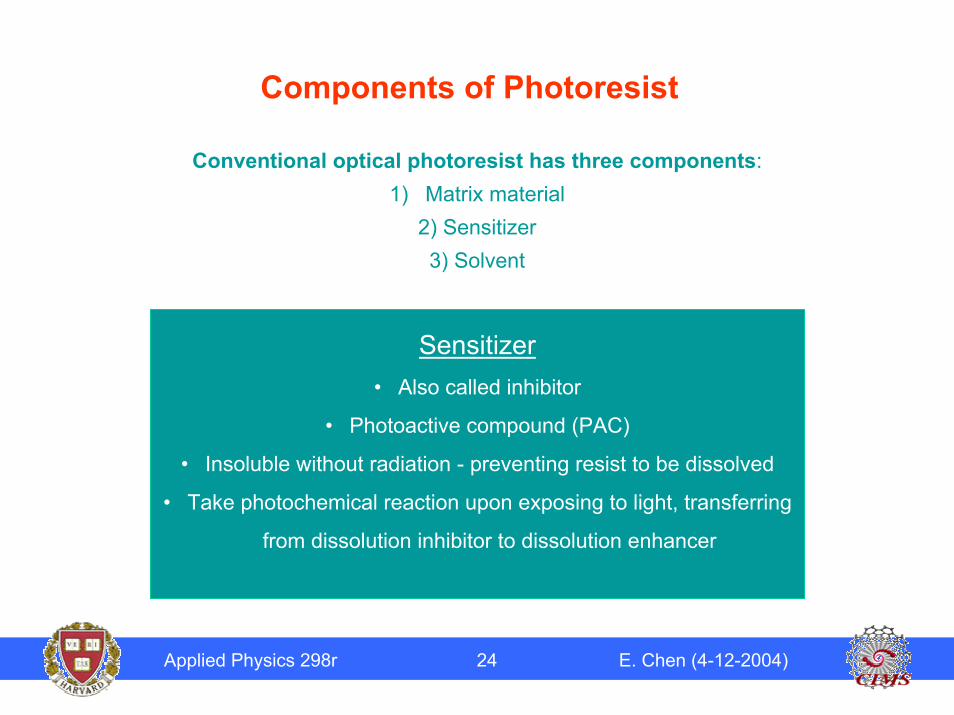
Components of Photoresist
Conventional optical photoresist has three components:1) Matrix material
2) Sensitizer3) Solvent
Sensitizer• Also called inhibitor
• Photoactive compound (PAC)
• Insoluble without radiation - preventing resist to be dissolved
• Take photochemical reaction upon exposing to light, transferring
from dissolution inhibitor to dissolution enhancer
Applied Physics 298r 25 E. Chen (4-12-2004)
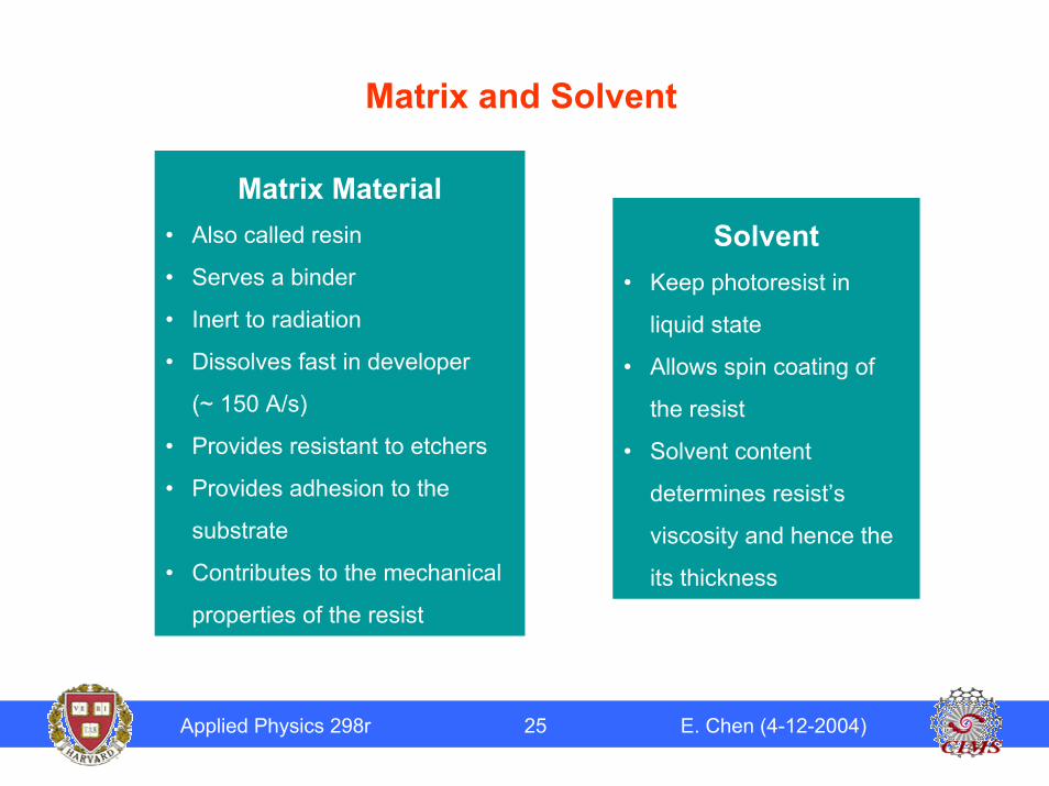
Matrix and Solvent
Matrix Material• Also called resin
• Serves a binder
• Inert to radiation
• Dissolves fast in developer
(~ 150 A/s)
• Provides resistant to etchers
• Provides adhesion to the
substrate
• Contributes to the mechanical
properties of the resist
Solvent• Keep photoresist in
liquid state
• Allows spin coating of
the resist
• Solvent content
determines resist’s
viscosity and hence the
its thickness
Applied Physics 298r 26 E. Chen (4-12-2004)
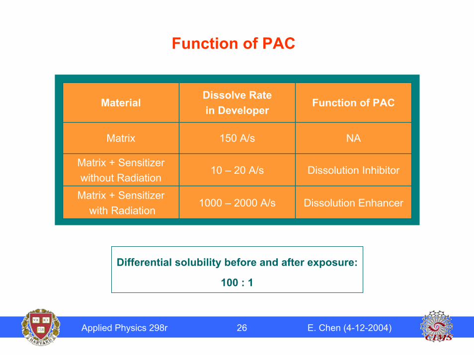
Function of PAC
Dissolution Enhancer1000 – 2000 A/sMatrix + Sensitizer
with Radiation
Dissolution Inhibitor10 – 20 A/sMatrix + Sensitizerwithout Radiation
NA150 A/sMatrix
Function of PACDissolve Ratein Developer
Material
Differential solubility before and after exposure:
100 : 1
Applied Physics 298r 27 E. Chen (4-12-2004)
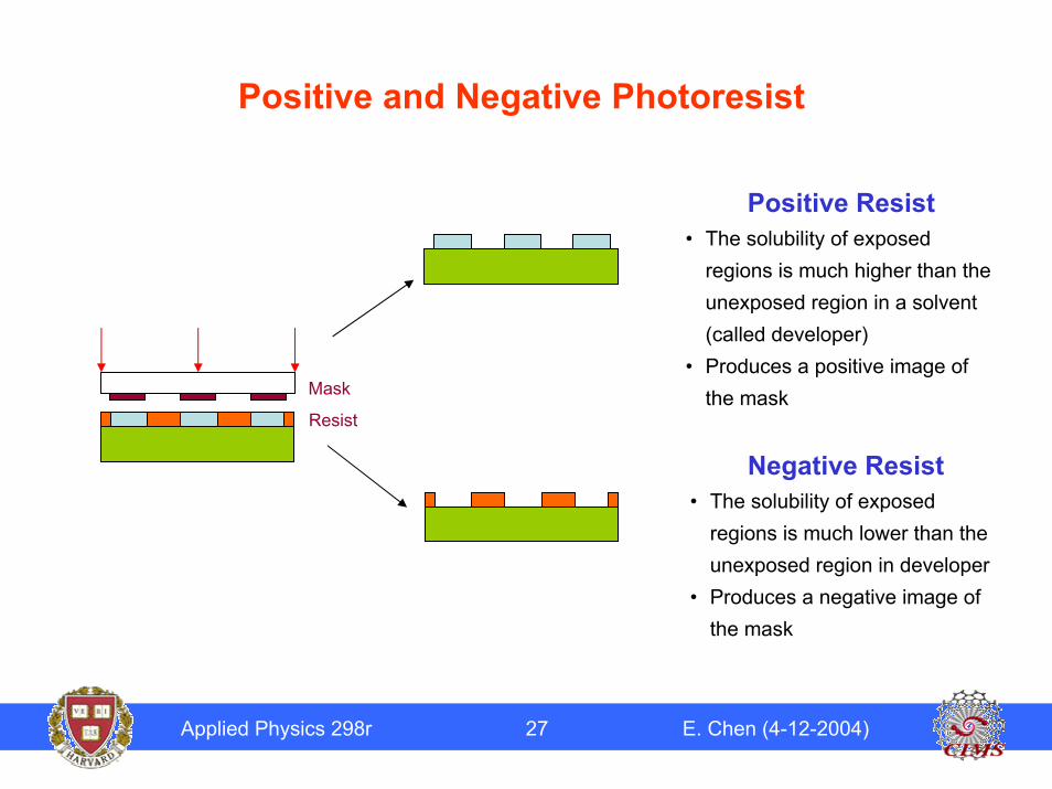
Positive and Negative Photoresist
Positive Resist• The solubility of exposed
regions is much higher than the unexposed region in a solvent (called developer)
• Produces a positive image of the mask
Negative Resist• The solubility of exposed
regions is much lower than the unexposed region in developer
• Produces a negative image of the mask
Mask
Resist
Applied Physics 298r 28 E. Chen (4-12-2004)
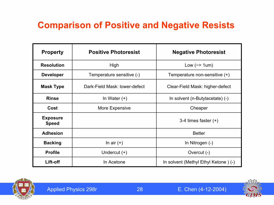
Comparison of Positive and Negative Resists
Lift-off
Profile
Backing
Adhesion
Exposure Speed
Cost
Rinse
Mask Type
Developer
Resolution
Property
3-4 times faster (+)
CheaperMore Expensive
Better
In Nitrogen (-)In air (+)
Overcut (-)Undercut (+)
In solvent (Methyl Ethyl Ketone ) (-)In Acetone
In solvent (n-Butylacetate) (-)In Water (+)
Temperature non-sensitive (+)Temperature sensitive (-)
Clear-Field Mask: higher-defectDark-Field Mask: lower-defect
Low (~> 1um)High
Negative PhotoresistPositive Photoresist
Applied Physics 298r 29 E. Chen (4-12-2004)
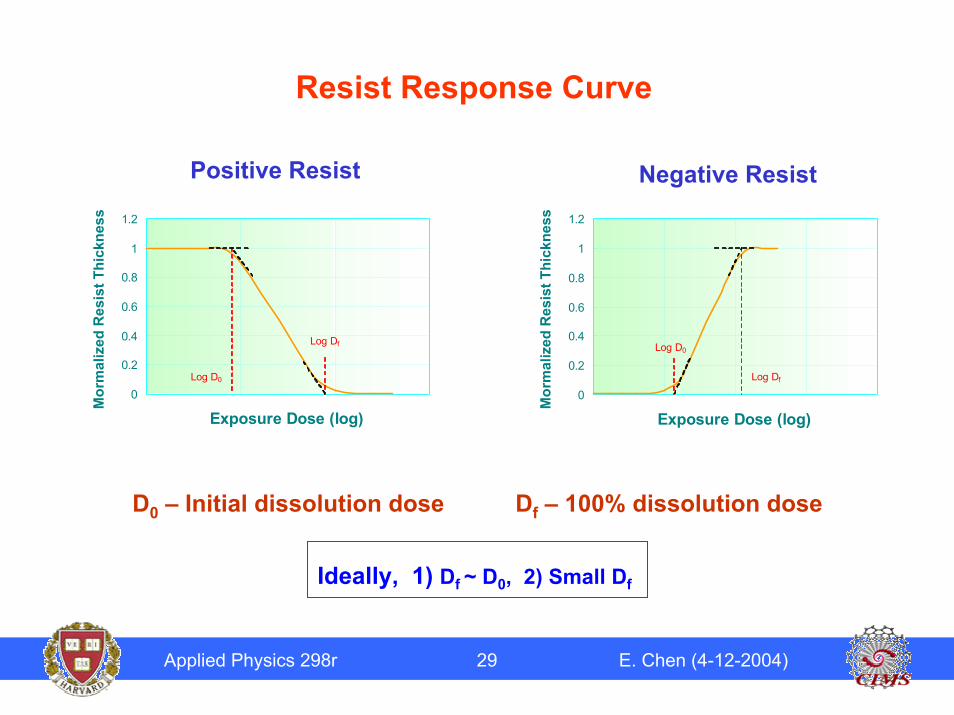
Resist Response Curve
0
0.2
0.4
0.6
1
1.2
Exposure Dose (log)
Mor
mal
ized
Res
ist T
hick
ness
Log D0
Log Df
Positive Resist
0
0.2
0.4
0.6
0.8
1
1.2
Exposure Dose (log)
Mor
mal
ized
Res
ist T
hick
ness
Log D0
Log Df
Negative Resist
0.8
D0 – Initial dissolution dose Df – 100% dissolution dose
Ideally, 1) Df ~ D0, 2) Small Df
Applied Physics 298r 30 E. Chen (4-12-2004)
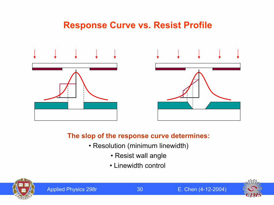
Response Curve vs. Resist Profile
The slop of the response curve determines:• Resolution (minimum linewidth)
• Resist wall angle• Linewidth control
Applied Physics 298r 31 E. Chen (4-12-2004)
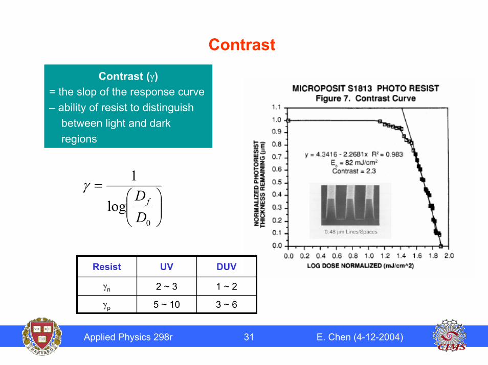
Contrast
=
0
log
1
DDf
γ
Contrast (γ)= the slop of the response curve– ability of resist to distinguish
between light and dark regions
3 ~ 65 ~ 10γp
1 ~ 22 ~ 3γn
DUV UVResist
Applied Physics 298r 32 E. Chen (4-12-2004)
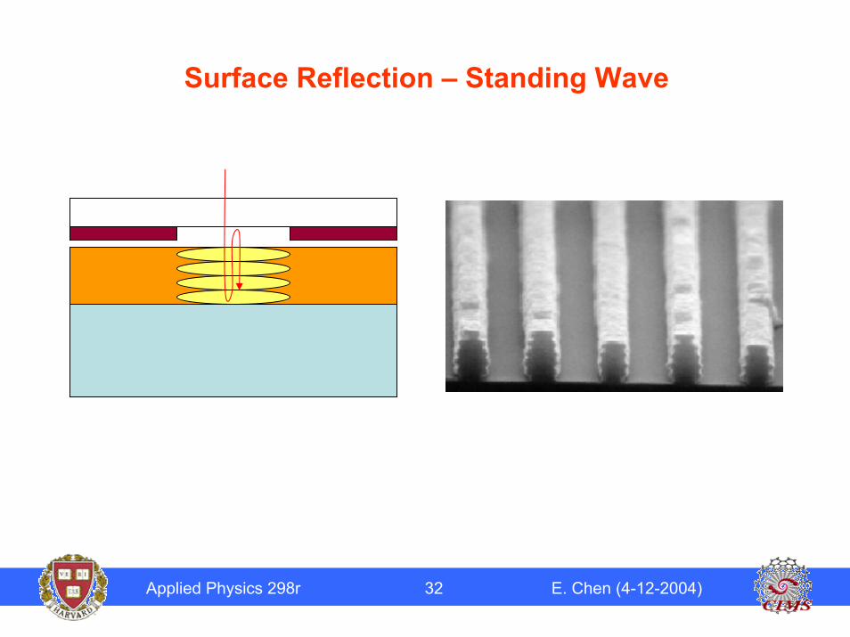
Surface Reflection – Standing Wave
Applied Physics 298r 33 E. Chen (4-12-2004)
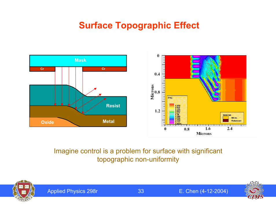
Surface Topographic Effect
Resist
Mask
CrCr
Oxide Metal
Imagine control is a problem for surface with significant topographic non-uniformity
Applied Physics 298r 34 E. Chen (4-12-2004)
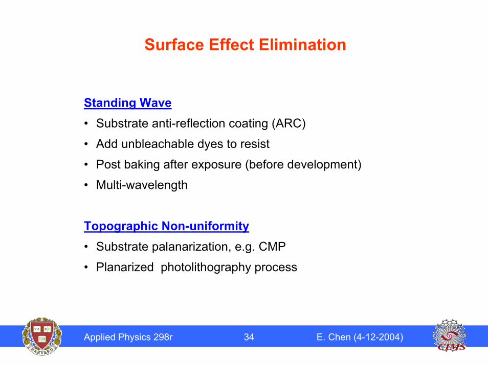
Surface Effect Elimination
Standing Wave• Substrate anti-reflection coating (ARC)
• Add unbleachable dyes to resist
• Post baking after exposure (before development)
• Multi-wavelength
Topographic Non-uniformity• Substrate palanarization, e.g. CMP
• Planarized photolithography process
Applied Physics 298r 35 E. Chen (4-12-2004)
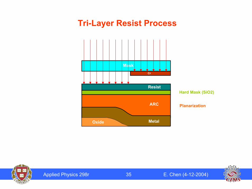
Tri-Layer Resist Process
Mask
Cr
ARC
ResistHard Mask (SiO2)
Planarization
Oxide Metal
Applied Physics 298r 36 E. Chen (4-12-2004)
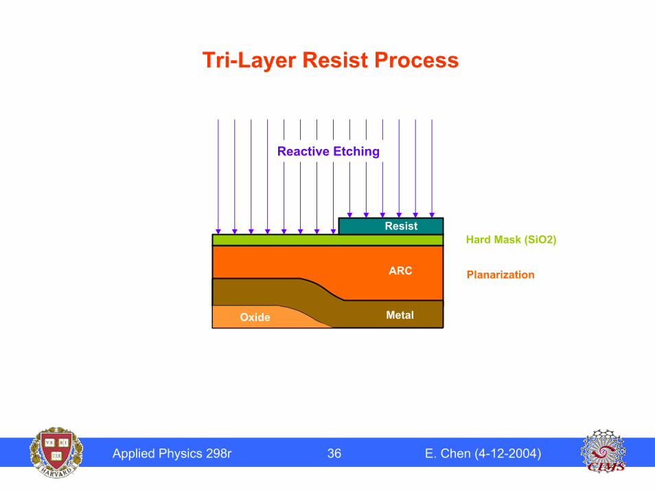
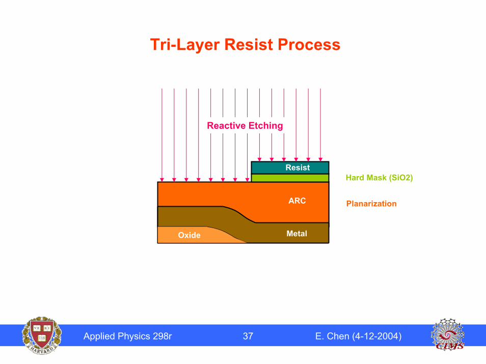
Tri-Layer Resist Process
ARC
Resist
Reactive Etching
Hard Mask (SiO2)
Planarization
Oxide Metal
Applied Physics 298r 37 E. Chen (4-12-2004)
Tri-Layer Resist Process
ARC
Resist
ARC
Reactive Etching
Hard Mask (SiO2)
Planarization
Oxide Metal
Applied Physics 298r 38 E. Chen (4-12-2004)
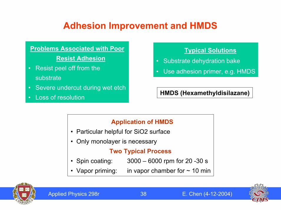
Adhesion Improvement and HMDS
Problems Associated with Poor Resist Adhesion
• Resist peel off from the substrate
• Severe undercut during wet etch• Loss of resolution
Typical Solutions• Substrate dehydration bake
• Use adhesion primer, e.g. HMDS
HMDS (Hexamethyldisilazane)
Application of HMDS• Particular helpful for SiO2 surface• Only monolayer is necessary
Two Typical Process• Spin coating: 3000 – 6000 rpm for 20 -30 s• Vapor priming: in vapor chamber for ~ 10 min
Applied Physics 298r 39 E. Chen (4-12-2004)
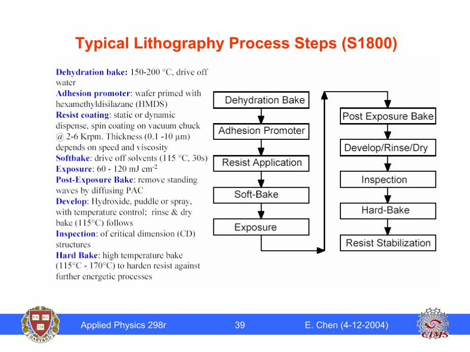
Typical Lithography Process Steps (S1800)
Applied Physics 298r 40 E. Chen (4-12-2004)
Advanced Lithography Technology
• E-Beam Lithography
• X-Ray Lithography
• Focused Ion Beam Lithography
• Alternative Lithography• Soft-lithography• Imprinting lithography
Applied Physics 298r 41 E. Chen (4-12-2004)
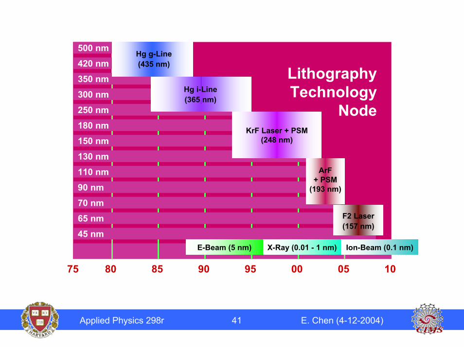
LithographyTechnology
Node
70 nm65 nm
250 nm180 nm150 nm130 nm110 nm90 nm
300 nm350 nm420 nm
45 nm
500 nmHg g-Line (435 nm)
Hg i-Line (365 nm)
KrF Laser + PSM (248 nm)
ArF+ PSM
(193 nm)
F2 Laser(157 nm)
E-Beam (5 nm) X-Ray (0.01 - 1 nm) Ion-Beam (0.1 nm)
75 80 85 90 95 00 05 10
Applied Physics 298r 42 E. Chen (4-12-2004)
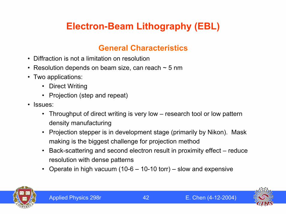
Electron-Beam Lithography (EBL)
General Characteristics• Diffraction is not a limitation on resolution• Resolution depends on beam size, can reach ~ 5 nm• Two applications:
• Direct Writing • Projection (step and repeat)
• Issues:• Throughput of direct writing is very low – research tool or low pattern
density manufacturing• Projection stepper is in development stage (primarily by Nikon). Mask
making is the biggest challenge for projection method• Back-scattering and second electron result in proximity effect – reduce
resolution with dense patterns• Operate in high vacuum (10-6 – 10-10 torr) – slow and expensive
Applied Physics 298r 43 E. Chen (4-12-2004)
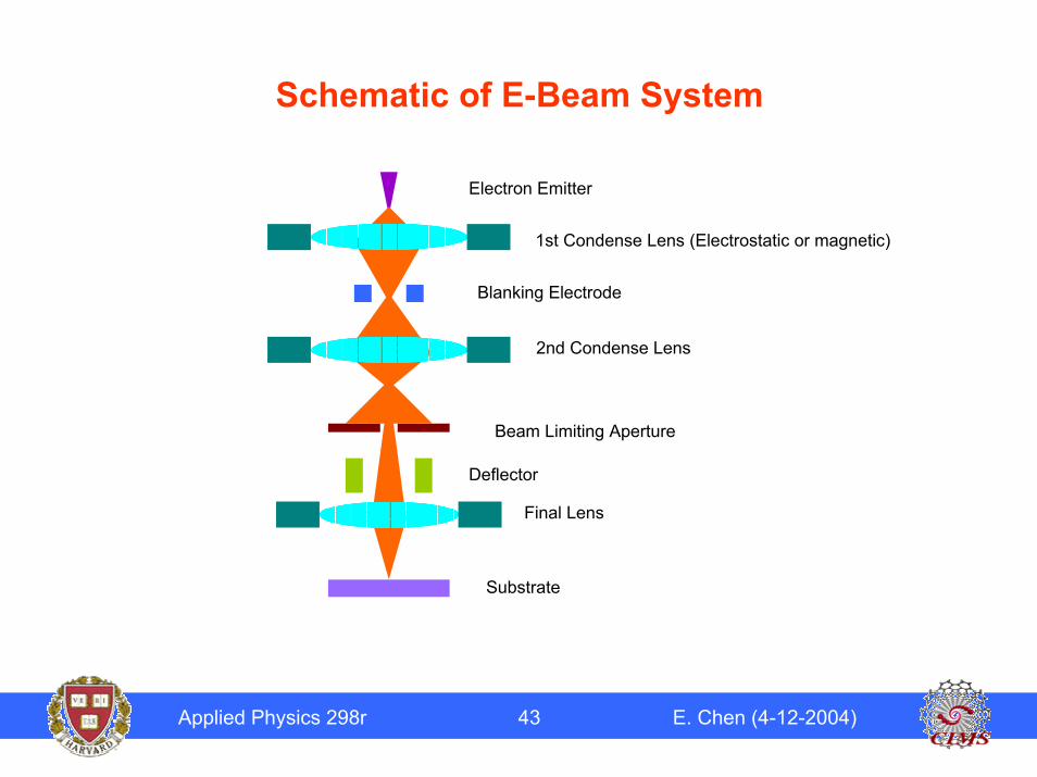
Schematic of E-Beam System
Electron Emitter
1st Condense Lens (Electrostatic or magnetic)
Blanking Electrode
2nd Condense Lens
Beam Limiting Aperture
Deflector
Final Lens
Substrate
Applied Physics 298r 44 E. Chen (4-12-2004)
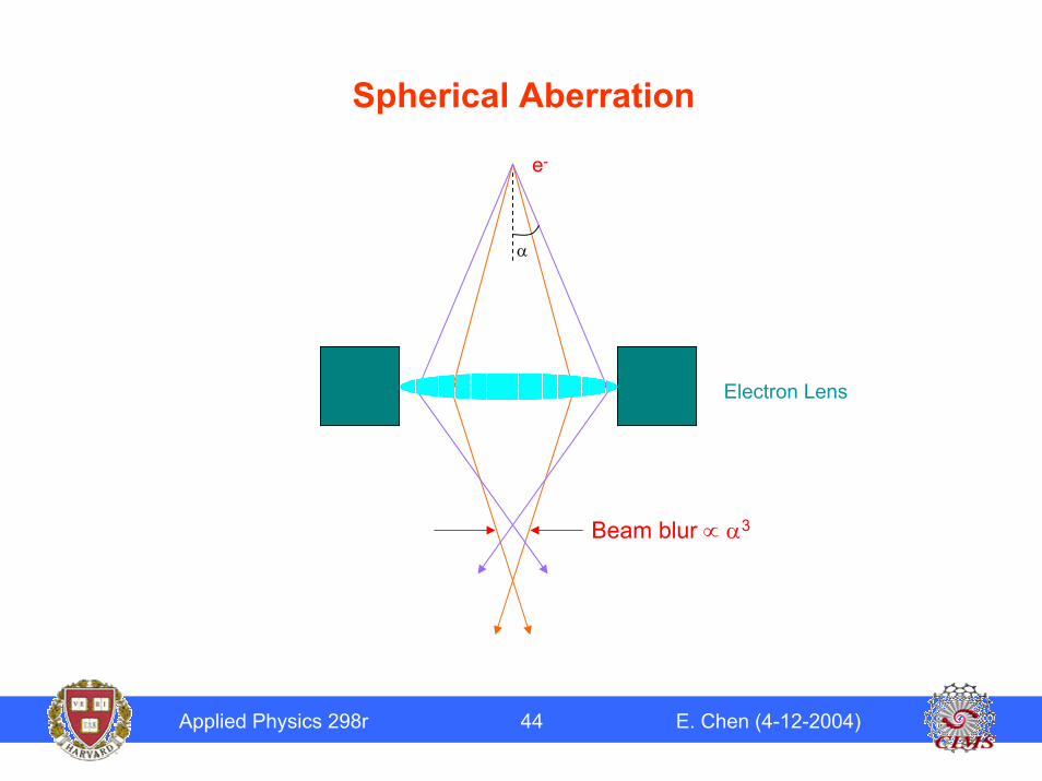
Spherical Aberration
Beam blur ∝ α3
e-
α
Electron Lens
Applied Physics 298r 45 E. Chen (4-12-2004)
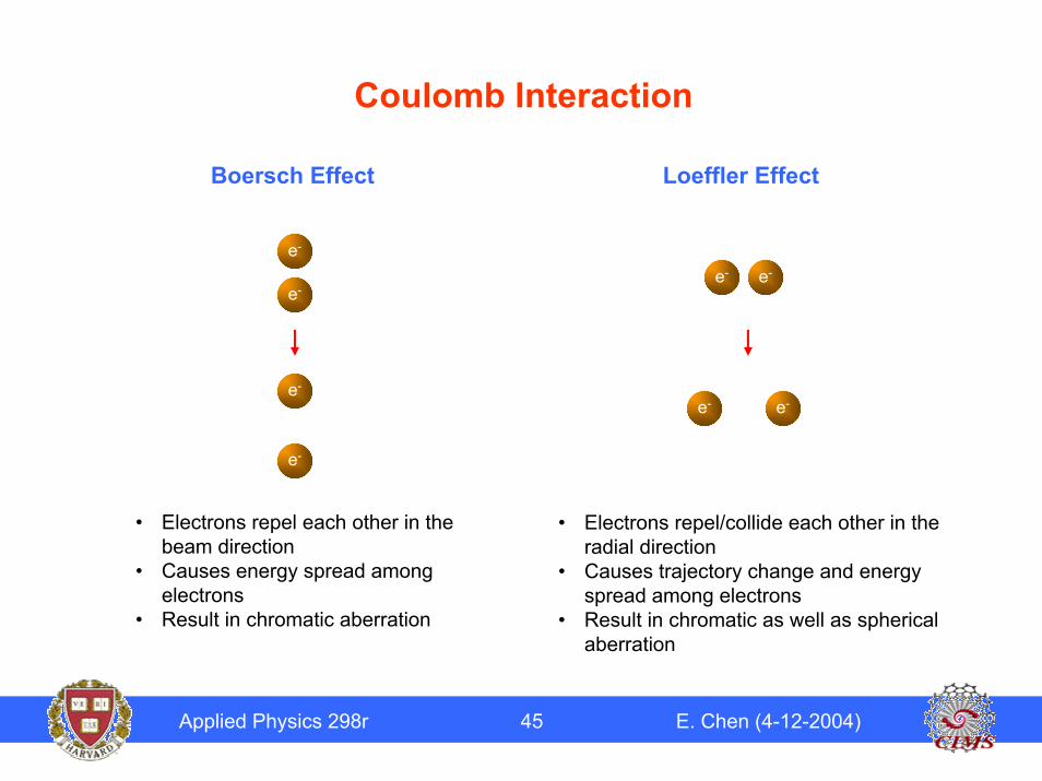
Coulomb Interaction
Boersch Effect Loeffler Effect
e-
e-e- e-
e-
e-
e- e-
• Electrons repel each other in the beam direction
• Causes energy spread among electrons
• Result in chromatic aberration
• Electrons repel/collide each other in the radial direction
• Causes trajectory change and energy spread among electrons
• Result in chromatic as well as spherical aberration
Applied Physics 298r 46 E. Chen (4-12-2004)
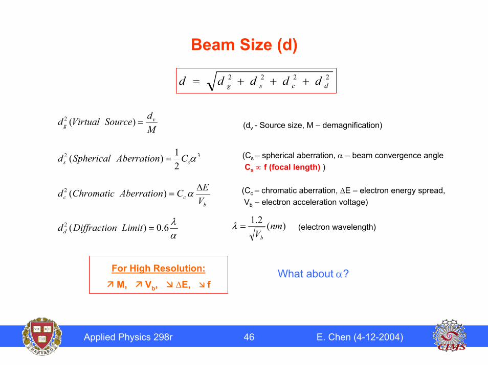
Beam Size (d)
2222dcsg ddddd +++=
MdSourceVirtuald v
g =)(2 (dv - Source size, M – demagnification)
32
21)( αss CAberrationSphericald = (Cs – spherical aberration, α – beam convergence angle
Cs ∝ f (focal length) )
bcc V
ECAberrationChromaticd ∆= α)(2 (Cc – chromatic aberration, ∆E – electron energy spread,
Vb – electron acceleration voltage)
)(2.1 nmVb
=λαλ6.0)(2 =LimitnDiffractiodd (electron wavelength)
For High Resolution:M, Vb, ∆E, f
What about α?
Applied Physics 298r 47 E. Chen (4-12-2004)
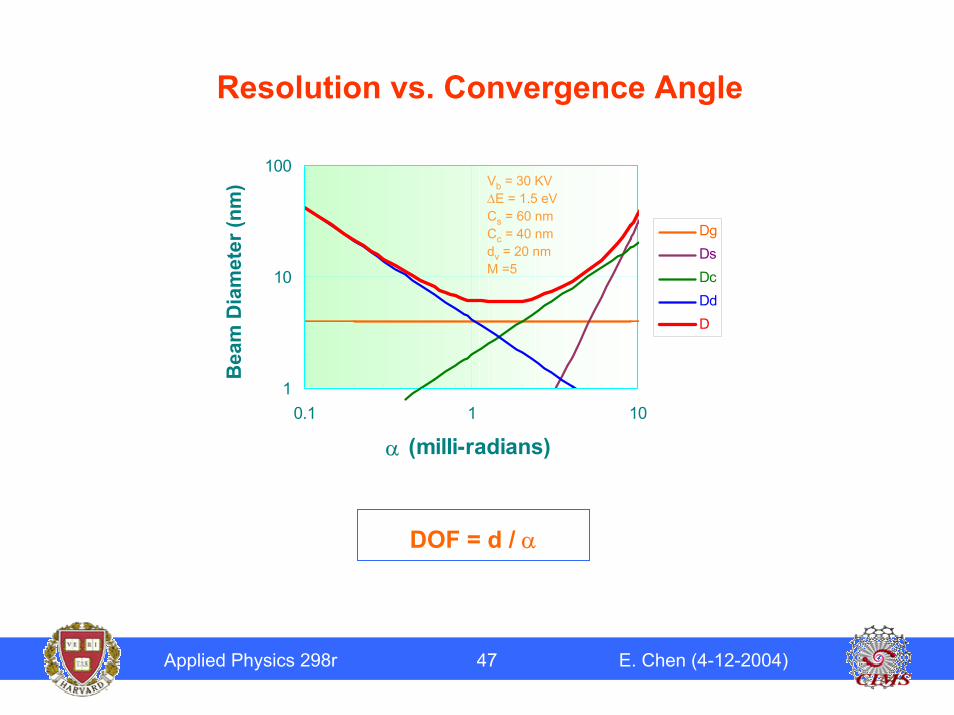
1
10
100
0.1 1 10
α (milli-radians)
Bea
m D
iam
eter
(nm
)DgDsDcDdD
Resolution vs. Convergence Angle
Vb = 30 KV∆E = 1.5 eVCs = 60 nmCc = 40 nmdv = 20 nmM =5
DOF = d / α
Applied Physics 298r 48 E. Chen (4-12-2004)
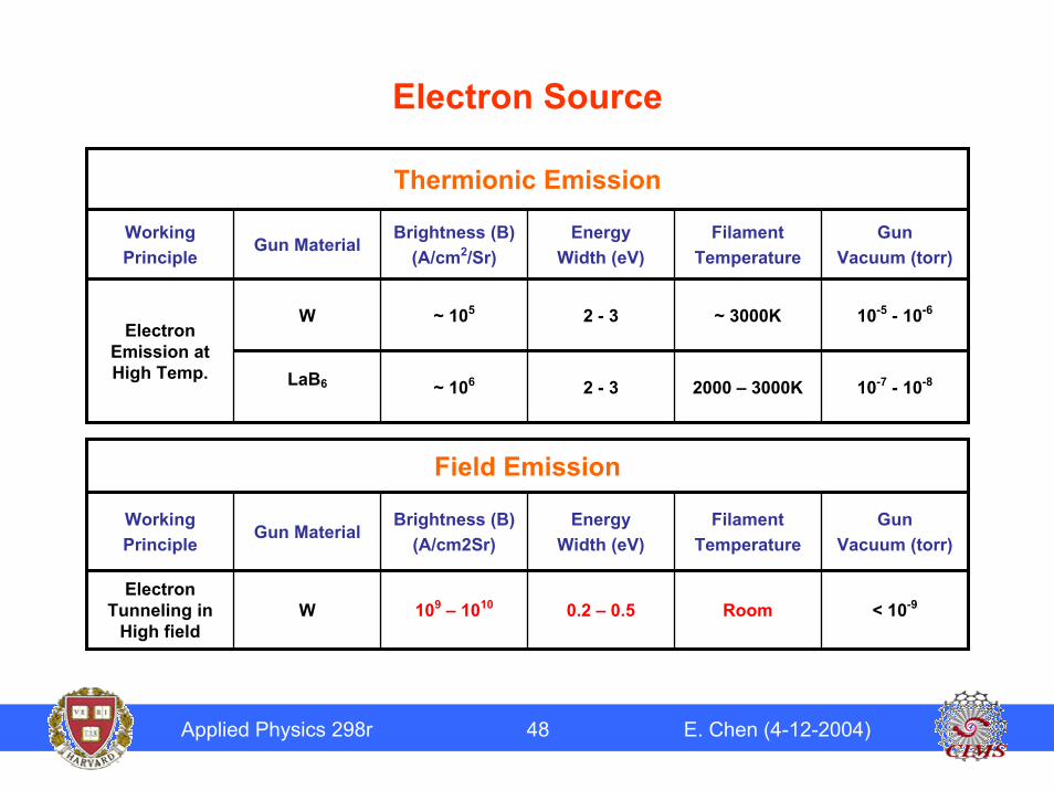
Electron Source
Field Emission
< 10-9
GunVacuum (torr)
FilamentTemperature
EnergyWidth (eV)
Brightness (B)(A/cm2Sr)
Gun MaterialWorkingPrinciple
Room0.2 – 0.5109 – 1010WElectron
Tunneling in High field
10-7 - 10-82000 – 3000K2 - 3~ 106LaB6
Thermionic Emission
10-5 - 10-6
GunVacuum (torr)
FilamentTemperature
EnergyWidth (eV)
Brightness (B)(A/cm2/Sr)
Gun MaterialWorkingPrinciple
~ 3000K2 - 3~ 105WElectron
Emission at High Temp.
Applied Physics 298r 49 E. Chen (4-12-2004)
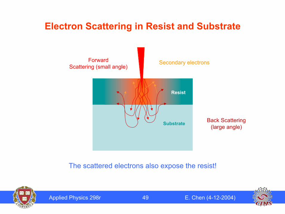
Electron Scattering in Resist and Substrate
e-
Resist
Substrate
ForwardScattering (small angle)
Secondary electrons
Back Scattering(large angle)
The scattered electrons also expose the resist!
Applied Physics 298r 50 E. Chen (4-12-2004)
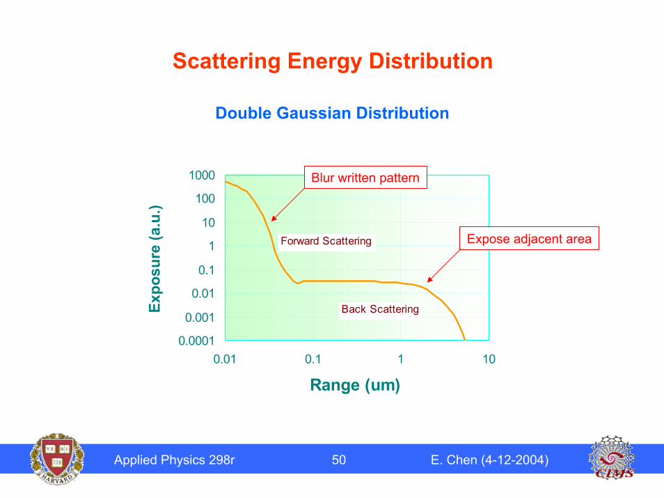
Scattering Energy Distribution
0.0001
0.001
0.01
0.1
1
10
100
1000
0.01 0.1 1 10
Range (um)
Expo
sure
(a.u
.)
Forward Scattering
Back Scattering
Double Gaussian Distribution
Blur written pattern
Expose adjacent area
Applied Physics 298r 51 E. Chen (4-12-2004)
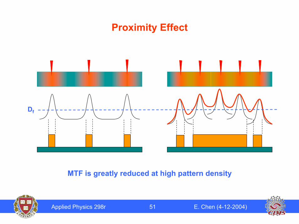
Proximity Effect
Df
MTF is greatly reduced at high pattern density
Applied Physics 298r 52 E. Chen (4-12-2004)
Proximity Effect Correction
• Use thin resist
• Use thin substrate
• Adjust acceleration voltage
• Split pattern into several writings using different
doses
• Adjust pattern size and shapes (remember diffraction
correction in mask engineering?)
• Adjust dose level to compensate scattering
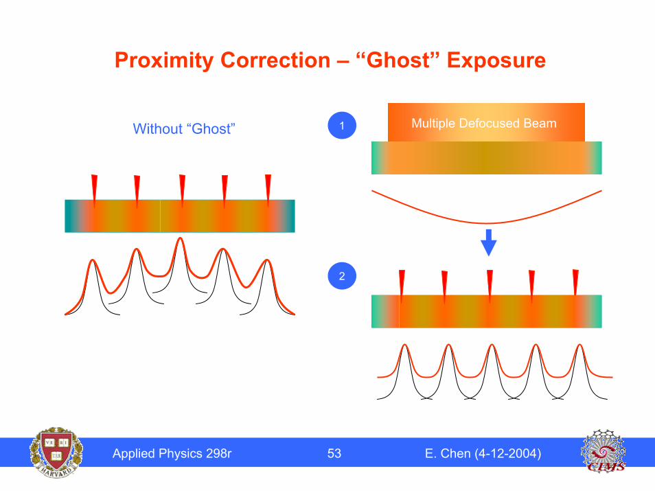
Applied Physics 298r 53 E. Chen (4-12-2004)
Proximity Correction – “Ghost” Exposure
1 Multiple Defocused BeamWithout “Ghost”
2
Applied Physics 298r 54 E. Chen (4-12-2004)
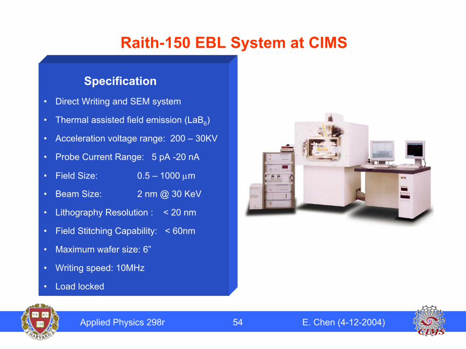
Raith-150 EBL System at CIMS
Specification• Direct Writing and SEM system
• Thermal assisted field emission (LaB6)
• Acceleration voltage range: 200 – 30KV
• Probe Current Range: 5 pA -20 nA
• Field Size: 0.5 – 1000 µm
• Beam Size: 2 nm @ 30 KeV
• Lithography Resolution : < 20 nm
• Field Stitching Capability: < 60nm
• Maximum wafer size: 6”
• Writing speed: 10MHz
• Load locked