Embed Size (px)
Citation preview

M AN819Implementing Bootloader Firmware for the PIC18C601/801 ROMless Microcontrollers
INTRODUCTION
The PIC18C601 and PIC18C801 microcontrollers arethe first members of Microchip’s PIC18 family with noon-chip program memory. They offer the PIC18 archi-tecture, with the ability to use different types and sizesof external program memory (up to 2 Mbyte) to exactlyfit most applications.
In modern embedded applications, where features andfunctionality are constantly evolving, FLASH memory isan ideal choice for external program memory. Fieldupgradability is almost always desirable in these sys-tems, too. Most commonly available FLASH devices,however, disable read access while being programmedor erased. They also require special commandsequences for programming, and have longer eraseand write times than read times. As a result, systemsusing FLASH technology require either a second mem-ory device, or a microcontroller with built-in memoryspace, in order to implement field reprogrammability.PIC18C601/801 controllers do this by allowing part ofon-chip data memory to be reconfigured as programmemory.
To implement reprogrammability, the user must incor-porate into their design, a bootloader — a firmwaremechanism that allows a new user application programto be written to the system. The bootloader firmwaresystem must be able to recognize that new user codeis available and initiate itself (“invocation”), receive thenew code from some communication channel in man-ageable segments and check it for communicationerrors (“communication”), and program the memorywith the new data and without errors (“programming”).It must also be flexible enough to be able to incorporatenew programming methods, as new FLASH devicesbecome available.
This application note discusses the general designrequirements for bootloader firmware in a ROMlesscontroller system. To illustrate the key points, a fully-featured reference design, with an interface to externalhost software, is described in detail. Information onintegrating a bootloader with user application code isalso covered.
The reader is expected to be familiar with the following:
• General PIC18 architecture
• The PIC18 instruction set• External memory interface modes of the PIC18
ROMless devices, and• Interface modes of different non-volatile memory
devices
PROGRAMMING A ROMLESS SYSTEM: OVERVIEW
PIC18C601/801 controllers offer no on-chip programmemory. In normal operation, program instructions arefetched and executed directly from the external mem-ory. These microcontrollers also offer 1.5 Kbytes of on-chip data memory. Of this, the last 512 bytes are des-ignated as “Boot RAM”. This block can be configured toact as either data or program memory; when set as pro-gram memory, it provides the system designer a way toprogram external FLASH devices without the need foradditional hardware. The memory maps for the control-lers, showing Boot RAM enabled and disabled, arepresented in Figures 1 and 2.
When programs are executed from Boot RAM, the sys-tem bus and all of its control signals are deactivated. Ifrequired, the external system bus may be disabled andturned into I/O port signals. While the Boot RAM isenabled, any attempts to read or write to it are ignored.Any TBLWT instructions attempted to addresses in theBoot RAM space result in an external table write to theexternal memory, instead. Similarly, TBLRD instructionson the Boot RAM space, are performed on the externalmemory.
Authors: Gaurang Kavaiya andNilesh RajbhartiMicrochip Technology Inc.
2001 Microchip Technology Inc. DS00819A-page 1

AN819
A typical bootloader using the Boot RAM performs thefollowing steps:
1. Disable Boot RAM.2. Transfer the programmer routine of the boot-
loader program from the external program mem-ory to the Boot RAM, using TBLRD and MOVWFinstructions.
3. Enable the Boot RAM.
4. Execute the programmer routine as a data blockis received.
5. Perform the necessary programming on theexternal memory by either executing the neces-sary TBLRD and TBLWT instructions, or byswitching the system bus to I/O ports.
6. Continue to execute the programmer routinefrom Boot RAM as data blocks are received.
7. Jump to a known valid external program mem-ory location.
8. Reset the system when all data is programmed.
DS00819A-page 2 2001 Microchip Technology Inc.

AN819
FIGURE 1: MEMORY MAP AND PROGRAM STACK FOR THE PIC18C801
RESET Vector 0000h
High Priority Interrupt Vector 0008h
Low Priority Interrupt Vector 0018h
1FFFFFh
RESET Vector 0000h
High Priority Interrupt Vector 0008h
Low Priority Interrupt Vector 0018h
1FFFFFh
Use
r M
emor
y S
pace
PC<20:0>
Stack Level 1
Stack Level 31
1FFFFFh
Use
r M
emor
y S
pace
ExternalTable Memory
On-ChipBoot RAM
ExternalProgramMemory
Internal Memory External Memory
PGRM = ‘1’
PGRM = ‘0’
1FFE00h1FFDFFh
1FFE00h
ExternalProgramMemory
21
(Boot RAM disabled)
(Boot RAM enabled)
2001 Microchip Technology Inc. DS00819A-page 3

AN819
FIGURE 2: MEMORY MAP AND PROGRAM STACK FOR THE PIC18C601
RESET Vector 0000h
High Priority Interrupt Vector 0008h
Low Priority Interrupt Vector 0018h
1FFFFFh
RESET Vector 0000h
High Priority Interrupt Vector 0008h
Low Priority Interrupt Vector 0018h
1FFFFFh
Use
r M
emor
y S
pace
PC<20:0>
Stack Level 1
Stack Level 31
1FFFFFh
Use
r M
emor
y S
pace
On-ChipBoot RAM
ExternalProgramMemory
Internal Memory External Memory
PGRM = ‘1’
PGRM = ‘0’
1FFE00h1FFDFFh
1FFE00h
ExternalProgramMemory
21
Read ‘0’
ExternalTable Memory
Read ‘0’
03FFFFh040000h
03FFFFh040000h
(Boot RAM disabled)
(Boot RAM enabled)
DS00819A-page 4 2001 Microchip Technology Inc.

AN819
GENERAL REQUIREMENTS FOR THE BOOTLOADER
When implementing any in-system programmer, themost basic requirement is that the system be able toperform a large amount of memory programming with-out error. Other key points to be considered for thedesign are:
• Providing an option to enter Bootloader mode or execute the existing application code
• Allowing for the use of the most popular file for-mats for programming (such as INHX8 and INHX32)
• Implementing a robust communication protocol between the data source and the firmware, to divide the data into manageable packets with the required address and error detection information
• Providing the means for reading and verifying pro-grammed data
• Creating a design that is sufficiently modular and flexible, to support new programming algorithms, as well as override and debug the default programmer
In creating the reference design for this applicationnote, we decided that a flexible and robust systemwould have three key components.
• Host software: This component should reside on a separate (PC) system from the programming target. It should provide a general purpose inter-face to the target’s on-board programming firm-ware, to allow the download of user selected Intel® HEX or HEX 32 format files. It should also support other device specific programming com-mands, such as Device Erase. Finally, it should use a robust communication protocol for error-free data transfer.
• Core bootloader firmware: This firmware com-ponent should detect if new user code is available for programming. If so, it should manage the receipt of new code from the host software, load-ing of the appropriate firmware to Boot RAM, and transfer of program execution to Boot RAM. If new code is not available, it should transfer program execution directly to existing user code.
• Programmer firmware: This firmware compo-nent should handle the actual programming of external memory. If an algorithm other than the default FLASH programmer is required, it should be downloadable from the host software.
THE HOST SOFTWARE
There are many ways to download new user code to adevice. To demonstrate the flexibility of the program-ming system, the reference model uses a host softwareapplication, running on an external system (in thiscase, an IBM® compatible PC). This provides the abilityto handle multiple file formats and FLASH device fami-lies, as well as take care of other device managementtasks. Users may opt to use other methods, such astransferring code from EEPROMs, or downloading bymodem from the Internet.
The host software for the reference design is a 32-bitapplication, designed to run under Microsoft®
Windows® operating system. The application runs allcommands from one window, using a standard Win-dows compatible GUI. It is compatible with all 32-bitMicrosoft operating systems, and may be installed onWindows NT® and Windows 2000 systems withoutAdministrator privileges.
A brief description of the host software and its userinterface is provided in Appendix E. Users interested infurther investigation are encouraged to download theapplication code and experiment further.
BOOTLOADER FIRMWARE COMPONENTS
We can summarize the requirements for the firmwarecomponents of the bootloader as follows:
• Code resides at the RESET location• Code is write protected against any accidental
erasure or programming• Code checks for the availability of new user code
through some mechanism• Code starts execution of existing user code, if no
new user code is available for download• Code receives new user code via some communi-
cation channel• Code erases the memory device (FLASH only)
• Code programs the new user code into memory• Code verifies the programming of user code
The firmware of the reference design bootloader isdivided into two general parts: the core bootloader firm-ware, which initiates and manages operation, and theprogrammer firmware, which actually writes the newinformation to the memory devices. In this design, theyare built from three distinct assembly files:
• bloader.asm, which handles bootloader invoca-tion, operation and command decoding and execution
• serial.asm, which manages communications with the host software and protocol management
• “xxx.asm” (a user assigned name), which man-ages the memory write and erase processes, and contains the memory specific algorithms
2001 Microchip Technology Inc. DS00819A-page 5

AN819
The flow chart in Figure 3 shows the relationshipbetween the firmware components and their assemblyfile sources.
FIGURE 3: OVERVIEW OF THE BOOTLOADER FIRMWARE
Invoking the Bootloader
There are many ways to indicate whether new usercode should be downloaded. As examples, a designercould use:
• a jumper or switch on a port pin
• a particular command sequence on a communication channel
• the presence of a new device
The particular method chosen, depends on the waythat user code is to be transferred into the microcontrol-ler. For example, if the new user code is stored on anI2CTM EEPROM that is placed in a socket on a board,then an address in EEPROM could be read to deter-mine whether a new EEPROM is present. Alternatively,the system can look for a bootloader commandsequence coming from the serial port; if the commandis not received in a specified period of time, the bootloader gives control to the existing user program. Whilethis has the advantage of not using a hardwareresource, it has a primary disadvantage that the devicewill experience a fixed delay every time it is RESET,before running the application.
The reference design uses a “hardware” invocation bymonitoring one of the user defined port pins. Figure 4shows how this is accomplished.
FIGURE 4: INVOKING THE BOOTLOADER
Start
InvokeBootloader
Host
ParserCore
RoutineCommandHandlers
Core
Routine
FLASHAlgorithm
End
Data
InvokeBootloader
CoreBootloader
ProgrammerFirmware
Invoke
Do Not Invoke
(serial.asm)
bloader.asm
“xxx.asm”
Start (Power-up)
Initialize User DefinedPin as Input
Pin = 0?
Transfer to Bootloaderand Execute
Jump to User DefinedVector and Execute Code
End
YES
NO
DS00819A-page 6 2001 Microchip Technology Inc.
AN819
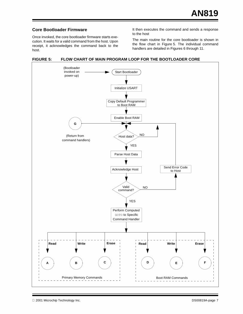
Core Bootloader Firmware
Once invoked, the core bootloader firmware starts exe-cution. It waits for a valid command from the host. Uponreceipt, it acknowledges the command back to thehost.
It then executes the command and sends a responseto the host
The main routine for the core bootloader is shown inthe flow chart in Figure 5. The individual commandhandlers are detailed in Figures 6 through 11.
FIGURE 5: FLOW CHART OF MAIN PROGRAM LOOP FOR THE BOOTLOADER CORE
Start Bootloader
Initialize USART
Copy Default Programmerto Boot RAM
Enable Boot RAM
Host data?
Parse Host Data
Acknowledge Host
Validcommand?
Send Error Codeto Host
G
Perform ComputedGOTO to Specific
Command Handler
Read Write Erase Read Write Erase
A B C D E F
Primary Memory Commands Boot RAM Commands
YES
YES
NO
NO
(Return fromcommand handlers)
(Bootloaderinvoked onpower-up)
2001 Microchip Technology Inc. DS00819A-page 7

AN819
FIGURE 6: READ COMMAND HANDLER
FIGURE 7: ERASE COMMAND HANDLER
FIGURE 8: WRITE COMMAND HANDLER
A
Initialize Data Counterand FSR at Starting
Address of Data Buffer
Read Data from Specified Address
Store Data in Buffer
Increment Address and
Alldata
read?
Send all Read Datato Host
G
Data Buffer Pointers
YES
NO
C
Transfer Control to Programmer Firmware
in Boot RAM
Chip Erasesuccessful?
G
YES
NO
Send Erase ErrorCode to Host
Send Erase SuccessCode to Host
for Chip Erase
Initialize Data Counterand FSR at Starting
Address of Data Buffer
Read Data fromData Buffer
Generate Memory LocationAddress, Byte Data andWrite Flag Information
Transfer Control toProgrammer Firmware
in Boot RAM
Writesuccessful?
All datawritten?
Send Write SuccessCode to Host
Send Write ErrorCode to Host
B
G
NO
YES
YES
NO
for Write Operation
DS00819A-page 8 2001 Microchip Technology Inc.
AN819
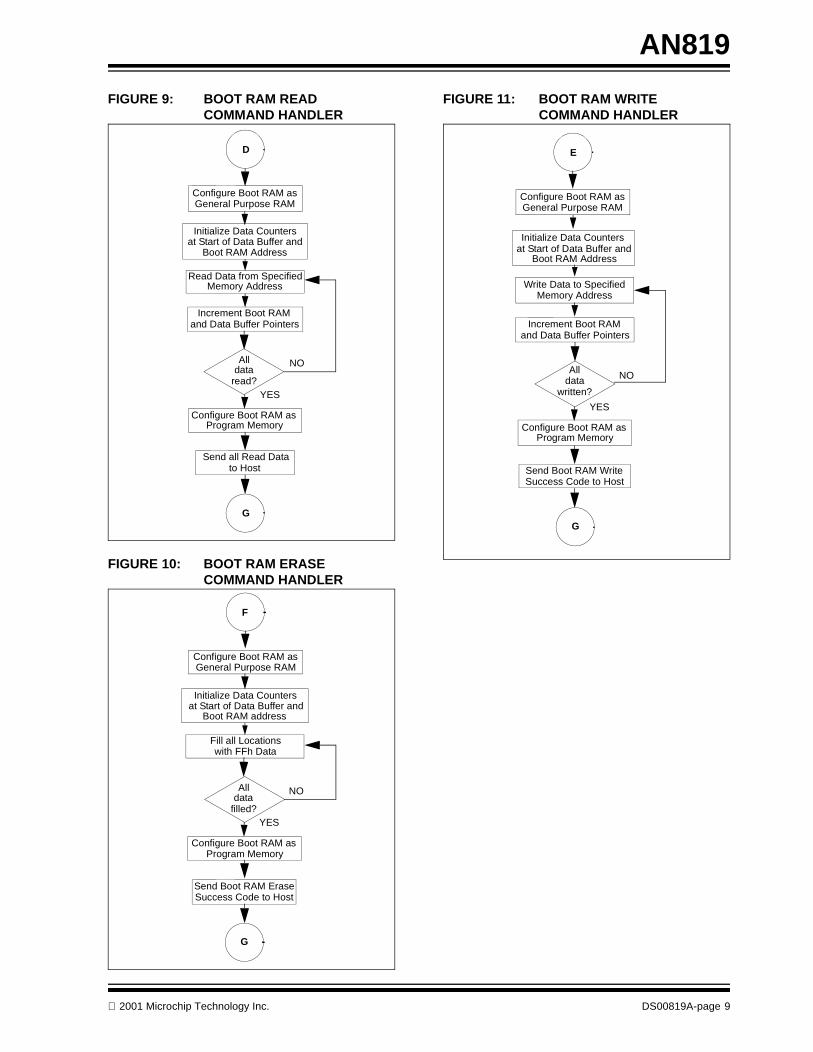
FIGURE 9: BOOT RAM READ COMMAND HANDLER
FIGURE 10: BOOT RAM ERASE COMMAND HANDLER
FIGURE 11: BOOT RAM WRITECOMMAND HANDLER
Configure Boot RAM asGeneral Purpose RAM
Initialize Data Countersat Start of Data Buffer and
Boot RAM Address
Read Data from SpecifiedMemory Address
Increment Boot RAM and Data Buffer Pointers
Alldata
read?
Configure Boot RAM asProgram Memory
Send all Read Datato Host
D
G
YES
NO
Configure Boot RAM asGeneral Purpose RAM
Initialize Data Countersat Start of Data Buffer and
Boot RAM address
Fill all Locations with FFh Data
Alldata
filled?
Configure Boot RAM asProgram Memory
Send Boot RAM EraseSuccess Code to Host
F
G
YES
NO
Configure Boot RAM asGeneral Purpose RAM
Initialize Data Countersat Start of Data Buffer and
Boot RAM Address
Write Data to SpecifiedMemory Address
Increment Boot RAMand Data Buffer Pointers
Alldata
written?
Configure Boot RAM asProgram Memory
Send Boot RAM WriteSuccess Code to Host
E
G
YES
NO
2001 Microchip Technology Inc. DS00819A-page 9

AN819
Host Software Communications
The file ‘Serial.asm’ stores the serial interface codefor a particular protocol. The ‘Serial.inc’ file con-tains definition of shared parameters for using this file.This file must be included in the “.asm” file, wherethese serial routines are used.
The ParseHostCommand function waits for a validcommand from host, and stays in the loop until a validpacket is received. It parses valid commands onreceipt, and ignores all invalid packets. A flow chart ofthis function is shown in Figure 12.
The Send Host Data functions send data to host indefined packet, while Acknowledge Host Functionacknowledges the host for command reception. A flowchart of the SendHostData is shown in Figure 13(page 11).
FIGURE 12: FLOW CHART FOR THE ParseHostCommand ROUTINE
Start
STX?
DLE?
STX?
Save Packet Length
Save Command
Save Data Byte andIncrement DataBuffer Pointer
All datareceived?
Save Checksum
Checksumverified?
DLE?
ETX?
Return toCore Bootloader
H
H
(From Core Bootloader)
DLE De-stuffing Routine
= DLE?
received
Return and
YES
YES
YES
YES
YES
YES
YES
NO
NO
NO
NO
NO
NO
NO
Is data
NO
NO
YES
YES
Wait for data;
Wait for data;
Wait for data;
Wait for Data;
Wait for Data;
Wait for Data;
Wait for Data;
Wait for data;
Wait for data;
Wait for data;
Process Data Byte
Requires DLE de-stuffing
H
DLE?
DS00819A-page 10 2001 Microchip Technology Inc.

AN819
FIGURE 13: FLOW CHART FOR THE SendHostData ROUTINE
Start
Send STX - DLE -STX Sequence
Send Packet Length;
Send Checksum
Send Extra DLE Byte
Is data= DLE?
Return toCore Bootloader
All data
sent?
YES
NO
YES
NO
DLE Stuffing Routine
(from Core Bootloader)
Initialize Checksum Value to Length
Send Command;Find new
Checksum
Send New Data;Increment Data
Send DLE-ETXSequence
Pointer, findNew Checksum
Return andSend Data Byte
Requires DLE stuffing
2001 Microchip Technology Inc. DS00819A-page 11

AN819
FIRMWARE/SOFTWARE INTERFACE
The data received by the core boot firmware will usuallycontain more than just program memory data. It willnormally also contain the address to which data is to bewritten, the number of bytes transmitted and a check-sum to detect errors. The firmware must decode, verifyand store the data, before writing it into program mem-ory. If the data is not verified, it should again ask sourceto retransmit it.
Because the available data RAM on-chip is limited incomparison to the maximum possible program size(2 MByte for the PIC18C801), the data to be pro-grammed must be divided in small blocks. The boot-loader must be able to control the reception of blocks,since it cannot process any data sent to it while it is writ-ing to its own memory. As data is transferred in blocks,an error correction mechanism to take care of transmis-sion errors becomes a requirement.
To identify transmission errors, a data communicationprotocol is required. The protocol in the referencedesign uses three instructions for the interface:
• Command, for instructions from host software to the firmware
• Acknowledge, as a “return receipt” by the firm-ware, for an instruction from the host software
• Response, containing the results of an instruction after decoding and execution by the firmware
Command Format:
<STX><DLE><Len><Command>[<Data>…]<Checksum><DLE><ETX>
where
<STX> is the “Start of TeXt” byte, used to synchro-nize the start of a packet (literal value of 02h)
<DLE> is the Data Link Escape byte, used to delimitthe frame header or footer (literal value of 04h)
<Len> is the number of data bytes in the packet
<Command> is the encoded command byte
<Data> represents the parameter byte(s) for thecommand, with a length of <Len> bytes
<Checksum> is the 8-bit 2’s complement of sum of<Len>, <Command> and <Data>
<ETX> is the “End of TeXt” byte, used to mark theend of the packet (literal value of 03h)
If the <Len>, <Command>, <Data> or <Checksum>portion of the packet resembles DLE (i.e., has a valueof 04h), an extra DLE will be stuffed before that byte.The stuffed DLEs will not change <Len> or <Check-sum> value.
The receiver of the packet verifies the integrity of thedata by adding the <Len>, <Command>, <Data> and<Checksum> bytes, excluding any stuffed DLEs. Thissum must be 00h in order to confirm the integrity ofreceived packet.
Acknowledge Format:
<STX><DLE><Len><ACK>[<Command>]<Checksum><DLE><ETX>
where
<STX> is the “Start of TeXt” byte, used to synchro-nize the start of a packet (literal value of 02h)
<DLE> is the Data Link Escape byte, used to delimitthe frame header or footer (literal value of 04h)
<ACK> is the Acknowledge byte (literal value of06h)
<Command> is the encoded command byte
<Len> is a single byte of literal value 01h
<Checksum> is the 8-bit 2’s complement of sum of<Len>, <Command> and <Data>
<ETX> is the “End of TeXt” byte, used to mark theend of the packet (literal value of 03h)
If the <Len>, <Command>, <Data> or <Checksum> por-tion of the packet resembles DLE (i.e., has a value of04h), an extra DLE will be stuffed before that byte. Thestuffed DLE(s) will not change <Len> or <Checksum>value.
The receiver of the packet verifies the integrity of thedata by adding the <Len>, <Command>, <Data> and<Checksum> bytes, excluding any stuffed DLEs. Thissum must be 00h in order to confirm the integrity ofreceived packet.
Response Format:
<STX><DLE><Len><Result>[<Data>…]<Checksum><DLE><ETX>
where
<STX> is the “Start of TeXt” byte, used to synchro-nize the start of a packet (literal value of 02h)
<DLE> is the Data Link Escape byte, used to delimitthe frame header or footer (literal value of 04h)
<Result> is the encoded binary result byte
<Data> represents the parameter byte(s) for theresult, with a length of <Len> bytes
<Checksum> is the 8-bit 2’s complement of sum of<Len>, <Command> and <Data>
<ETX> is the “End of Text” byte, used to mark theend of the packet (literal value of 03h)
If the <Len>, <Command>, <Data> or <Checksum> por-tion of the packet resembles DLE (i.e., has a value of04h), an extra DLE will be stuffed before that byte. Thestuffed DLEs will not change <Len> or <Checksum>value.
The receiver of the packet verifies the integrity of thedata by adding the <Len>, <Command>, <Data> and<Checksum> bytes, excluding any stuffed DLEs. Thissum must be 00h in order to confirm the integrity ofreceived packet.
DS00819A-page 12 2001 Microchip Technology Inc.

AN819
Table 1 lists the preliminary commands included in thereference design, as well as their parameters. Addi-tional commands can be added if and when required.
TABLE 1: BOOTLOADER FIRMWARE COMMAND SET
Command Code Parameters Response Description
RD_VER 00h Len = 0Command = RD_VER
Len = 1Result = RD_VERData[0] = Version
Returns firmware version
RD_MEM 01h Len = 5Command = RD_MEMData[0]=AddrLLData[1]=AddrLHData[2]=AddrULData[3]=AddrUHData[4]=Len
Len = 5 + LenResult = RD_MEMData[0]=AddrLLData[1]=AddrLHData[2]=AddrULData[3]=AddrUHData[4]=LenData[5…5+Len]=Memory Data
Returns memory content from given address
WR_MEM 02h Len = 6 + LenCommand = WR_MEMData[0]=AddrLLData[1]=AddrLHData[2]=AddrULData[3]=AddrUHData[4]=LenData[5]=FlagData[6..6+Len]=Data
Len = 1Result = WR_MEMData[0] = Number of bytes writ-ten
Writes given memory contents to given address
WR_CLR 03h Len=0Command = WR_CLR
Result = WR_CLRLen = 1Data[0] = Result Code‘0’ = Success‘1’ = 0 Error Code
Erases memory
RD_MEM_BOOT 0Bh Len = 5Command = RD_MEM_BOOTData[0]=AddrLLData[1]=AddrLHData[2]=AddrULData[3]=AddrUHData[4]=Len
Len = 5 + LenResult = RD_MEMData[0]=AddrLLData[1]=AddrLHData[2]=AddrULData[3]=AddrUHData[4]=LenData[5…5+Len]=Memory Data
Returns memory content from boot memory at given address
WR_MEM_BOOT 0Ch Len = 6 + LenCommand = WR_MEM_BOOTData[0]=AddrLLData[1]=AddrLHData[2]=AddrULData[3]=AddrUHData[4]=LenData[5]=FlagData[6..6+Len]=Data
Len = 1Result = WR_MEMData[0] = Number of bytes written
Writes boot memory contents to given address
WR_CLR_BOOT 0Dh Len=0Command = WR_CLR_BOOT
Result = WR_CLRLen = 1Data[0] = Result Code‘0’ = Success‘1’ = 0 Error Code
Erases boot memory
2001 Microchip Technology Inc. DS00819A-page 13

AN819
Programming Firmware
The file ‘xxx.asm’ stores the code for FLASH pro-gramming. This file is memory specific, so the user mayneed to change it depending on their specific require-ment. The default FLASH programmer can be attachedwith the bootloader; any FLASH programmer can bedownloaded on demand at a later time.
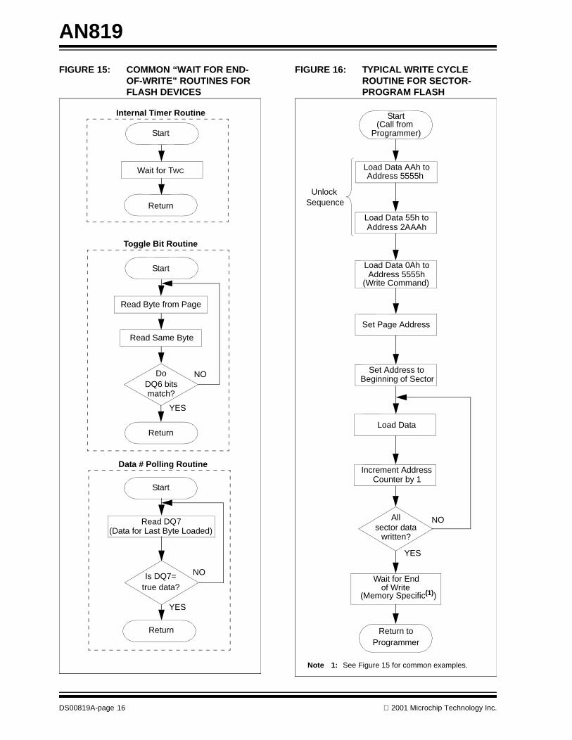
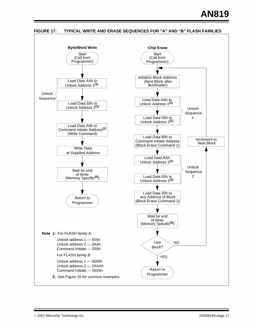
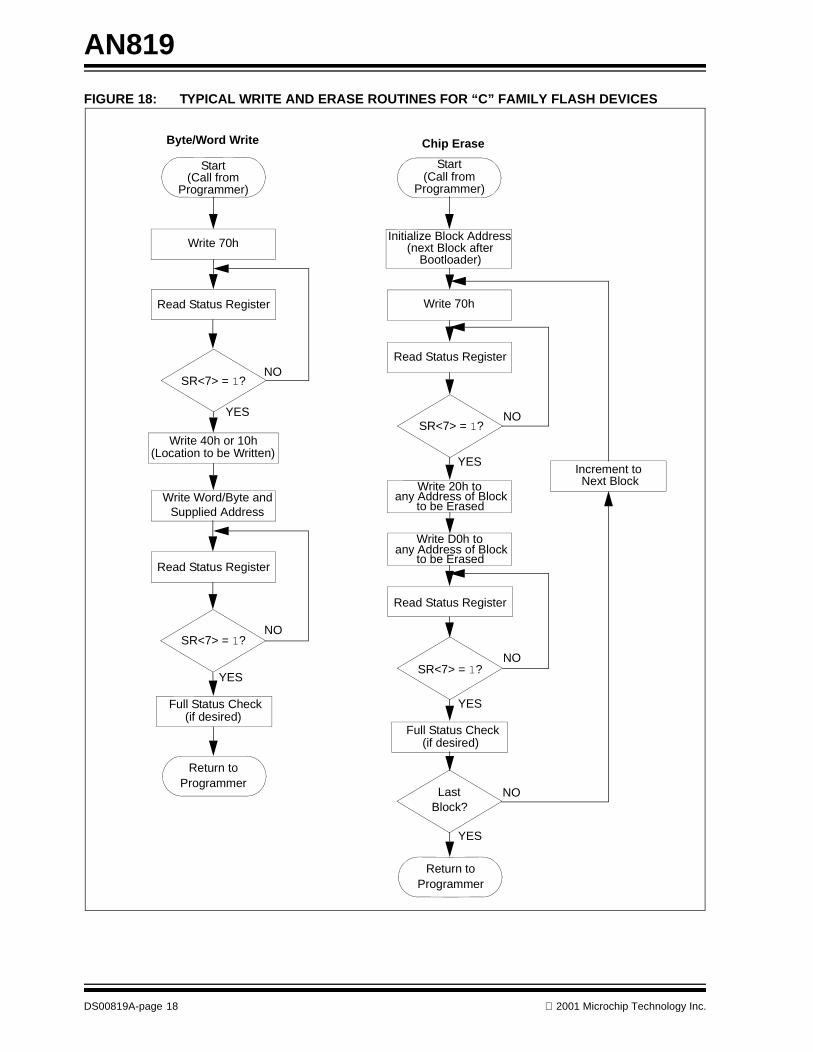
The actual implementation will vary, depending on thememory device and interface mode used. Broadly,FLASH devices can be divided into four families,depending on their programming algorithm. In additionto programming algorithm, implementation will changebased on external interface. The general programmeralgorithm is described in Figure 14. Examples ofspecific algorithms for different FLASH families areoutlined in Figures 15 through 18.
It is important to note that these flow charts do notinclude all programming algorithms for all FLASHdevice families available on the market. Additionalinformation on FLASH families and programming com-mands is provided in Appendixes C and D.
APIs FOR EXTERNAL MEMORY PROGRAMMING AND ERASE FUNCTIONS
To provide a simple method for interfacing userdesigned FLASH programming algorithms to the rest ofthe code, Application Program Interfaces (or APIs)have been designed for FLASH Erase and FLASHWrite routines. These APIs also allow the core boot-loader and programmer firmware to share information,as described later. The interfaces are described below.
Erase Function
Purpose: Erase all available memory locations.
Prototype: WREG Erase()
Input: None
Output:
WREG: Result code of this function
If WREG == 00h
Function was successful
Else
There was an error, which may beexplained by the non-zero value
Write Function
Purpose: Write an 8-bit value to a memory loca-tion defined by 32-bit value.
Prototype: WREG Write (DWORD Address,BYTE Data, BYTE Flag)
Input:
Address: 32-bit address of the location being writ-ten
Data: 8-bit data value to be written to givenaddress
Flag: Specifies whether this is a first, intermediate,last or only byte of total data to be written. The fol-lowing table describes the valid values:
Output:
WREG: Result code for this function
If WREG == 00h,
Function was successful
Else
There was an error, which may beexplained by the non-zero value
Value Meaning
00h This is the first byte being written. User may setup “Write” mode for external memory in beginning of this function.
01h This is a last byte being written. User must change external memory mode to “Read Array”.
02h This is the only byte being written. User may set up “Write” mode for external memory in beginning of this function and must change it to “Read Array” mode before returning from this function.
All other
values
This is an intermediate byte being writ-ten. User may not need to change exter-nal memory mode during this call.
DS00819A-page 14 2001 Microchip Technology Inc.

AN819
FIGURE 14: FLOW CHART FOR THE GENERAL PROGRAMMER FIRMWARE
Start
Programmer
Branch to Command ExecutorBased on Jump Table
Initialize Device(Set for TBLWT mode orDisable External Bus and
Enable I/O Ports)
Call Chip Erase Function
Initialize Device(Set for TBLWT mode or
Disable External Bus andEnable I/O Ports)
Call FLASH Write Routinefor Byte Write at Address
Evenaddress?
Make Word from this Byteand Previously Stored Byte
Call FLASH Write Routinefor Word Write to Address
Store Byte
(MSByte) is Received
ERASE WRITE
Firstbyte?
Doessupplied address
match with expectednext address?
Copy FFh into Buffer
Increment Data
Flag Address Mismatch
Allsector datareceived?
Lastbyte?
Didaddress mismatch
occur?
Initialize DataPointer Buffer
Store Address for this Data
Buffer Pointer
Copy Data into Buffer
Increment DataBuffer Pointer
Call FLASH Write Routineto Program Sector
until Odd Byte
Save pendingdata in buffer
BYTE WRITE
WORDWRITE
SECTORWRITE
NO
NO
NO
NO
NO
NO
YES
YES
YES
YES
YES
YES
Restore Device Settingsfor External Execution mode
Store Write/Erase
in W Register
Return toCommand Handlers
(Calls from various command handlers)
Success/Error Code
2001 Microchip Technology Inc. DS00819A-page 15
AN819
FIGURE 15: COMMON “WAIT FOR END-OF-WRITE” ROUTINES FOR FLASH DEVICES
FIGURE 16: TYPICAL WRITE CYCLE ROUTINE FOR SECTOR-PROGRAM FLASH
Start
Wait for TWC
Return
Internal Timer Routine
Read Byte from Page
Read Same Byte
DoDQ6 bitsmatch?
Toggle Bit Routine
Start
Return
Return
Start
Is DQ7=true data?
Read DQ7(Data for Last Byte Loaded)
Data # Polling Routine
YES
YES
NO
NO
Load Data AAh toAddress 5555h
Load Data 55h toAddress 2AAAh
Load Data 0Ah toAddress 5555h
(Write Command)
Set Page Address
Set Address toBeginning of Sector
Load Data
Increment AddressCounter by 1
Allsector data
written?
Start(Call from
Programmer)
Return toProgrammer
Wait for End
of Write(Memory Specific(1))
YES
NO
Note 1: See Figure 15 for common examples.
UnlockSequence
DS00819A-page 16 2001 Microchip Technology Inc.
AN819
FIGURE 17: TYPICAL WRITE AND ERASE SEQUENCES FOR “A” AND “B” FLASH FAMILIES
UnlockSequence
UnlockSequence
UnlockSequence
Byte/Word Write Chip Erase
Load Data AAh toUnlock Address 1(1)
Load Data 55h toUnlock Address 2(1)
Load Data A0h toCommand Initiate Address(1)
(Write Command)
Write Data
Return toProgrammer
Start(Call from
Programmer)
Start(Call from
Programmer)
Initialize Block Address(Next Block after
Bootloader)
Load Data AAh to
Load Data 55h toUnlock Address 2(1)
Unlock Address 1(1)
Load Data 80h toCommand Initiate Address(Block Erase Command 1)
Load Data AAh Unlock Address 1(1)
Load Data 55h toUnlock Address 2(1)
Load Data 30h toany Address of Block
(Block Erase Command 2)
LastBlock?
Note 1: For FLASH family A:
Unlock address 1 — 555hUnlock address 2 — 2AAhCommand Initiate — 555h
For FLASH family B:
Unlock address 1 — 5555hUnlock address 2 — 2AAAhCommand Initiate — 5555h
2: See Figure 15 for common examples.
1
2
Increment toNext Block
Return toProgrammer
YES
NO
at Supplied Address
Wait for end
of Write(Memory Specific(2))
Wait for endof Write
(Memory Specific(2))
2001 Microchip Technology Inc. DS00819A-page 17
AN819
FIGURE 18: TYPICAL WRITE AND ERASE ROUTINES FOR “C” FAMILY FLASH DEVICES
Byte/Word Write Chip Erase
Start(Call from
Programmer)
Start(Call from
Programmer)
Write 70h
Read Status Register
SR<7> = 1?
Write 40h or 10h(Location to be Written)
Write Word/Byte andSupplied Address
SR<7> = 1?
Read Status Register
Full Status Check(if desired)
Return toProgrammer
Return toProgrammer
Initialize Block Address(next Block after
Bootloader)
Write 70h
Read Status Register
Read Status Register
SR<7> = 1?
SR<7> = 1?
Write 20h toany Address of Block
Write D0h toany Address of Block
Full Status Check(if desired)
LastBlock?
Increment toNext Block
YES
YES
YES
YES
YES
NO
NO
NO
NO
NO
to be Erased
to be Erased
DS00819A-page 18 2001 Microchip Technology Inc.

AN819
PARAMETER PASSING MECHANISM FOR ASSEMBLY LANGUAGE
Normally, the default flash programmer is attached withthe core bootloader; an alternate programmer can bedownloaded from the host software later, if required.This ability to change programmer firmware is why thethe core bootloader and programmer are built as sepa-rate projects. In doing this, however, it becomes neces-sary to provide a mechanism for sharing data andfunctions between the two. It is also essential to pre-vent the firmware components from using overlappingareas of RAM. This can best be done by using an abso-lute addressing scheme.
To enforce reasonable type checking, the generic codeportion will define and export certain variables. Theseare listed in Example 1.
Generic code will populate these variables before call-ing user supplied Write function. The user suppliedWrite function will import these variables and use themas needed.
WRITING NEW FLASH MEMORY ROUTINES FOR THE BOOTLOADER
User supplied Write functions can use the provided‘memrtnes.inc’ file, which contains the definition ofthese parameters, as shown in Example 2. This way,the core bootloader and programmer firmware canshare the data.
If memory routines are built separately from the boot-loader, always use the “memrtnes.lkr” file (includedin the Zip archive available at the Microchip website) tobuild them. This makes sure that the FLASH routinesdo not overlap with monitor data RAM area.
Now that a system for sharing the data is established,we need a mechanism to share the functions as well.One solution is to fix the location for Write and Erasefunctions themselves. This may create a problem if allthe required firmware does not fit in the allotted space.We need some mechanism, so a user can place theirfirmware at anywhere in available area. FLASH pro-grammer specific code contains a “jump table” at thebeginning of code, which is what the bootloader uses tocall appropriate routines. This jump table allows user tolocate their actual functions anywhere in the 512-bytearea; they do not have to “origin” their functions at hardcoded addresses. When FLASH routines are down-loaded by the host software, it “relocates” them atbeginning of Boot RAM; for this reason, users mustonly use bra and rcall instructions for jumps.Example 3 shows how this is done.
The best way to embed the memory routine code is touse the template file “memrtnes.tpl”, which takescare of all the definitions. The template is also includedin the Zip archive available at the Microchip website.
EXAMPLE 1: DEFINING COMMON VARIABLES FOR PASSING PARAMETERS
EXAMPLE 2: EXAMPLE CODE FOR memrtnes.inc
Note: For more information on using the tem-plates, please refer to the User’s Manualand on-line help for the MPLAB® develop-ment system.
UDATA_ACS .00Address RES .04 ; Parameter #1 for Write functionByte RES .01 ; Parameter #2 for Write functionFlags RES .01 ; Parameter #3 for Write function
Address EQU .00 ; 32 bit Address of the location being writtenByte EQU .04 ; 8-bit data value to be written Flags EQU .05 ; Specifies whether this is a first,
; intermediate, last or only one byte of; total data to be written
2001 Microchip Technology Inc. DS00819A-page 19

AN819
EXAMPLE 3: PROVIDING FOR RELOCATABLE WRITE AND ERASE FUNCTIONS
INTEGRATING THE BOOTLOADER WITH USER CODE
The bootloader code usually uses the RESET locationand some additional program memory. It can also usethe interrupt; but, if an interrupt occurs while the codeis executing from Boot RAM, it will jump to the interruptservice vector in FLASH program memory. This couldbe dangerous if programming the new code into exter-nal memory has not been completed. Thus, the on-board programmer must not use interrupt driven code.It should disable interrupts until it finishes programmingexternal memory.
The bootloader starts at the RESET location. To avoidaccidental erasure, this entire sector of program mem-ory must be protected. As the interrupt vector also fallsin this range, the bootloader must relocate it. Addition-ally, the bootloader must know where the applicationcode starts, to be able to execute it. Similarly, users maywant to change other bootloader related configurationitems for different systems, such as the pin monitored toinvoke the firmware, or the oscillator frequency used tocalculate the baud rate for serial communications.
All of these user code related parameters are definedin the ‘UserCode.inc’ file. Users can edit this file toquickly modify the firmware to suit their particularrequirements. An example is shown in Example 4(page 21). Users should store their code in the nextsector after the Bootloader code. This location addressis defined in the UserCode label. In the same fashion,interrupt vector relocation addresses are defined at‘HighPriorIntServ’ and ‘LowPriorIntServ’ , for high
priority and low priority Interrupt Service Routines,respectively. The pin monitored for bootloader invoca-tion is defined by BootLoadChkPin . Both the Portname and bit number should be defined here.
The bootloader code coexists with the user code on thedevice and many of the resources used by the bootcode can also be used by the user code. The core boot-loader and programmer firmware uses the resourceslisted in Table 2.
TABLE 2: RESOURCES NEEDED FOR THE BOOTLOADER
Bootloader Code section for Calling Write and Erase APIs
call 1FFE00h + @Command ;Write Command =0, Erase Command=2
In this instance, the FLASH Write function called is located at 1FFE00h, while the Erase function is located at1FFE02h. The command handler must be located at these locations. This is done as follows:
Programmer CODE ;This section when copied to Boot RAM makes address 1FFE00bra Write ;Branch to Write functionbra Erase ;Branch to Erase function
Write:
;(Insert Write routine here)
return
Erase:
;(Insert Erase routine here)
return
Resource
Bootloader Requirements
Core BootFirmware
ProgrammerFirmware*
Program memory(bytes)
1024 Up to 512
Data memory (access RAM, bytes)
32 0 to 3
Data memory(general purpose RAM, bytes)
255 Up to 512
I/O pins 1 System Bus or I/O pins
Peripherals USART Generally none
* Requirements vary by specific implementation and FLASH programming algorithm.
DS00819A-page 20 2001 Microchip Technology Inc.

AN819
EXAMPLE 4: SAMPLE UserCode.inc CONFIGURATION FILE
The program memory used by the bootloader cannotbe used for user code. However, actual memory con-sumption will depend on the sector size, as the sectorcontaining bootloader code must be protected (andtherefore, cannot contain user code). Larger sectorsizes mean greater memory consumption; smaller sec-tors mean lesser consumption. As the bootloader firm-ware can consume significant data memory resources,it is not likely that developers will want to reserve theseon an ongoing basis for code that is infrequently called.As all the code is written in relocatable format,MPLINKTM Object Linker will not allow the re-use ofresources used by the bootloader code, if applicationcode is merged with bootloader code to make a singleproject. Therefore, combining user code and boot-loader code into a single project should be avoided.
In a production environment, however, it is desirable toprogram the entire FLASH device with the bootloaderfirmware and user application code in a single shot. Inthis case, the developer should build two separate HEXfiles (bootloader and user code), then merge the two tocreate a single HEX file. This allows the developer tore-use the data memory resources used by the boot-loader.
To avoid overlap of program memory, the developershould use the appropriate linker script file. User codeshould use a linker script file similar to the one shownin Figure 5. This will prevent overlap of user code withBootloader. The text in bold defines the sector require-ment. The text in bold italics shows the maximumavailable program memory with device; this is modifiedaccording to the physical memory connected to thedevice. If more than one memory device is connected,this file should reflect memory map of the system. Theuse of a proper linker script file will ensure that thelinker places code and variables in the proper places.
The USART can be used by the user code. Any I/Opin(s) monitored to invoke the bootloader can be usedas an output, by isolating their switches or jumpers witha resistor.
In summary, all resources used by the bootloader,except program memory, can also be used by the userapplication code. Figure 19 shows the final combinedmemory map of user code and bootloader firmware.
EXAMPLE 5: SAMPLE LINKER SCRIPT FILE
UserCode EQU 0x1000 ;User Code jump locationHighPriorIntServ EQU 0x1008 ;Higher priority interrupt
;service routine jump locationLowPriorIntServ EQU 0x1018 ;Lower priority interrupt
;service routine jump location#define BootLoadChkPin PORTF,2 ;Boot load Checking port pin numberFOSC EQU D’16000000’ ;Oscillator Frequency
Note: Users can merge HEX files by using thefacilities available in some programmers.
Note: For additional information on linker scripts,please refer to the Microchip MPLINKUser’s guide.
// File: UserCode.lkr// Sample linker command file for User code
LIBPATH .
CODEPAGE NAME=vectors START=0x0 END=0x29 PROTECTEDCODEPAGE NAME=Bootloader START=0x2A END=0xFFF PROTECTEDCODEPAGE NAME=page START=0x1000 END=0x200000CODEPAGE NAME=config START=0x300000 END=0x300007 PROTECTEDCODEPAGE NAME=idlocs START=0x3FFFFE END=0x3FFFFF PROTECTED
ACCESSBANK NAME=accessram START=0x0 END=0x7FDATABANK NAME=gpr0 START=0x80 END=0xFFDATABANK NAME=gpr1 START=0x100 END=0x1ffDATABANK NAME=gpr2 START=0x200 END=0x2FFDATABANK NAME=gpr3 START=0x300 END=0x3FFDATABANK NAME=gpr4 START=0x400 END=0x4FFDATABANK NAME=gpr5 START=0x500 END=0x5FFDATABANK NAME=sfr START=0xF00 END=0xF7F PROTECTEDACCESSBANK NAME=accesssfr START=0xF80 END=0xFFF PROTECTED
2001 Microchip Technology Inc. DS00819A-page 21

AN819
FIGURE 19: MEMORY MAP FOR COMBINED BOOTLOADER AND USER CODE
CONCLUSION
Incorporating bootloader firmware into a micro-controller based design allows for easy and efficientfield upgrades of a product, which in turn, can enhanceits functionality and value. Designs using thePIC18C601/801 ROMless microcontrollers can easilyincorporate a bootloader to enhance their flexibility.
The reference design demonstrated in this note pro-vides a flexible and modular framework for bootloaderfirmware. To recap, some of the features included are:
• External host software with a simple GUI and the flexibility to handle the most popular HEX file formats
• A serial communications interface with a robust data communication protocol, making it possible to identify and correct communication errors
• Downloadable programmer firmware, which allows for the development and substitution of new FLASH programming algorithms
• Prewritten linker scripts, templates, and “include” files for the efficient development of new memory routines, the ability to share device resources and overlap multiple code pieces, and the ability to customize the firmware to user requirements
• The ability to map the external bus to I/O ports, to allow the implementation of any memory pro-gramming algorithm
Using the key components of the reference design willallow developers to create their own custom bootloaderfirmware, specifically tailored to their application’sresources and requirements.
Relocated User Interrupt Code
Bootloader Code
Boot RAM(when PGRM = ‘1’)
UserApplication
Code
0000h
1FFE00h
1FFFFFh
Protected sectorcontaining boot code
Note: Sizes of code areas not shown to scale.
DS00819A-page 22 2001 Microchip Technology Inc.

AN819
APPENDIX A: REFERENCES
Readers with additional questions on Microchip ROM-less microcontrollers, the external memory interfaceand FLASH memory programming, are referred to thedocuments listed below for more information. Theymay be downloaded from the Microchip corporate web-site, at
www.microchip.com
• DS39541, “PIC18C601/801 Data Sheet”• DS00778, “Implementing the External Memory
Interface on PIC18C601/801 MCUs”
APPENDIX B: SOFTWARE DISCUSSED IN THIS APPLICATION NOTE
Because of the overall length of all components, a com-plete source file listing for the bootloader referencedesign is not provided. Those users who are interestedin further exploring the bootloader firmware are encour-aged to download the project files for their examination.
The software discussed in this application note (theHost Software executable file and project files and tem-plates for the bootloader firmware) are available as asingle WinZip archive file. The archive may be down-loaded from the Microchip corporate Web site at:
www.microchip.com
2001 Microchip Technology Inc. DS00819A-page 23

AN819
APPENDIX C: SUMMARY OF MEMORY DEVICES(1)
Manufacturer Part IDProgramming
Algorithm Family(2)
OrganizationBasic
Byte/WordAddressing(4)
Remarks
AMD 29F series A x8
29F series A x16
29F series A x8/x16 Byte
ATMEL 29 Series29 Series
B(3)
B(3)x8
x16Sector Programming
49 Series B x8
49 Series B x16
49 Series B x8/x16 Byte
INTEL Boot Block C x8/x16 Byte
Strata FLASH/ FLASH File
C x8
Strata FLASH/ FLASH File
C x8/x16 Word
SHARP 28F series C x8
28F series C x16
28F series C x8/x16 Word
ST 29F series A x8
29F series A x16
29F series A x8/x16 Byte
Samsung FLASH products in this family have multiplexed address/data/command lines, and are incompatible with PIC18C601/801 devices.
Catalyst Boot Block FLASH
C x8
Bulk Erase FLASH
(5) x8x16
Note 1: This listing is provided only as an example of typical memory devices available. It is not meant to be exhaustive.
2: Details of each programming algorithm family are provided in Appendix B.3: For these devices, users must provide all data in the sector. The device will first erase the entire sector, then
program it. These devices do not support Sector Erase commands.4: Applicable only to x8/x16 selectable devices.5: These devices have a unique set of programming algorithms. They are omitted for the sake of brevity.
DS00819A-page 24 2001 Microchip Technology Inc.

AN819
Hyundai 29F series A x8
29F series A x8/x16 Byte
Micron Boot Block C x8
Boot Block C x8/x16 Byte
Even Sectored
C x8
Even Sectored
C x8/x16 Word
SST 39F Series B x8
29EE Series B(3) x8 Sector Programming
NexFlash 29F series B x8
APPENDIX C: SUMMARY OF MEMORY DEVICES(1) (CONTINUED)
Manufacturer Part IDProgramming
Algorithm Family(2)
OrganizationBasic
Byte/WordAddressing(4)
Remarks
Note 1: This listing is provided only as an example of typical memory devices available. It is not meant to be exhaustive.
2: Details of each programming algorithm family are provided in Appendix B.3: For these devices, users must provide all data in the sector. The device will first erase the entire sector, then
program it. These devices do not support Sector Erase commands.4: Applicable only to x8/x16 selectable devices.5: These devices have a unique set of programming algorithms. They are omitted for the sake of brevity.
2001 Microchip Technology Inc. DS00819A-page 25

AN819
APPENDIX D: PROGRAMMING ALGORITHMS FOR REPRESENTATIVE MEMORY DEVICES(1)
Command Program
Algorithm
Bus Cycles
Cycles needed
First Second Third Fourth Fifth Sixth
Addr Data Addr Data Addr Data Addr Data Addr Data Addr Data
Read mode/RESET
A 1 X F0 — — — — — — — — — —
B 1 X F0 — — — — — — — — — —
C 1 X FF — — — — — — — — — —
Read Mfg. ID
A 4 555 AA 2AA 55 555 90 X00 01 — — — —
B 4 5555 AA 2AAA 55 5555 90 XX00 01 — — — —
C 2 X 90 (IA) (ID) — — — — — — — —
ReadDevice ID
A 4 555 AA 2AA 55 555 90 X01 AD — — — —
B 4 5555 AA 2AAA 55 5555 90 XX01 20 — — — —
C 2 X 90 (IA) (ID) — — — — — — — —
Write A 4 555 AA 2AA 55 555 A0 (WA) (WD) — — — —
B 4 5555 AA 2AAA 55 555 A0 (WA) (WD) — — — —
C 2 (WA) 40 (WA) (WD) — — — — — — — —
Block Erase
A 6 555 AA 2AA 55 555 80 555 AA 2AA 55 (BA) 30
B 6 5555 AA 2AAA 55 5555 80 5555 AA 2AAA 55 (BA) 30
C 2 (BA) 20 (BA) D0 — — — — — — — —
Erase Suspend
A 1 X B0 — — — — — — — — — —
B (2)
C 1 X B0 — — — — — — — — — —
Erase Resume
A 1 X 30 — — — — — — — — — —
B (2)
C 1 X D0 — — — — — — — — — —
Chip Erase A 6 555 AA 2AA 55 555 80 555 AA 2AA 55 555 10
B 6 5555 AA 2AAA 55 5555 80 5555 AA 2AAA 55 5555 10
C 2 X 30 X D0 — — — — — — — —
Sector Protect Verify
A 4 555 AA 2AA 55 555 90 (SGA) 00/01 — — — —
B 4 5555 AA 2AAA 55 5555 90 (SGA) 00/01 — — — —
C (2)
Legend: WA = Write Address, WD = Write Data, IA = Identifier Address, ID = Identifier Data,BA = Block Address, SGA = Sector Group Address, X = Don’t Care
Note 1: The information provided in this table is for reference only, and is not meant to be a comprehensive description of the device programming algorithms. For complete information, please refer to the manufacturer’s data sheet.
2: Instruction unimplemented in this programming algorithm family.
DS00819A-page 26 2001 Microchip Technology Inc.

AN819
APPENDIX E: THE HOST SOFTWARE WINDOW
As previously described, the host software for the ref-erence design bootloader is implemented using a sin-gle window (Figure E-1). All commands are availablefrom both the menu bar; most are also available fromeither the icon-based toolbar (Figure E-2), or keyboardshortcuts. File commands (New, Open, Save, etc.)invoke the standard Windows dialog boxes for file loca-tion, name and file format. A complete summary of allavailable commands is given in Table E-1.
Also available on the Tool Bar is the option to changethe COM port setting used by the host system to com-municate with the target. The selector is not duplicatedas a command menu option. The default port is COM1.
It is important to note that the host software is not aHEX file editor; the display in the main window onlyshows the current HEX file or memory device contentsloaded into the buffer. Developers who want to makechanges to a programmed device will still need to fol-low the usual steps of the software development cycle,using the appropriate software tools for code designand compilation to a HEX file. Only then can the HEXfile be loaded into the host software and reprogrammedinto the device.
FIGURE E-1: HOST SOFTWARE WINDOW
FIGURE E-2: HOST SOFTWARE TOOLBAR
New
Open
Save
Program
Read
Write
Verify Abort (available during
Erase
Download Memory Routines
COM Port Selector
operations only)
2001 Microchip Technology Inc. DS00819A-page 27

AN819
TABLE E-1: SUMMARY OF HOST SOFTWARE COMMANDS
Menu CommandKeyboardShortcut
Description
File New <Ctrl-N> Clears the host software buffer and prepares for a new HEX file to be loaded.
Open <Ctrl-O> Opens an existing Intel HEX file residing on the host sys-tem and displays it in the main window. The software will prompt for the file name and its location.
Close — Closes the currently open HEX file and clears the host software buffer. If changes have occurred and have not been saved, the user will be asked if they wish to save the changes.
Save <Ctrl-S> Saves the currently displayed data to the open HEX file. If no HEX file is open, invokes the “Save As” function.
Save As <F12> Save the currently displayed data as an Intel HEX file. A dialog box will prompt for location and new file name.
Exit — Exit the host software without changing or saving the cur-rently displayed data.
Operation Program <Ctrl-P> Programs the contents of the host software buffer to the target memory device. For FLASH devices, this includes erasing the target, writing to the target, then verifying the data written.
Write <Ctrl-W> Downloads the current contents of the host software buffer to the target device, without performing Erase or Verify operations.
Read <Ctrl-R> Reads the code from the target memory device and dis-plays it in the main window. The software will prompt for a range of addresses to be read.
Erase <Ctrl-E> Erases the target memory device.
Verify <Ctrl-V> Verifies the current contents of the memory device against the displayed file.
Download Memory Routines <Ctrl-M> Downloads the contents of the host software buffer to Boot RAM of the target controller, and verifies after download.
Read Memory Routines — Reads the current contents of Boot RAM from the target controller, and displays it in the main window.
Verify Memory Routines — Verifies the current contents of Boot RAM against the dis-played file.
Abort <Ctrl-A> Terminates the current operation.
Help About — Displays the current revision of the host software.
Note: Interrupting a Program or Write operation with the Abort command can cause unpredictable memory states,which may result in erratic operation. This may require erasing and reprogramming the target memorydevice.
DS00819A-page 28 2001 Microchip Technology Inc.

Note the following details of the code protection feature on PICmicro® MCUs.
• The PICmicro family meets the specifications contained in the Microchip Data Sheet.• Microchip believes that its family of PICmicro microcontrollers is one of the most secure products of its kind on the market today,
when used in the intended manner and under normal conditions.• There are dishonest and possibly illegal methods used to breach the code protection feature. All of these methods, to our knowl-
edge, require using the PICmicro microcontroller in a manner outside the operating specifications contained in the data sheet. The person doing so may be engaged in theft of intellectual property.
• Microchip is willing to work with the customer who is concerned about the integrity of their code.• Neither Microchip nor any other semiconductor manufacturer can guarantee the security of their code. Code protection does not
mean that we are guaranteeing the product as “unbreakable”.• Code protection is constantly evolving. We at Microchip are committed to continuously improving the code protection features of
our product.
If you have any further questions about this matter, please contact the local sales office nearest to you.
Information contained in this publication regarding deviceapplications and the like is intended through suggestion onlyand may be superseded by updates. It is your responsibility toensure that your application meets with your specifications.No representation or warranty is given and no liability isassumed by Microchip Technology Incorporated with respectto the accuracy or use of such information, or infringement ofpatents or other intellectual property rights arising from suchuse or otherwise. Use of Microchip’s products as critical com-ponents in life support systems is not authorized except withexpress written approval by Microchip. No licenses are con-veyed, implicitly or otherwise, under any intellectual propertyrights.
2001 Microchip Technology Inc.
Trademarks
The Microchip name and logo, the Microchip logo, FilterLab,KEELOQ, MPLAB, PIC, PICmicro, PICMASTER, PICSTART,PRO MATE, SEEVAL and The Embedded Control SolutionsCompany are registered trademarks of Microchip TechnologyIncorporated in the U.S.A. and other countries.
dsPIC, ECONOMONITOR, FanSense, FlexROM, fuzzyLAB,In-Circuit Serial Programming, ICSP, ICEPIC, microID,microPort, Migratable Memory, MPASM, MPLIB, MPLINK,MPSIM, MXDEV, PICC, PICDEM, PICDEM.net, rfPIC, SelectMode and Total Endurance are trademarks of MicrochipTechnology Incorporated in the U.S.A.
Serialized Quick Term Programming (SQTP) is a service markof Microchip Technology Incorporated in the U.S.A.
All other trademarks mentioned herein are property of theirrespective companies.
© 2001, Microchip Technology Incorporated, Printed in theU.S.A., All Rights Reserved.
Printed on recycled paper.
DS00819A - page 29
Microchip received QS-9000 quality system certification for its worldwide headquarters, design and wafer fabrication facilities in Chandler and Tempe, Arizona in July 1999. The Company’s quality system processes and procedures are QS-9000 compliant for its PICmicro® 8-bit MCUs, KEELOQ® code hopping devices, Serial EEPROMs and microperipheral products. In addition, Microchip’s quality system for the design and manufacture of development systems is ISO 9001 certified.

DS00819A-page 30 2001 Microchip Technology Inc.
MAMERICASCorporate Office2355 West Chandler Blvd.Chandler, AZ 85224-6199Tel: 480-792-7200 Fax: 480-792-7277Technical Support: 480-792-7627Web Address: http://www.microchip.comRocky Mountain2355 West Chandler Blvd.Chandler, AZ 85224-6199Tel: 480-792-7966 Fax: 480-792-7456
Atlanta500 Sugar Mill Road, Suite 200BAtlanta, GA 30350Tel: 770-640-0034 Fax: 770-640-0307Boston2 Lan Drive, Suite 120Westford, MA 01886Tel: 978-692-3848 Fax: 978-692-3821Chicago333 Pierce Road, Suite 180Itasca, IL 60143Tel: 630-285-0071 Fax: 630-285-0075Dallas4570 Westgrove Drive, Suite 160Addison, TX 75001Tel: 972-818-7423 Fax: 972-818-2924DaytonTwo Prestige Place, Suite 130Miamisburg, OH 45342Tel: 937-291-1654 Fax: 937-291-9175DetroitTri-Atria Office Building 32255 Northwestern Highway, Suite 190Farmington Hills, MI 48334Tel: 248-538-2250 Fax: 248-538-2260Kokomo2767 S. Albright Road Kokomo, Indiana 46902Tel: 765-864-8360 Fax: 765-864-8387Los Angeles18201 Von Karman, Suite 1090Irvine, CA 92612Tel: 949-263-1888 Fax: 949-263-1338New York150 Motor Parkway, Suite 202Hauppauge, NY 11788Tel: 631-273-5305 Fax: 631-273-5335San JoseMicrochip Technology Inc.2107 North First Street, Suite 590San Jose, CA 95131Tel: 408-436-7950 Fax: 408-436-7955Toronto6285 Northam Drive, Suite 108Mississauga, Ontario L4V 1X5, CanadaTel: 905-673-0699 Fax: 905-673-6509
ASIA/PACIFICAustraliaMicrochip Technology Australia Pty LtdSuite 22, 41 Rawson StreetEpping 2121, NSWAustraliaTel: 61-2-9868-6733 Fax: 61-2-9868-6755China - BeijingMicrochip Technology Consulting (Shanghai)Co., Ltd., Beijing Liaison OfficeUnit 915Bei Hai Wan Tai Bldg.No. 6 Chaoyangmen Beidajie Beijing, 100027, No. ChinaTel: 86-10-85282100 Fax: 86-10-85282104China - ChengduMicrochip Technology Consulting (Shanghai)Co., Ltd., Chengdu Liaison OfficeRm. 2401, 24th Floor, Ming Xing Financial TowerNo. 88 TIDU StreetChengdu 610016, ChinaTel: 86-28-6766200 Fax: 86-28-6766599China - FuzhouMicrochip Technology Consulting (Shanghai)Co., Ltd., Fuzhou Liaison OfficeRm. 531, North BuildingFujian Foreign Trade Center Hotel73 Wusi RoadFuzhou 350001, ChinaTel: 86-591-7557563 Fax: 86-591-7557572China - ShanghaiMicrochip Technology Consulting (Shanghai)Co., Ltd.Room 701, Bldg. BFar East International PlazaNo. 317 Xian Xia RoadShanghai, 200051Tel: 86-21-6275-5700 Fax: 86-21-6275-5060China - ShenzhenMicrochip Technology Consulting (Shanghai)Co., Ltd., Shenzhen Liaison OfficeRm. 1315, 13/F, Shenzhen Kerry Centre,Renminnan LuShenzhen 518001, ChinaTel: 86-755-2350361 Fax: 86-755-2366086Hong KongMicrochip Technology Hongkong Ltd.Unit 901-6, Tower 2, Metroplaza223 Hing Fong RoadKwai Fong, N.T., Hong KongTel: 852-2401-1200 Fax: 852-2401-3431IndiaMicrochip Technology Inc.India Liaison OfficeDivyasree Chambers1 Floor, Wing A (A3/A4)No. 11, O’Shaugnessey RoadBangalore, 560 025, IndiaTel: 91-80-2290061 Fax: 91-80-2290062
JapanMicrochip Technology Japan K.K.Benex S-1 6F3-18-20, ShinyokohamaKohoku-Ku, Yokohama-shiKanagawa, 222-0033, JapanTel: 81-45-471- 6166 Fax: 81-45-471-6122KoreaMicrochip Technology Korea168-1, Youngbo Bldg. 3 FloorSamsung-Dong, Kangnam-KuSeoul, Korea 135-882Tel: 82-2-554-7200 Fax: 82-2-558-5934SingaporeMicrochip Technology Singapore Pte Ltd.200 Middle Road#07-02 Prime CentreSingapore, 188980Tel: 65-334-8870 Fax: 65-334-8850TaiwanMicrochip Technology Taiwan11F-3, No. 207Tung Hua North RoadTaipei, 105, TaiwanTel: 886-2-2717-7175 Fax: 886-2-2545-0139
EUROPEDenmarkMicrochip Technology Nordic ApSRegus Business CentreLautrup hoj 1-3Ballerup DK-2750 DenmarkTel: 45 4420 9895 Fax: 45 4420 9910FranceMicrochip Technology SARLParc d’Activite du Moulin de Massy43 Rue du Saule TrapuBatiment A - ler Etage91300 Massy, FranceTel: 33-1-69-53-63-20 Fax: 33-1-69-30-90-79GermanyMicrochip Technology GmbHGustav-Heinemann Ring 125D-81739 Munich, GermanyTel: 49-89-627-144 0 Fax: 49-89-627-144-44ItalyMicrochip Technology SRLCentro Direzionale Colleoni Palazzo Taurus 1 V. Le Colleoni 120041 Agrate BrianzaMilan, Italy Tel: 39-039-65791-1 Fax: 39-039-6899883United KingdomArizona Microchip Technology Ltd.505 Eskdale RoadWinnersh TriangleWokingham Berkshire, England RG41 5TUTel: 44 118 921 5869 Fax: 44-118 921-5820
10/01/01
WORLDWIDE SALES AND SERVICE


![Atmel AT03030: QMatrix Touchpad – 2D Position …ww1.microchip.com/downloads/en/AppNotes/Atmel-42202...Atmel AT03030: QMatrix Touchpad – 2D Position Tracking [APPLICATION NOTE]](https://img.pdfslide.us/doc/110x75/5e82bfb366844315cb3c3385/atmel-at03030-qmatrix-touchpad-a-2d-position-ww1-atmel-at03030-qmatrix.jpg)