Embed Size (px)
Citation preview
AN1631Simple Link Budget Estimation and Performance Measurements
of Microchip Sub-GHz Radio Modules
Author: Pradeep ShamannaMicrochip Technology Inc.
INTRODUCTION
The increased popularity of short range wireless in home, building and industrial applications with Sub-GHz (<1 GHz) band requires the system designers to understand the methods, estimation, cost and trade-off in short range wireless communication. Apart from considering the range estimation formula, it is good to understand the wireless channel and propagation environment involved with Sub-GHz. Generally, RF/wireless engineers perform a link budget while starting an RF design. The link budget considers range, transmit power, receiver sensitivity, antenna gains, frequency, reliability, propagation medium (which includes the principles of physics linked to reflection, diffraction and scattering of electromagnetic waves), and environment factors to accurately calculate the performance of a Sub-GHz RF radio link.
Sub-GHz wireless networks can provide cost-effective solutions in any low data rate system, from simple point-to-point connections to much larger mesh networks, where long range, robust radio links and extended battery life are priorities. Higher regulatory output power, reduced absorption, less spectral pollution and narrow band operation increase the transmission range. Improved signal propagation, good circuit design, and lesser memory space usage can reduce the power consumption; hence support longer battery life.
Usually, Sub-GHz channels are part of unlicensed Industrial Scientific Medical (ISM) frequency bands. Sub-GHz nodes generally target low-cost systems, with each node costing approximately 30% to 40% less compared to the advanced wireless systems and uses less stack memory. Many protocols such as IEEE 802.15.4 based ZigBee® (currently, the only protocol offering both 2.4 GHz and Sub-GHz versions in the 868 MHz and 900 MHz bands), automation protocols, cordless phones, Wireless Modbus, Remote Keyless Entry (RKE), Tire Pressure Monitoring System (TPMS) and lot of proprietary protocols (including MiWi™), occupy this band. However, operation in the Sub-GHz ISM band induces the radios to interfere with other protocols utilizing the same spectrum which includes threat from mobile phones, licensed cordless phones, and so on.
This application note describes a simple link budget analysis, measurement and techniques to evaluate the range and performance of wireless transmission with results, and uses developed models to estimate the path loss for short range Microchip Sub-GHz modules using MRF89XA and MRF49XA radios both for indoor and outdoor environment. Hence, an attempt is made to provide designers with an initial estimate on wireless communication system’s performance. The performance parameters include range, path loss, receiver sensitivity and Bit Error Rate (BER)/Packet Error Rate (PER) parameters which are critical in any communication.
The MRF89XAM8A (for 868 MHz band) and MRF89XAM9A (for 915 MHz band) modules based on MRF89XA transceivers, the MRF49XA-433 MHz, MRF49XA-868 MHz, and MRF49XA-915 MHz PICtail boards based on the MRF49XA transceivers, have varied specifications relating to power, type of antenna, and gain. These modules are considered for measurement purpose in this application note.
2013 Microchip Technology Inc. DS00001631A-page 1
AN1631
LINK BUDGET
Link budget is the accounting of all gains and losses from the transmitter (TX) through the medium (free space) to the receiver (RX) in a wireless communication system. Link budget considers the parameters that decide the signal strength reaching the receiver. The factors such as antenna gain levels, radio TX power levels and receiver sensitivity figures must be determined to analyze and estimate the link budget.
The following parameters are considered to perform the basic link budget:
• Transmitter power
• Antenna gains (related to TX and RX)
• Antenna feed losses (related to TX and RX)
• Antenna type and sizes
• Path losses
Several secondary factors which are directly or indirectly responsible for link budget are as follows:
• Receiver sensitivity (this is not part of the actual link budget, but this threshold is necessary to decide the received signal capability)
• Required range
• Available bandwidth
• Data rates
• Protocols
• Interference and Interoperability
The link budget calculation is shown in Equation 1.
EQUATION 1: SIMPLE LINK BUDGET EQUATION
Received Power dBm Transmitted Power dBm Gains dB Losses dB –+
=
Equation 1 considers all the different gains and losses between TX and RX. By assessing the link budget, it is possible to design the system to meet its requirements and functionality within the desired cost. Some losses may vary with time. For example, periods of increased BER for digital systems or degraded signal to noise ratio (SNR) for analog systems. In this application note, the link budget estimations and approximations are done by measuring the performance parameters and then optimizing the range or power based on the link budget models as discussed in Link Budget Model Approach: Estimation and Evaluation.
RANGE TESTING OVERVIEW
In wireless communication, a good range is usually obtained from the Free Space Path Loss (FSPL). FSPL is the loss in signal strength of an electromagnetic wave due to the Line of Sight (LOS) path through the free space with no obstacles near the source of the signal to cause reflection or diffraction. Path loss (or path attenuation) is the reduction in power density (attenuation) of an electromagnetic wave as it propagates through free space.
Path loss is caused by free space loss, refraction, diffraction, reflection and, absorption, or all of these. It is also influenced by the terrain types, environment (urban or rural, vegetation and flora), propagation medium (moist or dry air), distance between the TX and RX, and antenna height and location. Path loss is unaffected by the factors such as antenna gains of TX and RX, and the loss associated with hardware imperfections. The FSPL is dominant in an outdoor LOS environment, where the antenna is placed far from the ground and with no obstructions.
The path loss formula calculates the FSPL, and these calculations are compared to the actual measurements specified in Range Measurement Conditions and Results. When the antennas are assumed to have unity gain, the path loss formula reduces to Equation 2. The free space model is only valid for distances that are in the far field region of the transmitting antenna.
EQUATION 2: PATH LOSS EQUATION
Where,
f = Frequency (MHz)
d = Distance (km)
PathLoss dB 20 f log 20 d log 32.44 dB+ +=
Note: For all the log functions used in this application note, log( f ) = log10 (f).
For Equation 2 in free space (ideal transmission channel), the path loss is calculated when the loss coefficient is 2. When the transmission channel is non-ideal, the typical path loss coefficient values are 2.05 to 2.5 for LOS and 3.0 to 4.0 for indoor/non-LOS environments. The non-ideal characteristics of the transmission channel result in the transmitting wave producing reflection, diffraction, absorption, and scattering.
DS00001631A-page 2 2013 Microchip Technology Inc.
AN1631
In an indoor environment, many obstructions may add constructively or destructively for the radio wave propagations. For example, part of the wave energy is transmitted or absorbed into the obstruction, and the remaining wave energy is reflected off the medium's surface. Also, the RF wave energy is a function of the geometry and material properties of the obstruction, amplitude, phase and polarization of the incident wave. Reflection occurs when (RF) wave strikes upon an obstruction with very large dimension compared to the wavelength of the radio wave during propagation. Reflections from the surface of the earth and from buildings produce reflected waves that may interfere constructively or destructively at the receiver point. Diffraction occurs when the radio transmission path between the TX and RX is obstructed by sharp edges. Based on Huygen’s principle, secondary waves are formed behind the obstructing body even though it isnot LOS between the TX and RX. RF waves travelling in urban and rural area (non-LOS) are due to Diffraction. This phenomenon is also calledShadowing, because the diffracted field can reach a receiver even when it is shadowed by thick obstruction.
Similar to reflection, diffraction is affected by the physical properties of the obstruction and the incident wave characteristics. When the receiver is heavily obstructed, the diffracted waves may have sufficient strength to produce a useful signal. Scattering occurs when the radio channel contains objects with dimensions that are in the order of the wavelength or less of the propagating wave. Scattering almost follows the same physical principles as diffraction and causes energy from a TX to be radiated again in different directions. Scattering also occurs when the transmitted wave encounters a large quantity of small dimension objects such as lamp posts, bushes and trees. The reflected energy in a scattering situation is spread in all directions. Analyzing and predicting the scattered waves is the most difficult of the three propagation mechanisms in wireless communication.
Generally, the obstructed path loss is more difficult to analyze, especially for different indoor scenarios and materials. Hence, different path loss models exist to describe unique and dominant indoor characteristics, such as multi-level buildings with windows and single level buildings without windows. The attenuation decreases floor wise with the increase in the number of floors. This phenomenon is caused by diffraction of the radio waves along the side of a building as the radio waves penetrate the building's windows. However, this is apart from the average signal loss for radio path obstruction by different materials and Floor Attenuation Factor (FAF) for signal penetration across multiple floors.
Table 1 provides examples of Sub-GHz signal attenuation through obstacles for various materials.
TABLE 1: ATTENUATION THROUGH DIFFERENT MATERIALS
Material Type
Size(mm)
Frequency (MHz)
Attenuation (dB)
Glass 6 900 1
Glass 13 900 2
Lumber 76 900 2.8
Brick 89 900 3.5
Brick 178 900 5
Brick 267 900 7
Concrete 102 900 12
Masonry block
203 900 13
Brick faced concrete
192 900 14
Masonry block
406 900 17
Concrete 203 900 23
Reinforced concrete
203 900 27
Masonry block
610 900 29
Concrete 305 900 35
Table 2 shows different materials and FAF in dB for signal penetration across multiple floors for 915 MHz frequency band.
TABLE 2: FAF FOR SIGNAL PENETRATION ACROSS MULTIPLE FLOORS
Frequency (MHz)
# of FloorsFloor
Attenuation Factor (dB)
915 One 13.2
915 Two 18.1
915 Three 24
915 Four 27
915 Five 27.1
Partitions in a building’s structure are hard partitions, and partitions that can move and do not span to the ceiling are soft partitions. For example, houses use wood-frame partitions, and office buildings use soft partitions with metal-reinforced concrete between floors. Partitions vary widely in their physical and electrical characteristics, making it difficult to apply the generic models for indoor channels. Also, different indoor configurations are categorized for buildings with enclosed offices or office spaces consisting a mix of cubicles and enclosed rooms, see Table 3.
2013 Microchip Technology Inc. DS00001631A-page 3
AN1631
TABLE 3: AVERAGE SIGNAL LOSS FOR RADIO PATH OBSTRUCTION BY DIFFERENT MATERIALS/BUILDINGS
Material/Building Type
Frequency (MHz)
Loss (dB)
Metal 815 26
Concrete-block wall 815 13
Retail store 915 8.7
Grocery store 915 8.7
Office, hard partition 915 5.2
Office, soft partition 900 9.6
Factory obstruction 900 7
When transmitted, radio wave transforms in the indoor environment and it reaches the receiving antenna through many routes giving rise to multi-path noise. Multi-path introduces random variation in the received signal amplitude. Multi-path effect varies based on the location and antenna type used. These variations as much as 40 dB occur due to multi-path fading (because of the radio waves combining constructively or destructively). Fading can be rapid or slow depending on the moving source and the propagation effects manifested at the receiver antenna. Rapid variations over short distances are defined as small scale fading. In indoor testing, fading effects are caused by human activities and these generally exhibit both slow and fast variations. For example, even rotating metal blade of fans causes rapid fading effects.
The Low-Rate Wireless Local Area Network (LR-WLAN) applications for indoors can either be fixed or mobile. Therefore, small scale fading effects are described using multi-path time delay spreading. The signals experience different arrival times because the signals can take many paths before reaching the receiver antenna. Hence, a spreading in time (frequency) can occur. Different arrival times ultimately create further degeneration of the signal. Increase in the number of different LR-WLAN products leads to an increased demand for more indoor radio range metrics and benchmarks, specifically in comparison of Frequency Hopping (FH) and Direct Sequence (DS) radio systems. In addition, the usage of LR-WLAN radio dictates the performance of the radio in network applications. Therefore, the indoor range of a user may vary from the results due to the differences in indoor environments.
The directional properties of an antenna can be modified by the ground because the earth acts as a reflector. For example, if a dipole antenna is placed horizontally to the ground, most of the downward radiated energy is reflected upward from the dipole. The reflected waves combine with the direct waves (those radiated at angles above the horizontal) in different ways, depending on the antenna height,
frequency and electrical characteristics. However, for indoor environments, different antenna heights are used not because of the ground effect but due to obstructions in the indoor office environment.
At some vertical angles above the horizon, the direct and reflected waves may be exactly in phase where the maximum signal or field strengths of both waves are arrived simultaneously at some distant point. In this case, the resultant field strength is equal to the sum of the two components. At other vertical angles, the two waves may be completely out of phase at some distant point (i.e., the fields are maximized at the same instant but the phase directions are opposite). The resultant field strength in this case is the difference between the two waves. At some other angles, the resultant field have intermediate values. Therefore, the effect from ground is to increase the radiation intensity at some vertical angles and to decrease it at other angles. Theoccurence of maxima and minima for elevation angles primarily depends on the antenna height above the ground (electrical characteristics of the ground also have some effect).
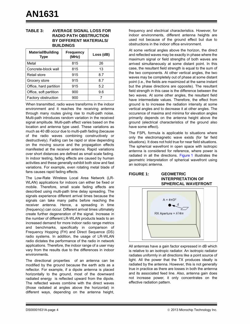
The FSPL formula is applicable to situations where only the electromagnetic wave exists (for far field situations). It does not hold true for near field situations. The spherical wavefront in open space with isotropic antenna is considered for reference, where power is radiated in all the directions. Figure 1 illustrates the geometric interpretation of spherical wavefront using an isotropic antenna.
FIGURE 1: GEOMETRIC INTERPRETATION OF SPHERICAL WAVEFRONT
All antennas have a gain factor expressed in dB which is relative to an isotropic radiator. An isotropic radiator radiates uniformly in all directions like a point source of light. All the power that the TX produces ideally is radiated by the antenna. However, this is not generally true in practice as there are losses in both the antenna and its associated feed line. Also, antenna gain does not increase power, it only concentrates on the effective radiation pattern.
DS00001631A-page 4 2013 Microchip Technology Inc.
AN1631
RANGE AND PERFORMANCE MEASUREMENTS OF SUB-GHZ MODULES
Performance Measurement Parameters
The following are some general concerns in communication systems:
• The radio distance acceptable between the TX and RX for communication
• The parameter changes required to enhance the range and gain for optimum performance
To resolve the above concerns, FSPL model is used in determining the transceiver separation, and changing (increase) the TX power to increase the separation distance. While these two assumptions work under restricted conditions, in general they are very useful for most situations. Apart from these two changes related to link budget, some emphasis on the data rate and protocol which cannot be undermined must be provided as these parameters are related to the frequency and modulation technique which are dependent on the operational band.
It is possible to improve the receive sensitivity and range by reducing data rates over air. Receive sensitivity is a function of the transmission baud rate. Receive sensitivity goes up as baud rate goes down. To maximize the range, many radios provide the user the ability to reduce the baud rate through its register configurations. Moreover, a better understanding of thewireless changes that needs to be done in the system can improve the transmission distance. In this application note, the measured field and data is presented that approximately supports the realistic math models.
This section provides details on various test factors that measure the performance of Microchip SUB-GHz radio modules.
The following are the test factors:
• Transmitting power
• Receive power
• Path loss and sensitivity performance
• PER/BER
• Range environment models
• Radiation pattern
• Impedance measurements
• Received Signal Strength Indicator (RSSI)
However, the following performance parameters including the range are measured in this application note:
• Range
• PER/BER
• Sensitivity Performance
• RSSI
Measurement Test Requirements and Setup
For measurements to be done, related hardware and software/utility setup are necessary. This section provides details of the hardware test setup and software/utilities used.
The Microchip MRF89XA modules and MRF49XA Sub-GHz transceiver based PICtail boards are used for the performance measurements. The MRF89XA Sub-GHz modules are FCC/ETSI/IC certified. These modules differ from other embedded Sub-GHz modules by offering a variety of regulatory and modularly certified Printed Circuit Board (PCB) antenna (Serpentine type) features. The MRF49XA Sub-GHz PICtail boards are based on wire type (/4) antenna for different frequencies, usually mounted on the development boards or daughter cards. For more information on the Sub-GHz modules, refer to Appendix A: “Microchip MRF89XA and MRF49XA PICtail boards Used for Measurements”.
HARDWARE USED FOR TEST SETUP
The following hardware are used for the range and performance parameter tests with the Sub-GHz transceiver modules:
• Two MRF89XAM8A/MRF89XAM9A/MRF49XA-433 MHz/MRF49XA-868 MHz/MRF49XA-915 MHz PICtail™/PICtail Plus Daughter Boards
• /4 length wire antennas for MRF49XA-433 MHz (~17.5 cm) and MRF49XA-868 / 915 MHz (~8.0 cm)
• Any of the following Microchip hardware development platforms:
- Two Explorer 16 Development Boards
(Part number: DM240001)
- Two PIC 18 Explorer Development Boards
(Part number: DM183032)
- Two 8-bit Wireless Development Boards
(Part number: DM182015)
- Any two custom developed boards which has the provision to mount the MRF89XA mod-ules/MRF49XA related PICtail boards
• One of the following Microchip development tools for programming/debugging:
- MPLAB® REAL ICE™ In-Circuit Emulator/MPLAB® ICD/PICkit™ 3
- ZENA™ Wireless Adapter: 868 MHz MRF89XA (AC182015-2) and 915 MHz MRF89XA (AC182015-3)
• Power supply: 9V/0.75A or equivalent battery pack
2013 Microchip Technology Inc. DS00001631A-page 5
AN1631
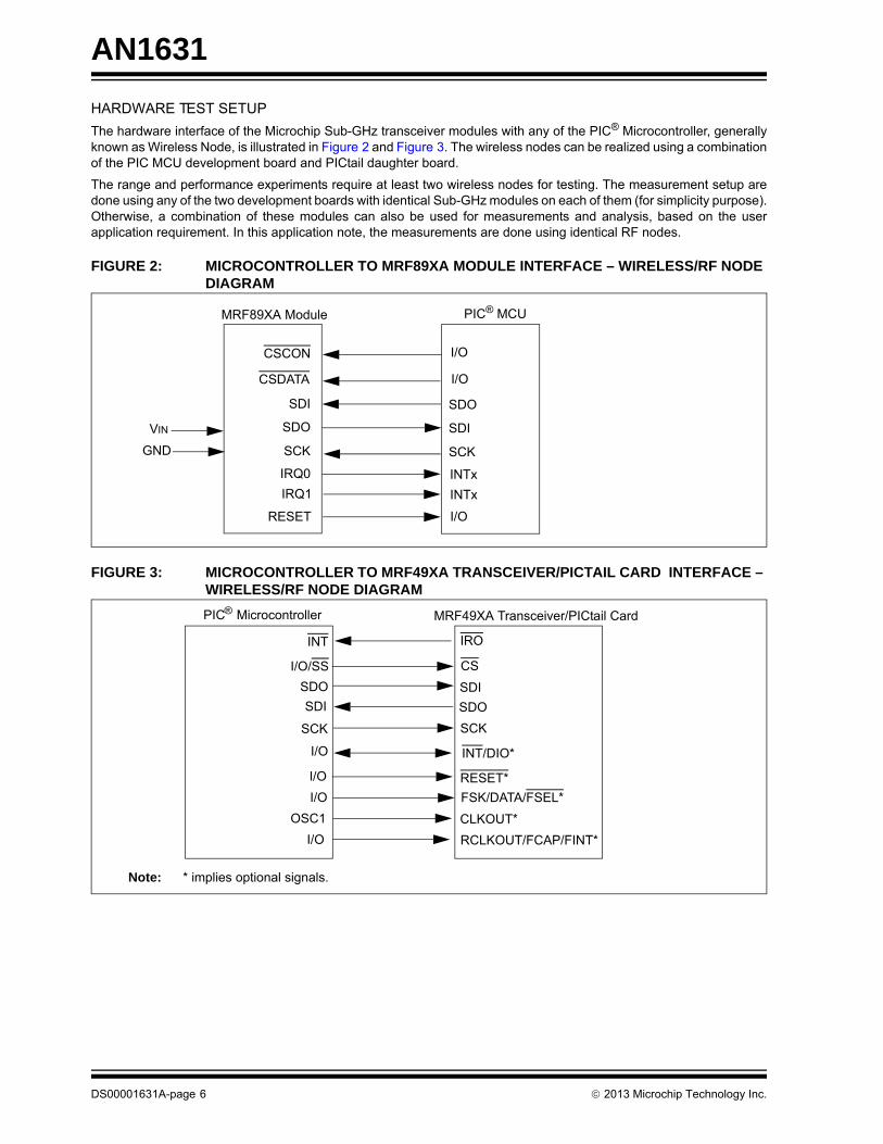
HARDWARE TEST SETUP
The hardware interface of the Microchip Sub-GHz transceiver modules with any of the PIC® Microcontroller, generally known as Wireless Node, is illustrated in Figure 2 and Figure 3. The wireless nodes can be realized using a combination of the PIC MCU development board and PICtail daughter board.
The range and performance experiments require at least two wireless nodes for testing. The measurement setup are done using any of the two development boards with identical Sub-GHz modules on each of them (for simplicity purpose). Otherwise, a combination of these modules can also be used for measurements and analysis, based on the user application requirement. In this application note, the measurements are done using identical RF nodes.
FIGURE 2: MICROCONTROLLER TO MRF89XA MODULE INTERFACE – WIRELESS/RF NODE DIAGRAM
CSDATA
CSCON
SDI
SDO
SCK
PIC® MCU
I/O
SDO
SDI
SCK
IRQ0 INTx
MRF89XA Module
RESET
VIN
GND
I/O
IRQ1 INTx
I/O
FIGURE 3: MICROCONTROLLER TO MRF49XA TRANSCEIVER/PICTAIL CARD INTERFACE – WIRELESS/RF NODE DIAGRAM
I/O/SS
SDI
SCK
I/O
MRF49XA Transceiver/PICtail Card
SDO
SCK
INT/DIO*
I/O
PIC® Microcontroller
I/O
RESET*
OSC1
I/O
SDO SDI
RCLKOUT/FCAP/FINT*
CLKOUT*
CS
FSK/DATA/FSEL*
INT IRO
Note: * implies optional signals.
DS00001631A-page 6 2013 Microchip Technology Inc.
AN1631
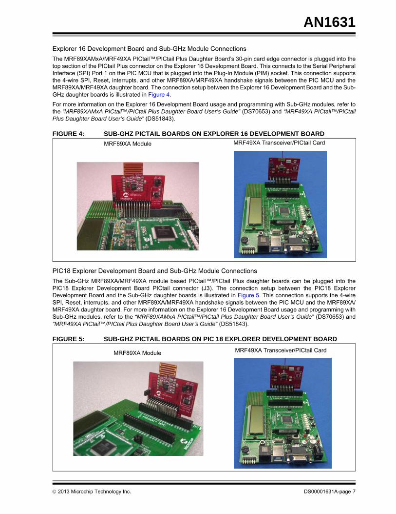
Explorer 16 Development Board and Sub-GHz Module Connections
The MRF89XAMxA/MRF49XA PICtail™/PICtail Plus Daughter Board’s 30-pin card edge connector is plugged into the top section of the PICtail Plus connector on the Explorer 16 Development Board. This connects to the Serial Peripheral Interface (SPI) Port 1 on the PIC MCU that is plugged into the Plug-In Module (PIM) socket. This connection supports the 4-wire SPI, Reset, interrupts, and other MRF89XA/MRF49XA handshake signals between the PIC MCU and the MRF89XA/MRF49XA daughter board. The connection setup between the Explorer 16 Development Board and the Sub-GHz daughter boards is illustrated in Figure 4.
For more information on the Explorer 16 Development Board usage and programming with Sub-GHz modules, refer to the “MRF89XAMxA PICtail™/PICtail Plus Daughter Board User’s Guide” (DS70653) and “MRF49XA PICtail™/PICtail Plus Daughter Board User’s Guide” (DS51843).
FIGURE 4: SUB-GHZ PICTAIL BOARDS ON EXPLORER 16 DEVELOPMENT BOARD
MRF89XA Module MRF49XA Transceiver/PICtail Card
PIC18 Explorer Development Board and Sub-GHz Module Connections
The Sub-GHz MRF89XA/MRF49XA module based PICtail™/PICtail Plus daughter boards can be plugged into the PIC18 Explorer Development Board PICtail connector (J3). The connection setup between the PIC18 Explorer Development Board and the Sub-GHz daughter boards is illustrated in Figure 5. This connection supports the 4-wire SPI, Reset, interrupts, and other MRF89XA/MRF49XA handshake signals between the PIC MCU and the MRF89XA/MRF49XA daughter board. For more information on the Explorer 16 Development Board usage and programming with Sub-GHz modules, refer to the “MRF89XAMxA PICtail™/PICtail Plus Daughter Board User’s Guide” (DS70653) and “MRF49XA PICtail™/PICtail Plus Daughter Board User’s Guide” (DS51843).
FIGURE 5:
MRF89XA Module MRF49XA Transceiver/PICtail Card
SUB-GHZ PICTAIL BOARDS ON PIC 18 EXPLORER DEVELOPMENT BOARD
2013 Microchip Technology Inc. DS00001631A-page 7
AN1631
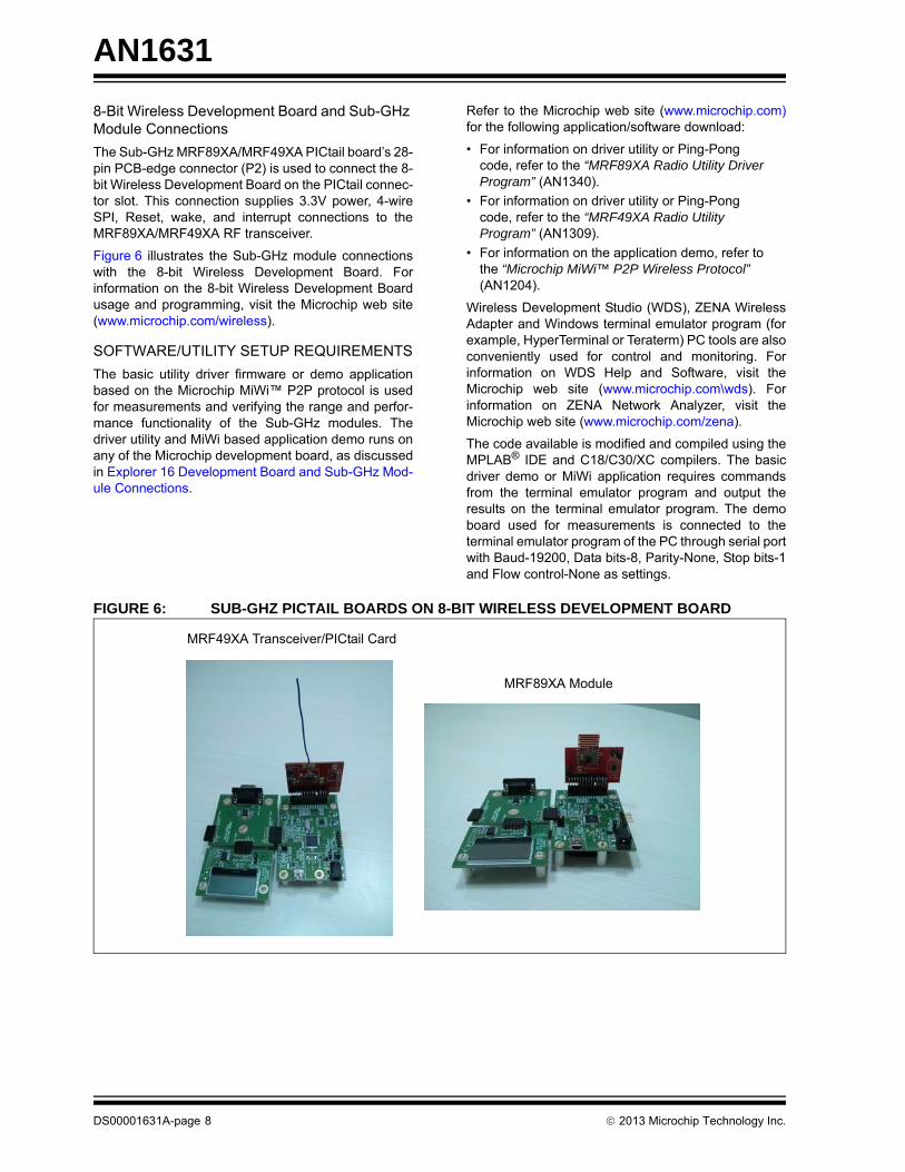
8-Bit Wireless Development Board and Sub-GHz Module Connections
The Sub-GHz MRF89XA/MRF49XA PICtail board’s 28-pin PCB-edge connector (P2) is used to connect the 8-bit Wireless Development Board on the PICtail connec-tor slot. This connection supplies 3.3V power, 4-wire SPI, Reset, wake, and interrupt connections to the MRF89XA/MRF49XA RF transceiver.
Figure 6 illustrates the Sub-GHz module connections with the 8-bit Wireless Development Board. For information on the 8-bit Wireless Development Board usage and programming, visit the Microchip web site (www.microchip.com/wireless).
SOFTWARE/UTILITY SETUP REQUIREMENTS
The basic utility driver firmware or demo application based on the Microchip MiWi™ P2P protocol is used for measurements and verifying the range and perfor-mance functionality of the Sub-GHz modules. The driver utility and MiWi based application demo runs on any of the Microchip development board, as discussed in Explorer 16 Development Board and Sub-GHz Mod-ule Connections.
Refer to the Microchip web site (www.microchip.com) for the following application/software download:
• For information on driver utility or Ping-Pong code, refer to the “MRF89XA Radio Utility Driver Program” (AN1340).
• For information on driver utility or Ping-Pong code, refer to the “MRF49XA Radio Utility Program” (AN1309).
• For information on the application demo, refer to the “Microchip MiWi™ P2P Wireless Protocol” (AN1204).
Wireless Development Studio (WDS), ZENA Wireless Adapter and Windows terminal emulator program (for example, HyperTerminal or Teraterm) PC tools are also conveniently used for control and monitoring. For information on WDS Help and Software, visit the Microchip web site (www.microchip.com\wds). For information on ZENA Network Analyzer, visit the Microchip web site (www.microchip.com/zena).
The code available is modified and compiled using the MPLAB® IDE and C18/C30/XC compilers. The basic driver demo or MiWi application requires commands from the terminal emulator program and output the results on the terminal emulator program. The demo board used for measurements is connected to the terminal emulator program of the PC through serial port with Baud-19200, Data bits-8, Parity-None, Stop bits-1 and Flow control-None as settings.
FIGURE 6: SUB-GHZ PICTAIL BOARDS ON 8-BIT WIRELESS DEVELOPMENT BOARD
MRF49XA Transceiver/PICtail Card
MRF89XA Module
DS00001631A-page 8 2013 Microchip Technology Inc.
AN1631
Summary of Tools Used for Range/Performance Measurements
The following must be ensured during indoor and outdoor tests/measurements:
• Explorer 16 Development Boards/PIC18 Development Boards/8-bit Wireless Development Board are used with a provision for mounting and plugging the battery pack in the general purpose PCB area.
• Versions of the module boards have some variations in the RF power output.
• PCB antenna must be protruded outside the development board to minimize the interference and enhance the lobe power.
• MiWi P2P Simple Demo Code is used for testing with slight code modifications. However, Ping-Pong related code and MRF89XA or MRF49XA Driver Software are also used depending on the requirement.
• Configure for MRF49XA-866 MHz and MRF49XA-915 MHz is done through software while the hardware for both of these modules remain the same.
• Terminal emulator program on PC/ZENA Wireless Adapter/LCD can be used as display units. How-ever, for open field environment on-board LCD would consume less power from its battery source.
Table 4 provides a detailed list of the hardware and software tools used for measurements in this application note. As discussed in Explorer 16 Development Board and Sub-GHz Module Connections and Summary of Tools Used for Range/Performance Measurements, the test setup requires two sets of hardware for transmission and reception at any time, and the process is repeated vice-versa.
TABLE 4: TOOLS FOR RANGE/PERFORMANCE MEASUREMENTS
Mother Board/Base
Board
DaughterCard Name
with Module/Rev.
Daughter Card Part Number
DaughterCard Details
CardsUsed
Max. Power (dB)
AntennaType
AntennaDirection
Antenna Length
(cm)
Demonstration Program
Monitoring/Display
Explorer 16/PIC18 Explorer/8-bit Wireless Development Board
MRF89XAMxA(Rev. R1) PICtail/PICtail Plus Daughter Board
AC164138-1 MRF89XAM8A868 MHzRev. R1
2 +10 PCB Vertical NA MiWi P2P Simple Demo/Simple P2P Ping-Pong/MRF89XA DriverSoftware (PER, RSSI, and so on)
Terminal emulator program on PC/ZENA Wireless Adapter on PC/LCD
Explorer 16/PIC18 Explorer/8-bit Wireless Development Board
MRF89XAMxA(Rev. R1) PICtail/PICtail Plus Daughter Board
AC164138-2 MRF89XAM9A915 MHzRev. R1
2 +10 PCB Vertical NA MiWi P2P Simple Demo/Simple P2P Ping-Pong/MRF89XA DriverSoftware (PER, RSSI, and so on)
Terminal emulator program on PC/ZENA Wireless Adapter on PC/LCD
Explorer 16/PIC18 Explorer/8-bit Wireless Development Board
MRF49XA (Rev. R2) PICtail/PICtail Plus Daughter Board
AC164137-1 MRF49XA433 MHzRev. R2
2 + 7 Wire Vertical 17.5 MiWi P2P Simple Demo/Simple P2P Ping-Pong/MRF49XA Driver Software (PER, RSSI, and so on)
Terminal emulator program on PC/ZENA Wireless Adapter on PC/LCD
Explorer 16/PIC18 Explorer/8-bit Wireless Development Board
MRF49XA (Rev. R2) PICtail/PICtail Plus Daughter Board
AC164137-2 MRF49XA868 MHzRev. R2
2 + 7 Wire Vertical MiWi P2P Simple Demo/Simple P2P Ping-Pong/MRF49XA Driver Software (PER, RSSI, and so on)
Terminal emulator program on PC/ZENA Wireless Adapter on PC/LCD
Explorer 16/PIC18 Explorer/8-bit Wireless Development Board
MRF49XA (Rev. R2) PICtail/PICtail Plus Daughter Board
AC164137-2 MRF49XA915 MHzRev. R2
2 + 7 Wire Vertical MiWi P2P Simple Demo/Simple P2P Ping-Pong/MRF49XA Driver Software (PER, RSSI, and so on)
Terminal emulator program on PC/ZENA Wireless Adapter on PC/LCD
Note: Any of the custom application code (simple user application specific code) can also be used for measurements.
2013 Microchip Technology Inc. DS00001631A-page 9

AN1631
MEASUREMENT AND PERFORMANCE TEST
Range Measurement Environments
Operating terrains (environments) highly impact the wave propagation. Range tests are conducted in a variety of indoor and outdoor environments to provide a basic understanding of the range performance that the Sub-GHz modules are capable of. The chosen environments include Line of Sight (LOS) on level and uneven terrain, and obstructed paths on level and uneven terrain.
The measurements are also based on the following factors:
• PCB antenna orientation (vertical or horizontal)
• Output power of the Sub-GHz modules (maximum or default)
• Power Amplifier (PA)/Low Noise Amplifier (LNA) (enabled or disabled value)
• Type of antenna PCB/Wire/Standard dipole
• Antenna (Serpentine, wire or whip/dipole)
The factors affecting indoor measurements:
• Office equipments
- Wi-Fi/Bluetooth/Microwave in the vicinity
- Concrete structures/walls/glass nearby/wood/metal, and so on
The purpose of actual measurements for outdoor and indoor, and understanding the operating scenes is to gain confidence in the operating environment. Ideally, the wireless networks commissioned are not be operated in a conducive environment.
Typical environments that are considered in this application note for range testing are as follows:
• Outdoor: Open plane field (with even surface)
• Outdoor: Open plane field (with irregular surface)
• Outdoor: Vicinity of buildings
• Indoor: Office/home environment
• Indoor: Inter floor test (indoor)
• Indoor/Outdoor: PER test in open plane field and office environment
For range tests, the main differentiating factors are the module mounting, antenna orientation and the constant battery power source (not allowing the source voltage to drop below supply voltage requirements).
Figure 7 illustrates the vertical (with elevation lobe/plane) and horizontal (with azimuth lobe/plane) mounting of antenna on the base board. The antenna is mounted either vertically or horizontally based on the effective output power achieved, application space requirements and constraints (i.e., having a strong primary lobe based on the center fundamental frequency and secondary lobes based on its third harmonic frequency). As radio frequencies are reduced, the antenna sizes increase proportionally and the calculations in Equation 3 show the antenna wire sizes for Sub-GHz antennas.
EQUATION 3: ANTENNA WIRE SIZE
WireLength cm 7500Frequency Hz ----------------------------------------=
For,
433 MHz ~ 17.3 cm
915 MHz ~ 8.2 cm
Note: This equation holds good for antenna wire size = 1/4 wavelength.
FIGURE 7:
433 MHz
868 MHz/915 MHz
868 MHz/915 MHz (With PCB Antenna)
MRF49XA AND MRF89XA PICTAIL BOARDS – VERTICAL MOUNTING
DS00001631A-page 10 2013 Microchip Technology Inc.
AN1631
Range Measurement ProcedureThe following is the procedure on how to conduct simple range test or measurements:
1. Program the two RF/wireless Sub-GHz based transceiver nodes with MiWi P2P demo code.
2. Place any one RF node on a stand (5 ft.-6 ft.pole) as illustrated in Figure 8 after configuring a specific operating channel. By default, the wireless node is in receiving mode.
3. Place a similar RF node on a second stand (5 ft.-6 ft. pole) and set for the same working channel.
4. Make one of the nodes stationary and the other node mobile.
5. Setup nodes and ensure the two nodes are connected to each other.
6. Move the mobile node and test for transmission and reception. Measure for every 5 ft.-10 ft.
7. Once the critical point is attained, measure the actual/radial distance from the TX to the RX.
Note: Critical distance is a point where the TX and RX communication becomes intermittent.
8. Return 5 ft. from the critical point and check for reliable communication.
On a conservative note, subtract 5 ft.-10 ft. from the critical distance to get the actual range.
Note: Range is the least radius or linear radio distance measured between two antennas.
Figure 8 illustrates the ideal test setup for any lab mea-surements including the mounting and arrangement. However, the field test setup does not involve any com-plexities such as anechoic chamber or ideal LOS envi-ronments.
FIGURE 8: SUB-GHZ MODULE/RF NODE-LAB MOUNTING
2013 Microchip Technology Inc. DS00001631A-page 11
AN1631
Figure 9 illustrates the distance measurement method, and it also shows that the increase in range value is a function of variables with the TX module height being most sensitive.
FIGURE 9:
Stationary Antenna (Module A)
Ground Level Mobile Antenna (Module B)
Antenna Height
Range/Distance (d) in Meters
Direction of Travel
DISTANCE MEASUREMENT METHOD
Figure 10 illustrates the outdoor measurement test setup for open field/PER/BER test.
FIGURE 10:
Range/Radio Distance
OUTDOOR MEASUREMENTS TEST SETUP: OPEN FIELD/PER/BER TEST
Figure 11 illustrates the outdoor measurement test setup for vicinity of buildings.
FIGURE 11:
Range/Radio Distance
OUTDOOR MEASUREMENTS TEST SETUP: VICINITY OF BUILDINGS
DS00001631A-page 12 2013 Microchip Technology Inc.
AN1631
Figure 12 illustrates the outdoor measurement test setup for buildings in between antennas.
FIGURE 12: OUTDOOR MEASUREMENTS TEST SETUP: BUILDINGS IN BETWEEN ANTENNAS
Range/Radio Distance
Figure 13 illustrates the indoor measurement test setup for office/PER/BER test.
FIGURE 13: INDOOR MEASUREMENTS TEST SETUP
Range/Radio Distance
: OFFICE/PER/BER TEST
Figure 14 illustrates the indoor measurement test setup for inter floor.
FIGURE 14:
Antenna A
Antenna B
INDOOR MEASUREMENTS TEST SETUP: INTER FLOOR
2013 Microchip Technology Inc. DS00001631A-page 13

AN1631
MEASUREMENT ENVIRONMENT AND RESULTS
This section provides different type of environmentsand conditions used for performing range tests. The basic idea adopted is to conduct outdoor (nearly LOS) and indoor tests (with obstacles), to measure the nature and characteristics that each of the modules contribute for performance in different environments.
The following different types of environments (indicated in abbreviations) are considered for range/other perfor-mance measurements:
• Outdoor measurement setup
- Open field: Even surface (OP(E))
- Open field: Uneven surface (OP(U))
- Vicinity of buildings: Even surface (VOB(E))
- Vicinity of buildings: Uneven surface (VOB(U))
- Building/s in-between TX and RX antenna: Even surface (BIA(E))
• Indoor measurement setup
- Indoor: Office
Outdoor Measurement Environments
ENVIRONMENT: OPEN FIELD
• Test: Range/PER/BER
• Land characteristics: Even
• Reference level: Ground
• Mounting: 5 ft. above ground
• Antenna orientation: Vertical
• Operating frequency: 433 MHz, 868 MHz, and 915 MHz
• Operating channels: 0-10
Figure 15 illustrates the outdoor measurement done in an open field with even surface.
FIGURE 15: OPEN FIELD - EVEN SURFACE
ENVIRONMENT: OPEN FIELD
• Test: Range
• Land characteristics: Uneven
• Reference level: Ground
• Mounting: 5 ft. above ground
• Antenna orientation: Vertical
• Operating frequency: 433 MHz, 868 MHz, and 915 MHz
• Operating channels: 0-10
Figure 16 illustrates the outdoor measurement done in an open field with uneven surface.
FIGURE 16: OPEN FIELD - UNEVEN SURFACE
ENVIRONMENT: VICINITY OF BUILDINGS
• Test: Range
• Land characteristics: Even/Uneven
• Reference level: Ground
• Mounting: 5 ft. above ground
• Antenna orientation: Vertical
• Operating frequency: 433 MHz, 868 MHz, and 915 MHz
• Operating channels: 0-10
Figure 17 illustrates the outdoor measurement done near vicinity of buildings.
FIGURE 17: OUTDOOR: VICINITY OF BUILDINGS
DS00001631A-page 14 2013 Microchip Technology Inc.
AN1631
ENVIRONMENT: BUILDING IN BETWEEN
• Test: Range
• Land characteristics: Even/uneven
• Reference level: Ground
• Mounting: 5 ft. above ground
• Antenna orientation: Vertical
• Operating frequency: 433 MHz, 868 MHz, and 915 MHz
• Operating channel: 0-10
Figure 18 illustrates the outdoor measurement done in between buildings.
FIGURE 18: OUTDOOR: BUILDINGS IN BETWEEN
Indoor Measurement Environments
ENVIRONMENT: OFFICE
• Test: Range/PER/BER
• Land characteristics: Level
• Reference level: Same floor
• Mounting: 5 ft. above ground, cubical top
• Antenna orientation: Vertical
• Operating frequency: 433 MHz, 868 MHz, and 915 MHz
• Operating channel: 0-10
Figure 19 illustrates the indoor measurements done inside office (same floor).
FIGURE 19: INDOOR: OFFICE
ENVIRONMENT: OFFICE
• Test: Range
• Land characteristics: Level
• Reference level: Inter floor
• Mounting: 3 ft. above ground, on table
• Antenna orientation: Vertical
• Operating frequency: 433 MHz, 868 MHz, and 915 MHz
• Operating channel: 0-10
• Inter floor distance: 13 ft.
Figure 20 illustrates the indoor measurement done in the office (inter floor).
FIGURE 20: INDOOR: OFFICE (INTER FLOOR)
2013 Microchip Technology Inc. DS00001631A-page 15
AN1631
Range Measurement Conditions and Results
The IEEE 802.15.4 physical layer offers a total of 27 channels where, one channel is in the 868 MHz band, ten channels are in the 915 MHz band, and 16 channels are in the 2.4 GHz band. The raw bit rates on these three frequency bands are 20 kbps, 40 kbps, and 250 kbps, respectively. In theory, all Sub-GHz bands can be segregated by logical or custom channels which include the 433 MHz band which would have a lesser throughput. The frequency deviation decides the differentiation in channels or channel spacing which are dependent on the specific transceiver modulation support.
MRF49XA modulates signal using Frequency Shift Keying (FSK) with appropriate frequency deviation for channel spacing. For more information, refer to the “MRF49XA Data Sheet” (DS70590). The user can choose to operate at one of the frequency bands: 433 MHz, 868 MHz or 915 MHz, and then proceed to program the center frequency. The frequency deviation can be set to 15 kHz, 30 kHz, 45 kHz, 90 kHz or 120 kHz. Frequency deviations for MRF49XA can be set in steps of 15 kHz up to 240 kHz.
Similarly, MRF89XA supports FSK and On-Off Keying (OOK) with appropriate frequency deviation for chan-nel spacing. For more information, refer to the “MRF89XA Data Sheet” (DS70622). The user can operate at one of the frequency bands: 902 MHz-915 MHz, 915 MHz-928 MHz, 950 MHz-960 MHz or 863 MHz-870 MHz, and then proceed to program the center frequency. The frequency deviation can be set as 200 kHz, 133 kHz, 100 kHz, 80 kHz, 67 kHz, 50 kHz, 40 kHz, and 33 kHz. The default value for frequency deviation is the value selected during the transceiver setup procedure.
The following settings must be ensured to accomplish the range measurements:
• Less noisy Sub-GHz channel is assigned as the operating channel for all the measurements.
• Transmit power is controlled by the TXCONREG register for MRF89XA and TXCREG register for MRF49XA and is assigned as default. Refer to the specific device/module data sheet for more information on the settings.
• Data rate is set as required (standard/default)
• Baud rate is set as 19200 for communication between terminal emulator and node’s serial port is used for monitoring and debug purpose.
Table 5 provides the measured range details of the Sub-GHz modules. The environment and other conditions are also specified in this table.
The range measurement test conditions for MRF89XA transceiver modules are as follows:
• Transceivers: MRF89XA
• Environment: Specified in Table 5
• Land characteristics: Specified in Table 5
• Level: Ground
• Antenna orientation: Vertical
• Operating frequency: 863 MHz, 902 MHz, 915 MHz, and 950 MHz
• Operating channels: 0-10
• Date rate: 20/40 kbps
• Data packets transmitted: Variable string packet
• LNA GAIN: 0/10 dB
• TX Power: 0 dB
• RSSI Threshold: -79 dB
The range measurement test conditions for MRF49XA transceiver modules are as follows:
• Transceivers: MRF49XA
• Environment: Specified in Table 5
• Land characteristics: Specified in Table 5
• Level: Ground
• Antenna orientation: Vertical
• Operating frequency: 43 MHz/434 MHz, 868 MHz, and 915 MHz
• Operating channels: 0-10
• Date rate: 20/40 kbps
• Data packets transmitted: Variable string packet
• LNA GAIN: 0/7 dB
• TX Power: 0 dB
• RSSI Threshold: -79 dB
Apart from above test above conditions, the radiated power from each module can be estimated to the sum of TX power present at antenna feeding point and average antenna gain.
On average, the radiated power estimations are as follows:
• MRF89XAM8A (868 MHz):
-0.5 dBm + 1.5 dB + 0 dBm = 1 dBm
-0.5 dBm + 1.5 dB + 10 dBm = 11 dBm
• MRF89XAM9A (915 MHz):
-0.5 dBm + 1.5 dB + 0 dBm = 1 dBm
-0.5 dBm + 1.5 dB + 10 dBm = 11 dBm
• MRF49XA-433 MHz: -0.5 dBm + 1.5 dB = 1 dBm
• MRF49XA-868 MHz: -0.5 dBm + 1.5 dB = 1 dBm
• MRF49XA-915 MHz: -0.5 dBm + 1.5 dB = 1 dBm
DS00001631A-page 16 2013 Microchip Technology Inc.
AN1631
TABLE 5: RANGE MEASUREMENT RESULTS OF SUB-GHZ MODULES
Module Type
Antenna Type and
Position
Frequency (MHz)
Power Setting
(dB)Environment/View Terrain
Range (in Meters)With ACK
Range (in Meters)
Without ACK
Inter-Floor Communication
MRF89XAM8A PCB 868 10 Office — 60-70 70-80 Office environment, four floors
Outside office — 85-95 110-115
Vicinity of buildings — 95-105 115-120
Open field Uneven surface 320-330 340-350
Open field Even surface 700-725 725-750
MRF89XAM9A PCB 915 10 Office — 50-60 60-70 Office environment, three floors
Outside office — 75-80 95-105
Vicinity of buildings — 85-95 110-115
Open field Uneven surface 280-290 300-310
Open field Even surface 650-675 675-700
MRF89XAM8A PCB 868 0 Office — 45-50 50-55 Office environment, two floors
Outside office — 80-85 110-115
Vicinity of buildings — 90-95 115-120
Open field Uneven surface 250-260 270-280
Open field Even surface 340-350 360-370
MRF89XAM9A PCB 915 0 Office — 40-45 45-50 Office environment, two floors
Outside office — 75-80 100-105
Vicinity of buildings — 80-85 110-115
Open field Uneven surface 220-230 240-250
Open field Even surface 320-330 330-350
MRF49XA Wire 433 0 Office — 60-70 70-80 Office environment, two floors
Outside office — 90-95 120-125
Vicinity of buildings — 100-105 125-130
Open field Uneven surface 290-300 310-320
Open field Even surface 350-360 380-390
MRF49XA Wire 868 0 Office — 45-50 50-55 Office environment, two floors
Outside office — 80-85 110-115
Vicinity of buildings
— 90-95 115-120
Open field Uneven surface 250-260 270-280
Open field Even surface 340-350 360-370
MRF49XA Wire 915 0 Office — 40-45 45-50 Office environment, two floors
Outside office — 75-80 100-105
Vicinity of buildings
— 80-85 110-115
Open field Uneven surface 220-230 240-250
Open field Even surface 320-330 340-350
Note 1: All the range measurement results specified in Table 5 are conservative and may vary based on the environment and test conditions. However, better results may be achieved by further refining the tests conducted.
2: For more information on variable power configuration, refer to the device “MRF89XA Data Sheet” (DS70622) and “MRF49XA Data Sheet” (DS70590), and related MRF89XA and MRF49XA module/PICtail board data sheet.
3: The frequency band, center frequency, bandwidth and the data rate values on both transceivers (sender and receiver units) must be the same for successful reception of the transmitted content.
4: The power measurements are not part of the table as to suppress the ambiguity of environment variables.
2013 Microchip Technology Inc. DS00001631A-page 17
AN1631
Packet Error Rate (PER) Test
PER TEST BETWEEN TWO DEVICES
The PER test analyses the indoor and outdoor valid data coverage between two wireless nodes. This section explains a simple PER test setup and its procedure. The PER test setup is similar to the open field test setup.
The PER test between two devices is done in a single iteration with predetermined number of data packets. The ISM/IEEE 802.15.4 specification defines a reliable link as having PER below or equal to 1% for the 1000 data packets transmitted/received. PER measures the capability of a device to receive a signal without degradation due to undesirable signals at other frequencies. The desired signal’s degradation of its PER must be less than 1% or the BER must be less than 0.1%. PER test is conducted by adding the delay between data packets, if required. For more information, refer to the “MRF89XA Radio Utility Driver Program” (AN1340) and “MRF49XA Radio Utility Program” (AN1309).
The following is the procedure to conduct simple PER test measurements:
1. Program the two Sub-GHz based transceiver wireless nodes with Utility Driver firmware for PER test.
2. Place any one RF node on a stand (5 ft.-6 ft. pole) as illustrated in Figure after configuring a specific operating channel. By default, the wireless node is in receiving mode.
3. Place a similar RF node on a second stand (5 ft.-6 ft. pole) and set for the same working channel.
4. Make one of the nodes stationary and the other node mobile.
5. Setup nodes and ensure the two nodes are connected to each other.
6. Trigger the following sequence for the secondRF node, as illustrated in Figure 21.
7. The RF node sends a message/request to the first module to start sending 100/1000 datapackets, and immediately the RF node enters Receive mode to handle all of these 100/1000 incoming data packets.
8. Move the mobile node and test for transmission and reception for every 5 ft.-10 ft., and record the reading.
FIGURE 21: TRANSMITTER-RECEIVER SCREENS DURING PER TEST
DS00001631A-page 18 2013 Microchip Technology Inc.
2013
Microchip T
echnology Inc.D
S0
0001631A-p
age 19
AN
1631
PE
Ad itions specified in Outdoor MeasurementEn or environment. The table cells show the nu
TA
300 (m)
500 (m)
750 (m)
1000 (m)
1500 (m)
M 1000 1000 980 0 0
M 1000 1000 950 0 0
M 990 0 0 0 0
M 975 0 0 0 0
M 995 0 0 0 0
M 985 0 0 0 0
M 975 0 0 0 0
Ta ts received for every 1000 data packets tra
TA
300 (m)
500 (m)
750 (m)
1000 (m)
1500 (m)
M 0 0 0 0 0
M 0 0 0 0 0
M 0 0 0 0 0
M 0 0 0 0 0
M 0 0 0 0 0
M 0 0 0 0 0
M 0 0 0 0 0
R TEST CONDITIONS AND RESULTS
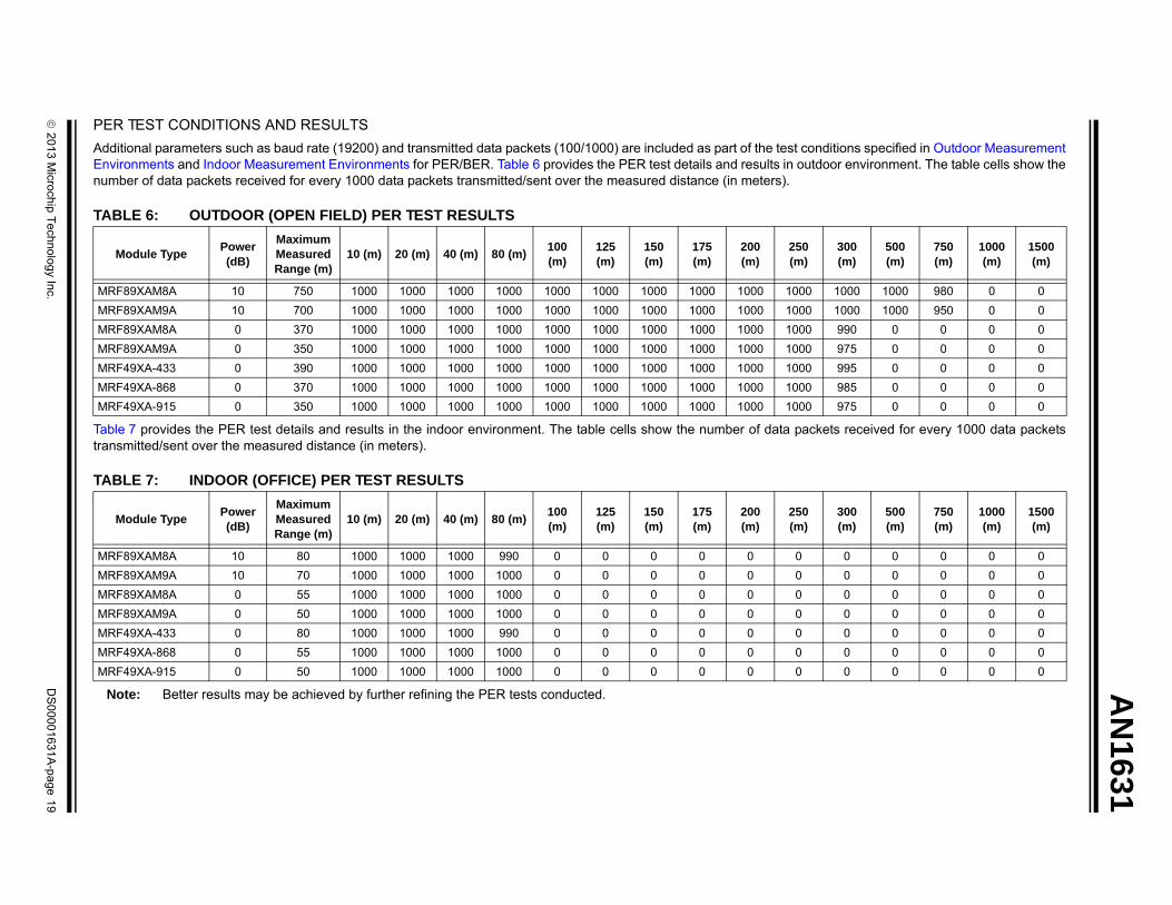
ditional parameters such as baud rate (19200) and transmitted data packets (100/1000) are included as part of the test condvironments and Indoor Measurement Environments for PER/BER. Table 6 provides the PER test details and results in outdomber of data packets received for every 1000 data packets transmitted/sent over the measured distance (in meters).
BLE 6:
Module TypePower (dB)
Maximum Measured Range (m)
10 (m) 20 (m) 40 (m) 80 (m)100 (m)
125 (m)
150 (m)
175 (m)
200 (m)
250 (m)
RF89XAM8A 10 750 1000 1000 1000 1000 1000 1000 1000 1000 1000 1000
RF89XAM9A 10 700 1000 1000 1000 1000 1000 1000 1000 1000 1000 1000
RF89XAM8A 0 370 1000 1000 1000 1000 1000 1000 1000 1000 1000 1000
RF89XAM9A 0 350 1000 1000 1000 1000 1000 1000 1000 1000 1000 1000
RF49XA-433 0 390 1000 1000 1000 1000 1000 1000 1000 1000 1000 1000
RF49XA-868 0 370 1000 1000 1000 1000 1000 1000 1000 1000 1000 1000
RF49XA-915 0 350 1000 1000 1000 1000 1000 1000 1000 1000 1000 1000
OUTDOOR (OPEN FIELD) PER TEST RESULTS
ble 7 provides the PER test details and results in the indoor environment. The table cells show the number of data packensmitted/sent over the measured distance (in meters).
BLE 7: INDOOR (OFFICE) PER TEST RESULTS
Module TypePower (dB)
Maximum Measured Range (m)
10 (m) 20 (m) 40 (m) 80 (m)100 (m)
125 (m)
150 (m)
175 (m)
200 (m)
250 (m)
RF89XAM8A 10 80 1000 1000 1000 990 0 0 0 0 0 0
RF89XAM9A 10 70 1000 1000 1000 1000 0 0 0 0 0 0
RF89XAM8A 0 55 1000 1000 1000 1000 0 0 0 0 0 0
RF89XAM9A 0 50 1000 1000 1000 1000 0 0 0 0 0 0
RF49XA-433 0 80 1000 1000 1000 990 0 0 0 0 0 0
RF49XA-868 0 55 1000 1000 1000 1000 0 0 0 0 0 0
RF49XA-915 0 50 1000 1000 1000 1000 0 0 0 0 0 0
Note: Better results may be achieved by further refining the PER tests conducted.
AN
1631
DS
00001631A
-page 20
2013 M
icrochip Technolo
gy Inc.
hods exist that enables for direct BER le method is to calculate BER from PER. The
R/BER is similar to the range measurement.
RESULTS
ud rate (19200) and transmitted data packets of the test conditions specified in Outdoor Indoor Measurement Environments for PER/est details and results in outdoor environment st details and results in indoor environemnt. of data packets received for every 1000 data measured distance (in meters).
0 )
300 (m)
500 (m)
750 (m)
1000 (m)
1500 (m)
0 1000 1000 980 0 0
0 1000 1000 950 0 0
0 990 0 0 0 0
0 975 0 0 0 0
0 995 0 0 0 0
0 985 0 0 0 0
0 975 0 0 0 0
0 )
300 (m)
500 (m)
750 (m)
1000 (m)
1500 (m)
0 0 0 0 0
0 0 0 0 0
0 0 0 0 0
0 0 0 0 0
0 0 0 0 0
0 0 0 0 0
0 0 0 0 0
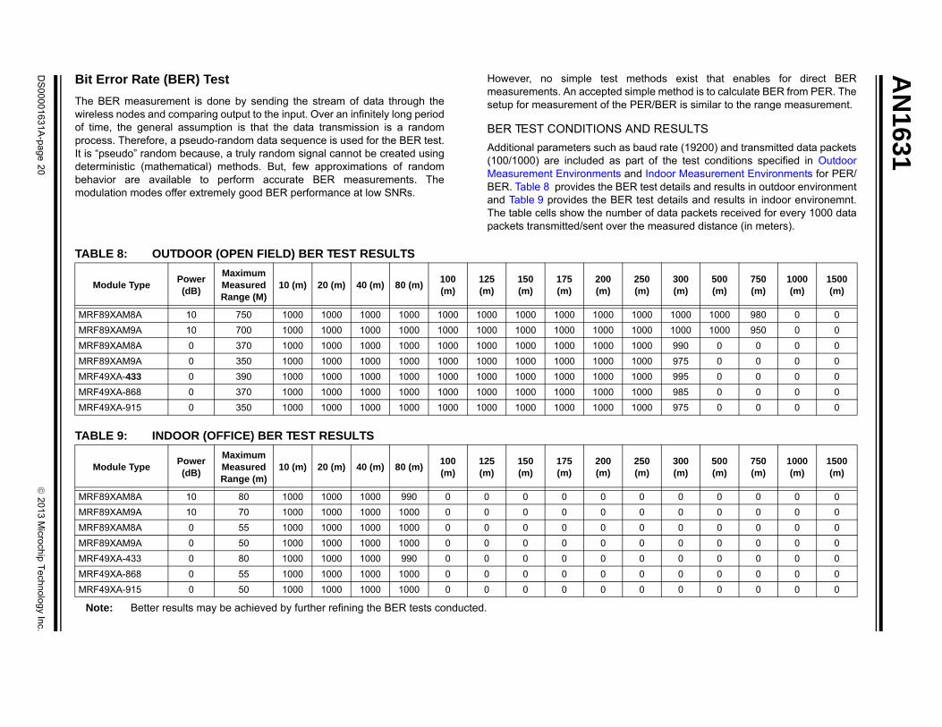
Bit Error Rate (BER) Test
The BER measurement is done by sending the stream of data through the wireless nodes and comparing output to the input. Over an infinitely long period of time, the general assumption is that the data transmission is a random process. Therefore, a pseudo-random data sequence is used for the BER test. It is “pseudo” random because, a truly random signal cannot be created using deterministic (mathematical) methods. But, few approximations of random behavior are available to perform accurate BER measurements. The modulation modes offer extremely good BER performance at low SNRs.
However, no simple test metmeasurements. An accepted simpsetup for measurement of the PE
BER TEST CONDITIONS AND
Additional parameters such as ba(100/1000) are included as partMeasurement Environments and BER. Table 8 provides the BER tand Table 9 provides the BER teThe table cells show the number packets transmitted/sent over the
TABLE 8: OUTDOOR (OPEN FIELD) BER TEST RESULTS
Module TypePower (dB)
Maximum Measured Range (M)
10 (m) 20 (m) 40 (m) 80 (m)100 (m)
125 (m)
150 (m)
175 (m)
200 (m)
25(m
MRF89XAM8A 10 750 1000 1000 1000 1000 1000 1000 1000 1000 1000 100
MRF89XAM9A 10 700 1000 1000 1000 1000 1000 1000 1000 1000 1000 100
MRF89XAM8A 0 370 1000 1000 1000 1000 1000 1000 1000 1000 1000 100
MRF89XAM9A 0 350 1000 1000 1000 1000 1000 1000 1000 1000 1000 100
MRF49XA-433 0 390 1000 1000 1000 1000 1000 1000 1000 1000 1000 100
MRF49XA-868 0 370 1000 1000 1000 1000 1000 1000 1000 1000 1000 100
MRF49XA-915 0 350 1000 1000 1000 1000 1000 1000 1000 1000 1000 100
TABLE 9: INDOOR (OFFICE) BER TEST RESULTS
Module TypePower (dB)
Maximum Measured Range (m)
10 (m) 20 (m) 40 (m) 80 (m)100 (m)
125 (m)
150 (m)
175 (m)
200 (m)
25(m
MRF89XAM8A 10 80 1000 1000 1000 990 0 0 0 0 0 0
MRF89XAM9A 10 70 1000 1000 1000 1000 0 0 0 0 0 0
MRF89XAM8A 0 55 1000 1000 1000 1000 0 0 0 0 0 0
MRF89XAM9A 0 50 1000 1000 1000 1000 0 0 0 0 0 0
MRF49XA-433 0 80 1000 1000 1000 990 0 0 0 0 0 0
MRF49XA-868 0 55 1000 1000 1000 1000 0 0 0 0 0 0
MRF49XA-915 0 50 1000 1000 1000 1000 0 0 0 0 0 0
Note: Better results may be achieved by further refining the BER tests conducted.
AN1631
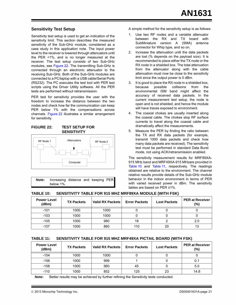
Sensitivity Test Setup
Sensitivity test setup is used to get an indication of the sensitivity limit. This section describes the measured sensitivity of the Sub-GHz module, considered as a case study in this application note. The input power level to the receiver is lowered through attenuators until the PER <1%, and is no longer measured at the receiver. The test setup consists of two Sub-GHz modules, see Figure 22. The transmitting Sub-GHz is connected through an electronic attenuator to the receiving Sub-GHz. Both of the Sub-GHz modules are connected to a PC/laptop with a USB cable/Serial Ports (RS232). The PC executes the test tool with PER test scripts using the Driver Utility software. All the PER tests are performed without retransmission.
PER test for sensitivity provides the user with the freedom to increase the distance between the two nodes and check how far the communication can keep PER below 1% with the compensations across channels. Figure 22 illustrates a similar arrangement for sensitivity.
FIGURE 22: TEST SETUP FOR SENSITIVITY
Computer
AttenuatorsRF Node 1 RF Node 2
Note: Increasing distance and keeping PER below 1%.
A simple method for the sensitivity setup is as follows:
1. Use two RF nodes and a variable attenuator between the RX and TX board with SubMiniature version A (SMA) antenna connector for Whip type, and so on.
2. Increase the attenuation until the data packets are lost (% depends on the payload size). It is recommended to place either the TX node or the RX node in a shielded box. The total attenuation from the attenuator along with the cable attenuation must now be close to the sensitivity limit since the output power is 0 dBm.
3. It is good to place the RX node in a shielded box, because possible collisions from the environmental ISM band might affect the accuracy of received data packets. In the current measurement test setup, the node is open and is not shielded, and hence the module will have traces exposed to environment.
4. The coaxial chokes are usually inserted along the coaxial cable. The chokes stop RF surface currents to travel along the coaxial cable and dramatically affect the measurements.
5. Measure the PER by finding the ratio between the TX and RX data packets (for example, transmit 1000 data packets and check how many data packets are received). The sensitivity test must be performed in standard Data Burst mode, not using ACK/retransmission enabled.
The sensitivity measurement results for MRF89XA-915 MHz band and MRF49XA-915 MHzare provided in Table 10 and Table 11, respectively. The readings obtained are relative to the environment. The channel relative results provide details of the Sub-GHz module behavior in the indoor environment in terms of PER with varied received power in dBm. The sensitivity tables are based on PER ≤1%.
TABLE 10: SENSITIVITY TABLE FOR 915 MHZ MRF89XA MODULE (WITH FSK)
Power Level (dBm)
TX Packets Valid RX Packets Error Packets Lost PacketsPER at Receiver
(%)
-101 1000 1000 0 0 0
-103 1000 1000 0 0 0
-105 1000 980 18 2 2.0
-107 1000 860 110 20 13
TABLE 11: SENSITIVITY TABLE FOR 915 MHZ MRF49XA PICTAIL BOARD (WITH FSK)
Power Level (dBm)
TX Packets Valid RX Packets Error Packets Lost PacketsPER at Receiver
(%)
-104 1000 1000 0 0 0
-106 1000 999 1 0 0.1
-108 1000 960 45 5 5.0
-110 1000 852 125 23 14.8
Note: Better results may be achieved by further refining the Sensitivity tests conducted.
2013 Microchip Technology Inc. DS00001631A-page 21
AN1631
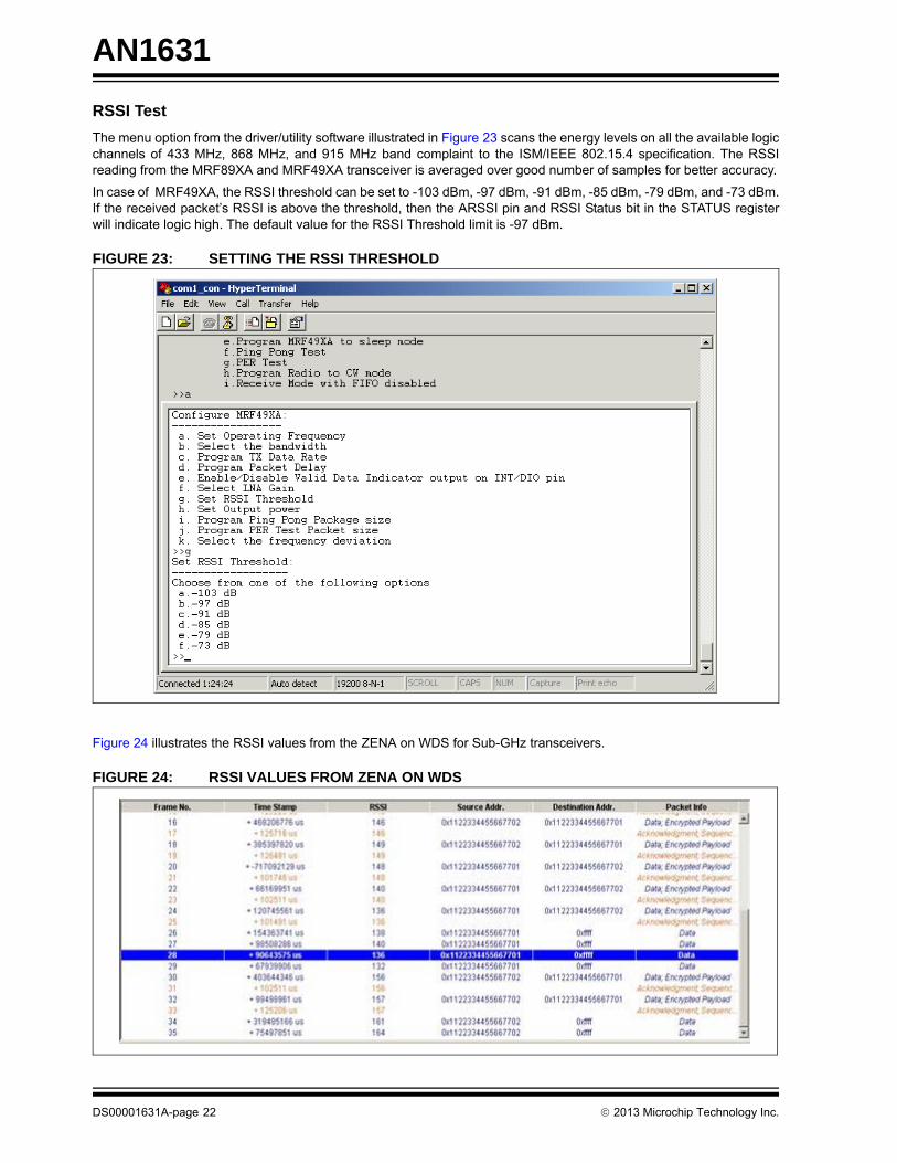
RSSI Test
The menu option from the driver/utility software illustrated in Figure 23 scans the energy levels on all the available logic channels of 433 MHz, 868 MHz, and 915 MHz band complaint to the ISM/IEEE 802.15.4 specification. The RSSI reading from the MRF89XA and MRF49XA transceiver is averaged over good number of samples for better accuracy.
In case of MRF49XA, the RSSI threshold can be set to -103 dBm, -97 dBm, -91 dBm, -85 dBm, -79 dBm, and -73 dBm. If the received packet’s RSSI is above the threshold, then the ARSSI pin and RSSI Status bit in the STATUS register will indicate logic high. The default value for the RSSI Threshold limit is -97 dBm.
FIGURE 23: SETTING THE RSSI THRESHOLD
Figure 24 illustrates the RSSI values from the ZENA on WDS for Sub-GHz transceivers.
FIGURE 24: RSSI VALUES FROM ZENA ON WDS
DS00001631A-page 22 2013 Microchip Technology Inc.
AN1631
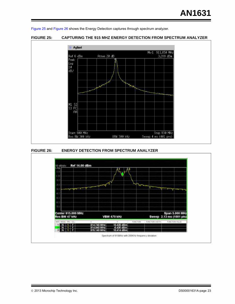
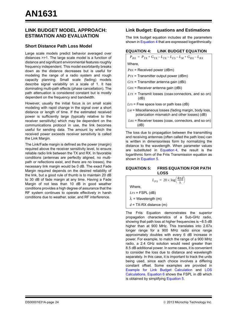
Figure 25 and Figure 26 shows the Energy Detection captures through spectrum analyzer.
FIGURE 25: CAPTURING THE 915 MHZ ENERGY DETECTION FROM SPECTRUM ANALYZER
FIGURE 26: ENERGY DETECTION FROM SPECTRUM ANALYZER
2013 Microchip Technology Inc. DS00001631A-page 23
AN1631
LINK BUDGET MODEL APPROACH: ESTIMATION AND EVALUATION
Short Distance Path Loss Model
Large scale models predict behavior averaged over distances >>1. The large scale model is a function of distance and significant environmental features roughly frequency independent. This model exorbitantly breaks down as the distance decreases but is useful for modeling the range of a radio system and rough capacity planning. Small scale (fading) models describe signal variability on a scale of 1. It has dominating multi-path effects (phase cancellation). The path attenuation is considered constant but is mostly dependent on the frequency and bandwidth.
However, usually the initial focus is on small scale modeling with rapid change in the signal over a short distance or length of time. If the estimated received power is sufficiently large (typically relative to the receiver sensitivity) which may be dependent on the communications protocol in use, the link becomes useful for sending data. The amount by which the received power exceeds receiver sensitivity is called the Link Margin.
The Link/Fade margin is defined as the power (margin) required above the receiver sensitivity level, to ensure reliable radio link between the TX and RX. In favorable conditions (antennas are perfectly aligned, no multi-path or reflections exist, and there are no losses), the necessary link margin would be 0 dB. The exact Fade Margin required depends on the desired reliability of the link, but a good rule of thumb is to maintain 20 dB to 30 dB of fade margin at any time. Having a Fade Margin of not less than 10 dB in good weather conditions provides a high degree of assurance that the RF system continues to operate effectively in harsh conditions due to weather, solar, and RF interference.
Link Budget: Equations and Estimations
The link budget equation includes all the parameters shown in Equation 4 that are expressed logarithmically.
EQUATION 4: LINK BUDGET EQUATIONPRX PTX GTX LTX– LFS– LM– GRX LRX–+ +=
Where,
PRX = Received power (dBm)
PTX = Transmitter output power (dBm)
GTX = Transmitter antenna gain (dBi)
GRX = Receiver antenna gain (dBi)
LTX = Transmit losses (coax connectors, and so on) (dB)
LFS = Free space loss or path loss (dB)
LM = Miscellaneous losses (fading margin, body loss, polarization mismatch and other losses) (dB)
LRX = Receiver losses (coax, connectors, and so on) (dB)
The loss due to propagation between the transmitting and receiving antennas (often called the path loss) can is written in dimensionless form by normalizing the distance to the wavelength. When parameter values are substituted in Equation 4, the result is the logarithmic form of the Friis Transmission equation as shown in Equation 5.
EQUATION 5: FRIIS EQUATION FOR PATH LOSS
Where,
LFS = FSPL (dB)
= Wavelength (m)
d = TX-RX distance (m)
LFS 204d
---------- log=
The Friis Equation demonstrates the superior propagation characteristics of a Sub-GHz radio, showing that path loss at higher frequencies is ~8.5 dB higher than at 900 MHz. This translates into 2.67x longer range for a 900 MHz radio since range approximately doubles with every 6 dB increase in power. For example, to match the range of a 900 MHz radio, a 2.4 GHz solution would need greater than 8.5 dB additional power. In some cases, it is convenient to consider the loss due to distance and wavelength separately. In this case, it is important to track the units being used, since each choice involves a differing constant offset. Some examples are provided in Example for Link Budget Calculation and LOS Calculations. Equation 6 shows the FSPL in dB which is obtained by simplifying Equation 5.
DS00001631A-page 24 2013 Microchip Technology Inc.
AN1631
EQUATION 6: FSPL IN DB
Where,
d = Distance (m)
f = Frequency (MHz)
K = Constant has a value of -147.55 for the units used for d and f
FSPL dB 20 d log 20 f log K+ +=
Table 12 shows FSPL (dB) for different distances of Sub-GHz frequencies. From Table 12, it implies that the variation of FSPL (dB) is almost linear for the distance specified, and the values can be interpolated or extrapolated based on the distance <1 km or >50 km.
TABLE 12: DISTANCE-FSPL CHART FOR 900 MHZ BAND
Distance (km) FSPL (dB)
1 91.53
2 97.56
3 101.08
4 103.58
5 105.51
10 111.53
20 117.56
30 121.08
40 123.58
50 125.51
EXAMPLE FOR LINK BUDGET CALCULATION
As an example, it is good to estimate the feasibility of a 1 km link (range) with RF node 1 and RF node 2 with any of the Sub-GHz modules. Consider MRF89XAM9A modules with 10 dBm output power. Node 1 is connected to an omni-directional PCB antenna with 1 dBi gain, while node 2 is also connected to a similar PCB antenna with 1 dBi gain. The transmitting power of node 1 is 10 dBm (or 1 mW) and its sensitivity is -107 dBm. The transmitting power of node 2 is similar and is 10 dBm (or 1 mW) with a similar sensitivity as node 1, its sensitivity is -107 dBm. The cables are short and are approximated with a loss of 1 dB on each side.
Equation 7 shows adding all the gains and subtracting all the losses from node 1 to node 2 link considering only the free space loss for a path loss of 1 km link.
EQUATION 7: GAIN AND PATH LOSS - NODE 1 TO NODE 2 USING MRF89XAM9A
TotalGain 10dB=
PathLoss 10 20 1000 log+ 70dB= =
10dB 70dB– 60 dB–=
Subtracting path loss from the total gain,
10dBm TXPowerRadio1 1dBi AntennaGainRadio1 1 dB CableLossesRadio1 –
1 dBi AntennaGainRadio2 1 dB CableLossesRadio2 –
+
+
The path loss for a kilometer link, considering only the free space loss is:
Since -60 dB is greater than the minimum receive sensitivity of node 2 (-107 dBm), the signal level is just enough for node 2 to communicate with node 1. From Equation 7, there is 47 dB margin (107 dB - 60 dB) which is suitable for good transmission under good weather conditions, but may not be enough to protect against harsh weather conditions.
2013 Microchip Technology Inc. DS00001631A-page 25
AN1631
Equation 8 calculates the link from node 2 back to the node 1.
EQUATION 8: GAIN AND PATH LOSS - NODE 2 TO NODE 1 USING MRF89XAM9A
TotalGain 10dB=
10dB 70dB– 60dB–=
The path loss is the same on the return path. Therefore, received signal on the Node 1 side is:
10dBm TXPowerRadio2 1 dBi AntennaGainRadio2 1 dB CableLossRadio2 – 1 dBi AntennaGainRadio1 1 dB CableLossRadio1 –
+ +
The path loss is same on the return path. Therefore, the received signal level on node 1 side is -60 dB. Since the receive sensitivity of node 1 is -102 dBm, this leaves a Fade Margin of 42 dB (102 dB - 60 dB). Additionally there are losses due to environment (fading) even at LOS and could further reduce by 20 dB which is within the requirement for communication without any additional gain. However, if node 2 is MRF89XAM9A module with 10 dBm gain (output power), calculating the link from node 2 back to the node 1, is as shown in Equation 9.
EQUATION 9: GAIN AND PATH LOSS: NODE 1 TO NODE 2 USING MRF89XAM9A
TotalGain 0 dB=
PathLoss 0 20 1000 log 60 dB=+=
The path loss for a kilometer link, considering only the free space loss is:
0 dBm TXPowerRadio2 1 dBi AntennaGainRadio2 1 dB CableLossRadio2 – 1 dBi AntennaGainRadio1 1 dB CableLossRadio1 –
+ +
Subtracting the path loss from total gain (path loss is same on the return path), the received signal level on node 1 side is shown in Equation 9. Equation 10 provides the total gain and path loss calculation from node 2 to node 1 for MRF89XAM9A module.
EQUATION 10: GAIN AND PATH LOSS - NODE 2 TO NODE 1 USING MRF89XAM9A
LinkM inarg ReceivedPower ReceiveSensitivity–=
0 dBm 60 dB– 60 dBm–=
Since the receive sensitivity of node 1 is -107 dBm, this leaves a Fade margin of 47 dBm (107 dB - 60 dB). Additionally there are losses due to environment (fading) even at LOS and can further reduce by 20 dB which communicates only with some additional gain of 20 dB to 25 dB.
DS00001631A-page 26 2013 Microchip Technology Inc.
AN1631
LOS CALCULATIONS
FSPL depends on two parameters: frequency of radio signals and wireless transmission distance as shown in Equation 11.
EQUATION 11: FSPL EQUATION
LFS dB 20 f log 20 d log+ 147.55–=
Where,
f = Frequency is in MHz
d = Distance is in meters
For example, using Equation 11 for distance = 350m for the MRF89XAM9A module (1 mW, 0 dBm) operating with a frequency of 915 MHz, the calculation is shown in Equation 12.
EQUATION 12:
FSPL dB 20 f log 20 d log 147.55–+=
20 915 log 20 350 log 147.55–+=
59.23 50.88 147.55–+ = 37.44dBm=
FSPL CALCULATION
From the fade margin equation, FSPL can also be computed as shown in Equation 13.
EQUATION 13: FADE MARGIN CALCULATION
FSPL dB TxPower TxCableLoss– TxAntennaGain RxAntennaGain
RxCableLoss– RxSensitivity– FadeM inarg–
+ +=
0 dBm 1 dB– 1 dBi 1 dBi 1 dB– 107– 82.1–+ + 189dBm==
FROM FSPL
With the FSPL equations shown in Equation 12 and Equation 13, the distance (m) can be calculated as shown in Equation 14.
EQUATION 14: DISTANCE CALCULATION FROM FSPL
LFS dB 20 frequency log 20 dis cetan log+ 147.55–=
Where, frequency is in MHz and distance is in meters.
20 dis cetan log 20– frequency log LFS dB 147.55+ +=
Substituting f = 915 MHz, K = -147.55 and LFS (dB) = 37.43, gives d = 332m from Equation 11. Hence, assuming Lfs (dB) is in between 25 dB-35dB provides good radio range.
Note: Some parameters such as Fade Margin inthe calculations are calculated/deducedusing the link budget calculator.
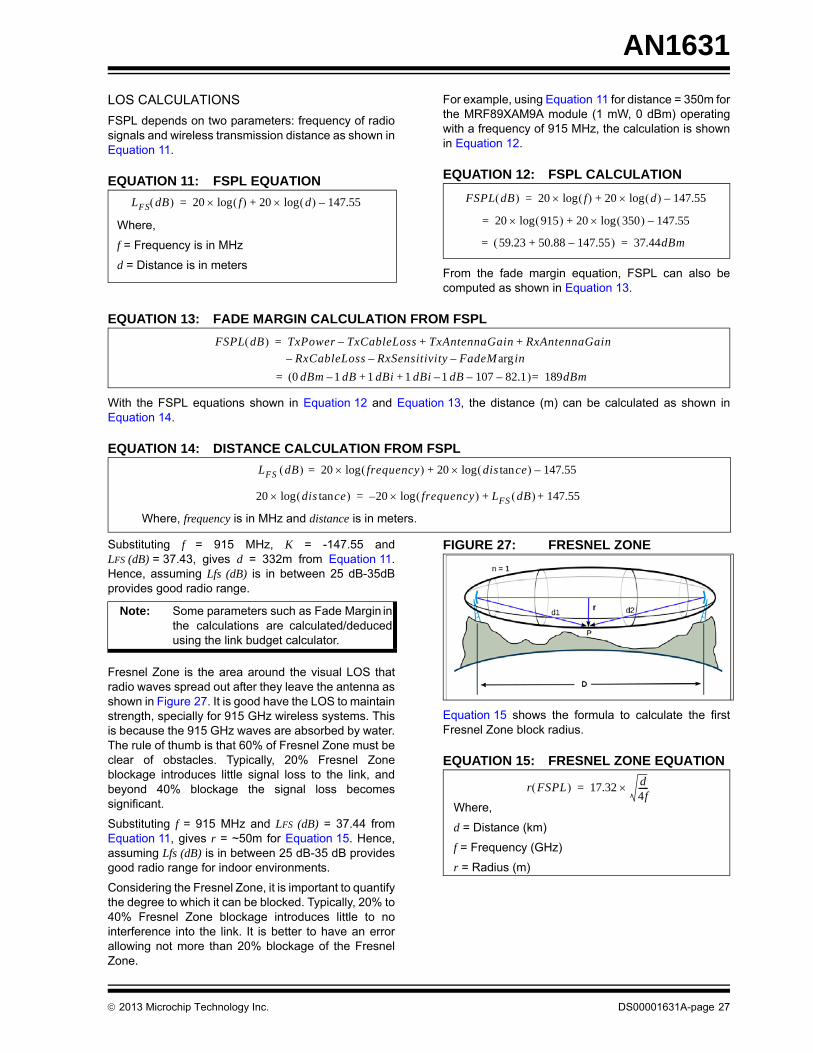
Fresnel Zone is the area around the visual LOS that radio waves spread out after they leave the antenna as shown in Figure 27. It is good have the LOS to maintain strength, specially for 915 GHz wireless systems. This is because the 915 GHz waves are absorbed by water. The rule of thumb is that 60% of Fresnel Zone must be clear of obstacles. Typically, 20% Fresnel Zone blockage introduces little signal loss to the link, and beyond 40% blockage the signal loss becomes significant.
Substituting f = 915 MHz and LFS (dB) = 37.44 from Equation 11, gives r = ~50m for Equation 15. Hence, assuming Lfs (dB) is in between 25 dB-35 dB provides good radio range for indoor environments.
Considering the Fresnel Zone, it is important to quantify the degree to which it can be blocked. Typically, 20% to 40% Fresnel Zone blockage introduces little to no interference into the link. It is better to have an error allowing not more than 20% blockage of the Fresnel Zone.
FIGURE 27: FRESNEL ZONE
Equation 15 shows the formula to calculate the first Fresnel Zone block radius.
EQUATION 15:
Where,
d = Distance (km)
f = Frequency (GHz)
r = Radius (m)
r FSPL 17.32 d4f-----=
FRESNEL ZONE EQUATION
2013 Microchip Technology Inc. DS00001631A-page 27
AN1631
NON-LOS CALCULATIONS
The propagation losses for indoors can be significantly higher in building obstructions such as walls and ceilings. This occurs because of a combination of attenuation by walls and ceilings, and blockage due to equipment, furniture and human intervention:
• Trees attenuate around 6 dB to 12 dB of loss per tree in the direct path. This attenuation depends on the size and type of tree.
• A 2x4 wood-stud/dry wall on both sides results in about 6 dB loss per wall.
• Older buildings may have even greater internal losses than new buildings due to materials and LOS issues.
• Concrete walls account to 6 dB to 10 dB depending upon the construction.
• Building floors account 12 dB to 27 dB of loss. The concrete and steel floors attenuate more compared to the wooden floors.
• Mirrored walls have very high loss because the reflective coating is conductive.
The Fresnel Zone is sometimes a good indication of an indoor environment range measurement. Generally, the LOS propagation is valid only for about first 3m. Beyond 3m, the indoor propagation losses can go up to 30 dB per 30m in dense office environments. Conservatively, it overstates the path loss in most cases. Actual propagation losses may vary significantly depending on the building construction, structure and layout.
Some of the possible reasons for propagation losses through the Fresnel zone are:
• Collisions with other transmitters
• Weak Error Vector Magnitude (EVM) from transmitter generally in the range of 20% to 24% rms
• Reflections from every object (for example, moving objects or people).
Long Distance Path Loss Model
Long distance path loss can be represented by the path loss exponent (n), whose value is normally in the range of 2 to 4 (where, 2 is for propagation in free space and 4is for relatively loss environments). In environments such as buildings, stadiums and other indoor environments, the path loss exponent can reach values in the range of 4 to 6. However, a tunnel may act as a wave guide resulting in a path loss exponent <2.
PATH LOSS AND DISTANCE CALCULATIONS
Path loss is expressed in dB and is calculated as shown in Equation 16.
EQUATION 16: LONG DISTANCE PATH LOSS MODEL EQUATION
Where,
L = Path loss (dB) is the path loss exponent
d = Distance (m) between TX and RX
C = Constant which accounts for system losses
n = Path loss/scattering exponent
L 10 n d log C+=
RF engineers use Equation 6 for the calculation of path loss (dB) between two isotropic antennas in free space. From Long Distance Path Loss model, the calculated range values are approximated to the measured range values. The results obtained for ranges at 915 GHz (26th channel) are in-line with the measured values. This model for simple point to point communication perfectly suits the LOS and obstructed ranges with approximations. However, the model is also used for multipoint obstructions.
Measured data from LOS calculations offers a mode to understand the Path Loss model used for calculating the transmission distance. The calculated versus measured results demonstrate the limitations of the free space model. Results from even terrains versus level surfaces are better modeled with a path loss coefficient of 2.1 and 2.2, respectively. Better range/ performance are possible using the range models specified in Range Measurement Environments.
Range results and path loss calculations are useful in determining the link budgets. For example, MRF89XA (with 0 dBm) demonstrates the capability to reach 65m (non-LOS) to 120m (LOS) without the use of on-board PA/LNA. The accommodative range with exceptional coverage is predicted to be in the order of 100m to 200m when applying the FSPL and fade margin equations. Similarly, MRF89XA (with 10 dBm) touches a range of 120m (non-LOS) to 650m (LOS) with the use of on-board PA/LNA. The accommodative range with exceptional coverage is predicted to be in the order of 160m to a kilometer when applying the FSPL and fade margin equations for longer ranges.
DS00001631A-page 28 2013 Microchip Technology Inc.
AN1631
RANGE PERFORMANCE SUMMARY
This section summarizes the measured range and other performance parameters with the estimations done through a range/link budget model.
A common rule of thumb used in the RF design is 6 dB increase in the link budget results when doubling the transmission distance. This rule holds true for the FSPL model, but is more optimistic and does not hold true for more realistic models. In few cases, it may take in excess of 15 dB increase in the link budget to double the transmission distance. Most antennas broadcast in a horizontal pattern, so vertical separation is more meaningful than the horizontal separation. The measured antenna radiation patterns are useful when applying the range models.
The range measurements also show that the terrain profiles have a significant effect on range performance. In Table 5, it shows the differences in measurements between the two selected terrains. All of these factors randomly combine to create extremely complex scenarios. Various outdoor and indoor propagation models have been created to address the concern. The outoor radio channel differs from the indoor channel because the indoor channel has shorter distances to cover, higher path loss variability and greater variance in the received signal power. However, variability in the received signal power is insignificant for stationary wireless devices. Building layout, type and construction materials strongly affect the indoor propagation.
The following variables must be known when applying the range models for the path loss formula:
• Gains of the TX and RX antennas
• Power received at the RX input
• Power delivered by the TX into the antenna
The other factors that may affect range performance in addition to the antenna radiation patterns of the TX and RX are as follows:
• Antenna losses (due to matching network design)
• Multi-path fading
• Interference of other propagating signals
• Background noise
The range measurements detailed in Range Measurement Conditions and Results quantify the improvements made by the following factors:
• Setting the maximum internal PA output power to maximum
• Using an LNA (match its input for the minimum noise required impedance and not for minimum insertion loss)
• Configuring for the highest value of receiver sensitivity
• Orienting the antenna in the upright position
• Designing the application board with any type of antennas which include patch, wire or whip antenna
• Setting the transmitter in the LOS of the receiver for open field tests
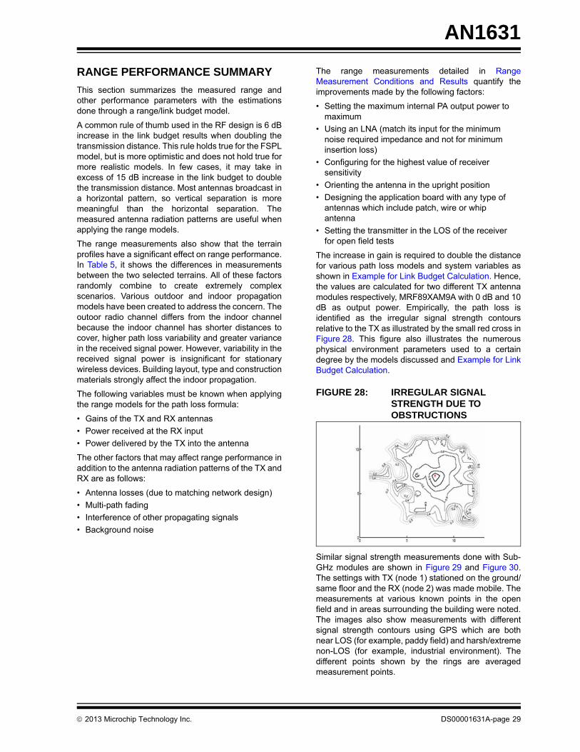
The increase in gain is required to double the distance for various path loss models and system variables as shown in Example for Link Budget Calculation. Hence, the values are calculated for two different TX antenna modules respectively, MRF89XAM9A with 0 dB and 10 dB as output power. Empirically, the path loss is identified as the irregular signal strength contours relative to the TX as illustrated by the small red cross in Figure 28. This figure also illustrates the numerous physical environment parameters used to a certain degree by the models discussed and Example for Link Budget Calculation.
FIGURE 28: IRREGULAR SIGNAL STRENGTH DUE TO OBSTRUCTIONS
Similar signal strength measurements done with Sub-GHz modules are shown in Figure 29 and Figure 30. The settings with TX (node 1) stationed on the ground/same floor and the RX (node 2) was made mobile. The measurements at various known points in the open field and in areas surrounding the building were noted. The images also show measurements with different signal strength contours using GPS which are both near LOS (for example, paddy field) and harsh/extreme non-LOS (for example, industrial environment). The different points shown by the rings are averaged measurement points.
2013 Microchip Technology Inc. DS00001631A-page 29
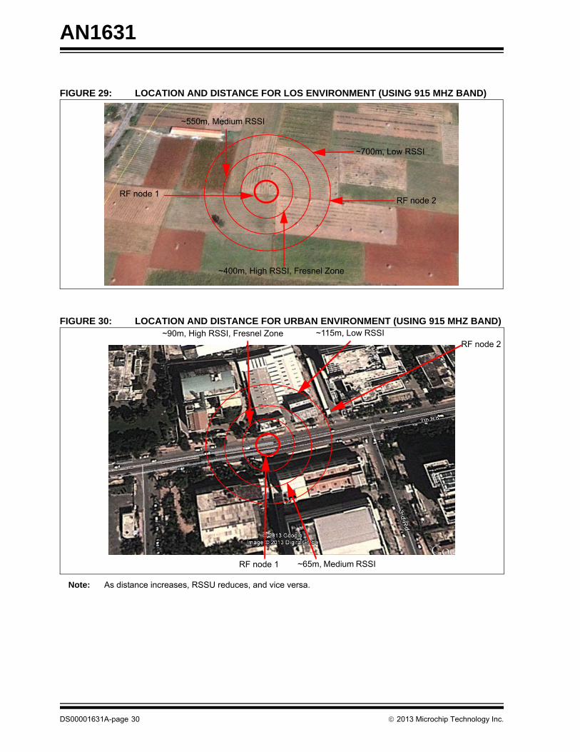
AN1631
FIGURE 29:
RF node 1RF node 2
~700m, Low RSSI
~550m, Medium RSSI
~400m, High RSSI, Fresnel Zone
LOCATION AND DISTANCE FOR LOS ENVIRONMENT (USING 915 MHZ BAND)
FIGURE 30:
RF node 2
RF node 1 ~65m, Medium RSSI
~90m, High RSSI, Fresnel Zone ~115m, Low RSSILOCATION AND DISTANCE FOR URBAN ENVIRONMENT (USING 915 MHZ BAND)
Note: As distance increases, RSSU reduces, and vice versa.
DS00001631A-page 30 2013 Microchip Technology Inc.
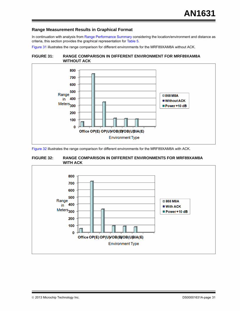
AN1631
Range Measurement Results in Graphical Format
In continuation with analysis from Range Performance Summary considering the location/environment and distance as criteria, this section provides the graphical representation for Table 5.
Figure 31 illustrates the range comparison for different environments for the MRF89XAM8A without ACK.
FIGURE 31: RANGE COMPARISON IN DIFFERENT ENVIRONMENT FOR MRF89XAM8A WITHOUT ACK
Figure 32 illustrates the range comparison for different environments for the MRF89XAM8A with ACK.
FIGURE 32: RANGE COMPARISON IN DIFFERENT ENVIRONMENTS FOR MRF89XAM8A WITH ACK
2013 Microchip Technology Inc. DS00001631A-page 31
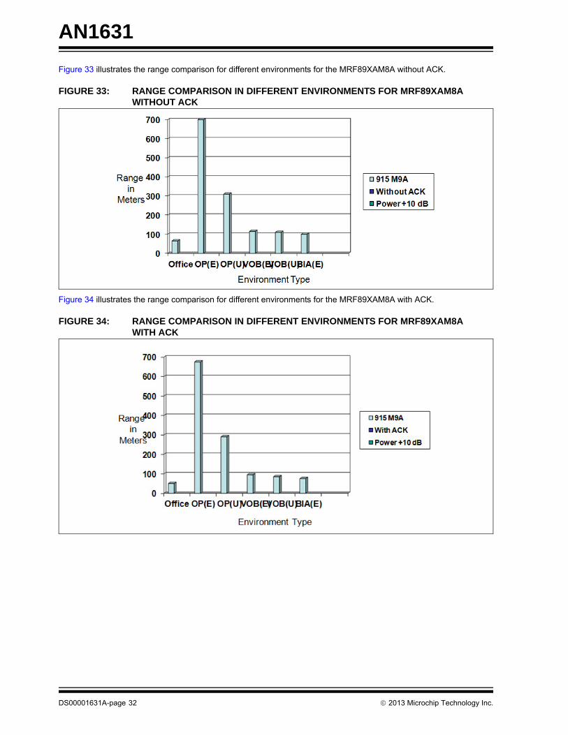
AN1631
Figure 33 illustrates the range comparison for different environments for the MRF89XAM8A without ACK.
FIGURE 33: RANGE COMPARISON IN DIFFERENT ENVIRONMENTS FOR MRF89XAM8A WITHOUT ACK
Figure 34 illustrates the range comparison for different environments for the MRF89XAM8A with ACK.
FIGURE 34: RANGE COMPARISON IN DIFFERENT ENVIRONMENTS FOR MRF89XAM8A WITH ACK
DS00001631A-page 32 2013 Microchip Technology Inc.
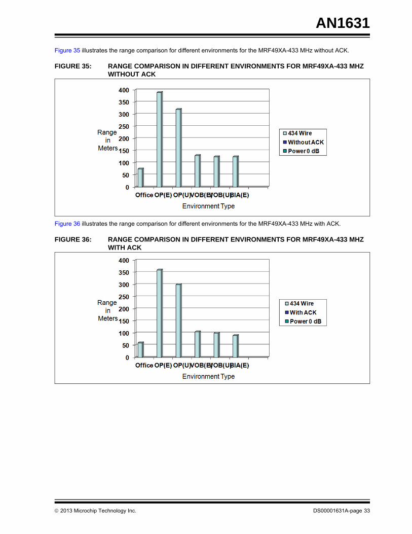
AN1631
Figure 35 illustrates the range comparison for different environments for the MRF49XA-433 MHz without ACK.
FIGURE 35: RANGE COMPARISON IN DIFFERENT ENVIRONMENTS FOR MRF49XA-433 MHZ WITHOUT ACK
Figure 36 illustrates the range comparison for different environments for the MRF49XA-433 MHz with ACK.
FIGURE 36: RANGE COMPARISON IN DIFFERENT ENVIRONMENTS FOR MRF49XA-433 MHZ WITH ACK
2013 Microchip Technology Inc. DS00001631A-page 33
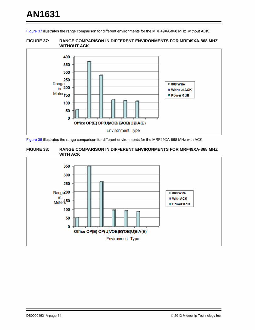
AN1631
Figure 37 illustrates the range comparison for different environments for the MRF49XA-868 MHz without ACK.
FIGURE 37: RANGE COMPARISON IN DIFFERENT ENVIRONMENTS FOR MRF49XA-868 MHZ WITHOUT ACK
Figure 38 illustrates the range comparison for different environments for the MRF49XA-868 MHz with ACK.
FIGURE 38: RANGE COMPARISON IN DIFFERENT ENVIRONMENTS FOR MRF49XA-868 MHZ WITH ACK
DS00001631A-page 34 2013 Microchip Technology Inc.
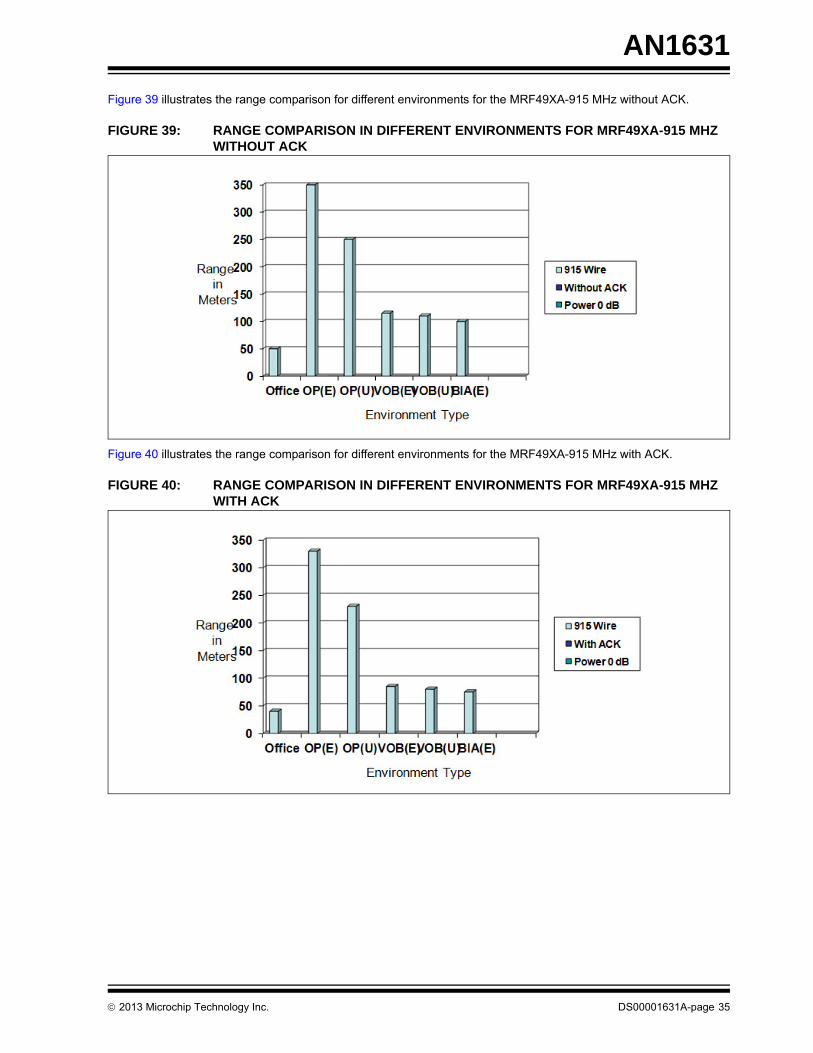
AN1631
Figure 39 illustrates the range comparison for different environments for the MRF49XA-915 MHz without ACK.
FIGURE 39: RANGE COMPARISON IN DIFFERENT ENVIRONMENTS FOR MRF49XA-915 MHZ WITHOUT ACK
Figure 40 illustrates the range comparison for different environments for the MRF49XA-915 MHz with ACK.
FIGURE 40: RANGE COMPARISON IN DIFFERENT ENVIRONMENTS FOR MRF49XA-915 MHZ WITH ACK
2013 Microchip Technology Inc. DS00001631A-page 35
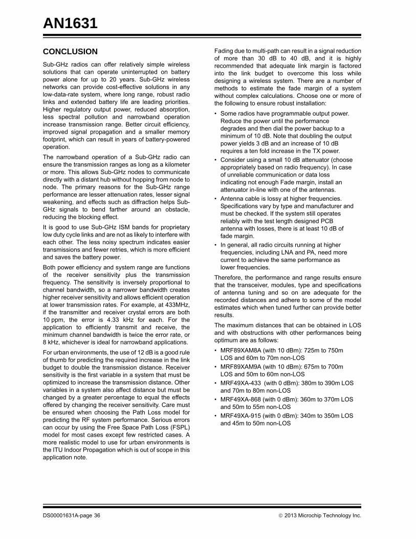
AN1631
CONCLUSION
Sub-GHz radios can offer relatively simple wireless solutions that can operate uninterrupted on battery power alone for up to 20 years. Sub-GHz wireless networks can provide cost-effective solutions in any low-data-rate system, where long range, robust radio links and extended battery life are leading priorities. Higher regulatory output power, reduced absorption, less spectral pollution and narrowband operation increase transmission range. Better circuit efficiency, improved signal propagation and a smaller memory footprint, which can result in years of battery-powered operation.
The narrowband operation of a Sub-GHz radio can ensure the transmission ranges as long as a kilometer or more. This allows Sub-GHz nodes to communicate directly with a distant hub without hopping from node to node. The primary reasons for the Sub-GHz range performance are lesser attenuation rates, lesser signal weakening, and effects such as diffraction helps Sub-GHz signals to bend farther around an obstacle, reducing the blocking effect.
It is good to use Sub-GHz ISM bands for proprietary low duty cycle links and are not as likely to interfere with each other. The less noisy spectrum indicates easier transmissions and fewer retries, which is more efficient and saves the battery power.
Both power efficiency and system range are functions of the receiver sensitivity plus the transmission frequency. The sensitivity is inversely proportional to channel bandwidth, so a narrower bandwidth creates higher receiver sensitivity and allows efficient operation at lower transmission rates. For example, at 433MHz, if the transmitter and receiver crystal errors are both 10 ppm, the error is 4.33 kHz for each. For the application to efficiently transmit and receive, the minimum channel bandwidth is twice the error rate, or 8 kHz, whichever is ideal for narrowband applications.
For urban environments, the use of 12 dB is a good rule of thumb for predicting the required increase in the link budget to double the transmission distance. Receiver sensitivity is the first variable in a system that must be optimized to increase the transmission distance. Other variables in a system also affect distance but must be changed by a greater percentage to equal the effects offered by changing the receiver sensitivity. Care must be ensured when choosing the Path Loss model for predicting the RF system performance. Serious errors can occur by using the Free Space Path Loss (FSPL) model for most cases except few restricted cases. A more realistic model to use for urban environments is the ITU Indoor Propagation which is out of scope in this application note.
Fading due to multi-path can result in a signal reduction of more than 30 dB to 40 dB, and it is highly recommended that adequate link margin is factored into the link budget to overcome this loss while designing a wireless system. There are a number of methods to estimate the fade margin of a system without complex calculations. Choose one or more of the following to ensure robust installation:
• Some radios have programmable output power. Reduce the power until the performance degrades and then dial the power backup to a minimum of 10 dB. Note that doubling the output power yields 3 dB and an increase of 10 dB requires a ten fold increase in the TX power.
• Consider using a small 10 dB attenuator (choose appropriately based on radio frequency). In case of unreliable communication or data loss indicating not enough Fade margin, install an attenuator in-line with one of the antennas.
• Antenna cable is lossy at higher frequencies. Specifications vary by type and manufacturer and must be checked. If the system still operates reliably with the test length designed PCB antenna with losses, there is at least 10 dB of fade margin.
• In general, all radio circuits running at higher frequencies, including LNA and PA, need more current to achieve the same performance as lower frequencies.
Therefore, the performance and range results ensure that the transceiver, modules, type and specifications of antenna tuning and so on are adequate for the recorded distances and adhere to some of the model estimates which when tuned further can provide better results.
The maximum distances that can be obtained in LOS and with obstructions with other performances being optimum are as follows:
• MRF89XAM8A (with 10 dBm): 725m to 750m LOS and 60m to 70m non-LOS
• MRF89XAM9A (with 10 dBm): 675m to 700m LOS and 50m to 60m non-LOS
• MRF49XA-433 (with 0 dBm): 380m to 390m LOS and 70m to 80m non-LOS
• MRF49XA-868 (with 0 dBm): 360m to 370m LOS and 50m to 55m non-LOS
• MRF49XA-915 (with 0 dBm): 340m to 350m LOS and 45m to 50m non-LOS
DS00001631A-page 36 2013 Microchip Technology Inc.
AN1631
REFERENCES
• “MRF49XA Radio Utility Program” (AN1309)
• “MRF89XA Radio Utility Program” (AN1340)
• “Microchip MiWi™ Wireless Networking Protocol Stack” (DS01066)
• “Microchip MiWi™ P2P Wireless Protocol” (DS01204)
• “MRF24WB0M Indoor and Outdoor Antenna Range Testing” (DS01363)
• “Wireless Communications Principles and Practices”, T.S. Rappaport, 2002, Prentice-Hall
• “Introduction to RF Propagation”, John S. Seybold, 2005, Wiley
• “Modern Communications Systems”, Couch, LeonW., Prentice-Hall, Inc., Englewood Cliffs, NJ, 1995.
• “Digital Communications Systems”, Peebles, Peyton Z. Prentice-Hall, Inc., Englewood Cliffs, NJ, 1987.
• “Digital Communications”, Proakis, John G., Second Edition, McGraw-Hill, New York, NY, 1989 4. Spread Spectrum Systems, Dixon, Robert C., Third Edition, John Wiley
• Link Budget Calculator
(http://www.afar.net/rf-link-budget-calculator)
• (http://www.bb-elec.com/Learning-Center/All-White-Papers/Wireless-Cellular/10-Commandments-of-Wireless-Communications.aspx)
2013 Microchip Technology Inc. DS00001631A-page 37
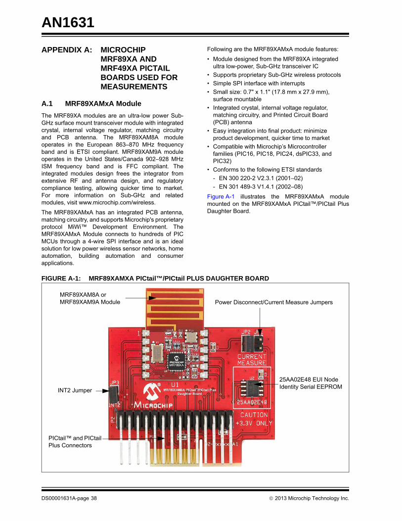
AN1631
APPENDIX A: MICROCHIP MRF89XA AND MRF49XA PICTAIL BOARDS USED FOR MEASUREMENTS
A.1 MRF89XAMxA Module
The MRF89XA modules are an ultra-low power Sub-GHz surface mount transceiver module with integrated crystal, internal voltage regulator, matching circuitry and PCB antenna. The MRF89XAM8A module operates in the European 863–870 MHz frequency band and is ETSI compliant. MRF89XAM9A module operates in the United States/Canada 902–928 MHz ISM frequency band and is FFC compliant. The integrated modules design frees the integrator from extensive RF and antenna design, and regulatory compliance testing, allowing quicker time to market. For more information on Sub-GHz and related modules, visit www.microchip.com/wireless.
The MRF89XAMxA has an integrated PCB antenna, matching circuitry, and supports Microchip's proprietary protocol MiWi™ Development Environment. The MRF89XAMxA Module connects to hundreds of PIC MCUs through a 4-wire SPI interface and is an ideal solution for low power wireless sensor networks, home automation, building automation and consumer applications.
Following are the MRF89XAMxA module features:
• Module designed from the MRF89XA integrated ultra low-power, Sub-GHz transceiver IC
• Supports proprietary Sub-GHz wireless protocols
• Simple SPI interface with interrupts
• Small size: 0.7" x 1.1" (17.8 mm x 27.9 mm), surface mountable
• Integrated crystal, internal voltage regulator, matching circuitry, and Printed Circuit Board (PCB) antenna
• Easy integration into final product: minimize product development, quicker time to market
• Compatible with Microchip’s Microcontroller families (PIC16, PIC18, PIC24, dsPIC33, and PIC32)
• Conforms to the following ETSI standards
- EN 300 220-2 V2.3.1 (2001–02)
- EN 301 489-3 V1.4.1 (2002–08)
Figure A-1 illustrates the MRF89XAMxA module mounted on the MRF89XAMxA PICtail™/PICtail Plus Daughter Board.
FIGURE A-1: MRF89XAMXA PICtail™/PICtail PLUS DAUGHTER BOARD
MRF89XAM8A or MRF89XAM9A Module Power Disconnect/Current Measure Jumpers
INT2 Jumper
PICtail™ and PICtail Plus Connectors
25AA02E48 EUI Node Identity Serial EEPROM
DS00001631A-page 38 2013 Microchip Technology Inc.
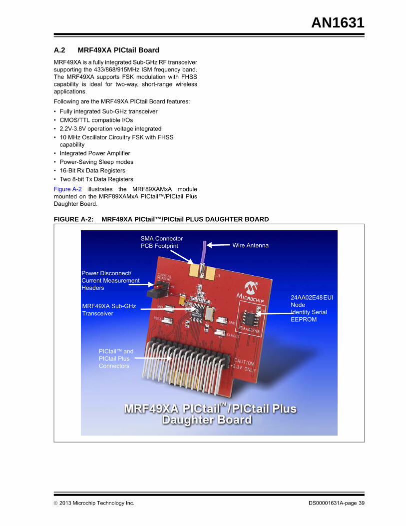
AN1631
A.2 MRF49XA PICtail Board
MRF49XA is a fully integrated Sub-GHz RF transceiver supporting the 433/868/915MHz ISM frequency band. The MRF49XA supports FSK modulation with FHSS capability is ideal for two-way, short-range wireless applications.
Following are the MRF49XA PICtail Board features:
• Fully integrated Sub-GHz transceiver
• CMOS/TTL compatible I/Os
• 2.2V-3.8V operation voltage integrated
• 10 MHz Oscillator Circuitry FSK with FHSS capability
• Integrated Power Amplifier
• Power-Saving Sleep modes
• 16-Bit Rx Data Registers
• Two 8-bit Tx Data Registers
Figure A-2 illustrates the MRF89XAMxA module mounted on the MRF89XAMxA PICtail™/PICtail Plus Daughter Board.
FIGURE A-2: MRF49XA PICtail™/PICtail PLUS DAUGHTER BOARD
SMA ConnectorPCB Footprint
Power Disconnect/Current Measurement Headers
MRF49XA Sub-GHz Transceiver
PICtail™ and PICtail Plus Connectors
Wire Antenna
24AA02E48 EUI Node Identity Serial EEPROM
2013 Microchip Technology Inc. DS00001631A-page 39
AN1631
NOTES:
DS00001631A-page 40 2013 Microchip Technology Inc.
Note the following details of the code protection feature on Microchip devices:
• Microchip products meet the specification contained in their particular Microchip Data Sheet.
• Microchip believes that its family of products is one of the most secure families of its kind on the market today, when used in the intended manner and under normal conditions.
• There are dishonest and possibly illegal methods used to breach the code protection feature. All of these methods, to our knowledge, require using the Microchip products in a manner outside the operating specifications contained in Microchip’s Data Sheets. Most likely, the person doing so is engaged in theft of intellectual property.
• Microchip is willing to work with the customer who is concerned about the integrity of their code.
• Neither Microchip nor any other semiconductor manufacturer can guarantee the security of their code. Code protection does not mean that we are guaranteeing the product as “unbreakable.”
Code protection is constantly evolving. We at Microchip are committed to continuously improving the code protection features of our products. Attempts to break Microchip’s code protection feature may be a violation of the Digital Millennium Copyright Act. If such acts allow unauthorized access to your software or other copyrighted work, you may have a right to sue for relief under that Act.
Information contained in this publication regarding device applications and the like is provided only for your convenience and may be superseded by updates. It is your responsibility to ensure that your application meets with your specifications. MICROCHIP MAKES NO REPRESENTATIONS OR WARRANTIES OF ANY KIND WHETHER EXPRESS OR IMPLIED, WRITTEN OR ORAL, STATUTORY OR OTHERWISE, RELATED TO THE INFORMATION, INCLUDING BUT NOT LIMITED TO ITS CONDITION, QUALITY, PERFORMANCE, MERCHANTABILITY OR FITNESS FOR PURPOSE. Microchip disclaims all liability arising from this information and its use. Use of Microchip devices in life support and/or safety applications is entirely at the buyer’s risk, and the buyer agrees to defend, indemnify and hold harmless Microchip from any and all damages, claims, suits, or expenses resulting from such use. No licenses are conveyed, implicitly or otherwise, under any Microchip intellectual property rights.
2013 Microchip Technology Inc.
QUALITYMANAGEMENTSYSTEMCERTIFIEDBYDNV
== ISO/TS16949==
Trademarks
The Microchip name and logo, the Microchip logo, dsPIC, FlashFlex, KEELOQ, KEELOQ logo, MPLAB, PIC, PICmicro, PICSTART, PIC32 logo, rfPIC, SST, SST Logo, SuperFlash and UNI/O are registered trademarks of Microchip Technology Incorporated in the U.S.A. and other countries.
FilterLab, Hampshire, HI-TECH C, Linear Active Thermistor, MTP, SEEVAL and The Embedded Control Solutions Company are registered trademarks of Microchip Technology Incorporated in the U.S.A.
Silicon Storage Technology is a registered trademark of Microchip Technology Inc. in other countries.
Analog-for-the-Digital Age, Application Maestro, BodyCom, chipKIT, chipKIT logo, CodeGuard, dsPICDEM, dsPICDEM.net, dsPICworks, dsSPEAK, ECAN, ECONOMONITOR, FanSense, HI-TIDE, In-Circuit Serial Programming, ICSP, Mindi, MiWi, MPASM, MPF, MPLAB Certified logo, MPLIB, MPLINK, mTouch, Omniscient Code Generation, PICC, PICC-18, PICDEM, PICDEM.net, PICkit, PICtail, REAL ICE, rfLAB, Select Mode, SQI, Serial Quad I/O, Total Endurance, TSHARC, UniWinDriver, WiperLock, ZENA and Z-Scale are trademarks of Microchip Technology Incorporated in the U.S.A. and other countries.
SQTP is a service mark of Microchip Technology Incorporated in the U.S.A.
GestIC and ULPP are registered trademarks of Microchip Technology Germany II GmbH & Co. KG, a subsidiary of Microchip Technology Inc., in other countries.
All other trademarks mentioned herein are property of their respective companies.
© 2013, Microchip Technology Incorporated, Printed in the U.S.A., All Rights Reserved.
Printed on recycled paper.
ISBN: 978-1-62077-726-8
DS00001631A-page 41
Microchip received ISO/TS-16949:2009 certification for its worldwide headquarters, design and wafer fabrication facilities in Chandler and Tempe, Arizona; Gresham, Oregon and design centers in California and India. The Company’s quality system processes and procedures are for its PIC® MCUs and dsPIC® DSCs, KEELOQ® code hopping devices, Serial EEPROMs, microperipherals, nonvolatile memory and analog products. In addition, Microchip’s quality system for the design and manufacture of development systems is ISO 9001:2000 certified.

DS00001631A-page 42 2013 Microchip Technology Inc.
AMERICASCorporate Office2355 West Chandler Blvd.Chandler, AZ 85224-6199Tel: 480-792-7200 Fax: 480-792-7277Technical Support: http://www.microchip.com/supportWeb Address: www.microchip.com
AtlantaDuluth, GA Tel: 678-957-9614 Fax: 678-957-1455
Austin, TXTel: 512-257-3370
BostonWestborough, MA Tel: 774-760-0087 Fax: 774-760-0088
ChicagoItasca, IL Tel: 630-285-0071 Fax: 630-285-0075
ClevelandIndependence, OH Tel: 216-447-0464 Fax: 216-447-0643
DallasAddison, TX Tel: 972-818-7423 Fax: 972-818-2924
DetroitNovi, MI Tel: 248-848-4000
Houston, TX Tel: 281-894-5983
IndianapolisNoblesville, IN Tel: 317-773-8323Fax: 317-773-5453
Los AngelesMission Viejo, CA Tel: 949-462-9523 Fax: 949-462-9608
New York, NY Tel: 631-435-6000
San Jose, CA Tel: 408-735-9110
Canada - TorontoTel: 905-673-0699 Fax: 905-673-6509
ASIA/PACIFICAsia Pacific OfficeSuites 3707-14, 37th FloorTower 6, The GatewayHarbour City, KowloonHong KongTel: 852-2401-1200Fax: 852-2401-3431
Australia - SydneyTel: 61-2-9868-6733Fax: 61-2-9868-6755
China - BeijingTel: 86-10-8569-7000 Fax: 86-10-8528-2104
China - ChengduTel: 86-28-8665-5511Fax: 86-28-8665-7889
China - ChongqingTel: 86-23-8980-9588Fax: 86-23-8980-9500
China - HangzhouTel: 86-571-2819-3187 Fax: 86-571-2819-3189
China - Hong Kong SARTel: 852-2943-5100 Fax: 852-2401-3431
China - NanjingTel: 86-25-8473-2460Fax: 86-25-8473-2470
China - QingdaoTel: 86-532-8502-7355Fax: 86-532-8502-7205
China - ShanghaiTel: 86-21-5407-5533 Fax: 86-21-5407-5066
China - ShenyangTel: 86-24-2334-2829Fax: 86-24-2334-2393
China - ShenzhenTel: 86-755-8864-2200 Fax: 86-755-8203-1760
China - WuhanTel: 86-27-5980-5300Fax: 86-27-5980-5118
China - XianTel: 86-29-8833-7252Fax: 86-29-8833-7256
China - XiamenTel: 86-592-2388138 Fax: 86-592-2388130
China - ZhuhaiTel: 86-756-3210040 Fax: 86-756-3210049
ASIA/PACIFICIndia - BangaloreTel: 91-80-3090-4444 Fax: 91-80-3090-4123
India - New DelhiTel: 91-11-4160-8631Fax: 91-11-4160-8632
India - PuneTel: 91-20-3019-1500
Japan - OsakaTel: 81-6-6152-7160 Fax: 81-6-6152-9310
Japan - TokyoTel: 81-3-6880- 3770 Fax: 81-3-6880-3771
Korea - DaeguTel: 82-53-744-4301Fax: 82-53-744-4302
Korea - SeoulTel: 82-2-554-7200Fax: 82-2-558-5932 or 82-2-558-5934
Malaysia - Kuala LumpurTel: 60-3-6201-9857Fax: 60-3-6201-9859
Malaysia - PenangTel: 60-4-227-8870Fax: 60-4-227-4068
Philippines - ManilaTel: 63-2-634-9065Fax: 63-2-634-9069
SingaporeTel: 65-6334-8870Fax: 65-6334-8850
Taiwan - Hsin ChuTel: 886-3-5778-366Fax: 886-3-5770-955
Taiwan - KaohsiungTel: 886-7-213-7830
Taiwan - TaipeiTel: 886-2-2508-8600 Fax: 886-2-2508-0102
Thailand - BangkokTel: 66-2-694-1351Fax: 66-2-694-1350
EUROPEAustria - WelsTel: 43-7242-2244-39Fax: 43-7242-2244-393Denmark - CopenhagenTel: 45-4450-2828 Fax: 45-4485-2829
France - ParisTel: 33-1-69-53-63-20 Fax: 33-1-69-30-90-79
Germany - DusseldorfTel: 49-2129-3766400
Germany - MunichTel: 49-89-627-144-0 Fax: 49-89-627-144-44
Germany - PforzheimTel: 49-7231-424750
Italy - Milan Tel: 39-0331-742611 Fax: 39-0331-466781
Italy - VeniceTel: 39-049-7625286
Netherlands - DrunenTel: 31-416-690399 Fax: 31-416-690340
Poland - WarsawTel: 48-22-3325737
Spain - MadridTel: 34-91-708-08-90Fax: 34-91-708-08-91
Sweden - StockholmTel: 46-8-5090-4654
UK - WokinghamTel: 44-118-921-5800Fax: 44-118-921-5820
Worldwide Sales and Service
10/28/13