Embed Size (px)
Citation preview
AN2152Applications of the Peripheral Trigger Generator (PTG)
INTRODUCTION
The Peripheral Trigger Generator (PTG) module, in 16-bitdsPIC33 devices, is a user-programmable sequencer,which is capable of generating triggers with complex inputsignal sequences to coordinate the operation of otherperipherals. This document will explain various applica-tions that use PTG in conjunction with modules, such asan Analog-to-Digital Converter (ADC), Output Compare(OC), Pulse-Width Modulator (PWM), timers and interruptcontrollers to achieve a complex sequence of events.
The PTG module supports 8-bit commands, called theStep commands, to the PTG Queue registers. Each8-bit Step command is comprised of a 4-bit commandcode and a 4-bit option field.
These commands define a sequence of events forgenerating output trigger signals to the peripherals.The Step commands can also be used to generate theinterrupt requests to the CPU.
For more information on the PTG module and itsregisters, refer to “Peripheral Trigger Generator(PTG)” (DS70669) in the “dsPIC33/PIC24 FamilyReference Manual”.
Example usage cases discussed in this document areas follows:
• Application 1: Integrated PFC and Motor Control
• Application 2: Lighting Control
• Application 3: One-Shot Pulse Generation
• Application 4: Variable Width One-Shot Pulse Generation
• Application 5: Variable Frequency Waveform Generation
• Application 6: Constant Frequency Waveform Generation
• Application 7: ADC Module Control
Key Features of the PTG
• Behavior is Step Command Driven:
- Step commands are 8 bits wide
• Commands are Stored in a Step Queue:
- Queue depth is parameterized (8-32 entries)
- Programmable Step execution time (Step delay)
• Supports the Command Sequence Loop:
- Can be nested one-level deep
- Can be conditional or unconditional loop
- Two 16-bit loop counters
• Supports 16 Hardware Input Triggers:
- Sensitive to either positive or negative edges, or a high or low level
• One sOftware Input Trigger
• Generates up to 32 Unique Output Trigger Signals
• Generates Two Types of Trigger Outputs:
- Individual
- Broadcast
• Strobed Output Port for Literal Data Values:
- 5-bit literal write (literal part of a command)
- 16-bit literal write (literal held in the PTGL0 register)
• Generates up to 16 Unique Interrupt Signals
• Two 16-Bit General Purpose Timers
• Flexible Self-Contained Watchdog Timer (WDT) to Set an Upper Limit to Trigger Wait Time
• Single Step Command Capability in Debug mode
• Selectable Clock (system, PWM or ADC)
• Programmable Clock Divider
Author: Ravikiran Shetty Microchip Technology Inc.
2016 Microchip Technology Inc. DS00002152A-page 1
AN2152
APPLICATION 1: INTEGRATED PFC AND MOTOR CONTROL
In the integrated Power Factor Correction (PFC) andmotor control application, a single Digital SignalController (DSC) device controls a Permanent MagnetSynchronous Motor (PMSM) using a Field OrientedControl (FOC) scheme, as well as the PFC converter.
This application requires three PWM channels to controlthe motor functioning and an additional PWM to controlthe PFC operation. An OC module can be used toaugment the number of PWM channels available to theapplication, even beyond the number of high-speed PWMchannels available on the device.
The PWM peripheral, in conjunction with an OC periph-eral, can be used to generate the necessary PWM signalsfor motor control and PFC operation.
However, in an application such as PFC, optimalexecution time is very important, and to achieve thisobjective, we have to achieve the following tasks withinan optimal execution time:
• Synchronizing motor control PWM and PFC PWM.
• Triggering ADC for conversion, and switching ADC channels used for motor control and PFC feedback signals.
These application requirements can be achievedeffectively using the PTG module, which can performthe following operations:
• Synchronizes high-speed PWM module and OC module.
• Generates ADC module triggers by monitoring high-speed PWM module edges.
• Monitors the “ADC conversion done” interrupt and generates appropriate interrupts, executing the FOC and digital PFC control code.
• Reduces CPU intervention, making the peripheral handling in this application core-independent.
In this application, the switching frequency of motorcontrol PWM and PFC PWM is selected such that, it isin integral multiples.
The ADC in the dsPIC® DSC has four-channel simulta-neous sampling capability. Both FOC and PFCalgorithms have their own sets of analog channels thatare to be sampled simultaneously, because the phaserelationship of these signals is important from thecontrol perspective.
In this application, the feedback signals of motor con-trol and PFC are selected such that, by alternatingbetween the ADC channel selections, both motor con-trol and PFC signals are sampled. The motor controland PFC signals can be connected to the Sample-and-Hold (S&H) circuits before triggering the ADC, basedon the edges of the PWM, by configuring CH0123SA = 0or CH123SA = 1.
As shown in Table 1, the channels are configured insuch a way that, at the end of a four-channel sampleand conversion sequence, the conversion resultsfor either FOC (if CH123SA (AD1CHS123<0>) = 0and CH0SA<4:0> (AD1CHS0<4:0>) = 13) or PFC (ifCH123SA (AD1CHS123<0>) = 1 and CH0SA<4:0>(AD1CHS0<4:0>) = 10) are available in theircorresponding ADC1 Buffer registers (ADC1BUF0 toADC1BUF3).
After setting the channel selection bits to connect the PFCfeedback signals to the Sample-and-Hold circuit of anADC, for every PFC PWM cycle, a trigger has to be gen-erated. Similarly, for every motor control PWM cycle, anADC trigger has to be generated after setting the channelselection bits to connect the motor control feedbacksignals to the Sample-and-Hold circuit of the ADC.
Hence, the PTG module is configured to generate anADC trigger by monitoring the edges of the motorcontrol PWM and PFC PWM pulses.
Note: The ADC module trigger selection cannotbe changed when ADON = 1.
TABLE 1: ANALOG CHANNEL CONNECTIONS
Sample- and-Hold
Circuit
Motor ControlCH123SA = 0; CH0SA<4:0> = 13
PFCCH123SA = 1; CH0SA<4:0> = 10
Analog Feedback SignalADC
ChannelAnalog Feedback Signal
ADC Channel
CH0 Speed Reference AN13 PFC Output Voltage AN10
CH1 Phase Current 2 AN0 AC Input Voltage AN3
CH2 Phase Current 1 AN1 NA
CH3 Bus Current AN2 AC Input Current AN6
DS00002152A-page 2 2016 Microchip Technology Inc.
AN2152
In addition, two PTG interrupts (PTG1 interrupt andPTG2 interrupt) are generated to execute the code forFOC and PFC, as shown in Figure 1.
As seen in this example application, PTG simplifies theimplementation by efficiently sequencing the use of theADC and PWMs to achieve motor control and PFCimplementation in one dsPIC33 device.
FIGURE 1: CODE EXECUTION USING PTG1/PTG2 INTERRUPTS BLOCK DIAGRAM
Output Compare
PTG
PWM Interrupt
Trigger to Start
HSPWM
Trigger to Start
ADC Conversion Done
PWM Interrupt
ADC
ADC Results ADC Results
_PTG2Interrupt(void)
{
FOC ();
}
Other Functions
(Communication,
External interface
etc.)
_PTG1Interrupt(void)
{
FOC ();
}
int main (void)
{
Clock();
Peripheral_Init();
Other Initializations();
-------------------
-----------
while ()
{
Pushbutton();
-----------
------------
}
}
2016 Microchip Technology Inc. DS00002152A-page 3
AN2152
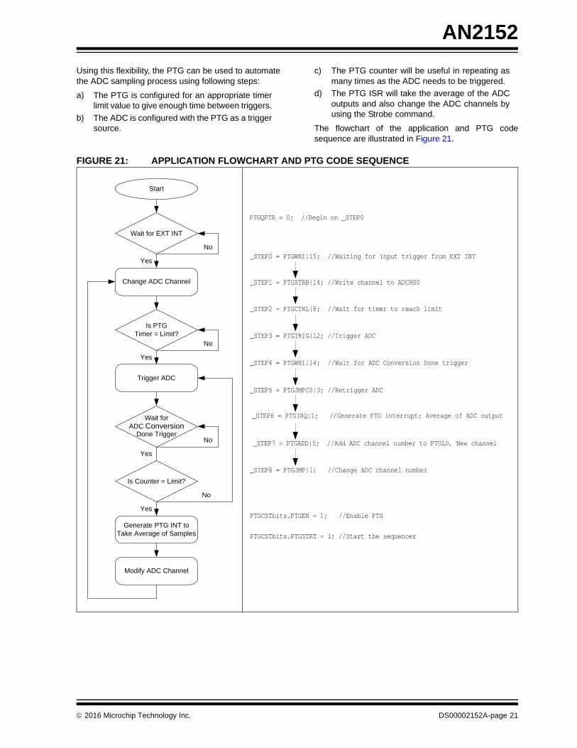
The flowchart of the application and PTG codesequence are illustrated in Figure 2.
FIGURE 2: APPLICATION FLOWCHART AND PTG CODE SEQUENCE
Start PTG
Wait for HSPWM Trigger
No
Yes
Trigger OC
Generate PTG INT to Change OC Duty
Cycle
Wait for HS PWM Trigger
Yes
No
Trigger ADC
Generate PTG INT to Run MC Code
Wait forADC Conversion
Done Trigger
Wait for OC Trigger
Yes
No
Trigger ADC
Wait forADC Conversion
Done Trigger
Generate PTG INT to Run PFC Code
Is PTG Counter = 2?
Yes
No
YesNo
No
Yes
PTGQPTR = 0; //Begin on _STEP0
_STEP0 = PTGWHI | 2;
_STEP1 = PTGCTRL | 8;
_STEP2 = PTGTRIG | 0;
_STEP3 = PTGIRQ | 0;
_STEP4 = PTGWHI | 2;
_STEP6 = PTGWHI | 14;
_STEP7 = PTGIRQ | 1;
_STEP8 = PTGWHI | 7;
_STEP9 = PTGCTRL | 9;
_STEP10 = PTGTRIG | 12;
_STEP11 = PTGWHI | 14;
_STEP12 = PTGIRQ | 2;
_STEP13 = PTGJMP0 | 8;
_STEP14 = PTGJMP| 4;
_STEP5 = PTGTRIG | 12;
PTGCSTbits.PTGEN = 1; //Enable PTG
PTGCSTbits.PTGSTRT = 1; //Start the sequencer
DS00002152A-page 4 2016 Microchip Technology Inc.
AN2152
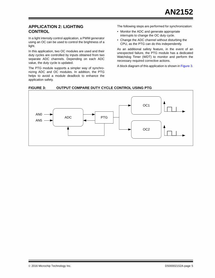
APPLICATION 2: LIGHTING CONTROL
In a light intensity control application, a PWM generatorusing an OC can be used to control the brightness of alight.
In this application, two OC modules are used and theirduty cycles are controlled by inputs obtained from twoseparate ADC channels. Depending on each ADCvalue, the duty cycle is updated.
The PTG module supports a simpler way of synchro-nizing ADC and OC modules. In addition, the PTGhelps to avoid a module deadlock to enhance theapplication safety.
The following steps are performed for synchronization:
• Monitor the ADC and generate appropriate interrupts to change the OC duty cycle.
• Change the ADC channel without disturbing the CPU, as the PTG can do this independently.
As an additional safety feature, in the event of anunexpected failure, the PTG module has a dedicatedWatchdog Timer (WDT) to monitor and perform thenecessary required corrective actions.
A block diagram of this application is shown in Figure 3.
FIGURE 3: OUTPUT COMPARE DUTY CYCLE CONTROL USING PTG
OC1
OC2
PTGADCAN0
AN5
2016 Microchip Technology Inc. DS00002152A-page 5
AN2152
Key Details of Implementation
ADC CHANNEL SELECTION
The Strobe output of the PTG module can be used towrite to the AD1CHS0 register. The PTGCTRL commandwrites the PTGL0 register contents to the AD1CHS0register. The PTGL0 register can be modified by usingthe PTGADD and PTGCOPY commands.
The ADC channels used to measure the input voltagewill be selected using the PTGL0 register and modifiedby the PTGADD and PTGCOPY commands, so that theCPU will not be interrupted.
SYNCHRONIZATION OF ADC AND OC MODULES
On some devices, since the OC module cannot triggerthe ADC and the ADC module trigger selection cannotbe changed when ADON = 1, the PTG controls theADC sampling and conversion processes. The ADCcan trigger the PTG after the conversion is done, sothat the PTG selects the next ADC channel forsampling and conversion. Hence, it synchronizes thesampling/conversion process with optimal executiontime.
The OC duty cycle can be varied by updating the OCxRand OCxRS registers. Depending on the ADC value,the duty cycle is varied.
The PTG module can generate an individual interruptpulse using the PTGIRQ command. The PTG modulecan generate up to four unique interrupt request signals.
These signals are useful for generating differentinterrupts to change the duty cycles of different OCmodules, so that executing complex functions withinone Interrupt Service Routine (ISR) can be avoided.
PTG WATCHDOG TIMER AS A SAFETY FEATURE
A Watchdog Timer (WDT), within the PTG module, willprevent a situation where the PTG waits indefinitely foran external event when executing a command whichwaits for a hardware trigger high/low state.
In this application, the PTG will wait for an “ADCconversion done” trigger. Once enabled, the WDTstarts counting when the command execution starts. Itis disabled when the command completes execution.If an expected event fails to arrive before the WDTtime-out period expires, the PTG module:
a) Aborts the (failing) command underway.
b) Halts the sequencer PTGSTRT (PTGCST<7>) = 0).
c) Sets PTGWDTO (PTGCST<6>) = 1.
d) Issues a Watchdog Timer error interrupt to theCPU.
This acts as a safety feature to recover from a situationwhere the ADC or PTG module stops working. Thesemodules can be re-initialized and restarted within theWatchdog Timer error interrupt.
DS00002152A-page 6 2016 Microchip Technology Inc.
AN2152
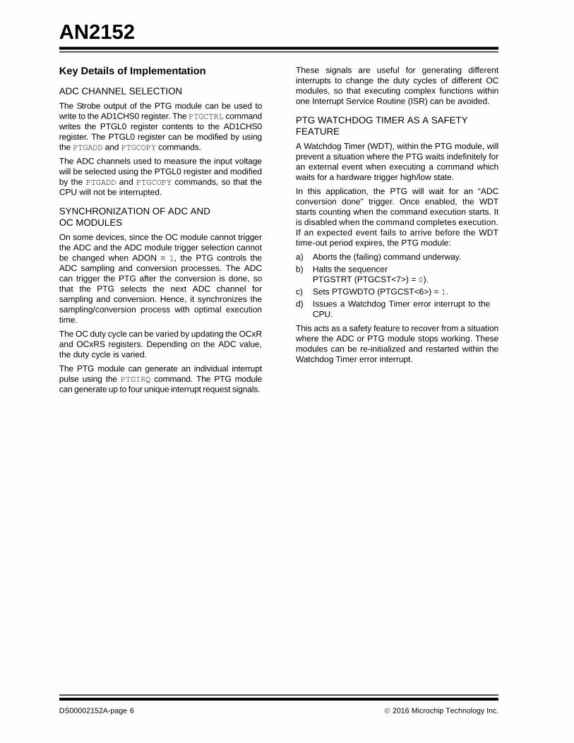
Advantages of Using PTG
a) The PTG will make the application core-independent by switching the ADC channelsand monitoring modules without the CPUmodule’s intervention.
Also, saves CPU module’s time which can beutilized for other tasks in the application.
Figure 4 and Figure 5 depict the time consump-tion, with and without PTG, and illustrates thetime available for the CPU to perform otheroperations.
b) The PTG alone will take care of all interactionswithin a module, which helps to reduce softwarecomplexity and also helps to maintain modularity.
c) The PTG module’s WDT will help to recoverfrom any catastrophic failure, thereby providinga more robust application.
d) If required, after the OC1 module triggers thePTG, the PTG, in turn, can trigger the OC2module to generate a phase-shifted output.
FIGURE 4: TIME CONSUMPTION WITHOUT PTG
FIGURE 5: TIME CONSUMPTION WITH PTG
CPU
OC2
ADC
OC1
Initialize Monitor ADC Update OC Monitor ADC Update OC Monitor ADC
CH1 CH2
Duty Cycle Duty Cycle New
Duty Cycle Duty Cycle New
Initialize CPU Free Update OC CPU Free Update OC CPU Free
CH1 CH2
Duty Cycle Duty Cycle New
Duty Cycle Duty Cycle New
CPU
OC2
ADC
OC1
2016 Microchip Technology Inc. DS00002152A-page 7
AN2152
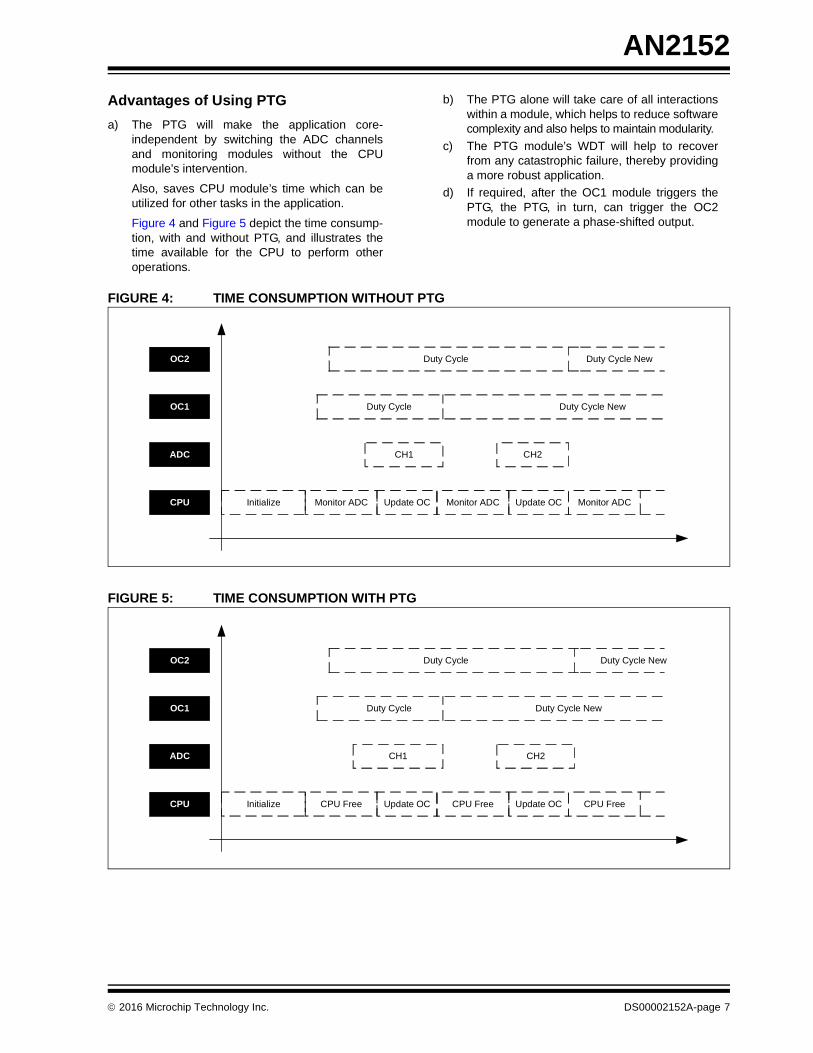
The flowchart of the application and the PTG codesequence are illustrated in Figure 6.
FIGURE 6: APPLICATION FLOWCHART AND PTG CODE SEQUENCE
PTGQPTR = 0; //Begin on _STEP0
PTGADJ = 0x2;
PTGHOLD = 0x3;
PTGL0 = 0x0;
_STEP0 = PTGWHI | 7; //Wait for input trigger from OC1
_STEP1 = PTGTRIG | 2; //Trigger OC2
_STEP2 = PTGCOPY | 13; //Copy ADC Channel number to PTGL0
_STEP3 = PTGCTRL | 14; //Change ADC Channel number
_STEP4 = PTGTRIG| 12; //Trigger ADC
_STEP5 = PTGWHI | 14; //Wait for ADC Conversion Done Trigger
_STEP6 = PTGIRQ| 1; //Generate PTG interrupt, change OC1 duty cycle
_STEP7 = PTGADD | 5; //ADD ADC Channel number to PTGL0
_STEP8 = PTGCTRL | 14; //Change ADC Channel number
_STEP9 = PTGTRIG| 12; //Trigger ADC
_STEP10 = PTGWHI | 14; //Wait for ADC Conversion Done Trigger
_STEP11 = PTGIRQ| 2; //Generate PTG interrupt, change OC2 duty
_STEP12 = PTGJMP| 2; //Repeat the process
PTGCSTbits.PTGEN = 1; //Enable PTG
PTGCSTbits.PTGSTRT = 1; //Start the sequencer
Start PTG
Wait for OC1 Trigger
No
Yes
Trigger OC2
Copy ADC Channel No. to PTGL0
Copy PTGL0 Value to ADCHS0
Trigger ADC
Wait forADC Conversion
Done TriggerNo
Yes
Generate PTG INT to Change OC1 Duty
Cycle
Modified PTGL0 Value
Copy PTGL0 Value to ADCHS0
Trigger ADC
Wait forADC Conversion
Done TriggerNo
Yes
Generate PTG INT to Change OC2 Duty
Cycle
DS00002152A-page 8 2016 Microchip Technology Inc.
AN2152
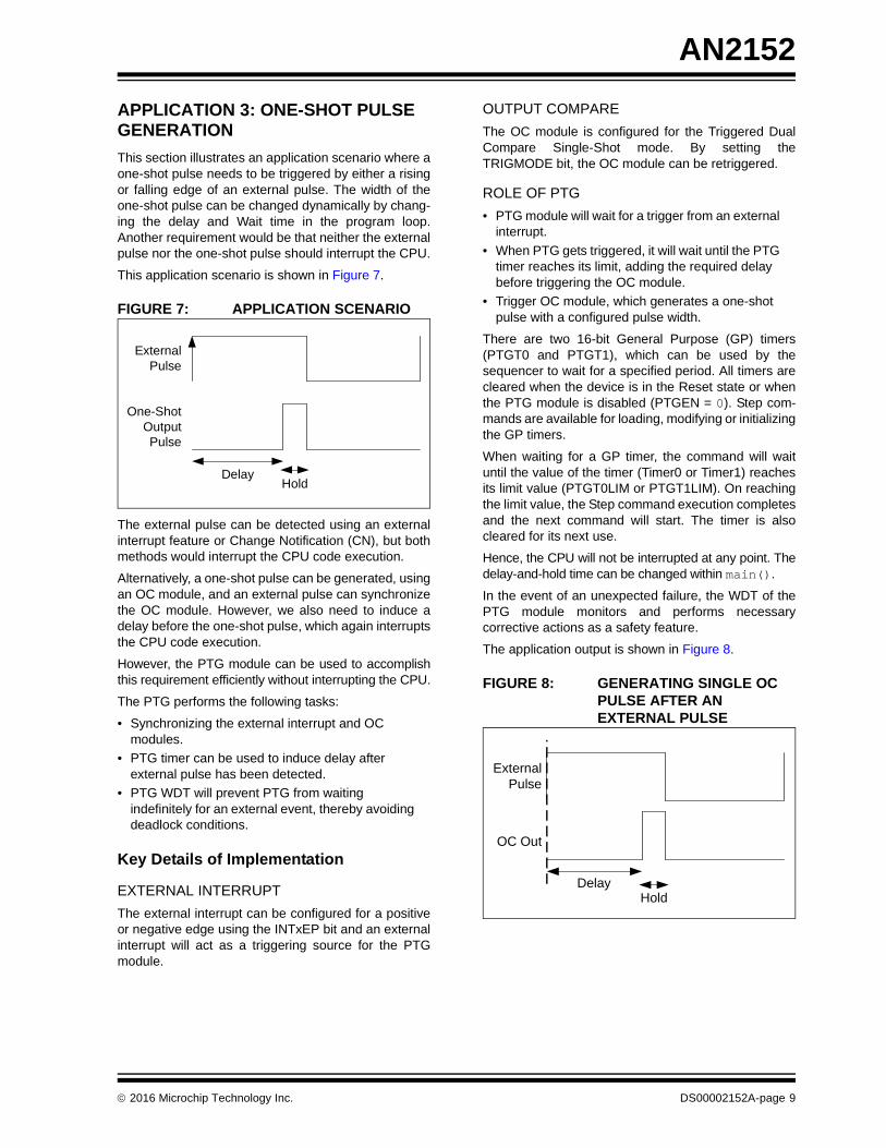
APPLICATION 3: ONE-SHOT PULSE GENERATION
This section illustrates an application scenario where aone-shot pulse needs to be triggered by either a risingor falling edge of an external pulse. The width of theone-shot pulse can be changed dynamically by chang-ing the delay and Wait time in the program loop.Another requirement would be that neither the externalpulse nor the one-shot pulse should interrupt the CPU.
This application scenario is shown in Figure 7.
FIGURE 7: APPLICATION SCENARIO
The external pulse can be detected using an externalinterrupt feature or Change Notification (CN), but bothmethods would interrupt the CPU code execution.
Alternatively, a one-shot pulse can be generated, usingan OC module, and an external pulse can synchronizethe OC module. However, we also need to induce adelay before the one-shot pulse, which again interruptsthe CPU code execution.
However, the PTG module can be used to accomplishthis requirement efficiently without interrupting the CPU.
The PTG performs the following tasks:
• Synchronizing the external interrupt and OC modules.
• PTG timer can be used to induce delay after external pulse has been detected.
• PTG WDT will prevent PTG from waiting indefinitely for an external event, thereby avoiding deadlock conditions.
Key Details of Implementation
EXTERNAL INTERRUPT
The external interrupt can be configured for a positiveor negative edge using the INTxEP bit and an externalinterrupt will act as a triggering source for the PTGmodule.
OUTPUT COMPARE
The OC module is configured for the Triggered DualCompare Single-Shot mode. By setting theTRIGMODE bit, the OC module can be retriggered.
ROLE OF PTG
• PTG module will wait for a trigger from an external interrupt.
• When PTG gets triggered, it will wait until the PTG timer reaches its limit, adding the required delay before triggering the OC module.
• Trigger OC module, which generates a one-shot pulse with a configured pulse width.
There are two 16-bit General Purpose (GP) timers(PTGT0 and PTGT1), which can be used by thesequencer to wait for a specified period. All timers arecleared when the device is in the Reset state or whenthe PTG module is disabled (PTGEN = 0). Step com-mands are available for loading, modifying or initializingthe GP timers.
When waiting for a GP timer, the command will waituntil the value of the timer (Timer0 or Timer1) reachesits limit value (PTGT0LIM or PTGT1LIM). On reachingthe limit value, the Step command execution completesand the next command will start. The timer is alsocleared for its next use.
Hence, the CPU will not be interrupted at any point. Thedelay-and-hold time can be changed within main().
In the event of an unexpected failure, the WDT of thePTG module monitors and performs necessarycorrective actions as a safety feature.
The application output is shown in Figure 8.
FIGURE 8: GENERATING SINGLE OC PULSE AFTER AN EXTERNAL PULSE
DelayHold
External Pulse
One-Shot Output Pulse
External Pulse
OC Out
DelayHold
2016 Microchip Technology Inc. DS00002152A-page 9
AN2152
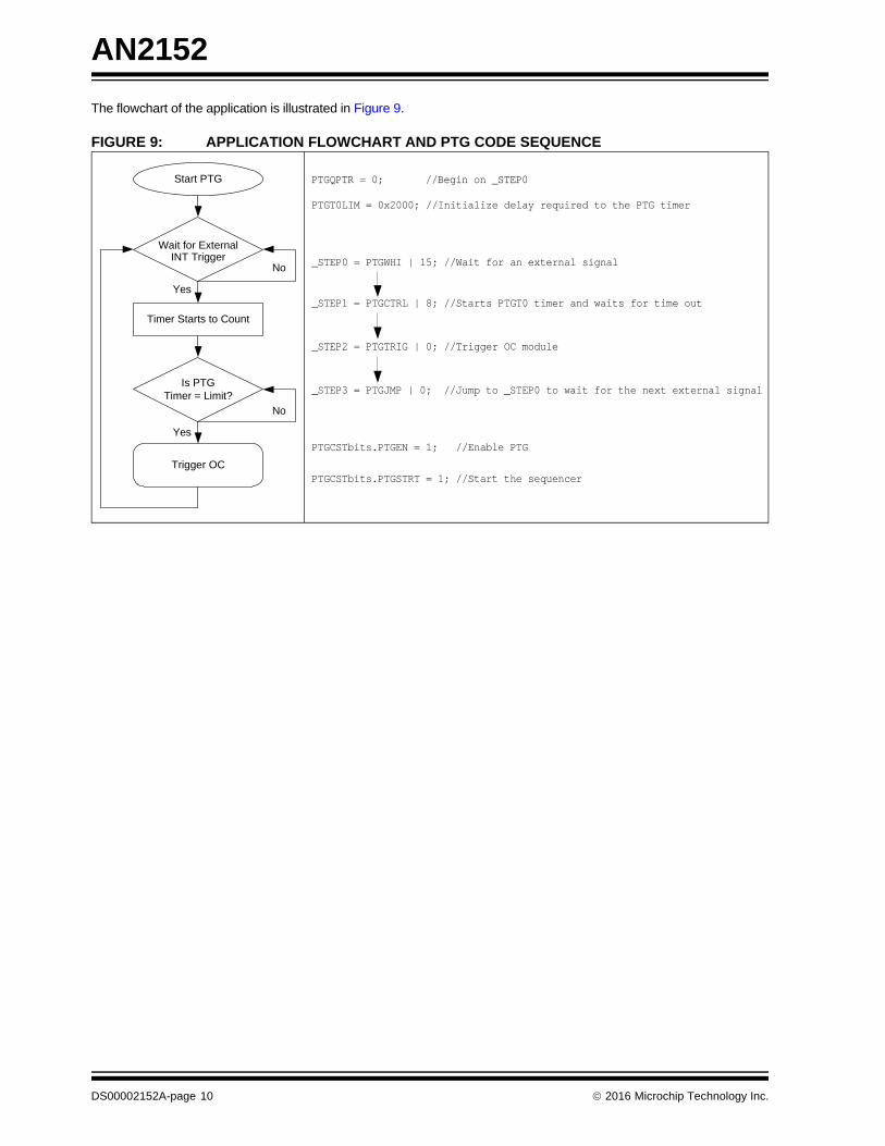
The flowchart of the application is illustrated in Figure 9.
FIGURE 9: APPLICATION FLOWCHART AND PTG CODE SEQUENCE
PTGT0LIM = 0x2000; //Initialize delay required to the PTG timer
_STEP0 = PTGWHI | 15; //Wait for an external signal
_STEP1 = PTGCTRL | 8; //Starts PTGT0 timer and waits for time out
_STEP2 = PTGTRIG | 0; //Trigger OC module
_STEP3 = PTGJMP | 0; //Jump to _STEP0 to wait for the next external signal
PTGQPTR = 0; //Begin on _STEP0
PTGCSTbits.PTGEN = 1; //Enable PTG
PTGCSTbits.PTGSTRT = 1; //Start the sequencer
Start PTG
Wait for External INT Trigger
No
Timer Starts to Count
Is PTG Timer = Limit?
No
Trigger OC
Yes
Yes
DS00002152A-page 10 2016 Microchip Technology Inc.
AN2152
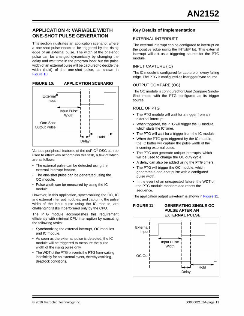
APPLICATION 4: VARIABLE WIDTH ONE-SHOT PULSE GENERATION
This section illustrates an application scenario, wherea one-shot pulse needs to be triggered by the risingedge of an external pulse. The width of the one-shotpulse can be changed dynamically by changing thedelay and wait time in the program loop; but the pulsewidth of an external pulse will be captured to decide thewidth (hold) of the one-shot pulse, as shown inFigure 10.
FIGURE 10: APPLICATION SCENARIO
Various peripheral features of the dsPIC® DSC can beused to effectively accomplish this task, a few of whichare as follows:
• The external pulse can be detected using the external interrupt feature.
• The one-shot pulse can be generated using the OC module.
• Pulse width can be measured by using the IC module.
However, in this application, synchronizing the OC, ICand external interrupt modules, and capturing the pulsewidth of the input pulse using the IC module, arechallenging tasks if performed only by the CPU.
The PTG module accomplishes this requirementefficiently with minimal CPU interruption by executingthe following tasks:
• Synchronizing the external interrupt, OC modules and IC module.
• As soon as the external pulse is detected, the IC module will be triggered to measure the pulse width of the rising pulse only.
• The WDT of the PTG prevents the PTG from waiting indefinitely for an external event, thereby avoiding deadlock conditions.
Key Details of Implementation
EXTERNAL INTERRUPT
The external interrupt can be configured to interrupt onthe positive edge using the INTxEP bit. This externalinterrupt will act as a triggering source for the PTGmodule.
INPUT CAPTURE (IC)
The IC module is configured for capture on every fallingedge. The PTG is configured as its trigger/sync source.
OUTPUT COMPARE (OC)
The OC module is configured for Dual Compare Single-Shot mode with the PTG configured as its triggersource.
ROLE OF PTG
• The PTG module will wait for a trigger from an external interrupt.
• When triggered, the PTG will trigger the IC module, which starts the IC timer.
• The PTG will wait for a trigger from the IC module.
• When the PTG gets triggered by the IC module, the IC buffer will capture the pulse width of the incoming external pulse.
• The PTG can generate unique interrupts, which will be used to change the OC duty cycle.
• A delay can also be added using the PTG timers.
• The PTG will trigger the OC module, which generates a one-shot pulse with a configured pulse width.
• In the event of an unexpected failure, the WDT of the PTG module monitors and resets the sequence.
The application output waveform is shown in Figure 11.
FIGURE 11: GENERATING SINGLE OC PULSE AFTER AN EXTERNAL PULSE
Input Pulse Width
Hold
External Input
One-Shot Output Pulse
Delay
External Input
OC Out
Hold
Input Pulse Width
Delay
2016 Microchip Technology Inc. DS00002152A-page 11
AN2152
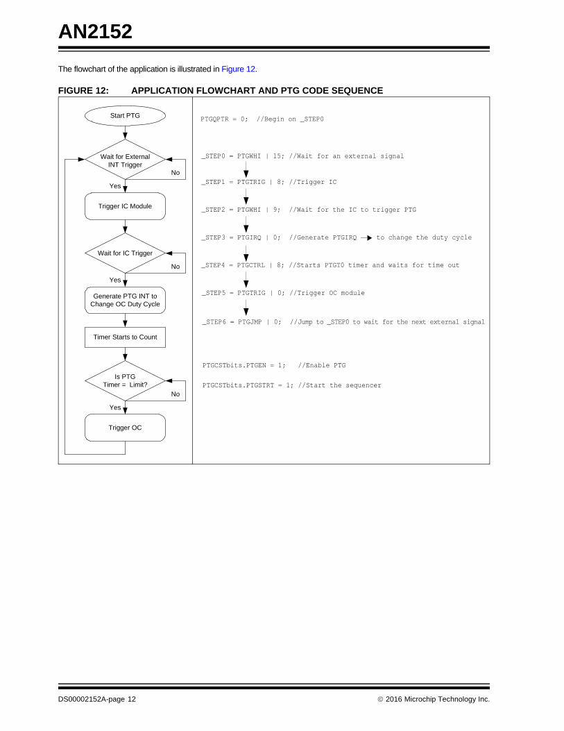
The flowchart of the application is illustrated in Figure 12.
FIGURE 12: APPLICATION FLOWCHART AND PTG CODE SEQUENCE
_STEP0 = PTGWHI | 15; //Wait for an external signal
_STEP1 = PTGTRIG | 8; //Trigger IC
_STEP2 = PTGWHI | 9; //Wait for the IC to trigger PTG
_STEP3 = PTGIRQ | 0; //Generate PTGIRQ to change the duty cycle
_STEP5 = PTGTRIG | 0; //Trigger OC module
_STEP4 = PTGCTRL | 8; //Starts PTGT0 timer and waits for time out
_STEP6 = PTGJMP | 0; //Jump to _STEP0 to wait for the next external signal
PTGQPTR = 0; //Begin on _STEP0
PTGCSTbits.PTGEN = 1; //Enable PTG
PTGCSTbits.PTGSTRT = 1; //Start the sequencer
Start PTG
Wait for External INT Trigger
No
Trigger IC Module
Is PTGTimer = Limit?
No
Trigger OC
Yes
Yes
Timer Starts to Count
Wait for IC Trigger
No
Yes
Generate PTG INT to Change OC Duty Cycle
DS00002152A-page 12 2016 Microchip Technology Inc.
AN2152
APPLICATION 5: VARIABLE FREQUENCY WAVEFORM GENERATION
This application illustrates how the PTG can be used togenerate a variable frequency signal generator.
The OC modules, along with DMA, can be used togenerate variable frequency signals.
However, the PTG can provide an additional mechanismto generate a variable frequency signal, as describedbelow.
The solution would use the following PTG features:
• The PTG has its own timer, which runs independently of the CPU.
• The PTG has ADD and COPY commands, which can write to the Timer Limit register.
• The PTG can generate its own interrupt.
The control techniques used in the application involvethe following steps:
• Configuring the PTG with the timer limit value, as well as the adjust value, which will be added to the Timer Limit register.
• Generating the PTG ISR, where a general purpose I/O pin is toggled.
• Waiting for the timer to reach its limit value.- On reaching the limit value, the Step
command execution completes, and in the next command, adds the PTGADJ value to the Timer Limit register.
- The CPU will be interrupted only while toggling the I/O pin.
There are two 16-bit General Purpose timers (PTGT0and PTGT1), which can be used by the sequencer towait for a specified period. All timers are cleared whenthe device is in the Reset state or when the PTGmodule is disabled (PTGEN = 0). Step commands areavailable for loading, modifying or initializing the GPtimers.
When waiting for the GP timer, the command will waituntil the value of the timer (Timer0 or Timer1) reachesits limit value (PTGT0LIM or PTGT1LIM). On reachingthe limit value, the Step command execution completesand the execution of the next command will start. Thetimer is also cleared for its subsequent use.
The timer limit value can be modified using the PTGADDor PTGCOPY commands. The PTGADD command willadd the PTGADJ register contents to the PTGCxLIMregister. The PTGCOPY command will copy thePTGHOLD register contents to the PTGCxLIM register.
The application output is as shown in Figure 13.
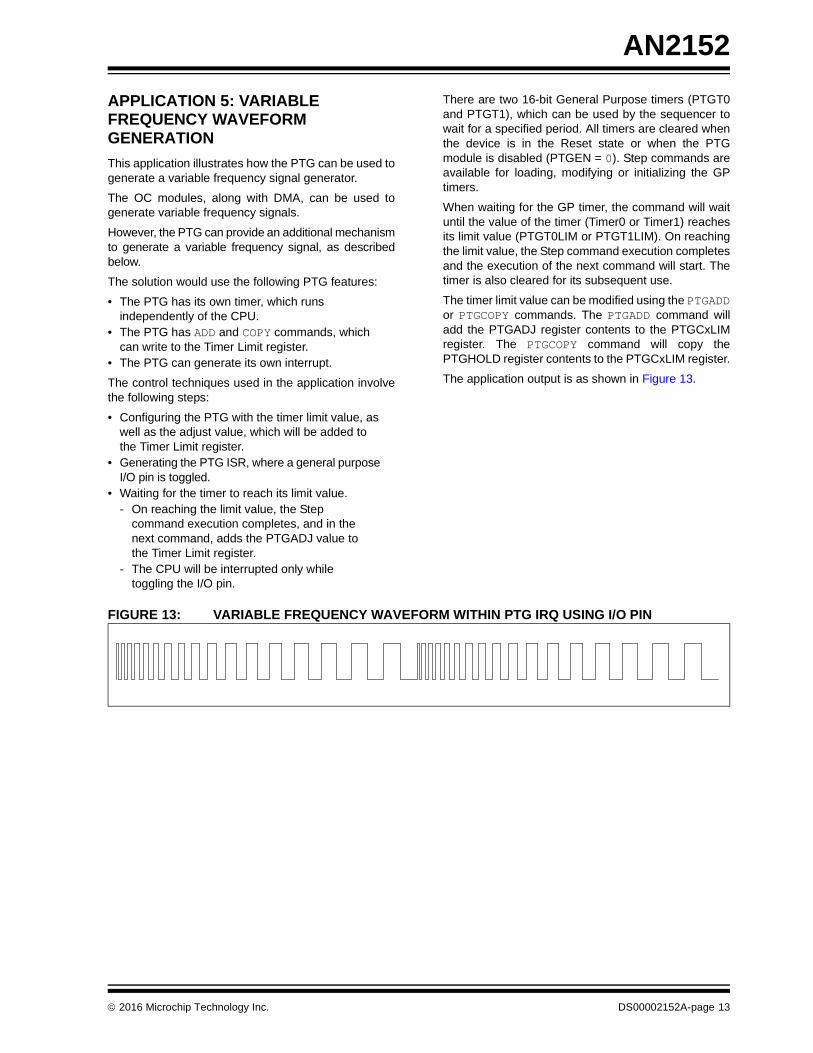
FIGURE 13: VARIABLE FREQUENCY WAVEFORM WITHIN PTG IRQ USING I/O PIN
2016 Microchip Technology Inc. DS00002152A-page 13
AN2152
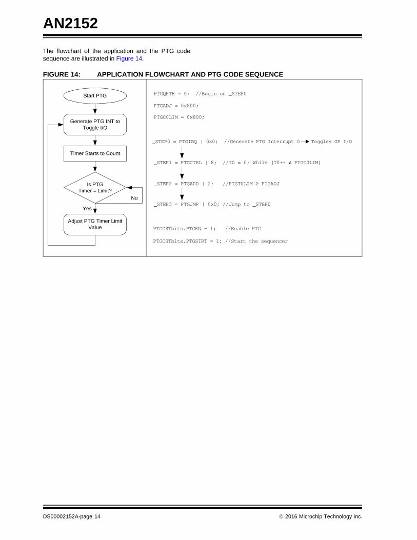
The flowchart of the application and the PTG codesequence are illustrated in Figure 14.
FIGURE 14: APPLICATION FLOWCHART AND PTG CODE SEQUENCE
PTGQPTR = 0; //Begin on _STEP0
PTGADJ = 0x800;
PTGC0LIM = 0x800;
_STEP1 = PTGCTRL | 8; //T0 = 0; While (T0++ PTGT0LIM)
_STEP2 = PTGADD | 2; //PTGT0LIM PTGADJ
_STEP3 = PTGJMP | 0x0; //Jump to _STEP0
PTGCSTbits.PTGEN = 1; //Enable PTG
PTGCSTbits.PTGSTRT = 1; //Start the sequencer
_STEP0 = PTGIRQ | 0x0; //Generate PTG Interrupt 0 Toggles GP I/O
Start PTG
Timer Starts to Count
Is PTG Timer = Limit?
No
Adjust PTG Timer Limit Value
Yes
Generate PTG INT to Toggle I/O
DS00002152A-page 14 2016 Microchip Technology Inc.
AN2152
APPLICATION 6: CONSTANT FREQUENCY WAVEFORM GENERATION
This application illustrates how the PTG module can beused to generate a constant frequency signal, whichcan also act as a clock source.
The solution would use the following features of thePTG module’s features:
• PTG can trigger a comparator, which acts as a mask input select
• The PTG module’s trigger pulse width can be varied
• PTG has its own timer
The control techniques used in the application involvethe following steps:
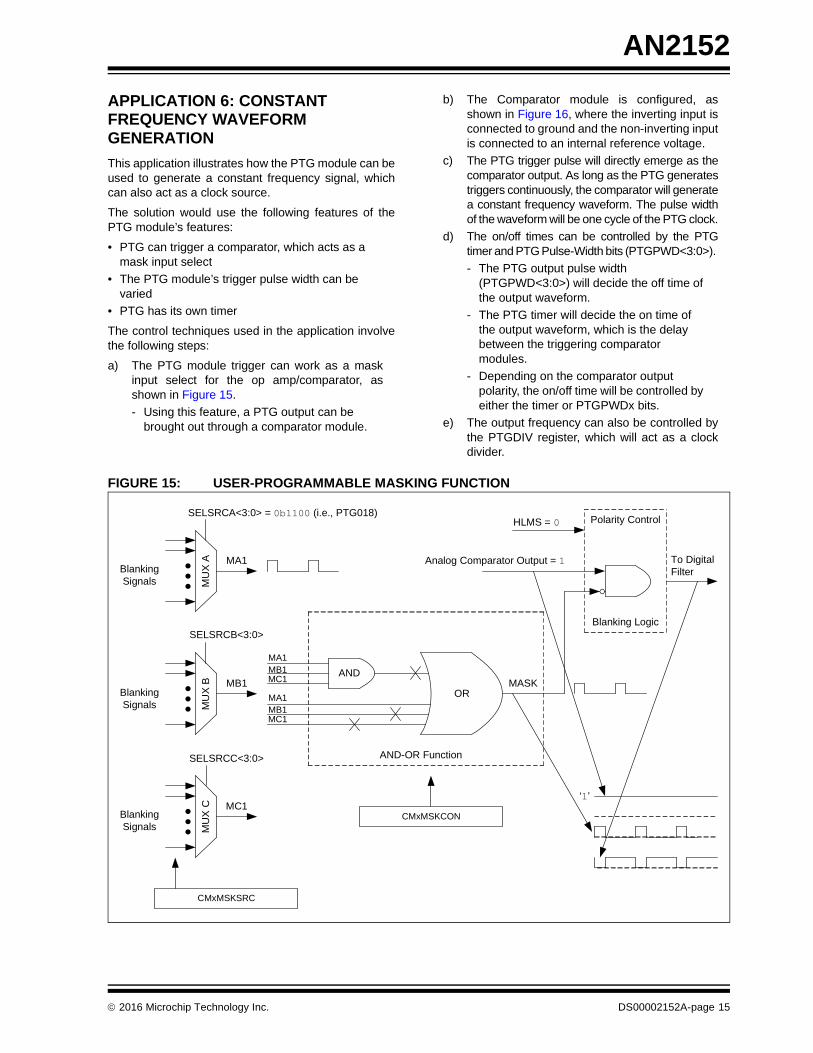
a) The PTG module trigger can work as a maskinput select for the op amp/comparator, asshown in Figure 15.
- Using this feature, a PTG output can be brought out through a comparator module.
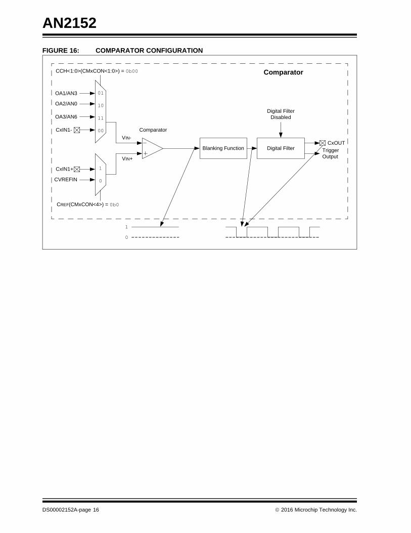
b) The Comparator module is configured, asshown in Figure 16, where the inverting input isconnected to ground and the non-inverting inputis connected to an internal reference voltage.
c) The PTG trigger pulse will directly emerge as thecomparator output. As long as the PTG generatestriggers continuously, the comparator will generatea constant frequency waveform. The pulse widthof the waveform will be one cycle of the PTG clock.
d) The on/off times can be controlled by the PTGtimer and PTG Pulse-Width bits (PTGPWD<3:0>).
- The PTG output pulse width (PTGPWD<3:0>) will decide the off time of the output waveform.
- The PTG timer will decide the on time of the output waveform, which is the delay between the triggering comparator modules.
- Depending on the comparator output polarity, the on/off time will be controlled by either the timer or PTGPWDx bits.
e) The output frequency can also be controlled bythe PTGDIV register, which will act as a clockdivider.
FIGURE 15: USER-PROGRAMMABLE MASKING FUNCTION
To Digital Filter
MU
X A
MU
X B
MU
X C
AND
ORMASK
MA1
MB1
MC1
MA1MB1MC1
MA1MB1MC1
CMxMSKSRC
CMxMSKCON
SELSRCA<3:0> = 0b1100 (i.e., PTG018)
SELSRCB<3:0>
SELSRCC<3:0>
Blanking Signals
Blanking Signals
Blanking Signals
Analog Comparator Output = 1
Polarity Control
Blanking Logic
AND-OR Function
HLMS = 0
‘1’
2016 Microchip Technology Inc. DS00002152A-page 15
AN2152
FIGURE 16: COMPARATOR CONFIGURATION
Blanking Function
01
10
11
00
1
0
Comparator
VIN+
VIN-
Digital Filter
CREF(CMxCON<4>) = 0b0
CCH<1:0>(CMxCON<1:0>) = 0b00
OA1/AN3
OA2/AN0
OA3/AN6
CxIN1-
CxIN1+
CVREFIN
1
0
Digital Filter Disabled
Comparator
CxOUT
Trigger Output
DS00002152A-page 16 2016 Microchip Technology Inc.
AN2152
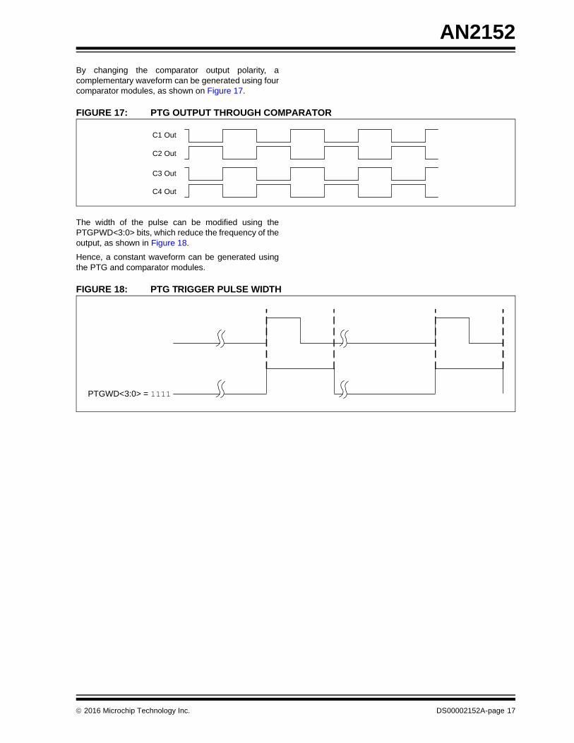
By changing the comparator output polarity, acomplementary waveform can be generated using fourcomparator modules, as shown on Figure 17.
FIGURE 17: PTG OUTPUT THROUGH COMPARATOR
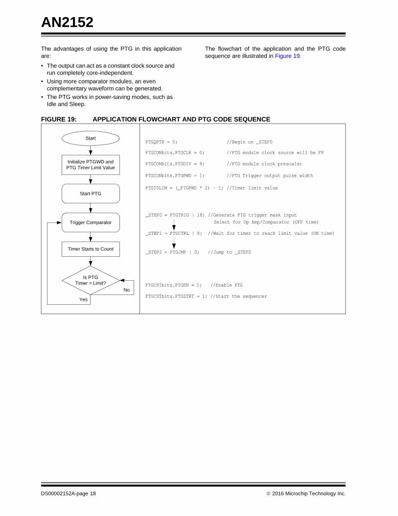
The width of the pulse can be modified using thePTGPWD<3:0> bits, which reduce the frequency of theoutput, as shown in Figure 18.
Hence, a constant waveform can be generated usingthe PTG and comparator modules.
FIGURE 18: PTG TRIGGER PULSE WIDTH
C1 Out
C2 Out
C3 Out
C4 Out
PTGWD<3:0> = 1111
2016 Microchip Technology Inc. DS00002152A-page 17
AN2152
The advantages of using the PTG in this applicationare:
• The output can act as a constant clock source and run completely core-independent.
• Using more comparator modules, an even complementary waveform can be generated.
• The PTG works in power-saving modes, such as Idle and Sleep.
The flowchart of the application and the PTG codesequence are illustrated in Figure 19.
FIGURE 19: APPLICATION FLOWCHART AND PTG CODE SEQUENCE
PTGQPTR = 0; //Begin on _STEP0
PTGCONbits.PTGCLK = 0; //PTG module clock source will be FP
PTGCONbits.PTGDIV = 9; //PTG module clock prescaler
PTGCONbits.PTGPWD = 1; //PTG Trigger output pulse width
PTGT0LIM = (_PTGPWD * 2) - 1; //Timer limit value
_STEP0 = PTGTRIG | 18; //Generate PTG trigger mask input
_STEP1 = PTGCTRL | 8; //Wait for timer to reach limit value (ON time)
_STEP2 = PTGJMP | 0; //Jump to _STEP0
PTGCSTbits.PTGEN = 1; //Enable PTG
PTGCSTbits.PTGSTRT = 1; //Start the sequencer
Select for Op Amp/Comparator (OFF time)
Start
Timer Starts to Count
Is PTG Timer = Limit?
No
Start PTG
Yes
Trigger Comparator
Initialize PTGWD and PTG Timer Limit Value
DS00002152A-page 18 2016 Microchip Technology Inc.
AN2152
APPLICATION 7: ADC MODULE CONTROL
The PTG module has many options to control the ADC,which is very helpful for synchronizing the ADC andother modules, as the PTG enables a large number ofperipherals to trigger an ADC conversion. The PTGalso enables the ADC trigger sources to be changeddynamically.
The PTG makes the process of controlling the ADCmodule core-independent, as the ADC can directlytrigger the PTG after the conversion is done. If it werenot for this feature, the ADC DONE bit would havebeen polled by the CPU or the ADC interrupt wouldhave indicated the end of conversion.
The PTG can also change the ADC channel with itsStrobe command. The strobe output of the PTGmodule can be used to write to the AD1CHS0 register(refer to Table 2).
TABLE 2: ADC CHANNEL MODIFICATION OPTIONS
Command Options Description
PTGCTRL 0x1100 Writes the PTGL0 register contents to the AD1CHS0 register
PTGADD and PTGCOPY — Modifies the PTGL0 register
PTGCTRL 0x1100 Writes the PTGC0 register contents to the AD1CHS0 register
PTGCTRL 0x1101 Writes the PTGC1 register contents to the AD1CHS0 register
2016 Microchip Technology Inc. DS00002152A-page 19
AN2152
These features are also used in other applications, forexample:
• In the “Application 1: Integrated PFC and Motor Control” section, the PWM and PFC channels are changed within the PTG ISR.
• In the “Application 2: Lighting Control” section, the PTGL0 with the PTGADD and PTGHOLD com-mands were used to switch the channel to be scanned without the CPU module’s intervention.
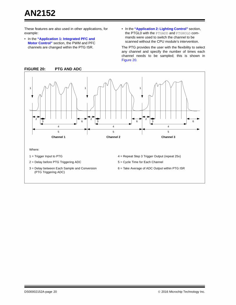
The PTG provides the user with the flexibility to selectany channel and specify the number of times eachchannel needs to be sampled; this is shown inFigure 20.
FIGURE 20: PTG AND ADC
Where:
1 = Trigger Input to PTG
2 = Delay before PTG Triggering ADC
3 = Delay between Each Sample and Conversion
4 = Repeat Step 3 Trigger Output (repeat 25x)
5 = Cycle Time for Each Channel
6 = Take Average of ADC Output within PTG ISR
(PTG Triggering ADC)
Channel 1 Channel 2 Channel 3
1
23
4
5
6
1 1
23
4
5
62
3
4
5
6
DS00002152A-page 20 2016 Microchip Technology Inc.
AN2152
Using this flexibility, the PTG can be used to automatethe ADC sampling process using following steps:
a) The PTG is configured for an appropriate timerlimit value to give enough time between triggers.
b) The ADC is configured with the PTG as a triggersource.
c) The PTG counter will be useful in repeating asmany times as the ADC needs to be triggered.
d) The PTG ISR will take the average of the ADCoutputs and also change the ADC channels byusing the Strobe command.
The flowchart of the application and PTG codesequence are illustrated in Figure 21.
FIGURE 21: APPLICATION FLOWCHART AND PTG CODE SEQUENCE
_STEP0 = PTGWHI|15; //Waiting for input trigger from EXT INT
_STEP1 = PTGSTRB|14; //Write channel to ADCHS0
_STEP2 = PTGCTRL|8; //Wait for timer to reach limit
_STEP3 = PTGTRIG|12; //Trigger ADC
_STEP4 = PTGWHI|14; //Wait for ADC Conversion Done trigger
_STEP5 = PTGJMPC0|3; //Retrigger ADC
_STEP6 = PTGIRQ|1; //Generate PTG interrupt; Average of ADC output
_STEP7 = PTGADD|5; //Add ADC channel number to PTGL0, New channel
_STEP8 = PTGJMP|1; //Change ADC channel number
PTGQPTR = 0; //Begin on _STEP0
PTGCSTbits.PTGEN = 1; //Enable PTG
PTGCSTbits.PTGSTRT = 1; //Start the sequencer
Is Counter = Limit?
No
Yes
Start
Wait forADC Conversion
Done TriggerNo
Change ADC Channel
Yes
Trigger ADC
Wait for EXT INT
No
Yes
Is PTG Timer = Limit?
No
Yes
Generate PTG INT to Take Average of Samples
Modify ADC Channel
2016 Microchip Technology Inc. DS00002152A-page 21
AN2152
SUMMARY
The PTG module in Microchip’s DSC devices allowsusers to design complex application sequences withflexibility. A PTG allows various modules to interactwith each other with minimum or no CPU interruptionand also enhances the capabilities of the existingperipherals, thus expanding the horizon of applicationsa peripheral can accomplish.
With the PTG module, the applications can have fasterresponse time and incur minimal software burden. ThePTG also provides additional safety to the applicationswith built-in functions.
There are a wide range of applications that can beimplemented using PTG, of which only a few are dis-cussed in this document. Microchip encourages usersto explore other possibilities of using PTG.
REFERENCES
1. Peripheral Trigger Generator (PTG) in the “dsPIC33/PIC24 Family Reference Manual”
http://ww1.microchip.com/downloads/en/DeviceDoc/DS-70669A.pdf
2. Sensorless Field Oriented Control (FOC) for a Permanent Magnet Synchronous Motor (PMSM) Using a PLL Estimator and Field Weakening (FW),
http://ww1.microchip.com/downloads/en/AppNotes/01292A.pdf
3. Analog-to-Digital Converter (ADC) in the “dsPIC33/PIC24 Family Reference Manual”
http://ww1.microchip.com/downloads/en/DeviceDoc/70621c.pdf
DS00002152A-page 22 2016 Microchip Technology Inc.
Note the following details of the code protection feature on Microchip devices:
• Microchip products meet the specification contained in their particular Microchip Data Sheet.
• Microchip believes that its family of products is one of the most secure families of its kind on the market today, when used in the intended manner and under normal conditions.
• There are dishonest and possibly illegal methods used to breach the code protection feature. All of these methods, to our knowledge, require using the Microchip products in a manner outside the operating specifications contained in Microchip’s Data Sheets. Most likely, the person doing so is engaged in theft of intellectual property.
• Microchip is willing to work with the customer who is concerned about the integrity of their code.
• Neither Microchip nor any other semiconductor manufacturer can guarantee the security of their code. Code protection does not mean that we are guaranteeing the product as “unbreakable.”
Code protection is constantly evolving. We at Microchip are committed to continuously improving the code protection features of ourproducts. Attempts to break Microchip’s code protection feature may be a violation of the Digital Millennium Copyright Act. If such actsallow unauthorized access to your software or other copyrighted work, you may have a right to sue for relief under that Act.
Information contained in this publication regarding deviceapplications and the like is provided only for your convenienceand may be superseded by updates. It is your responsibility toensure that your application meets with your specifications.MICROCHIP MAKES NO REPRESENTATIONS ORWARRANTIES OF ANY KIND WHETHER EXPRESS ORIMPLIED, WRITTEN OR ORAL, STATUTORY OROTHERWISE, RELATED TO THE INFORMATION,INCLUDING BUT NOT LIMITED TO ITS CONDITION,QUALITY, PERFORMANCE, MERCHANTABILITY ORFITNESS FOR PURPOSE. Microchip disclaims all liabilityarising from this information and its use. Use of Microchipdevices in life support and/or safety applications is entirely atthe buyer’s risk, and the buyer agrees to defend, indemnify andhold harmless Microchip from any and all damages, claims,suits, or expenses resulting from such use. No licenses areconveyed, implicitly or otherwise, under any Microchipintellectual property rights unless otherwise stated.
2016 Microchip Technology Inc.
Microchip received ISO/TS-16949:2009 certification for its worldwide headquarters, design and wafer fabrication facilities in Chandler and Tempe, Arizona; Gresham, Oregon and design centers in California and India. The Company’s quality system processes and procedures are for its PIC® MCUs and dsPIC® DSCs, KEELOQ® code hopping devices, Serial EEPROMs, microperipherals, nonvolatile memory and analog products. In addition, Microchip’s quality system for the design and manufacture of development systems is ISO 9001:2000 certified.
QUALITY MANAGEMENT SYSTEM CERTIFIED BY DNV
== ISO/TS 16949 ==
Trademarks
The Microchip name and logo, the Microchip logo, AnyRate, dsPIC, FlashFlex, flexPWR, Heldo, JukeBlox, KeeLoq, KeeLoq logo, Kleer, LANCheck, LINK MD, MediaLB, MOST, MOST logo, MPLAB, OptoLyzer, PIC, PICSTART, PIC32 logo, RightTouch, SpyNIC, SST, SST Logo, SuperFlash and UNI/O are registered trademarks of Microchip Technology Incorporated in the U.S.A. and other countries.
ClockWorks, The Embedded Control Solutions Company, ETHERSYNCH, Hyper Speed Control, HyperLight Load, IntelliMOS, mTouch, Precision Edge, and QUIET-WIRE are registered trademarks of Microchip Technology Incorporated in the U.S.A.
Analog-for-the-Digital Age, Any Capacitor, AnyIn, AnyOut, BodyCom, chipKIT, chipKIT logo, CodeGuard, dsPICDEM, dsPICDEM.net, Dynamic Average Matching, DAM, ECAN, EtherGREEN, In-Circuit Serial Programming, ICSP, Inter-Chip Connectivity, JitterBlocker, KleerNet, KleerNet logo, MiWi, motorBench, MPASM, MPF, MPLAB Certified logo, MPLIB, MPLINK, MultiTRAK, NetDetach, Omniscient Code Generation, PICDEM, PICDEM.net, PICkit, PICtail, PureSilicon, RightTouch logo, REAL ICE, Ripple Blocker, Serial Quad I/O, SQI, SuperSwitcher, SuperSwitcher II, Total Endurance, TSHARC, USBCheck, VariSense, ViewSpan, WiperLock, Wireless DNA, and ZENA are trademarks of Microchip Technology Incorporated in the U.S.A. and other countries.
SQTP is a service mark of Microchip Technology Incorporated in the U.S.A.
Silicon Storage Technology is a registered trademark of Microchip Technology Inc. in other countries.
GestIC is a registered trademarks of Microchip Technology Germany II GmbH & Co. KG, a subsidiary of Microchip Technology Inc., in other countries.
All other trademarks mentioned herein are property of their respective companies.
© 2016, Microchip Technology Incorporated, Printed in the U.S.A., All Rights Reserved.
ISBN: 978-1-5224-0651-8
DS00002152A-page 23

DS00002152A-page 24 2016 Microchip Technology Inc.
AMERICASCorporate Office2355 West Chandler Blvd.Chandler, AZ 85224-6199Tel: 480-792-7200 Fax: 480-792-7277Technical Support: http://www.microchip.com/supportWeb Address: www.microchip.com
AtlantaDuluth, GA Tel: 678-957-9614 Fax: 678-957-1455
Austin, TXTel: 512-257-3370
BostonWestborough, MA Tel: 774-760-0087 Fax: 774-760-0088
ChicagoItasca, IL Tel: 630-285-0071 Fax: 630-285-0075
ClevelandIndependence, OH Tel: 216-447-0464 Fax: 216-447-0643
DallasAddison, TX Tel: 972-818-7423 Fax: 972-818-2924
DetroitNovi, MI Tel: 248-848-4000
Houston, TX Tel: 281-894-5983
IndianapolisNoblesville, IN Tel: 317-773-8323Fax: 317-773-5453
Los AngelesMission Viejo, CA Tel: 949-462-9523 Fax: 949-462-9608
New York, NY Tel: 631-435-6000
San Jose, CA Tel: 408-735-9110
Canada - TorontoTel: 905-673-0699 Fax: 905-673-6509
ASIA/PACIFICAsia Pacific OfficeSuites 3707-14, 37th FloorTower 6, The GatewayHarbour City, Kowloon
Hong KongTel: 852-2943-5100Fax: 852-2401-3431
Australia - SydneyTel: 61-2-9868-6733Fax: 61-2-9868-6755
China - BeijingTel: 86-10-8569-7000 Fax: 86-10-8528-2104
China - ChengduTel: 86-28-8665-5511Fax: 86-28-8665-7889
China - ChongqingTel: 86-23-8980-9588Fax: 86-23-8980-9500
China - DongguanTel: 86-769-8702-9880
China - HangzhouTel: 86-571-8792-8115 Fax: 86-571-8792-8116
China - Hong Kong SARTel: 852-2943-5100 Fax: 852-2401-3431
China - NanjingTel: 86-25-8473-2460Fax: 86-25-8473-2470
China - QingdaoTel: 86-532-8502-7355Fax: 86-532-8502-7205
China - ShanghaiTel: 86-21-5407-5533 Fax: 86-21-5407-5066
China - ShenyangTel: 86-24-2334-2829Fax: 86-24-2334-2393
China - ShenzhenTel: 86-755-8864-2200 Fax: 86-755-8203-1760
China - WuhanTel: 86-27-5980-5300Fax: 86-27-5980-5118
China - XianTel: 86-29-8833-7252Fax: 86-29-8833-7256
ASIA/PACIFICChina - XiamenTel: 86-592-2388138 Fax: 86-592-2388130
China - ZhuhaiTel: 86-756-3210040 Fax: 86-756-3210049
India - BangaloreTel: 91-80-3090-4444 Fax: 91-80-3090-4123
India - New DelhiTel: 91-11-4160-8631Fax: 91-11-4160-8632
India - PuneTel: 91-20-3019-1500
Japan - OsakaTel: 81-6-6152-7160 Fax: 81-6-6152-9310
Japan - TokyoTel: 81-3-6880- 3770 Fax: 81-3-6880-3771
Korea - DaeguTel: 82-53-744-4301Fax: 82-53-744-4302
Korea - SeoulTel: 82-2-554-7200Fax: 82-2-558-5932 or 82-2-558-5934
Malaysia - Kuala LumpurTel: 60-3-6201-9857Fax: 60-3-6201-9859
Malaysia - PenangTel: 60-4-227-8870Fax: 60-4-227-4068
Philippines - ManilaTel: 63-2-634-9065Fax: 63-2-634-9069
SingaporeTel: 65-6334-8870Fax: 65-6334-8850
Taiwan - Hsin ChuTel: 886-3-5778-366Fax: 886-3-5770-955
Taiwan - KaohsiungTel: 886-7-213-7828
Taiwan - TaipeiTel: 886-2-2508-8600 Fax: 886-2-2508-0102
Thailand - BangkokTel: 66-2-694-1351Fax: 66-2-694-1350
EUROPEAustria - WelsTel: 43-7242-2244-39Fax: 43-7242-2244-393
Denmark - CopenhagenTel: 45-4450-2828 Fax: 45-4485-2829
France - ParisTel: 33-1-69-53-63-20 Fax: 33-1-69-30-90-79
Germany - DusseldorfTel: 49-2129-3766400
Germany - KarlsruheTel: 49-721-625370
Germany - MunichTel: 49-89-627-144-0 Fax: 49-89-627-144-44
Italy - Milan Tel: 39-0331-742611 Fax: 39-0331-466781
Italy - VeniceTel: 39-049-7625286
Netherlands - DrunenTel: 31-416-690399 Fax: 31-416-690340
Poland - WarsawTel: 48-22-3325737
Spain - MadridTel: 34-91-708-08-90Fax: 34-91-708-08-91
Sweden - StockholmTel: 46-8-5090-4654
UK - WokinghamTel: 44-118-921-5800Fax: 44-118-921-5820
Worldwide Sales and Service
07/14/15


![Atmel AT03030: QMatrix Touchpad – 2D Position …ww1.microchip.com/downloads/en/AppNotes/Atmel-42202...Atmel AT03030: QMatrix Touchpad – 2D Position Tracking [APPLICATION NOTE]](https://img.pdfslide.us/doc/110x75/5e82bfb366844315cb3c3385/atmel-at03030-qmatrix-touchpad-a-2d-position-ww1-atmel-at03030-qmatrix.jpg)