Embed Size (px)
Citation preview
JLMN-Journal of Laser Micro/Nanoengineering Vol. 6, No. 3, 2011
260
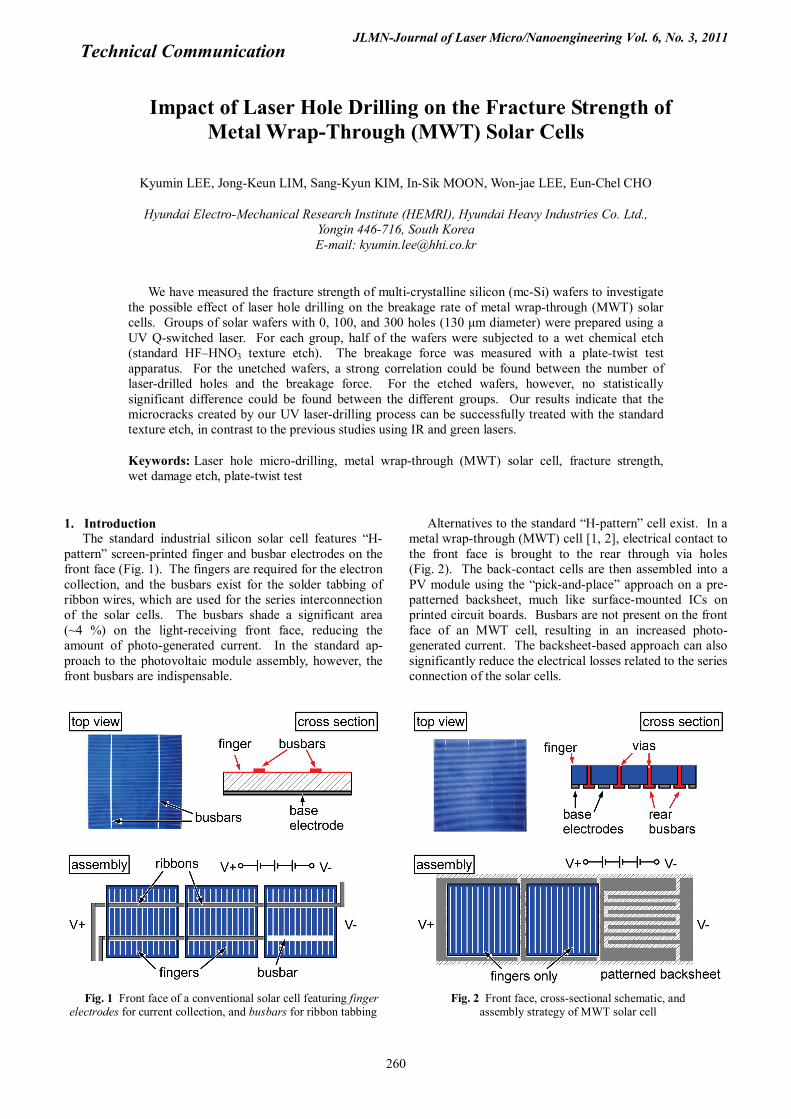
Impact of Laser Hole Drilling on the Fracture Strength of Metal Wrap-Through (MWT) Solar Cells
Kyumin LEE, Jong-Keun LIM, Sang-Kyun KIM, In-Sik MOON, Won-jae LEE, Eun-Chel CHO
Hyundai Electro-Mechanical Research Institute (HEMRI), Hyundai Heavy Industries Co. Ltd., Yongin 446-716, South Korea E-mail: [email protected]
We have measured the fracture strength of multi-crystalline silicon (mc-Si) wafers to investigate the possible effect of laser hole drilling on the breakage rate of metal wrap-through (MWT) solar cells. Groups of solar wafers with 0, 100, and 300 holes (130 μm diameter) were prepared using a UV Q-switched laser. For each group, half of the wafers were subjected to a wet chemical etch (standard HF–HNO3 texture etch). The breakage force was measured with a plate-twist test apparatus. For the unetched wafers, a strong correlation could be found between the number of laser-drilled holes and the breakage force. For the etched wafers, however, no statistically significant difference could be found between the different groups. Our results indicate that the microcracks created by our UV laser-drilling process can be successfully treated with the standard texture etch, in contrast to the previous studies using IR and green lasers.
Keywords: Laser hole micro-drilling, metal wrap-through (MWT) solar cell, fracture strength, wet damage etch, plate-twist test
1. Introduction The standard industrial silicon solar cell features “H-
pattern” screen-printed finger and busbar electrodes on the front face (Fig. 1). The fingers are required for the electron collection, and the busbars exist for the solder tabbing of ribbon wires, which are used for the series interconnection of the solar cells. The busbars shade a significant area (~4 %) on the light-receiving front face, reducing the amount of photo-generated current. In the standard ap-proach to the photovoltaic module assembly, however, the front busbars are indispensable.
Fig. 1 Front face of a conventional solar cell featuring finger
electrodes for current collection, and busbars for ribbon tabbing
Alternatives to the standard “H-pattern” cell exist. In a metal wrap-through (MWT) cell [1, 2], electrical contact to the front face is brought to the rear through via holes (Fig. 2). The back-contact cells are then assembled into a PV module using the “pick-and-place” approach on a pre-patterned backsheet, much like surface-mounted ICs on printed circuit boards. Busbars are not present on the front face of an MWT cell, resulting in an increased photo-generated current. The backsheet-based approach can also significantly reduce the electrical losses related to the series connection of the solar cells.
Fig. 2 Front face, cross-sectional schematic, and
assembly strategy of MWT solar cell
Technical Communication
JLMN-Journal of Laser Micro/Nanoengineering Vol. 6, No. 3, 2011
261
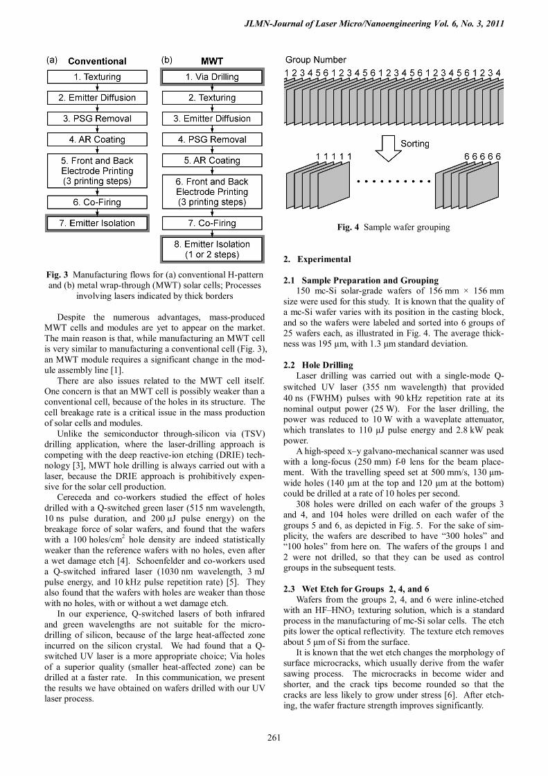
Fig. 3 Manufacturing flows for (a) conventional H-pattern and (b) metal wrap-through (MWT) solar cells; Processes
involving lasers indicated by thick borders Despite the numerous advantages, mass-produced
MWT cells and modules are yet to appear on the market. The main reason is that, while manufacturing an MWT cell is very similar to manufacturing a conventional cell (Fig. 3), an MWT module requires a significant change in the mod-ule assembly line [1].
There are also issues related to the MWT cell itself. One concern is that an MWT cell is possibly weaker than a conventional cell, because of the holes in its structure. The cell breakage rate is a critical issue in the mass production of solar cells and modules.
Unlike the semiconductor through-silicon via (TSV) drilling application, where the laser-drilling approach is competing with the deep reactive-ion etching (DRIE) tech-nology [3], MWT hole drilling is always carried out with a laser, because the DRIE approach is prohibitively expen-sive for the solar cell production.
Cereceda and co-workers studied the effect of holes drilled with a Q-switched green laser (515 nm wavelength, 10 ns pulse duration, and 200 μJ pulse energy) on the breakage force of solar wafers, and found that the wafers with a 100 holes/cm2 hole density are indeed statistically weaker than the reference wafers with no holes, even after a wet damage etch [4]. Schoenfelder and co-workers used a Q-switched infrared laser (1030 nm wavelength, 3 mJ pulse energy, and 10 kHz pulse repetition rate) [5]. They also found that the wafers with holes are weaker than those with no holes, with or without a wet damage etch.
In our experience, Q-switched lasers of both infrared and green wavelengths are not suitable for the micro-drilling of silicon, because of the large heat-affected zone incurred on the silicon crystal. We had found that a Q-switched UV laser is a more appropriate choice; Via holes of a superior quality (smaller heat-affected zone) can be drilled at a faster rate. In this communication, we present the results we have obtained on wafers drilled with our UV laser process.
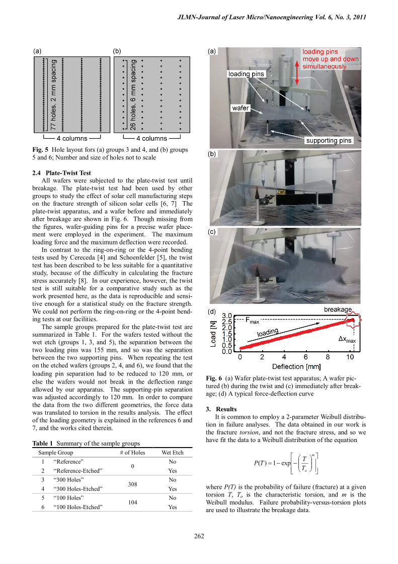
Fig. 4 Sample wafer grouping
2. Experimental
2.1 Sample Preparation and Grouping 150 mc-Si solar-grade wafers of 156 mm × 156 mm
size were used for this study. It is known that the quality of a mc-Si wafer varies with its position in the casting block, and so the wafers were labeled and sorted into 6 groups of 25 wafers each, as illustrated in Fig. 4. The average thick-ness was 195 μm, with 1.3 μm standard deviation.
2.2 Hole Drilling
Laser drilling was carried out with a single-mode Q-switched UV laser (355 nm wavelength) that provided 40 ns (FWHM) pulses with 90 kHz repetition rate at its nominal output power (25 W). For the laser drilling, the power was reduced to 10 W with a waveplate attenuator, which translates to 110 μJ pulse energy and 2.8 kW peak power.
A high-speed x–y galvano-mechanical scanner was used with a long-focus (250 mm) f-θ lens for the beam place-ment. With the travelling speed set at 500 mm/s, 130 μm-wide holes (140 μm at the top and 120 μm at the bottom) could be drilled at a rate of 10 holes per second.
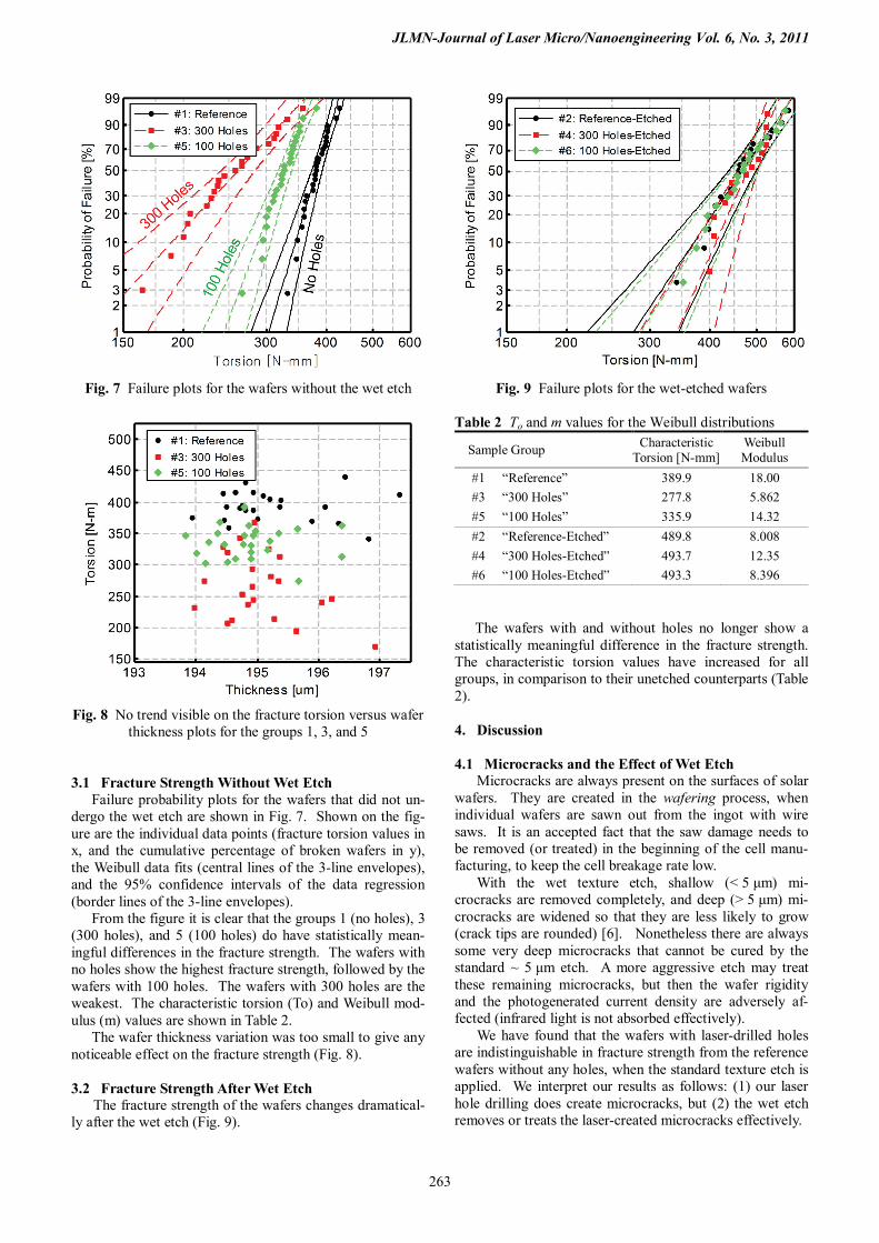
308 holes were drilled on each wafer of the groups 3 and 4, and 104 holes were drilled on each wafer of the groups 5 and 6, as depicted in Fig. 5. For the sake of sim-plicity, the wafers are described to have “300 holes” and “100 holes” from here on. The wafers of the groups 1 and 2 were not drilled, so that they can be used as control groups in the subsequent tests.
2.3 Wet Etch for Groups 2, 4, and 6
Wafers from the groups 2, 4, and 6 were inline-etched with an HF–HNO3 texturing solution, which is a standard process in the manufacturing of mc-Si solar cells. The etch pits lower the optical reflectivity. The texture etch removes about 5 μm of Si from the surface.
It is known that the wet etch changes the morphology of surface microcracks, which usually derive from the wafer sawing process. The microcracks in become wider and shorter, and the crack tips become rounded so that the cracks are less likely to grow under stress [6]. After etch-ing, the wafer fracture strength improves significantly.
JLMN-Journal of Laser Micro/Nanoengineering Vol. 6, No. 3, 2011
262
Fig. 5 Hole layout fors (a) groups 3 and 4, and (b) groups 5 and 6; Number and size of holes not to scale 2.4 Plate-Twist Test
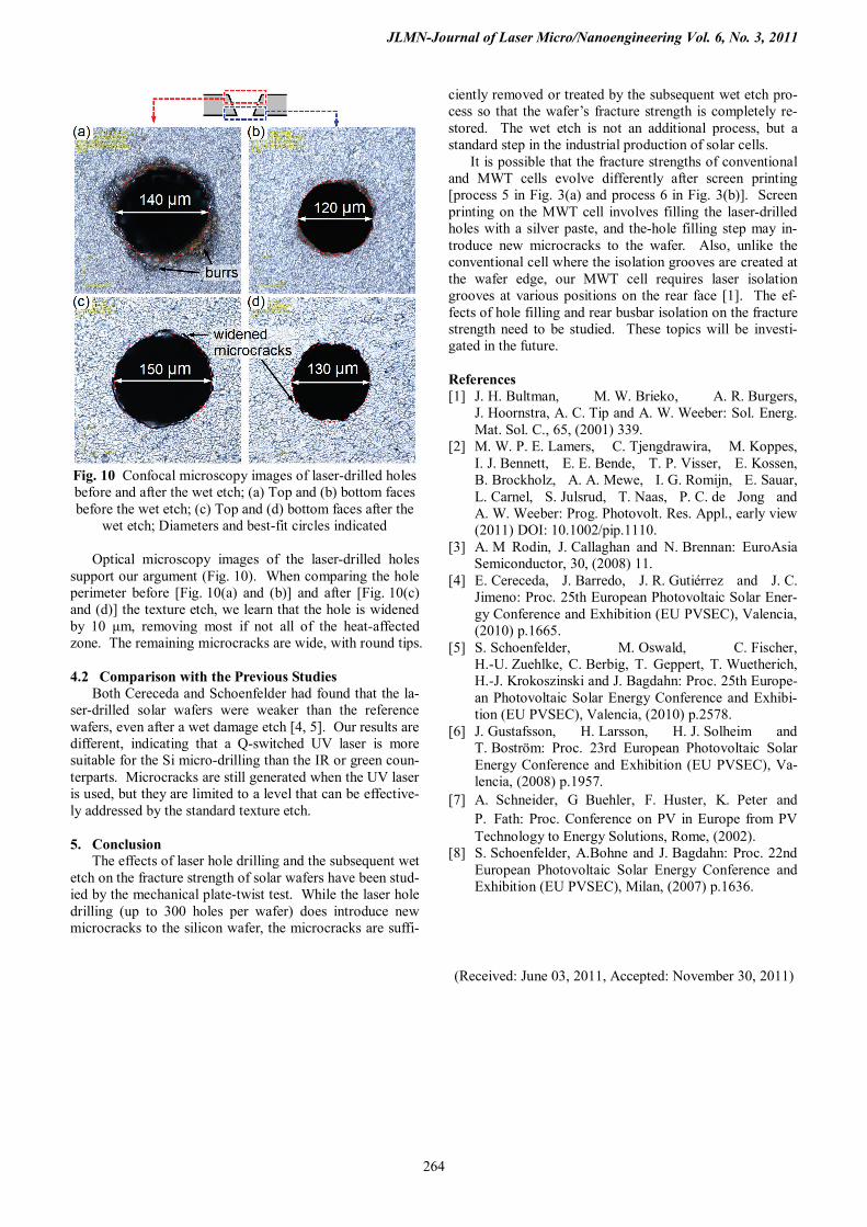
All wafers were subjected to the plate-twist test until breakage. The plate-twist test had been used by other groups to study the effect of solar cell manufacturing steps on the fracture strength of silicon solar cells [6, 7] The plate-twist apparatus, and a wafer before and immediately after breakage are shown in Fig. 6. Though missing from the figures, wafer-guiding pins for a precise wafer place-ment were employed in the experiment. The maximum loading force and the maximum deflection were recorded.
In contrast to the ring-on-ring or the 4-point bending tests used by Cereceda [4] and Schoenfelder [5], the twist test has been described to be less suitable for a quantitative study, because of the difficulty in calculating the fracture stress accurately [8]. In our experience, however, the twist test is still suitable for a comparative study such as the work presented here, as the data is reproducible and sensi-tive enough for a statistical study on the fracture strength. We could not perform the ring-on-ring or the 4-point bend-ing tests at our facilities.
The sample groups prepared for the plate-twist test are summarized in Table 1. For the wafers tested without the wet etch (groups 1, 3, and 5), the separation between the two loading pins was 155 mm, and so was the separation between the two supporting pins. When repeating the test on the etched wafers (groups 2, 4, and 6), we found that the loading pin separation had to be reduced to 120 mm, or else the wafers would not break in the deflection range allowed by our apparatus. The supporting-pin separation was adjusted accordingly to 120 mm. In order to compare the data from the two different geometries, the force data was translated to torsion in the results analysis. The effect of the loading geometry is explained in the references 6 and 7, and the works cited therein.
Table 1 Summary of the sample groups
Sample Group # of Holes Wet Etch 1 “Reference”
0 No
2 “Reference-Etched” Yes 3 “300 Holes”
308 No
4 “300 Holes-Etched” Yes 5 “100 Holes”
104 No
6 “100 Holes-Etched” Yes
Fig. 6 (a) Wafer plate-twist test apparatus; A wafer pic-tured (b) during the twist and (c) immediately after break-age; (d) A typical force-deflection curve
3. Results
It is common to employ a 2-parameter Weibull distribu-tion in failure analyses. The data obtained in our work is the fracture torsion, and not the fracture stress, and so we have fit the data to a Weibull distribution of the equation
−−=
m
oTTTP exp1)(
where P(T) is the probability of failure (fracture) at a given torsion T, To is the characteristic torsion, and m is the Weibull modulus. Failure probability-versus-torsion plots are used to illustrate the breakage data.
JLMN-Journal of Laser Micro/Nanoengineering Vol. 6, No. 3, 2011
263
Fig. 7 Failure plots for the wafers without the wet etch
Fig. 8 No trend visible on the fracture torsion versus wafer
thickness plots for the groups 1, 3, and 5 3.1 Fracture Strength Without Wet Etch
Failure probability plots for the wafers that did not un-dergo the wet etch are shown in Fig. 7. Shown on the fig-ure are the individual data points (fracture torsion values in x, and the cumulative percentage of broken wafers in y), the Weibull data fits (central lines of the 3-line envelopes), and the 95% confidence intervals of the data regression (border lines of the 3-line envelopes).
From the figure it is clear that the groups 1 (no holes), 3 (300 holes), and 5 (100 holes) do have statistically mean-ingful differences in the fracture strength. The wafers with no holes show the highest fracture strength, followed by the wafers with 100 holes. The wafers with 300 holes are the weakest. The characteristic torsion (To) and Weibull mod-ulus (m) values are shown in Table 2.
The wafer thickness variation was too small to give any noticeable effect on the fracture strength (Fig. 8).
3.2 Fracture Strength After Wet Etch
The fracture strength of the wafers changes dramatical-ly after the wet etch (Fig. 9).
Fig. 9 Failure plots for the wet-etched wafers
Table 2 To and m values for the Weibull distributions
Sample Group Characteristic Torsion [N-mm]
Weibull Modulus
#1 “Reference” 389.9 18.00 #3 “300 Holes” 277.8 5.862 #5 “100 Holes” 335.9 14.32 #2 “Reference-Etched” 489.8 8.008 #4 “300 Holes-Etched” 493.7 12.35 #6 “100 Holes-Etched” 493.3 8.396 The wafers with and without holes no longer show a
statistically meaningful difference in the fracture strength. The characteristic torsion values have increased for all groups, in comparison to their unetched counterparts (Table 2).
4. Discussion
4.1 Microcracks and the Effect of Wet Etch
Microcracks are always present on the surfaces of solar wafers. They are created in the wafering process, when individual wafers are sawn out from the ingot with wire saws. It is an accepted fact that the saw damage needs to be removed (or treated) in the beginning of the cell manu-facturing, to keep the cell breakage rate low.
With the wet texture etch, shallow (< 5 μm) mi-crocracks are removed completely, and deep (> 5 μm) mi-crocracks are widened so that they are less likely to grow (crack tips are rounded) [6]. Nonetheless there are always some very deep microcracks that cannot be cured by the standard ~ 5 μm etch. A more aggressive etch may treat these remaining microcracks, but then the wafer rigidity and the photogenerated current density are adversely af-fected (infrared light is not absorbed effectively).
We have found that the wafers with laser-drilled holes are indistinguishable in fracture strength from the reference wafers without any holes, when the standard texture etch is applied. We interpret our results as follows: (1) our laser hole drilling does create microcracks, but (2) the wet etch removes or treats the laser-created microcracks effectively.
JLMN-Journal of Laser Micro/Nanoengineering Vol. 6, No. 3, 2011
264
Fig. 10 Confocal microscopy images of laser-drilled holes before and after the wet etch; (a) Top and (b) bottom faces before the wet etch; (c) Top and (d) bottom faces after the
wet etch; Diameters and best-fit circles indicated Optical microscopy images of the laser-drilled holes
support our argument (Fig. 10). When comparing the hole perimeter before [Fig. 10(a) and (b)] and after [Fig. 10(c) and (d)] the texture etch, we learn that the hole is widened by 10 μm, removing most if not all of the heat-affected zone. The remaining microcracks are wide, with round tips. 4.2 Comparison with the Previous Studies
Both Cereceda and Schoenfelder had found that the la-ser-drilled solar wafers were weaker than the reference wafers, even after a wet damage etch [4, 5]. Our results are different, indicating that a Q-switched UV laser is more suitable for the Si micro-drilling than the IR or green coun-terparts. Microcracks are still generated when the UV laser is used, but they are limited to a level that can be effective-ly addressed by the standard texture etch.
5. Conclusion
The effects of laser hole drilling and the subsequent wet etch on the fracture strength of solar wafers have been stud-ied by the mechanical plate-twist test. While the laser hole drilling (up to 300 holes per wafer) does introduce new microcracks to the silicon wafer, the microcracks are suffi-
ciently removed or treated by the subsequent wet etch pro-cess so that the wafer’s fracture strength is completely re-stored. The wet etch is not an additional process, but a standard step in the industrial production of solar cells.
It is possible that the fracture strengths of conventional and MWT cells evolve differently after screen printing [process 5 in Fig. 3(a) and process 6 in Fig. 3(b)]. Screen printing on the MWT cell involves filling the laser-drilled holes with a silver paste, and the-hole filling step may in-troduce new microcracks to the wafer. Also, unlike the conventional cell where the isolation grooves are created at the wafer edge, our MWT cell requires laser isolation grooves at various positions on the rear face [1]. The ef-fects of hole filling and rear busbar isolation on the fracture strength need to be studied. These topics will be investi-gated in the future.
References [1] J. H. Bultman, M. W. Brieko, A. R. Burgers,
J. Hoornstra, A. C. Tip and A. W. Weeber: Sol. Energ. Mat. Sol. C., 65, (2001) 339.
[2] M. W. P. E. Lamers, C. Tjengdrawira, M. Koppes, I. J. Bennett, E. E. Bende, T. P. Visser, E. Kossen, B. Brockholz, A. A. Mewe, I. G. Romijn, E. Sauar, L. Carnel, S. Julsrud, T. Naas, P. C. de Jong and A. W. Weeber: Prog. Photovolt. Res. Appl., early view (2011) DOI: 10.1002/pip.1110.
[3] A. M Rodin, J. Callaghan and N. Brennan: EuroAsia Semiconductor, 30, (2008) 11.
[4] E. Cereceda, J. Barredo, J. R. Gutiérrez and J. C. Jimeno: Proc. 25th European Photovoltaic Solar Ener-gy Conference and Exhibition (EU PVSEC), Valencia, (2010) p.1665.
[5] S. Schoenfelder, M. Oswald, C. Fischer, H.-U. Zuehlke, C. Berbig, T. Geppert, T. Wuetherich, H.-J. Krokoszinski and J. Bagdahn: Proc. 25th Europe-an Photovoltaic Solar Energy Conference and Exhibi-tion (EU PVSEC), Valencia, (2010) p.2578.
[6] J. Gustafsson, H. Larsson, H. J. Solheim and T. Boström: Proc. 23rd European Photovoltaic Solar Energy Conference and Exhibition (EU PVSEC), Va-lencia, (2008) p.1957.
[7] A. Schneider, G Buehler, F. Huster, K. Peter and P. Fath: Proc. Conference on PV in Europe from PV Technology to Energy Solutions, Rome, (2002).
[8] S. Schoenfelder, A.Bohne and J. Bagdahn: Proc. 22nd European Photovoltaic Solar Energy Conference and Exhibition (EU PVSEC), Milan, (2007) p.1636.
(Received: June 03, 2011, Accepted: November 30, 2011)