Embed Size (px)
Citation preview

University of California
Los Angeles
High-Speed, Low-Power Analog-to-Digital
Converters
A dissertation submitted in partial satisfaction
of the requirements for the degree
Doctor of Philosophy in Electrical Engineering
by
Shiuh-hua Chiang
2013

c© Copyright by
Shiuh-hua Chiang
2013
Abstract of the Dissertation
High-Speed, Low-Power Analog-to-Digital
Converters
by
Shiuh-hua Chiang
Doctor of Philosophy in Electrical Engineering
University of California, Los Angeles, 2013
Professor Behzad Razavi, Chair
Analog-to-digital converters (ADCs) are widely used in communication sys-
tems to interface analog and digital circuits. While the speed, power, and area
of digital circuits directly benefit from the decreasing channel length of CMOS
devices, analog circuits suffer from reduced headroom, lower intrinsic gain, and
higher device mismatch. Consequently, it has been increasingly difficult to design
high-speed and low-power pipelined ADCs using conventional op amps.
This work presents a pipelined ADC that employs novel charge-steering op
amps to relax the trade-offs among speed, noise, and power consumption. Such
op amps afford a fourfold increase in speed and a twofold reduction in noise for a
given power consumption and voltage gain. Using a new clock gating technique,
the ADC digitally calibrates the nonlinearity and gain error at full speed. A
prototype realized in 65-nm CMOS technology achieves a resolution of 10 bits
with a sampling rate of 800 MHz, a power consumption of 19 mW, an SNDR of
52.2 dB at Nyquist, and an FoM of 53 fJ/conversion-step. A new background
calibration technique is also proposed to accommodate temperature and supply
variations.
ii

The dissertation of Shiuh-hua Chiang is approved.
Milos Ercegovac
William Kaiser
Frank Chang
Behzad Razavi, Committee Chair
University of California, Los Angeles
2013
iii

To my lovely wife
Camilla
and our darlings
iv

Table of Contents
1 Introduction . . . . . . . . . . . . . . . . . . . . . . . . . . . . . . . . 1
2 ADC Architectures . . . . . . . . . . . . . . . . . . . . . . . . . . . 3
2.1 Overview . . . . . . . . . . . . . . . . . . . . . . . . . . . . . . . . 3
2.2 Flash ADC . . . . . . . . . . . . . . . . . . . . . . . . . . . . . . 3
2.3 SAR ADC . . . . . . . . . . . . . . . . . . . . . . . . . . . . . . . 4
2.4 Sigma-Delta ADC . . . . . . . . . . . . . . . . . . . . . . . . . . . 5
2.5 Pipelined ADC . . . . . . . . . . . . . . . . . . . . . . . . . . . . 5
2.6 Discussion . . . . . . . . . . . . . . . . . . . . . . . . . . . . . . . 6
3 Pipelined ADC . . . . . . . . . . . . . . . . . . . . . . . . . . . . . . 7
3.1 Overview . . . . . . . . . . . . . . . . . . . . . . . . . . . . . . . . 7
3.2 Stage Non-Idealities . . . . . . . . . . . . . . . . . . . . . . . . . . 10
3.2.1 Comparator Offset . . . . . . . . . . . . . . . . . . . . . . 11
3.2.2 DAC Offset . . . . . . . . . . . . . . . . . . . . . . . . . . 12
3.2.3 DAC Gain Error . . . . . . . . . . . . . . . . . . . . . . . 13
3.2.4 DAC Nonlinearity . . . . . . . . . . . . . . . . . . . . . . . 16
3.2.5 Op Amp Offset . . . . . . . . . . . . . . . . . . . . . . . . 16
3.2.6 Op Amp Gain Error . . . . . . . . . . . . . . . . . . . . . 17
3.2.7 Op Amp Nonlinearity . . . . . . . . . . . . . . . . . . . . . 18
3.3 Discussion . . . . . . . . . . . . . . . . . . . . . . . . . . . . . . . 21
4 Charge-Steering Op Amp . . . . . . . . . . . . . . . . . . . . . . . 23
4.1 Overview . . . . . . . . . . . . . . . . . . . . . . . . . . . . . . . . 23
v

4.2 Charge-Steering Op Amp Operation . . . . . . . . . . . . . . . . . 24
4.3 Charge-Steering Op Amp Gain Analysis . . . . . . . . . . . . . . 27
4.4 Charge-Steering Op Amp Noise Analysis . . . . . . . . . . . . . . 29
4.4.1 Mathematical Background . . . . . . . . . . . . . . . . . . 29
4.4.2 Noise in the Reset Phase . . . . . . . . . . . . . . . . . . . 34
4.4.3 Noise in the Amplification Phase . . . . . . . . . . . . . . 35
4.4.4 Noise in the Hold Phase . . . . . . . . . . . . . . . . . . . 37
4.4.5 Input-Referred Noise Voltage Variance . . . . . . . . . . . 38
4.4.6 Closed-Loop Op Amp Noise . . . . . . . . . . . . . . . . . 39
4.5 Closed-Loop Charge-Steering Op Amp . . . . . . . . . . . . . . . 40
4.5.1 Overview . . . . . . . . . . . . . . . . . . . . . . . . . . . 40
4.5.2 Closed-Loop Model . . . . . . . . . . . . . . . . . . . . . . 40
4.6 Op Amp Comparison . . . . . . . . . . . . . . . . . . . . . . . . . 41
5 Prototype ADC Design . . . . . . . . . . . . . . . . . . . . . . . . . 44
5.1 ADC Architecture . . . . . . . . . . . . . . . . . . . . . . . . . . . 44
5.2 Calibration . . . . . . . . . . . . . . . . . . . . . . . . . . . . . . 47
5.2.1 Overview . . . . . . . . . . . . . . . . . . . . . . . . . . . 47
5.2.2 Proposed Foreground Calibration . . . . . . . . . . . . . . 48
5.2.3 Proposed Background Calibration . . . . . . . . . . . . . . 54
5.3 Proposed Common-Mode Feedback . . . . . . . . . . . . . . . . . 58
5.4 Circuit Building Blocks . . . . . . . . . . . . . . . . . . . . . . . . 60
5.4.1 Stage 1 . . . . . . . . . . . . . . . . . . . . . . . . . . . . . 60
5.4.2 Stage 2 . . . . . . . . . . . . . . . . . . . . . . . . . . . . . 61
5.4.3 Stage 3 . . . . . . . . . . . . . . . . . . . . . . . . . . . . . 63
vi

5.4.4 Backend Stages . . . . . . . . . . . . . . . . . . . . . . . . 64
5.4.5 Reference Generation . . . . . . . . . . . . . . . . . . . . . 65
5.4.6 Bootstrapping Circuit . . . . . . . . . . . . . . . . . . . . 66
5.4.7 Comparator . . . . . . . . . . . . . . . . . . . . . . . . . . 68
5.4.8 Calibration DAC . . . . . . . . . . . . . . . . . . . . . . . 68
5.4.9 Clock Generator . . . . . . . . . . . . . . . . . . . . . . . 69
6 Experimental Results . . . . . . . . . . . . . . . . . . . . . . . . . . 72
6.1 Test Setup . . . . . . . . . . . . . . . . . . . . . . . . . . . . . . . 72
6.2 Measurement Results . . . . . . . . . . . . . . . . . . . . . . . . . 74
7 Conclusion and Future Work . . . . . . . . . . . . . . . . . . . . . 79
References . . . . . . . . . . . . . . . . . . . . . . . . . . . . . . . . . . . 81
vii

List of Figures
2.1 Flash ADC. . . . . . . . . . . . . . . . . . . . . . . . . . . . . . . 3
2.2 SAR ADC. . . . . . . . . . . . . . . . . . . . . . . . . . . . . . . 4
2.3 Sigma-delta ADC. . . . . . . . . . . . . . . . . . . . . . . . . . . . 5
2.4 Pipelined ADC. . . . . . . . . . . . . . . . . . . . . . . . . . . . . 6
3.1 Input processing in a pipelined ADC. . . . . . . . . . . . . . . . . 7
3.2 Circuit implementation of a pipelined stage. . . . . . . . . . . . . 8
3.3 Input-output transfer characteristic of a 1-bit stage. . . . . . . . . 9
3.4 Input-output transfer characteristic of a differential 1-bit Stage. . 10
3.5 Input-output transfer characteristic of a 1.5-bit stage. . . . . . . . 10
3.6 Effect of comparator offsets on stage transfer characteristic. . . . . 11
3.7 Effect of comparator offsets on ADC transfer characteristic. . . . . 12
3.8 Effect of DAC offset on stage transfer characteristic. . . . . . . . . 13
3.9 Effect of DAC offset on ADC transfer characteristic. . . . . . . . . 13
3.10 Effect of DAC gain error on stage transfer characteristic, gain >
ideal gain. . . . . . . . . . . . . . . . . . . . . . . . . . . . . . . . 14
3.11 Effect of DAC gain error on ADC transfer characteristic, gain >
ideal gain. . . . . . . . . . . . . . . . . . . . . . . . . . . . . . . . 14
3.12 Effect of DAC gain error on stage transfer characteristic, gain <
ideal gain. . . . . . . . . . . . . . . . . . . . . . . . . . . . . . . . 15
3.13 Effect of DAC gain error on ADC transfer characteristic, gain <
ideal gain. . . . . . . . . . . . . . . . . . . . . . . . . . . . . . . . 15
3.14 Effect of DAC non-linearity on stage transfer characteristic. . . . . 16
3.15 Effect of DAC non-linearity on ADC transfer characteristic. . . . 17
viii

3.16 Effect of op amp offset on stage transfer characteristic. . . . . . . 17
3.17 Effect of op amp offset on ADC transfer characteristic. . . . . . . 18
3.18 Effect of op amp gain error on stage transfer characteristic, gain >
ideal gain. . . . . . . . . . . . . . . . . . . . . . . . . . . . . . . . 19
3.19 Effect of op amp gain error on ADC transfer characteristic, gain >
ideal gain. . . . . . . . . . . . . . . . . . . . . . . . . . . . . . . . 19
3.20 Effect of op amp gain error on stage transfer characteristic, gain <
ideal gain. . . . . . . . . . . . . . . . . . . . . . . . . . . . . . . . 20
3.21 Effect of op amp gain error on ADC transfer characteristic, gain <
ideal gain. . . . . . . . . . . . . . . . . . . . . . . . . . . . . . . . 20
3.22 Effect of op amp nonlinearity on stage transfer characteristic. . . . 21
3.23 Effect of op amp nonlinearity on ADC transfer characteristic. . . . 21
4.1 Transformation from current-steering to charge-steering. . . . . . 23
4.2 One-stage CS op amp during the (a) reset and (b) amplification
phases. . . . . . . . . . . . . . . . . . . . . . . . . . . . . . . . . . 24
4.3 One-stage CS op amp output vs time in (a) single-ended and (b)
differential views. . . . . . . . . . . . . . . . . . . . . . . . . . . . 25
4.4 Two-stage CS op amp during the (a) reset and (b) amplification
phases. . . . . . . . . . . . . . . . . . . . . . . . . . . . . . . . . . 25
4.5 Two-stage CS op amp output vs time in (a) single-ended and (b)
differential views. . . . . . . . . . . . . . . . . . . . . . . . . . . . 26
4.6 Two-stage CS op amp during the hold phase. . . . . . . . . . . . 27
4.7 Charge-steering op amp. . . . . . . . . . . . . . . . . . . . . . . . 27
4.8 Equivalent half-circuit of the op amp in the amplification phase. . 27
4.9 Op amp transconductance versus time. . . . . . . . . . . . . . . . 28
ix

4.10 Noise in an RC circuit . . . . . . . . . . . . . . . . . . . . . . . . 29
4.11 Equivalent half-circuit of the op amp in the reset phase. . . . . . . 34
4.12 Equivalent half-circuit of the op amp in the amplification phase. . 35
4.13 Equivalent half-circuit of the op amp in the hold phase. . . . . . . 37
4.14 Op amp noise in closed-loop. . . . . . . . . . . . . . . . . . . . . . 39
4.15 Closed-loop op amp. . . . . . . . . . . . . . . . . . . . . . . . . . 40
4.16 (a) Model of the closed-loop CS op amp and (b) its step response. 41
4.17 Conventional one-stage op amp. . . . . . . . . . . . . . . . . . . . 42
4.18 Conventional two-stage op amp. . . . . . . . . . . . . . . . . . . . 42
4.19 Closed-loop setup for op amp comparison. . . . . . . . . . . . . . 42
4.20 Op amp step response comparison. . . . . . . . . . . . . . . . . . 43
5.1 Input-output characteristic of (a) 1.5-bit and (b) 2.5-bit topologies. 45
5.2 Stage 1 input-output transfer characteristic. . . . . . . . . . . . . 46
5.3 Proposed ADC architecture. . . . . . . . . . . . . . . . . . . . . . 46
5.4 ADC calibration using (a) analog only, (b) digital only, and (c)
mixed-signal techniques. . . . . . . . . . . . . . . . . . . . . . . . 47
5.5 Digital calibration of ADC. . . . . . . . . . . . . . . . . . . . . . 48
5.6 Stages 5-13 calibration. . . . . . . . . . . . . . . . . . . . . . . . . 49
5.7 Stage 4 calibration. . . . . . . . . . . . . . . . . . . . . . . . . . . 49
5.8 Stage 2 calibration. . . . . . . . . . . . . . . . . . . . . . . . . . . 50
5.9 Stage 1 calibration. . . . . . . . . . . . . . . . . . . . . . . . . . . 50
5.10 Calibration of Stages 1, 2 as one block. . . . . . . . . . . . . . . . 51
5.11 Calibration voltage path. . . . . . . . . . . . . . . . . . . . . . . . 51
5.12 Full-speed calibration by gated clock. . . . . . . . . . . . . . . . . 52
x

5.13 Simulated settling of calibration voltage. . . . . . . . . . . . . . . 53
5.14 Charge injection of the sampling switch. . . . . . . . . . . . . . . 53
5.15 Stage 1 input-output characteristics at 27 and 60 C. . . . . . . . 54
5.16 Change in Stage 1’s input-output characteristic from 27 to 60 C. 55
5.17 ADC output histogram at 60C. . . . . . . . . . . . . . . . . . . . 56
5.18 Background calibration procedure. . . . . . . . . . . . . . . . . . 56
5.19 DNL and INL before and after background calibration for temper-
ature compensation. . . . . . . . . . . . . . . . . . . . . . . . . . 57
5.20 Change in Stage 1’s input-output characteristic from VDD = 1.00
V to 1.01 V. . . . . . . . . . . . . . . . . . . . . . . . . . . . . . . 58
5.21 DNL and INL before and after background calibration for supply
compensation. . . . . . . . . . . . . . . . . . . . . . . . . . . . . . 59
5.22 Conventional common-mode control. . . . . . . . . . . . . . . . . 59
5.23 Proposed common-mode control. . . . . . . . . . . . . . . . . . . 60
5.24 Stage 1 design. . . . . . . . . . . . . . . . . . . . . . . . . . . . . 62
5.25 Stage 2 design. . . . . . . . . . . . . . . . . . . . . . . . . . . . . 63
5.26 Stage 3 design. . . . . . . . . . . . . . . . . . . . . . . . . . . . . 65
5.27 Stage 1 MDAC reference generation. . . . . . . . . . . . . . . . . 66
5.28 Bootstrapping circuit . . . . . . . . . . . . . . . . . . . . . . . . . 67
5.29 Comparator . . . . . . . . . . . . . . . . . . . . . . . . . . . . . . 68
5.30 Calibration DAC layout. . . . . . . . . . . . . . . . . . . . . . . . 69
5.31 Conventional clock generator. . . . . . . . . . . . . . . . . . . . . 69
5.32 Conventional non-overlap generator. . . . . . . . . . . . . . . . . . 70
5.33 Proposed clock generator. . . . . . . . . . . . . . . . . . . . . . . 70
5.34 Proposed non-overlap generator. . . . . . . . . . . . . . . . . . . . 71
xi

6.1 Chip photograph. . . . . . . . . . . . . . . . . . . . . . . . . . . . 72
6.2 PCB layout. . . . . . . . . . . . . . . . . . . . . . . . . . . . . . . 73
6.3 ADC test setup. . . . . . . . . . . . . . . . . . . . . . . . . . . . . 74
6.4 DNL before and after calibration. . . . . . . . . . . . . . . . . . . 75
6.5 INL before and after calibration. . . . . . . . . . . . . . . . . . . . 75
6.6 Output spectrum with fin = 9.8 MHz. . . . . . . . . . . . . . . . 76
6.7 Output spectrum with fin = 399.2 MHz. . . . . . . . . . . . . . . 76
6.8 SNDR vs fin. . . . . . . . . . . . . . . . . . . . . . . . . . . . . . 77
6.9 FoM comparison. . . . . . . . . . . . . . . . . . . . . . . . . . . . 78
xii

List of Tables
4.1 Op amp performance comparison. . . . . . . . . . . . . . . . . . . 43
5.1 Stage topology parameters and comparison. . . . . . . . . . . . . 45
6.1 Performance summary and comparison. . . . . . . . . . . . . . . . 77
xiii

Acknowledgments
I would like to express my gratitude to my advisor Prof. Behzad Razavi for his
guidance and support throughout my studies at UCLA. His experience, insight,
patience, and perseverance have taught me lessons that I will closely and dearly
keep for a lifetime.
I would like to express my gratitude to my committee members Prof. Frank
Chang, Prof. William Kaiser, and Prof. Milos Ercegovac for their valuable input
and time.
I would like to express my gratitude to Dr. Yaozhong Liu and Dr. Yichi Shih
from Honeywell. They have invested much time and energy to ensure the success
of this work.
I would like to express my gratitude to my colleagues: Ali Homayoun, Ashutosh
Verma, Bibhu Sahoo, Brian Lee, Chris Liu, Hegong Wei, Jithin Janardhan, Joseph
Matthew, Joung Won Park, Jun Won Jung, Marco Zanuso, Sedigheh Hashemi,
Steven Hwu, and Tim Sun. Special thanks to Tim Sun for the layout assistance.
I would like to express my gratitude to my past mentors who guided my studies
and inspired me to pursue the Ph.D. degree: Prof. Stuart Kleinfelder (University
of California, Irvine), Prof. John Yeow, Prof. Patricia Nieva, and Prof. Adel
Sedra (all with University of Waterloo, Canada).
I would like to express my gratitude to my parents and parents-in-law for their
kind support. This work would not be possible without them.
I would like to express my gratitude to my kids, who brought heavenly sunshine
and angelic smiles into our home. Their radiant faces and giggles are a panacea
to all my research headaches.
Above all, I would like to express my gratitude to my darling wife, Camilla,
for her encouragement, support, and sacrifice throughout all these years. She
xiv

deserves a name beside mine on the face of this dissertation. She has been, and
always will be, the highlight of my life since the very first day I met her. I look
forward to sharing many more highlights with her in all the years to come.
xv

CHAPTER 1
Introduction
Communication systems such as cellular radios, fiber optic links, and cable modems
employ analog-to-digital converters (ADCs) in their receivers to convert analog
signals to digital signals. Recently there is a growing trend in building all-digital
receivers by moving the ADC, traditionally placed at the end of the receiver chain,
closer to the frontend [1, 2]. By doing so many of the analog circuits, such as mix-
ers and filters, can be implemented digitally to benefit directly from technology
scaling.
Pipelined ADCs are suitable for many receiver applications due to their high
speeds [3, 4, 5, 6]. However, high-performance and low-power op amps in pipelined
ADCs are increasingly harder to build as CMOS process technology scales down.
The reduced supply voltage in a scaled technology limits the maximum swing
that an op amp can achieve, therefore degrading the op amp’s signal-to-noise
ratio. Also, the lowered headroom makes it difficult to use stacked topologies,
such as cascodes, to boost an op amp’s gain. Furthermore, the intrinsic gain
gmro of a transistor continues to decrease with each new generation of process
technology. At the 65-nm node, gmro is less than 10. Therefore, pipelined ADCs
that use conventional op amps face stringent trade-offs among noise, gain, power,
and speed. A typical pipelined ADC consumes more than 70% of its power in the
op amps [7].
This work addresses the challenges faced by today’s pipelined ADCs by using
a new “charge-steering” op amp topology. This new op amp offers a fourfold
1

increase in speed and a twofold reduction in noise for a given power consumption
and voltage gain. This work also proposes a new op amp common-mode feedback
technique that avoids the power and speed penalties of the conventional methods.
A novel clock-gating technique allows foreground calibration of the op amp at
the full ADC clock rate. A 10-bit ADC using these techniques is designed and
fabricated in 65-nm CMOS technology. The ADC achieves an SNDR of 52.2
dB at 800-MHz sampling frequency with a 399.2-MHz input and an FoM of 53
fJ/conversion-step. A new background calibration technique is also proposed to
compensate for temperature and supply variations.
This thesis is organized as follows: Chapter 2 reviews the different ADC ar-
chitectures. Chapter 3 discusses the pipelined ADC design trade-offs and non-
idealities. Chapter 4 presents the design and analysis of the proposed charge-
steering op amp. Chapter 5 describes the proposed ADC architecture, its fore-
ground and background calibration techniques, a new common-mode feedback
technique, and the circuit building blocks. Chapter 6 shows the experimental re-
sults. Chapter 7 summarizes this work’s contributions and proposes future work.
2

CHAPTER 2
ADC Architectures
2.1 Overview
There are several major types of ADC architectures. Each type entails different
trade-offs among speed, accuracy, power, and area. The following sections examine
the different types of ADCs and discuss their trade-offs.
2.2 Flash ADC
A flash ADC uses full parallelism to quantize the input, achieving a high conver-
sion rate at the cost of a high number of comparators. A flash ADC contains an
array of comparators, a resistor ladder that generates the reference voltages, and
a thermometer-to-binary converter (Fig. 2.1).
The
rmom
eter
to B
inar
y
inV
Vr1
V
V
r2
r3
Dout
Figure 2.1: Flash ADC.
3

The comparators compare the input against the references, and produce a
thermometer code which is a quantized version of the input. Because all the com-
parators work in parallel, the conversion is completed in one clock cycle. However
a flash ADC suffers from limited resolution because the number of comparators
and reference levels grow exponentially with the resoltuion. For an N -bit flash
ADC, 2N − 1 comparators and reference levels are required. Furthermore, as
the resolution increases the size of the comparators must be scaled up to meet
the matching requirement. Therefore, the area and power consumption typically
limit a flash ADC’s resolution to 8 bits or less, while its speed can reach several
gigahertz.
2.3 SAR ADC
A successive-approximation register (SAR) ADC recursively uses a single com-
parator to quantize the input, achieving power and area savings at the expense of
speed. The SAR ADC consists of a comparator, a state machine, and a digital-
to-analog convertor (DAC) (Fig. 2.2).
StateMachine
inV
DAC
Dout
Figure 2.2: SAR ADC.
Using a binary search, Dout is adjusted until the DAC output converges to
the analog input. Because the binary search proceeds serially, it takes N clock
cycles to resolve N bits. Therefore, a SAR ADC’s speed is typically limited to
tens of megahertz while the resolution can reach as high as 14 bits. The area is
dominated by the DAC due to matching requirement.
4

2.4 Sigma-Delta ADC
A sigma-delta ADC achieves high resolution by forcing the quantization error to
zero with a negative feedback, but suffers from limited speed due to the need to
oversample. A sigma-delta ADC consists of an integrator, a comparator, a DAC,
and a digital filter (Fig. 2.3).
DAC
outDFilter
DigitalinV
Figure 2.3: Sigma-delta ADC.
The error between the input and the DAC output is integrated, then quantized
to 1 bit by the comparator. The negative feedback loop forces the time-average
of the comparator output to converge to the input. The digital filter decimates
the comparator output and removes the unwanted out-of-band energy. A sigma-
delta ADC can achieve a high resolution in the range of 14 to 20 bits, but its
bandwidth is limited to tens of megahertz due to the required oversampling for
time-averaging.
2.5 Pipelined ADC
A pipelined ADC balances the speed advantage offered by parallelism and area
savings by serialism. A pipelined ADC consists of a cascade of pipelined stages,
each containing a sub-ADC, a DAC, a subtractor, and an op amp. (Fig. 2.4).
A stage processes its input in the following manner. First, the k-bit sub-ADC
quantizes the input Vi. Then the DAC converts the sub-ADC’s digital output to
the analog domain. The subtractor subtracts the output of the DAC from the
5

SubADC
2 k
k
DAC
V V
S 1 S S2
Vin
M
k
D1
V1 V2 VM−1
k
D
k
D2 M
i i+1
D Stage Viewi
Figure 2.4: Pipelined ADC.
input. Lastly, the op amp amplifies the subtractor’s output, which becomes the
input Vi+1 of the next stage. The combined digital outputs of all the sub-ADCs
form the final ADC output. For an N -bit ADC, the required number of stages is
N/k where k is the resolution of the sub-ADC in each stage. Because all pipelined
stages work concurrently, the conversion speed of a pipelined ADC is high. At
the same time, the number of circuit elements scales linearity with the resolution.
The disadvantage of pipelined ADCs is the stringent op amp requirements, which
translate to high power consumption. A pipelined ADC can reach 12-bit resolution
and several hundred-megahertz speed.
2.6 Discussion
The above overview shows that the pipelined architecture is a suitable candidate
for high-speed and medium-resolution specifications . However, the stringent re-
quirements placed on the op amps leads to severe trade-offs among speed, gain,
noise, and power. The next section discusses the op amp design issues and non-
idealities in a pipelined ADC.
6

CHAPTER 3
Pipelined ADC
3.1 Overview
The pipelined ADC uses a cascade of stages to resolve the input. Fig. 3.1 shows
how the input is processed in an example 4-stage, 1-bit-per-stage pipelined ADC.
VREF
V
2REF
0
1 S S S2 3 4S
"1" "0" "1" "1"
Figure 3.1: Input processing in a pipelined ADC.
Stage 1 (S1) compares the input (black dot) to the reference level VREF/2.
Since the input is larger than the reference level, S1 outputs a digital “1” and
subtracts VREF/2 from the input. S1 then amplifies the difference (residue) by a
factor of two (grey arrows) and applies the result to the next stage. S2 repeats
the same steps: S2 compares its input to VREF/2. Because S2’s input is smaller
than VREF/2, S2 outputs a digital “0” and subtracts nothing from S2’s input.
S2 amplifies its residue and applies the result to S3. S3 and S4 follow the same
steps, with their digital outputs being “1” and “1”. Note that each stage provides
increasingly finer resolution of the input as it travels further down the pipelined
7
chain. The resulting string of digital values, “1011” (the most significant bit being
from S1), is the digital representation of the analog input. In general, each stage
can resolve k bits using 2k − 1 comparison levels, 2k subtraction levels, and a
2k amplification factor. The overall resolution of the ADC is the summation of
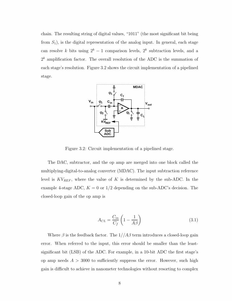
each stage’s resolution. Figure 3.2 shows the circuit implementation of a pipelined
stage.
C f
C in1φ
2φ
VoutVin
REFKV
φ1
SubADC
A
MDAC
LCφ1
Figure 3.2: Circuit implementation of a pipelined stage.
The DAC, subtractor, and the op amp are merged into one block called the
multiplying-digital-to-analog converter (MDAC). The input subtraction reference
level is KVREF , where the value of K is determined by the sub-ADC. In the
example 4-stage ADC, K = 0 or 1/2 depending on the sub-ADC’s decision. The
closed-loop gain of the op amp is
ACL =CinCf
(
1 − 1
Aβ
)
(3.1)
Where β is the feedback factor. The 1//Aβ term introduces a closed-loop gain
error. When referred to the input, this error should be smaller than the least-
significant bit (LSB) of the ADC. For example, in a 10-bit ADC the first stage’s
op amp needs A > 3000 to sufficiently suppress the error. However, such high
gain is difficult to achieve in nanometer technologies without resorting to complex
8

op amp topologies such as cascoding, cascading, and gain boosting, all of which
lead to large noise and high power consumption. Besides gain, the speed of the
op amp is also of concern. The settling time τ of the closed-loop op amp is
τ =CeqGmβ
(3.2)
Where Ceq is the equivalent capacitance see by the output node, and Gm is
the transconductance of the amplifier. For a 10-bit ADC, the required time for
the first stage’s op amp to settle is > 8τ . In order to increase speed, τ must be
reduced. Since the minimum Ceq is typically limited by thermal noise, Gm must be
increased, resulting in higher power consumption. The next chapter will present
a new op amp topology that alleviates the gain, speed, and power trade-offs.
VREF
VR
EF
Vin
Vout
0
RE
F/
V2
Figure 3.3: Input-output transfer characteristic of a 1-bit stage.
9

VREF
VREF
VR
EF
VR
EF
Vin
Vout
0
0
Figure 3.4: Input-output transfer characteristic of a differential 1-bit Stage.
VREF
VREF
VR
EF
VR
EF
Vin
Vout
REF /V 2
REF /V 2
RE
F/
V4
RE
F/
V4 0
0
Figure 3.5: Input-output transfer characteristic of a 1.5-bit stage.
3.2 Stage Non-Idealities
The input-output transfer characteristic of a 1-bit stage is shown in Fig. 3.3,
and the differential version is shown in Fig. 3.4. To add redundancy, Lewis et
10

al. proposed adding one more comparator to the sub-ADC in a 1-bit stage. The
redundancy provides large tolerances to comparator offsets [8]. The input-output
transfer characteristic of this new stage topology, called the 1.5-bit stage, is shown
in Fig. 3.5. This section examines the effects of stage errors on the ADC’s input-
output transfer characteristics.
3.2.1 Comparator Offset
Comparator offsets come from device threshold mismatch, device noise, capacitor
mismatch, reference error, MDAC and sub-ADC path mismatch, and sampling
clock jitter. Comparator offsets shift the locations of the vertical lines in a stage’s
input-output transfer characteristic, as shown in Fig. 3.6 (grey lines indicate the
transfer characteristic after the offset).
VREF
VREF
VR
EF
VR
EF
Vin
Vout
REF /V 2
REF /V 2
RE
F/
V4
RE
F/
V4 0
0
Figure 3.6: Effect of comparator offsets on stage transfer characteristic.
With the redundant stage architecture, the effect of comparator offset is benign
so long as the offset does not exceed the offset correction range, which is the
maximum offset that a stage can tolerate before the output exceeds ±VREF . In the
11
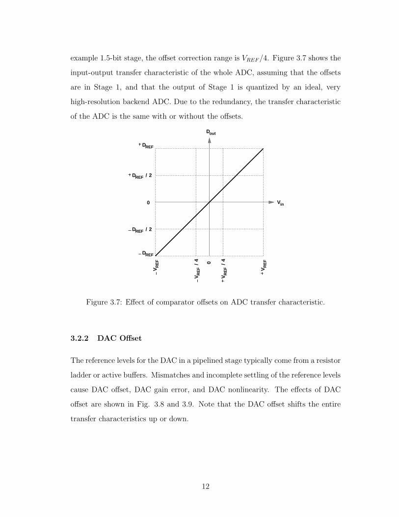
example 1.5-bit stage, the offset correction range is VREF/4. Figure 3.7 shows the
input-output transfer characteristic of the whole ADC, assuming that the offsets
are in Stage 1, and that the output of Stage 1 is quantized by an ideal, very
high-resolution backend ADC. Due to the redundancy, the transfer characteristic
of the ADC is the same with or without the offsets.
REF
REF
VR
EF
VR
EF
Vin
out
REF / 2
REF / 2
RE
F/
V4
RE
F/
V4 0
0
D
D
D
D
D
Figure 3.7: Effect of comparator offsets on ADC transfer characteristic.
3.2.2 DAC Offset
The reference levels for the DAC in a pipelined stage typically come from a resistor
ladder or active buffers. Mismatches and incomplete settling of the reference levels
cause DAC offset, DAC gain error, and DAC nonlinearity. The effects of DAC
offset are shown in Fig. 3.8 and 3.9. Note that the DAC offset shifts the entire
transfer characteristics up or down.
12

VREF
VREF
VR
EF
VR
EF
Vin
Vout
REF /V 2
REF /V 2
RE
F/
V4
RE
F/
V4 0
0
Saturation
Figure 3.8: Effect of DAC offset on stage transfer characteristic.
REFV
RE
F
VR
EF
Vin
out
REF / 2
REF / 2
RE
F/
V4
RE
F/
V4 0
0
SaturationD
D
D
D
REFDMissingCodes
Figure 3.9: Effect of DAC offset on ADC transfer characteristic.
3.2.3 DAC Gain Error
DAC gain error causes missing codes and/or saturation, shown in Fig. 3.10, 3.11,
3.12, and 3.13.
13

VREF
VREF
VR
EF
VR
EF
Vin
Vout
REF /V 2
REF /V 2
RE
F/
V4
RE
F/
V4 0
0
Figure 3.10: Effect of DAC gain error on stage transfer characteristic, gain > ideal
gain.
REF
VR
EF
VR
EF
Vin
out
REF / 2
REF / 2
RE
F/
V4
RE
F/
V4 0
0
D
D
D
D
REFDMissingCodes
Figure 3.11: Effect of DAC gain error on ADC transfer characteristic, gain > ideal
gain.
14

VREF
VR
EF
Vin
Vout
REF /V 2
REF /V 2
RE
F/
V4
RE
F/
V4 0
0
Saturation
VREF
VR
EF
Figure 3.12: Effect of DAC gain error on stage transfer characteristic, gain < ideal
gain.
REF
VR
EF
VR
EF
Vin
out
REF / 2
REF / 2
RE
F/
V4
RE
F/
V4 0
0
D
D
D
D
REFD
MissingCodes
MissingCodes
Saturation
Saturation
Figure 3.13: Effect of DAC gain error on ADC transfer characteristic, gain < ideal
gain.
15

3.2.4 DAC Nonlinearity
Similar to DAC gain error, DAC non-linearity causes missing codes and/or satu-
ration, shown in Fig. 3.14 and 3.15.
VREF
VREF
VR
EF
VR
EF
Vin
Vout
REF /V 2
REF /V 2
RE
F/
V4
RE
F/
V4 0
0
Figure 3.14: Effect of DAC non-linearity on stage transfer characteristic.
3.2.5 Op Amp Offset
Op amp offsets come from device mismatch, charge injection, and clock feedthrough.
Op amp offsets move the entire transfer characteristic up or down, as shown in
Fig. 3.16.
When the input is near the minimum or maximum, the output can exceed the
normal operation range. This causes the op amp to saturate and lose the input
information. Fig. 3.17 shows the effect of the offset on the transfer characteristic
of the ADC.
16

REF
VR
EF
VR
EF
Vin
out
REF / 2
REF / 2
RE
F/
V4
RE
F/
V4 0
0
D
D
D
D
REFDMissingCodes
MissingCodes
Saturation
Figure 3.15: Effect of DAC non-linearity on ADC transfer characteristic.
VREF
VREF
VR
EF
VR
EF
Vin
Vout
REF /V 2
REF /V 2
RE
F/
V4
RE
F/
V4 0
0
Saturation
Figure 3.16: Effect of op amp offset on stage transfer characteristic.
3.2.6 Op Amp Gain Error
Op amp gain is indicated by the slope of the transfer characteristic between any
two comparator thresholds. Op amp gain can deviate from the ideal value due to
17

REF
VR
EF
VR
EF
Vin
out
REF / 2
REF / 2
RE
F/
V4
RE
F/
V4 0
0
SaturationD
D
D
D
REFDMissingCodes
Figure 3.17: Effect of op amp offset on ADC transfer characteristic.
capacitor mismatch, finite open-loop gain of the op amp, incomplete settling of
the op amp, and charge injection. If the gain is larger than the ideal gain, the
output saturates when the input is near the minimum or maximum of the input
range. If the gain is less than the ideal gain, the ADC will have missing codes.
Figure 3.18, 3.20, 3.19, 3.21 show the effects of the op amp gain errors on the
transfer characteristics.
3.2.7 Op Amp Nonlinearity
Op amp nonlinearity comes from nonlinear devices, incomplete settling, and charge
injection. The typical nonlinearity of an op amp causes the op amp output to com-
press. The effects of the compressive nonlinearity on the transfer characteristics
are shown in Fig. 3.22 and 3.23.
18

VREF
VREF
VR
EF
VR
EF
Vin
Vout
REF /V 2
REF /V 2
RE
F/
V4
RE
F/
V4 0
0
Saturation
Figure 3.18: Effect of op amp gain error on stage transfer characteristic, gain >
ideal gain.
REF
VR
EF
VR
EF
Vin
out
REF / 2
REF / 2
RE
F/
V4
RE
F/
V4 0
0
SaturationD
REFD
D
D
D
Figure 3.19: Effect of op amp gain error on ADC transfer characteristic, gain >
ideal gain.
19

VREF
VREF
VR
EF
VR
EF
Vin
Vout
REF /V 2
REF /V 2
RE
F/
V4
RE
F/
V4 0
0
Figure 3.20: Effect of op amp gain error on stage transfer characteristic, gain <
ideal gain.
VR
EF
VR
EF
Vin
out
REF / 2
REF / 2
RE
F/
V4
RE
F/
V4 0
0
D
REFD
D
D
REFD
MissingCodes
Figure 3.21: Effect of op amp gain error on ADC transfer characteristic, gain <
ideal gain.
20

VREF
VREF
VR
EF
VR
EF
Vin
Vout
REF /V 2
REF /V 2
RE
F/
V4
RE
F/
V4 0
0
Figure 3.22: Effect of op amp nonlinearity on stage transfer characteristic.
REFV
RE
F
VR
EF
Vin
out
/ 2
REF / 2
RE
F/
V4
RE
F/
V4 0
0
D
D
D
REFD
REFD
MissingCodes
Figure 3.23: Effect of op amp nonlinearity on ADC transfer characteristic.
3.3 Discussion
The non-idealities in a pipelined stage introduce errors in the ADC’s input-output
transfer characteristic. Each stage’s errors can be referred to the input by dividing
21

the errors by the total gain from the input to that stage. Consequently, errors
from the backend stages have less impact on the overall performance than the
errors from the first few stages. For an ADC to be N -bit accurate, the total
input-referred error power should be less than the ADC’s total quantization error
power 2/12, where = 1 LSB [9].
Due to redundancy, comparator offsets are generally benign. The DAC errors
can be removed by adjusting the reference values. The op amp errors are the
hardest to remove. Typical designs resort to high-gain op amps to suppress closed-
loop gain errors and nonlinearity. However, in nanometer technologies high-gain
op amps are difficult to achieve without compromises on speed, noise, and power.
Consequently, pipelined ADCs typically consume more than 70% of its overall
power in the op amps [7]. The next chapter presents a new op amp topology to
relax the trade-offs among speed, gain, noise, and power.
22

CHAPTER 4
Charge-Steering Op Amp
4.1 Overview
The concept of charge steering has been recently revived as a means of achieving
low power dissipation at high speeds [10]. While not identified as such, this concept
has also been utilized in amplifiers in [11] and [12] but only for linearities of around
6 bits. This chapter describes the design and analysis of a charge-steerign (CS)
op amp that, when calibrated using circuit and architecture techniques, achieves
10-bit linearity in a pipelined ADC. The CS op amp evolved from the conventional
current-steering op amp by transformation (Fig. 4.1).
RD
V
VDD
RD
M M1 2
I SS
M M1 2
C1 C
out
Vin Vin Vin Vin
Vout
VDD
CK
CK
2
M M1 2
C1 C
Vin Vin
Vout
2
Figure 4.1: Transformation from current-steering to charge-steering.
First, the capacitors replace the resistors at the drains of M1,2. Then, a charge
sink (ground) replaces the current sink at the tail. Finally, switches are added
to charge/discharge the capacitors. The next section explains the amplification
mechanism of the CS op amp.
23
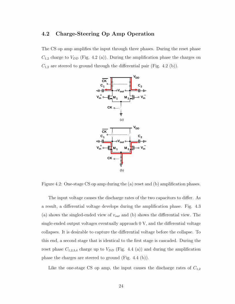
4.2 Charge-Steering Op Amp Operation
The CS op amp amplifies the input through three phases. During the reset phase
C1,2 charge to VDD (Fig. 4.2 (a)). During the amplification phase the charges on
C1,2 are steered to ground through the differential pair (Fig. 4.2 (b)).
VDD
CK
CK
M M1 2
C1 C
Vin Vin
2
VDD
CK
CK
M M1 2
C1 C
Vin Vin
2
Vout
Vout
(a)
(b)
Figure 4.2: One-stage CS op amp during the (a) reset and (b) amplification phases.
The input voltage causes the discharge rates of the two capacitors to differ. As
a result, a differential voltage develops during the amplification phase. Fig. 4.3
(a) shows the singled-ended view of vout and (b) shows the differential view. The
single-ended output voltages eventually approach 0 V, and the differential voltage
collapses. It is desirable to capture the differential voltage before the collapse. To
this end, a second stage that is identical to the first stage is cascaded. During the
reset phase C1,2,3,4 charge up to VDD (Fig. 4.4 (a)) and during the amplification
phase the charges are steered to ground (Fig. 4.4 (b)).
Like the one-stage CS op amp, the input causes the discharge rates of C1,2
24

V
0
VDD
t
Vin,CM
Vth
0t t1 t2
(a)
rese
t
amp
hold
0
V
0
t0t t1 t2
rese
t
amp
hold
0
out out
(b)
Figure 4.3: One-stage CS op amp output vs time in (a) single-ended and (b)
differential views.
VDD
CK
CK
M M1 2
C
Vin Vin
V2
VDD
CK
CK
M M3 4
Vxy V Vpq
C1 CC3 4
VDD
CK
CK
M M1 2
C
Vin Vin
V2
VDD
CK
CK
M M3 4
Vxy V Vpq
C1 CC3 4
(a)
(b)
Figure 4.4: Two-stage CS op amp during the (a) reset and (b) amplification
phases.
25

to differ, generating a differential vxy. This voltage is further amplified by the
same mechanism in the second stage to give vpq (Fig. 4.5). By properly sizing
the transistors and capacitors, the common mode of vx,y falls below the threshold
of M3,4 when the common mode of vp,q falls to about VDD/2. At this point M3,4
turn off, holding the output vpq. Note that M1,2,3,4 remain in saturation during
the amplification phase (from t0 to t1). At t2 vpq is sampled by the next pipelined
stage.
p,qx,y
0
VDD
t
Vin,CM
Vth
0t t1 t2
rese
t
amp
hold
0
0 t
0t t1 t2
rese
t
amp
hold
0
V
0
VDD
t
V
0t t1 t2
out,CM
rese
t
amp
hold
0
V
0 t
0t t1 t2
rese
t
amp
hold
0
V
Vxy pq
(a)
(b)
Figure 4.5: Two-stage CS op amp output vs time in (a) single-ended and (b)
differential views.
Figure 4.7 shows the complete op amp schematic. The addition of two cross-
coupled capacitors CM creates a local positive feedback in the first stage to boost
the open loop gain. The tunable resistor RCM provides the output common mode
control (Chapter 5).
26

VDD
CK
CK
M M1 2
C
Vin Vin
V2
VDD
CK
CK
M M3 4
Vxy V Vpq
C1 CC3 4
Figure 4.6: Two-stage CS op amp during the hold phase.
C
VDD
CK
Vin
VDD
Vout
C1C
M 1 M 2
M M3 4
C2
RCM
C C3 4
CK CK
CK
XY
M
M
Figure 4.7: Charge-steering op amp.
4.3 Charge-Steering Op Amp Gain Analysis
The CS op amp provides signal gain by integrating currents on capacitors. Fig.
4.8 shows the small-signal equivalent half-circuit of the op amp during the ampli-
fication phase.
V ( (t
Cx
V ( (t
Cg ( (tVg Vinm1,2
ro1,2
r( (tm3,4 o3,4 3,4
x,y
x,y
p,q
Figure 4.8: Equivalent half-circuit of the op amp in the amplification phase.
Both differential pairs are in the saturation region. Since the first differential
27

pair is biased at a constant voltage, gm1,2 is a constant. The second differential
pair, however, experiences a shifting bias from VDD at the beginning of the am-
plification phase to 0 at the end of the phase, yielding a time-changing gm3,4(t)
(Fig. 4.9).
0
t0t t1 t2
(a)
rese
t
amp
hold
0
gm ( (t3,4
Figure 4.9: Op amp transconductance versus time.
The value of gm3,4(t) during the amplification phase can be approximated using
a straight line. Assuming t1 − t0 ≪ ro1,2C1,2, ro3,4C3,4, the output voltage vp,q(t)
at t = t1 is
vp,q(t1) =
∫ t1
t0
gm3,4 (t)
C3,4
∫ t
t0
gm1,2
C1,2vindψdt
=1
3
gm1,2
C1,2
gm3,4
C3,4(t1 − t0)
2 vin
(4.1)
Where gm3,4 is the average transconductance of M3,4 during the amplification
phase, hereafter written as gm3,4 for simplicity.
Since the output voltage does not change during the hold mode, vp,q(t2) =
vp,q(t1). Letting ta = t1 − t0, the op amp gain is
A ≡ vp,q(t2)
vin=
1
3
gm1,2
C1,2
gm3,4
C3,4t2a (4.2)
28

If transistor output resistance is considered, the differential equation for a
single stage is:
−gm1,2vin +v1,2(t)
ro1,2+ C1,2
dv1,2(t)
dt= 0 (4.3)
Solving the differential equation and cascading two stages gives the total gain:
A =1
3gm1,2ro1,2
(
1 − exp
(
−taro1,2C1,2
))
gm3,4ro3,4
(
1 − exp
(
−taro3,4C3,4
))
(4.4)
4.4 Charge-Steering Op Amp Noise Analysis
4.4.1 Mathematical Background
This section provides the mathematical background to obtain a noise expression
for the op amp. First, consider a simple circuit that has a current source, a
resistor, and a capacitor (Fig. 4.10)
V ( (t
( (tI R C
Figure 4.10: Noise in an RC circuit
The current source i(t) is a random process that models the noise in the
circuit. The goal is to express the statistical properties of v(t) as a function of the
statistical properties of i(t) and the circuit parameters R and C. The differential
equation for this circuit is
dv(t)
dt=
−1
RCv(t) +
1
Ci(t) (4.5)
29

and the initial condition is
v(0) = vo (4.6)
The solution of (4.5) is
v(t) =
∫ t
0
e−1
RC(t−ψ) 1
Ci(ψ)dψ + voe
−1
RCt (4.7)
A couple of observations of (4.7) provides insight for the circuit. First, the
second term on the right-hand side of (4.7) indicates that the initial voltage vo on
the capacitor decays with a time constant of RC (the natural response). Next,
the first term on the right-hand side of (4.7) shows that the noise current arriving
at time ψ creates a noise voltage equal to i(ψ)dψ/C. This noise voltage also
decays with a time constant of RC, and the amount of time allowed for decaying
is (t− ψ). Finally, the integration of the first term accounts for the effects of all
the noise currents that arrive between time 0 and t (the forced response).
In many realistic scenarios the time interval (defined here as the amount of
time between time zero and the moment of observation) is much smaller than the
circuit’s time constant i.e. t≪ RC. In those cases (4.7) can be simplified to
v(t) =
∫ t
0
1
Ci(ψ)dψ + vo (4.8)
If i(t) is a thermal noise source, it can be expressed as
i(t) = ηξ(t) (4.9)
where η is a constant scaling factor, ξ(t) is a white noise process with a di-
mension of√
Hz [13] and has the following properties
30
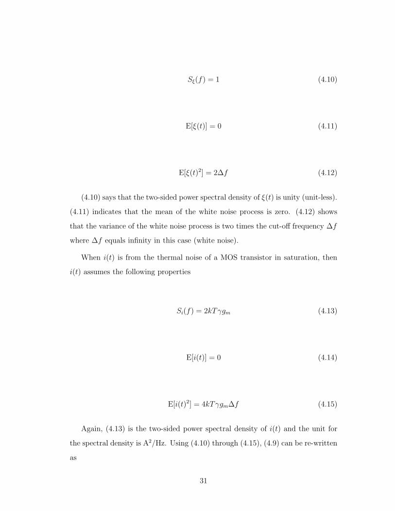
Sξ(f) = 1 (4.10)
E[ξ(t)] = 0 (4.11)
E[ξ(t)2] = 2∆f (4.12)
(4.10) says that the two-sided power spectral density of ξ(t) is unity (unit-less).
(4.11) indicates that the mean of the white noise process is zero. (4.12) shows
that the variance of the white noise process is two times the cut-off frequency ∆f
where ∆f equals infinity in this case (white noise).
When i(t) is from the thermal noise of a MOS transistor in saturation, then
i(t) assumes the following properties
Si(f) = 2kTγgm (4.13)
E[i(t)] = 0 (4.14)
E[i(t)2] = 4kTγgm∆f (4.15)
Again, (4.13) is the two-sided power spectral density of i(t) and the unit for
the spectral density is A2/Hz. Using (4.10) through (4.15), (4.9) can be re-written
as
31

i(t) =√
2kTγgmξ(t) (4.16)
Another useful process for the calculations in this section is the Wiener process
W (t) or Brownian motion. The time derivative of the Wiener process is the white
noise process [14]
dW (t)
dt= ξ(t) (4.17)
Using (4.16) and (4.17) and substituting into (4.7), the equation for the output
voltage v(t) becomes
v(t) =
∫ t
0
e−1
RC(t−ψ) 1
C
√
2kTγgmdW + voe−1
RCt (4.18)
If substituting (4.16) and (4.17) into the simplified equation (4.8) instead, then
v(t) becomes
v(t) =
∫ t
0
1
C
√
2kTγgmdW + vo (4.19)
Equations (4.18) and (4.19) express v(t) as a function of the circuit parameters
and the Wiener process. Because v(t) is a random process, it has statistical
properties i.e. mean and variance. Ito’s integral [13] from stochastic differential
equations provides the suitable relationships to calculate the mean and variance
of v(t). These relationships are
E
[∫ t
0
GdW
]
= 0 (4.20)
32

E
[
(∫ t
0
GdW
)2]
= E
[(∫ t
0
G2dψ
)]
(4.21)
Where G is a function of ψ. Using (4.20) and (4.21), the mean and variance
of v(t) from (4.18) are calculated
E [v(t)] = voe−1
RCt (4.22)
E[
v(t)2]
=kTγgmR
C
(
1 − e−2
RCt)
+ v2oe
−2
RCt (4.23)
=E [i(t)2]R
4C∆f
(
1 − e−2
RCt)
+ v2oe
−2
RCt (4.24)
From the above results some observations are made: First, (4.22) shows that
the initial voltage on the capacitor determines the mean value of v(t). The noise
current source does not contribute to the mean. This mean value decreases with
a time constant of RC as the observation moment t occurs later, and approaches
zero as t→ ∞. Second, the first term in (4.24) shows that the variance increases
as t increases, and approaches a constant value as t→ ∞. Third, the second term
in (4.24) shows that the initial voltage also affects the variance, and this effect
diminishes to zero as t → ∞. Interestingly, if t → ∞ and E [i(t)2] = 4kT∆f/R,
then (4.24) becomes kT/C, which is the expected result if the noise current is
from a resistor that has a value R.
Using the simplified equation (4.19) and (4.20), (4.21), the results become
E [v(t)] = vo (4.25)
33
E[
v(t)2]
=2kTγgmC2
t+ v2o (4.26)
=E [i(t)2]
2C2∆ft+ v2
o (4.27)
(4.25) and (4.27) show that, if the time interval is much smaller than the
circuit’s time constant i.e. t ≪ RC, the mean of v(t) will only depend on the
initial condition, and the variance will increase linearity with the time interval.
4.4.2 Noise in the Reset Phase
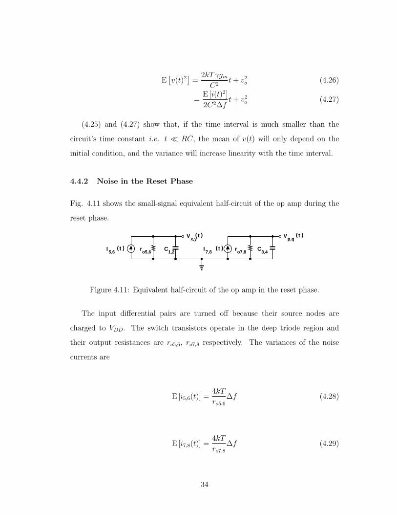
Fig. 4.11 shows the small-signal equivalent half-circuit of the op amp during the
reset phase.
V ( (t
( (tI C
( (t
( (tI Cr r5,6 o5,6 7,8 o7,81,2 3,4
x,yV
p,q
Figure 4.11: Equivalent half-circuit of the op amp in the reset phase.
The input differential pairs are turned off because their source nodes are
charged to VDD. The switch transistors operate in the deep triode region and
their output resistances are ro5,6, ro7,8 respectively. The variances of the noise
currents are
E [i5,6(t)] =4kT
ro5,6∆f (4.28)
E [i7,8(t)] =4kT
ro7,8∆f (4.29)
34
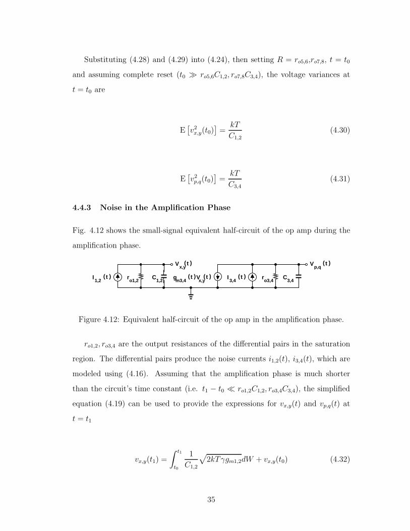
Substituting (4.28) and (4.29) into (4.24), then setting R = ro5,6,ro7,8, t = t0
and assuming complete reset (t0 ≫ ro5,6C1,2, ro7,8C3,4), the voltage variances at
t = t0 are
E[
v2x,y(t0)
]
=kT
C1,2
(4.30)
E[
v2p,q(t0)
]
=kT
C3,4(4.31)
4.4.3 Noise in the Amplification Phase
Fig. 4.12 shows the small-signal equivalent half-circuit of the op amp during the
amplification phase.
V ( (t
( (tI C
V ( (t
( (tI Cg ( (tV1,2
ro1,2
r( (t1,2
x,y
m3,4 x,y 3,4 o3,4 3,4
p,q
Figure 4.12: Equivalent half-circuit of the op amp in the amplification phase.
ro1,2, ro3,4 are the output resistances of the differential pairs in the saturation
region. The differential pairs produce the noise currents i1,2(t), i3,4(t), which are
modeled using (4.16). Assuming that the amplification phase is much shorter
than the circuit’s time constant (i.e. t1 − t0 ≪ ro1,2C1,2, ro3,4C3,4), the simplified
equation (4.19) can be used to provide the expressions for vx,y(t) and vp,q(t) at
t = t1
vx,y(t1) =
∫ t1
t0
1
C1,2
√
2kTγgm1,2dW + vx,y(t0) (4.32)
35
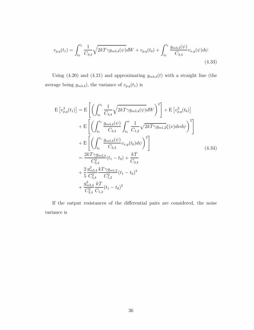
vp,q(t1) =
∫ t1
t0
1
C3,4
√
2kTγgm3,4(ψ)dW + vp,q(t0) +
∫ t1
t0
gm3,4(ψ)
C3,4vx,y(ψ)dψ
(4.33)
Using (4.20) and (4.21) and approximating gm3,4(t) with a straight line (the
average being gm3,4), the variance of vp,q(t1) is
E[
v2p,q(t1)
]
= E
[
(∫ t1
t0
1
C3,4
√
2kTγgm3,4(ψ)dW
)2]
+ E[
v2p,q(t0)
]
+ E
[
(∫ t1
t0
gm3,4(ψ)
C3,4
∫ ψ
t0
1
C1,2
√
2kTγgm1,2ξ(ν)dνdψ
)2]
+ E
[
(∫ t1
t0
gm3,4(ψ)
C3,4vx,y(t0)dψ
)2]
=2kTγgm3,4
C23,4
(t1 − t0) +kT
C3,4
+2
5
g2m3,4
C23,4
kTγgm1,2
C21,2
(t1 − t0)3
+g2m3,4
C23,4
kT
C1,2(t1 − t0)
2
(4.34)
If the output resistances of the differential pairs are considered, the noise
variance is
36
E[
v2p,q(t1)
]
= E
(
A2
∫ ta
0
exp
(
− (ta − t)
r1,2C1,2
)
√
2kTγgm1,2
C1,2dW
)2
+E
[
(
A2vx,y (0) exp
(
−tar1,2C1,2
))2]
+E
(
∫ ta
0
exp
(
− (ta − t)
r3,4C3,4
)
√
2kTγgm3,4
C3,4dW
)2
+E
[
(
vp,q (0) exp
(
−tar3,4C3,4
))2]
=2
5A2
2
kTγgm1,2
C21,2
ro1,2C1,2
2
(
1 − exp
(
−2taro1,2C1,2
))
+ A22
kT
C1,2exp
(
−2taro1,2C1,2
)
+2kTγgm3,4
C23,4
ro3,4C3,4
2
(
1 − exp
(
−2taro3,4C3,4
))
+kT
C3,4
exp
(
−2taro3,4C3,4
)
(4.35)
where A2 is the gain of the output stage
A2 = gm3,4ro3,4
(
1 − e−ta
ro3,4C3,4
)
(4.36)
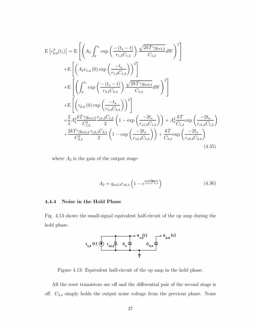
4.4.4 Noise in the Hold Phase
Fig. 4.13 shows the small-signal equivalent half-circuit of the op amp during the
hold phase.
V ( (t
( (tI Cx
V ( (t
Cro1,21,2
x,y
3,4
p,q
Figure 4.13: Equivalent half-circuit of the op amp in the hold phase.
All the reset transistors are off and the differential pair of the second stage is
off. C3,4 simply holds the output noise voltage from the previous phase. Noise
37

coupling from vx,y to vp,q is negligible because Cgd3,4 ≪ C3,4 (C3,4 are the sampling
capacitors from the next pipelined stage). Since no new noise is injected into the
output node, the variance of the output noise voltage at t = t2 remains unchanged
from the end of the previous phase. The differential output-referred noise has twice
the variance. The expression for the differential output-referred noise variance at
the end of the hold phase is
E[
v2pq,diff(t2)
]
=4kTγgm3,4
C23,4
ta +2kT
C3,4+
4
5
g2m3,4
C23,4
kTγgm1,2
C21,2
t3a +2g2
m3,4
C23,4
kT
C1,2t2a (4.37)
If the finite output resistance of the transistor is considered, the differential
output-referred noise voltage variance at the end of the hold phase is
E[
v2pq,diff(ta)
]
=4
5A2
2
kTγgm1,2
C21,2
ro1,2C1,2
2
(
1 − exp
(
−2taro1,2C1,2
))
+ 2A22
kT
C1,2exp
(
−2taro1,2C1,2
)
+4kTγgm3,4
C23,4
ro3,4C3,4
2
(
1 − exp
(
−2taro3,4C3,4
))
+2kT
C3,4exp
(
−2taro3,4C3,4
)
(4.38)
where A2 is the gain of the output stage
A2 = gm3,4ro3,4
(
1 − e−ta
ro3,4C3,4
)
(4.39)
4.4.5 Input-Referred Noise Voltage Variance
Dividing the output noise voltage variance (4.37) by the square of the gain (4.2),
the input-referred noise voltage variance is
E[
v2in,diff(t2)
]
=E[
v2pq,diff(t2)
]
A2
=36kTγC2
x
g2m1,2gm3,4t3a
+18kTC2
xC3,4
g2m1,2g
2m3,4t
4a
+36kTγ
5gm1,2ta+
18kTC1,2
g2m1,2t
2a
(4.40)
38

For completeness, (4.38) divided by the square of (4.4) gives the input-referred
noise voltage variance after accounting for finite transistor output resistance
E[
v2in,diff(t2)
]
=18kTγ
(
1 − e−2ta
ro3,4C3,4
)
g2m1,2gm3,4r2
o1,2ro3,4C3,4
(
1 − e−ta
ro1,2C1,2
)2 (
1 − e−ta
ro3,4C3,4
)2
+18kTe
−2taro3,4C3,4
g2m1,2g
2m3,4r
2o1,2r
2o3,4C3,4
(
1 − e−ta
ro1,2C1,2
)2 (
1 − e−ta
ro3,4C3,4
)2
+18kTγ
(
1 − e−2ta
ro1,2C1,2
)
5gm1,2ro1,2C1,2
(
1 − e−ta
ro1,2C1,2
)2 +18kTe
−2taro1,2C1,2
g2m1,2r
2o1,2C1,2
(
1 − e−ta
ro1,2C1,2
)2
(4.41)
4.4.6 Closed-Loop Op Amp Noise
If the op amp is placed in a closed loop (Fig. 4.14), its open-loop noise voltage vn
will appear at the output vout through the transfer function
voutvn
=
(
1 +Cf
Cin + Cp + CfA
)
−1
(4.42)
Where A is the open-loop gain of the op amp.
Using (4.38) and (4.42), the calculated closed-loop output-referred noise volt-
age variance is 19.0 nV 2, a good agreement with 18.2 nV 2 from simulation
C f
C in
CL
VoutA
Vn
Cp
Figure 4.14: Op amp noise in closed-loop.
39

4.5 Closed-Loop Charge-Steering Op Amp
4.5.1 Overview
The charge-steering op amp is placed in a closed-loop configuration to form an
MDAC as shown in Fig. 4.15
C
1
2
C
V
f
C
C C1
2
L
L
C f
V
V
in
φ
φ
φ
φ
Vout
in
in
REFKV
REFKV
φ1
φ1
VG
VG
φ3
φ1
φ
φ
2
3
TCK
Res
et
Sam
ple
Am
plify
Com
p &
Ref
Figure 4.15: Closed-loop op amp.
During the reset phase the op amp’s sampling capacitors are connected to the
input vin and the virtual ground reset voltage VV G. The internal nodes of the
op amp and the output vout are reset to VDD. In the sample phase the op amp
samples the input on the capacitors Cin. In the next phase the comparators (not
shown) make decisions and connect Cin to ±KVREF , and the op amp waits for
the voltages to settle. Finally, during the amplify phase the op amp amplifies the
input and the output is held on CL.
4.5.2 Closed-Loop Model
The closed-loop behavior of the CS op amp presents interesting and useful prop-
erties. The simplified model is shown in Fig. 4.16. The transfer function of the
closed-loop CS op amp is (4.43) and its poles are located at (4.44)
40

C
CVxVx
inV outVin
1
outV
Op Amp
C
g 3,4m
t
3,4
t
(a) (b)
f
Figure 4.16: (a) Model of the closed-loop CS op amp and (b) its step response.
VoutVin
=−Cin
Cin + CM
gm1,2gm3,4
s2C1,2CL + gm1,2gm3,4β(4.43)
sp = ±j√
gm1,2gm3,4
C1,2CLβ (4.44)
Because the poles are on the imaginary axis, the system is marginally stable.
Fortunately, after accounting for transistor output resistances the poles move into
the left-half plane, and the closed-loop op amp becomes an underdamped second-
order system. The step response is shown in Fig. 4.16 (b). Because the first
stage shuts the second stage off at t = t1, it is possible for the output to “freeze”
at a voltage level that is higher than the final settled level. This gain boost
allows the closed-loop gain to be equal or slightly greater than the capacitor ratio
Cin/Cf , even in the presence of finite open-loop gain and op amp input parasitic
capacitance - an advantage that the conventional op amp topologies do not offer.
4.6 Op Amp Comparison
The CS op amp is compared to the conventional one-stage and two-stage op amps,
which are shown in Fig. 4.17 and Fig. 4.18 respectively. The op amps are placed
in a closed-loop configuration, as shown in Fig. 4.19
41
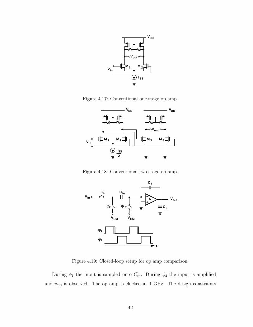
VDD
M M1 2
I SS
Vout
Vin
Figure 4.17: Conventional one-stage op amp.
VDD
M M1 2
I SS
VDD
M M
Vout
Vin3 4
2
Figure 4.18: Conventional two-stage op amp.
1φ
φ
VoutVin A
φ1E2
C in
C
VCM VCM
CL
t
1φ
φ2
f
Figure 4.19: Closed-loop setup for op amp comparison.
During φ1 the input is sampled onto Cin. During φ2 the input is amplified
and vout is observed. The op amp is clocked at 1 GHz. The design constraints
42

are: VDD = 1 V, Power = 2.5 mW, A = 10 V/V, Vout = 0.6 Vpp, CL = 250 fF,
Cin = 480 fF, and Cf = 240 fF. The performances of the op amps are shown in
Table 4.1.
Table 4.1: Op amp performance comparison.
1 Stage 2 Stage CS Amp
SDR 48 dB 53 dB 54 dB
τSettling Time (3 )
67 nV 2 2138 nV 265 nVIP Ref. Noise Pwr.
560 ps 370 ps 80 ps
As the table shows, the CS op amp achieves more than fourfold increase in
speed, twofold reduction in noise, and comparable signal-to-distortion ratio (SDR)
as the two-stage design under the same constraints. Figure 4.20 shows the sim-
ulated step response of the three closed-loop op amps. The sharp rising edge of
the CS op amp clearly demonstrates its speed superiority over the conventional
op amps.
2.5 3 3.5 4 4.5−0.1
0
0.1
0.2
0.3
0.4
0.5
0.6
0.7
Time (ns)
Vou
t (V
)
CS Amp
1−Stage Amp
2−Stage Amp
Figure 4.20: Op amp step response comparison.
43

CHAPTER 5
Prototype ADC Design
5.1 ADC Architecture
The speed of a pipelined ADC is set by the speed of its stages, particularly the first
few. For high speed designs, the feedback factor of the op amp must be maximized,
leading to small closed-loop gains and a small number of bits resolved per stage.
The prototype ADC resolves 1.5-bits per stage to maximize its speed. As was
discussed in Chapter 3, the 1.5-bit topology provides tolerances to comparator
offsets. However, this topology still suffers from other errors that cause the the
output to saturate, resulting in the loss of signal information. Saturation occurs
near the minimum and maximum values in the input range. Typical designs reduce
the input amplitude and/or amplify the residue by less than the nominal factor
to avoid signal saturation. However, reducing the input amplitude decreases the
dynamic range, and using a smaller residue gain increases the input-referred noise.
To avoid signal saturation and to improve linearity, two extra comparators are
added to the first stage to fold the ends of the input-output transfer characteristic
toward the center, reducing the output range [15]. Figure 5.1 (a) shows the transfer
characteristic of a 1.5-bit stage (solid line) and after adding two extra comparators
(dotted line). Figure 5.1 (b) shows the characteristics of a 2.5-bit (folded) stage.
Table 5.1 summarizes the topology parameters and provides comparisons.
The folded topologies reduce the output swing by half, avoiding signal satura-
tion and improving linearity at the cost of extra comparators and MDAC/comparator
44

VREF
VREF
VREFVREF
VREF
VREF
VREFVREF
(a) (b)
Figure 5.1: Input-output characteristic of (a) 1.5-bit and (b) 2.5-bit topologies.
1.5-b 1.5-b folded 2.5-b 2.5-b folded
Stage Gain (V/V) 2 2 2 2
Max Output Swing (±VREF ) 1 12
12
14
MDAC Ref. (±VREF ) 04, 1
404, 1
4, 2
408, 1
8, 2
8, 3
808, 1
8, 2
8, 3
8, 4
8
Comparator Ref. (±VREF ) 18
18, 3
8116
, 316
, 516
116
, 316
, 516
, 716
Table 5.1: Stage topology parameters and comparison.
reference levels. The 2.5-bit topologies offer smaller output swings than the 1.5-
bit designs, but require more reference levels, which usually come from a power-
hungry resistor ladder. On the other hand, the smaller number of reference levels
in the 1.5-bit topologies can be generated by a power-efficient capacitive divider.
For this reason the 1.5-bit folded topology is chosen for the first stage in the pro-
totype. Figure 5.2 shows the detailed input-output transfer characteristic for the
1.5-bit folded stage. Note that the correction range of the 1.5-bit folded topology
remains the same as that of the 1.5-bit topology. Because the swing is reduced by
half after the first stage, the remaining stages can use the typical 1.5-bit topology.
The prototype ADC consists of twelve 1.5-bit pipelined stages and a final 1-
bit flash stage (Fig. 5.3). Although the ADC is 10-bit, the above design provides
13 physical bits. The three additional bits are used to suppress quantization
errors during calibration and truncated during normal operation. The G(·) and
45

VREF
VREF
VR
EF
VR
EF
Vin
Vout
/V 2
REF /V 2
RE
F/
V4
RE
F/
V4 0
0
REF
RE
F/
V4
3
RE
F/
V4
3
Figure 5.2: Stage 1 input-output transfer characteristic.
H(·) blocks implement the digital calibration, which is explained in the following
section.
2 2 2 2
DA
C
AD
C
DA
C
1.5b
( )G2( )G1
( )H 1 ( )H 2
Vin
Dout
AD
C
DA
C
1.5b
( )G3
( )H 3
AD
C
DA
C
1.5b
( )G
( )H
( )G
1b AD
C
12 13
Stage 1 Stage 12
12
AD
C1.
5b fo
ld
Figure 5.3: Proposed ADC architecture.
46

5.2 Calibration
5.2.1 Overview
ADC calibration removes the errors from the ADC’s input-output transfer char-
acteristic. Calibration can be categorized into three main types — analog calibra-
tion, digital calibration, and mixed-signal calibration. Analog calibration adjusts
analog “tuning knobs”, which are redundant analog circuits, to remove the errors
(Fig. 5.4 (a)). Digital calibration keeps the analog circuits intact and adds a dig-
ital processing block to remove the errors (Fig. 5.4 (b)). Mixed-signal calibration
uses a combination of analog and digital circuits to remove the errors (Fig. 5.4
(c)).
Analog DigitalVin Dout
Redun−dancy
Analog DigitalVin Dout
Redun−dancy
Analog DigitalVin Dout
Redun−dancy
(a) (b) (c)
Figure 5.4: ADC calibration using (a) analog only, (b) digital only, and (c)
mixed-signal techniques.
Digital calibration has become increasing popular due to the benefits of pro-
cess scaling. However, digital calibration is unable to correct certain types of
errors that involve the loss of analog information. For example, when an op
amp saturates the analog information is lost, and no amount of digital processing
can recover that lost information. Therefore, a mixed-signal approach is attrac-
tive to both preserve and condition signal information to achieve a higher ADC
performance. This work adopts a mixed-signal calibration by using redundant
comparators and digital correction functions to improve the ADC’s accuracy.
47

5.2.2 Proposed Foreground Calibration
This work utilizes the foreground calibration technique from [16]. The basic idea
is to build a digital processing block that will convert the un-calibrated output to
a calibrated one that more accurately represents the input (Fig. 5.5).
Vin ADCDout,calDout,uncal
Dout,cal
Vin
D
Vin
out,uncal
DigitalProc.
Figure 5.5: Digital calibration of ADC.
The G(·) function in Fig. 5.3 corrects DAC errors and the H(·) function
corrects op amp errors. This calibration technique is attractive as it allows the
use of low-gain, low-power, and high-speed op amps in the ADC. Also, the digital
circuits that implement the polynomials become more power and area-efficient as
process technology scales down. Finally, the high-precision calibration voltages
generated from a resistor ladder will also benefit from the improved matching of
passive elements in a scaled technology.
The calibration proceeds as follows: First, the calibration engine sweeps Stage
5’s input with high-precision voltages from a calibration DAC (Fig. 5.6). Then,
the G(·) and H(·) functions convert the stages’ output to Dout. A least-mean-
squares (LMS) engine uses the error between Dcal and Dout to tune the coefficients
of G(·) and H(·) until the error is minimized. Once Stages 5-13 are calibrated,
they form an ideal backend ADC to calibrate the succeeding stages. Figure 5.7
shows the calibration of Stage 4, where the same procedure is repeated.
The calibration proceeds stage-by-stage in this fashion until Stage 1 is cali-
brated. However, special attention must be paid during the calibration of Stages
48
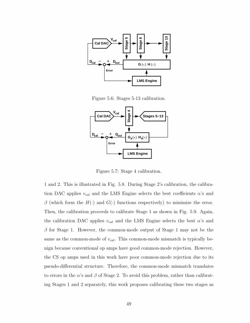
Sta
ge 5
Sta
ge 1
3
Sta
ge 6
( )G ( )H
LMS Engine
DoutDcal
Cal DACVcal
Error
Figure 5.6: Stages 5-13 calibration.
( )G ( )H
LMS Engine
DoutDcal
Cal DACVcal
Error
Sta
ge 4
Stages 5−13
4 4
Figure 5.7: Stage 4 calibration.
1 and 2. This is illustrated in Fig. 5.8. During Stage 2’s calibration, the calibra-
tion DAC applies vcal and the LMS Engine selects the best coefficients α’s and
β (which form the H(·) and G(·) functions respectively) to minimize the error.
Then, the calibration proceeds to calibrate Stage 1 as shown in Fig. 5.9. Again,
the calibration DAC applies vcal and the LMS Engine selects the best α’s and
β for Stage 1. However, the common-mode output of Stage 1 may not be the
same as the common-mode of vcal. This common-mode mismatch is typically be-
nign because conventional op amps have good common-mode rejection. However,
the CS op amps used in this work have poor common-mode rejection due to its
pseudo-differential structure. Therefore, the common-mode mismatch translates
to errors in the α’s and β of Stage 2. To avoid this problem, rather than calibrat-
ing Stages 1 and 2 separately, this work proposes calibrating these two stages as
49

one block. Figure 5.10 illustrates this technique.
Vcal
α x1 α x 22 α x 3
3
Stage 1
β
Stage 2
Error
Dcal
Stages 3−13
Figure 5.8: Stage 2 calibration.
Vcal
α x1 α x 22 α x 3
3α x1 α x 22 α x 3
3
Stage 1
β β
Stage 2
Dcal
Error
Stages 3−13
Figure 5.9: Stage 1 calibration.
The calibration applies vcal to Stage 1 and the LMS Engine simultaneously
selects the best α’s and β for both Stage 1 and 2. In this way, the common
mode between the two stages is encapsulated in the combined block and does
not affect the selection of the coefficients. It is worth noting that the remaining
stages do not have the common-mode mismatch issue because of the common-
mode rejection MDAC topology used (the MDAC topologies will be discussed
later in this chapter).
Another issue with using a resistive calibration DAC is the slow settling of
50

Vcal
α x1 α x 22 α x 3
3α x1 α x 22 α x 3
3
Stage 1
β β
Stage 2
Error
Dcal
Stages 3−13
Figure 5.10: Calibration of Stages 1, 2 as one block.
vcal. Shown in Fig. 5.11 is the calibration voltage path.
VoutA
C
CM
V incal
Figure 5.11: Calibration voltage path.
Due to the 31 taps required to generate the different levels of vcal, the total
associated parasitic capacitances of the switches is large. The resulting time con-
stant of the calibration path prevents vcal from full settling during the sampling
phase. Slowing down the clock during calibration will allow vcal to settle, but the
mismatch between the dynamic characteristics of the ADC at slow and full clock
rates introduces coefficient errors [16]. This work proposes a new clock gating
technique to resolve this issue (Fig. 5.12).
The idea of clock gating is to generate a clock waveform that contains a long
sampling phase to allow vcal to settle, followed by full-rate phases to preserve
51

settlesCKG V
sensed
t
CK
CK
T
cal
CK 16VoutA
C in
C
CKG
Vcal
Vout
CKG
VREFK
f
Figure 5.12: Full-speed calibration by gated clock.
the ADC’s dynamic characteristics. Figure 5.12 shows a full-rate clock CK and
its divided-by-16 version, CK/16. The divided clock gates the full-rate clock
to produce the gated clock CKG, which controls the MDAC’s switches. During
the extended sampling phase, vcal has sufficient time to settle fully. The full-rate
phases follow immediately. Figure. 5.13 shows the simulated vcal settling. Thanks
to the extended sampling phase, vcal reaches its final value of 120 mV. Had clock
gating not been used, vcal would have settled somewhere lower than this value,
resulting in calibration errors.
A third issue with the calibration is the charge injection of the sampling switch
of Stage 1. Figure 5.14 illustrates this problem. At the sampling instant, the
bottom-plate sampling switch injects charges into the op amp’s input node. The
amount of the injected charges is a function of the impedance seen by the switch.
Conventional op amps, due to their good common-mode rejection, is relatively
immune to the injected charges, since the charges are signal-independent and
common to the differential circuit. However in the case of the CS op amp, which
has poor common-mode rejection, the injected charges change the ADC’s char-
acteristic, resulting in calibration inaccuracy. To create equal source impedance
between the two paths, a series resistor Rs/2 is inserted in the calibration path to
mimic the source resistance of the input path (which includes the signal genera-
52

5 10 15
0
20
40
60
80
100
120
140
Time (ns)
Vca
l (m
V)
Figure 5.13: Simulated settling of calibration voltage.
tor’s source resistance and the on-chip termination resistance). A 2-pF capacitor
Cbig mimics the ideal voltage source. By this technique the sampling switch charge
injection in the calibration mode and the operation mode is consistent, giving a
better calibration accuracy.
A
V
V
C in
C
cal
VCM
C
Rs 2
big
Vin
R
Rs
s
out
f
Figure 5.14: Charge injection of the sampling switch.
53

5.2.3 Proposed Background Calibration
During normal operation the ADC may experience temperature and supply varia-
tions. Such environmental changes deviate the ADC’s input-output characteristic
from the one described by the calibration coefficients, degrading the ADC’s per-
formance. Hence, it is desirable to continuously monitor the ADC’s characteristic
and adjust the calibration coefficients to compensate for the drifts. To study the
effect of temperature, the simulated Stage 1 input-output transfer characteristics
at 27 and 60 C are shown in Fig. 5.15.
−600 −400 −200 0 200 400 600−300
−200
−100
0
100
200
300
Vin (mV)
Vou
t (m
V)
27 deg
60 deg
Figure 5.15: Stage 1 input-output characteristics at 27 and 60 C.
The two characteristic curves in Fig. 5.15 are very close to each other, making
it difficult to see the effect of temperature. Therefore, the difference between the
two curves is plotted instead (Fig. 5.16).
From Fig. 5.16, it is evident that the dominant characteristic change is in the
DAC coefficient β, as indicated by the four vertical jumps. The s-shaped segments
come from the change in the third-order nonlinearity coefficient α3. Interestingly,
the gain coefficient α1 sees no appreciable change. From this result, it is proposed
54
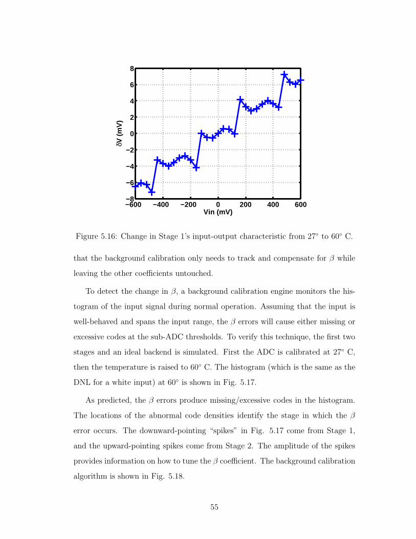
−600 −400 −200 0 200 400 600−8
−6
−4
−2
0
2
4
6
8
Vin (mV)
δV (
mV
)
Figure 5.16: Change in Stage 1’s input-output characteristic from 27 to 60 C.
that the background calibration only needs to track and compensate for β while
leaving the other coefficients untouched.
To detect the change in β, a background calibration engine monitors the his-
togram of the input signal during normal operation. Assuming that the input is
well-behaved and spans the input range, the β errors will cause either missing or
excessive codes at the sub-ADC thresholds. To verify this technique, the first two
stages and an ideal backend is simulated. First the ADC is calibrated at 27 C,
then the temperature is raised to 60 C. The histogram (which is the same as the
DNL for a white input) at 60 is shown in Fig. 5.17.
As predicted, the β errors produce missing/excessive codes in the histogram.
The locations of the abnormal code densities identify the stage in which the β
error occurs. The downward-pointing “spikes” in Fig. 5.17 come from Stage 1,
and the upward-pointing spikes come from Stage 2. The amplitude of the spikes
provides information on how to tune the β coefficient. The background calibration
algorithm is shown in Fig. 5.18.
55

0 200 400 600 800 1000
−1
−0.5
0
0.5
1
Code
DN
L (L
SB
)
Before Calibration
Figure 5.17: ADC output histogram at 60C.
Set th ref εBin Bin
Aquire Samples
No
Yes
βDecrease
βIncrease
Yes
No
Nth −N εref
Nth
N ?ref
Figure 5.18: Background calibration procedure.
First, the calibration engine specifies the locations of the threshold bins Binth
(located at the sub-ADC thresholds), reference bins Binref (bins next to Binth’s),
56

and the error tolerance ǫ. Then, the ADC acquires samples during its normal
operation. The engine compares the number of code counts in the threshold bins
Nth and the reference bins Nref . If the difference is less than ǫ, the current β is
valid, and no tuning is necessary. If the difference is more than ǫ, the engine tunes
β according the relative code counts. Figure 5.19 shows the DNL and INL before
and after the background calibration. The calibration engine effectively removes
the spikes in the histogram and the simulated SDR improved from 54 dB to 68
dB.
0 500 1000
−1
−0.5
0
0.5
1
Code
DN
L (L
SB
)
Before Calibration
0 500 1000−2
−1
0
1
2
Code
INL
(LS
B)
Before Calibration
0 500 1000−1
−0.5
0
0.5
1
Code
DN
L (L
SB
)
After Calibration
0 500 1000−2
−1
0
1
2
Code
INL
(LS
B)
After Calibration
Figure 5.19: DNL and INL before and after background calibration for tempera-
ture compensation.
Supply variation can be similarly compensated by the same algorithm. Figure
5.20 shows the change in Stage 1’s input-output characteristic when it is calibrated
at VDD = 1 V, followed by the supply raised to 1.01 V.
Unlike temperature, supply variation mainly affects the α1 coefficient while
57

−600 −400 −200 0 200 400 600−8
−6
−4
−2
0
2
4
6
8
Vin (mV)
δV (
mV
)
Figure 5.20: Change in Stage 1’s input-output characteristic from VDD = 1.00 V
to 1.01 V.
leaving α3 and β relatively unchanged. Fortunately, α1 errors can be treated as
β errors using the same background algorithm, since the segments in Fig. 5.20
can be properly “stiched” back together to form a linear line by adjusting β. This
allows both the temperature and supply calibrations to run together as one loop.
Figure 5.21 shows the DNL and INL before and after background calibration. The
calibration engine effectively removes the spikes in the DNL and the simulated
SDR improved from 45 dB to 63 dB.
5.3 Proposed Common-Mode Feedback
The CS op amp contains a digitally tunable tail resistor RCM to control its output
common mode (Fig. 5.22). Increasing the resistance of RCM increases the common
mode and vice versa. The conventional method to control the common mode in a
discrete-time system is to use switched capacitors to sense the common mode, then
58

0 500 1000−0.5
0
0.5
1
Code
DN
L (L
SB
)
Before Calibration
0 500 1000−4
−2
0
2
4
Code
INL
(LS
B)
Before Calibration
0 500 1000−0.5
0
0.5
1
Code
DN
L (L
SB
)
After Calibration
0 500 1000−4
−2
0
2
4
Code
INL
(LS
B)
After Calibration
Figure 5.21: DNL and INL before and after background calibration for supply
compensation.
compare the common mode to a reference CMREF and feed back the difference to
the tuning element. However, the sensing capacitors and the comparator decrease
the speed of the op amp and increase the power consumption. To avoid these
penalties, this work proposes a digital common-mode control technique. This
technique merges the common-mode control loop with the existing calibration
loop (Fig. 5.23).
RCM
CK
Vout
ACMREF
Figure 5.22: Conventional common-mode control.
59

CMctrl CMctrl
α x1 α x 22 α x 3
3α x1 α x 22 α x 3
3
Stage 1
β β
Stage 2
Dcal
LMS
Error
Stages 3−13
Figure 5.23: Proposed common-mode control.
This common-mode control technique was conceived by making the follow-
ing observation: When an op amp’s common mode is properly set, its swing is
maximized, and the linearity is maximized. Therefore, the common-mode control
can use linearity as a feedback signal to properly set the tuning element. In this
design, the linearity of the op amp can be detected by looking at the error term
during calibration. By tuning not only the α and β coefficients but also CMctrl,
the LMS Engine finds a combination that minimizes the error term. When the
error term is minimized, the op amp’s common mode is properly set. This im-
plicit common mode sensing obviates the need of explicit sensing elements and
comparators, saving precious power and maximizing the op amp’s speed.
5.4 Circuit Building Blocks
5.4.1 Stage 1
The ADC uses separate MDAC and sub-ADC sampling networks to sample the
input, avoiding a power-hungry master sample-and-hold (Fig. 5.24, single-ended
version shown for simplicity). In the absence of a master sample-and-hold, the
mismatch between the MDAC’s sampling network and the sub-ADC’s sampling
network leads to different sampled values. When the input is close to one of
60

the comparators’ thresholds, this mismatch may cause the sub-ADC to make an
erroneous decision, the equivalent of having a comparator offset (Chapter 3). For-
tunately, the 1.5-bit/stage redundancy corrects this offset digitally. Nevertheless,
the offset increases the output swing of the op amp, introducing higher op amp
nonlinearity and decreasing the SNDR. Therefore, it is desirable to minimize the
mismatch between the two sampling networks. In this ADC, Stage 1 uses 480-fF
Cin. The sampling capacitors of the sub-ADC are scaled down by a factor of
ten from their counterparts in the MDAC to conserve power. To maintain the
same sampling time constant, the sub-ADC’s sampling switch transistor widths
are scaled up by the same factor. Both sampling networks share the same boost-
rapped clocks.
Fig. 5.24 shows Stage 1’s timing diagram. The cycle begins when φ1 goes high,
sampling the input on the capacitors. The input is frozen on the capacitors when
φ1 goes low (bottom-plate sampled by the early edge φ1E). Next, φ2 goes high to
present the input to the comparators. After the voltages at the comparator inputs
settle, the late clock φ2L latches the comparators. The comparator decisions D0−3
pass through some decoder logic (not shown) and activate via φR the MDAC’s
reference switches. The MDAC waits for the reference voltages to settle, after
which φ3 clocks the op amp. The op amp is reset during the sampling, comparison,
and reference settling phases.
5.4.2 Stage 2
Starting from Stage 2, the MDAC and the sub-ADC see the preceding stage’s op
amp output, which settles to a DC value. Therefore, a slight mismatch between
the sampling networks of the MDAC and the sub-ADC would still yield the same
sampled values. To leverage this relaxed matching requirement, the sub-ADC
pre-charges its sampling capacitors during φ2, allowing the comparators to be
latched at the early edge φ1E, resulting in zero dead-time between the sampling
61

C f
C in1φ
φ
VoutVin
REFKV
A
φ
C in1φ
2φ
REF
VVG
VVG
φ
81 V
1φ
2φ
REFVVG
φ
8V
1φ
2φ
REFVVG
φ
8V
1φ
REFVVG
φ
8V
3
5
7
101
C in101
C in101
C in101
MDAC Sampling Network
Sub−ADC Sampling Network
D0
D1
D2
D3
φ3
φ
φ
φ
φ2φ
φ1
φ3
TCK
φ2
φ
Ref
Am
plify
Reset
Com
p
Amplifier
Sam
ple
SamplingNetworks
1E
1E
1E
1E
1E
RR
2L
2L
2L
2L
Figure 5.24: Stage 1 design.
and comparison phases. This is in contrast to stage 1’s timing, where the MDAC
and the sub-ADC sampling networks must operate on the same phases, and a
deadtime between the sampling and comparison phases results. The timing budget
62

allocates approximately 25% of the clock period for reset, 25% for sampling, 25%
for comparison and reference settling, and 25% for amplification. Cin is scaled
down by a factor of two from stage 1 to 240 fF. The sub-ADC uses 30-fF sampling
capacitors to reduce power consumption.
81
1
C f
C in1φ
VoutVin
REFKV
A
φ
C in1φ
2φ
REF
VVG
V8
V
1φ
2φ
REFV
8V
C in
MDAC Sampling Network
Sub−ADC Sampling Network
D0
D1
3
5
8
2φ
2φ
CM
CM
φ3
φ3
TCK
φ2
φ
Am
plify
φ
φ
φ
Amplifier
NetworkSampling
MDAC
NetworkSampling
Pre
char
ge
Res
et
Sam
ple C
omp
R 1E
1E
1E
R
φ1
Sub−ADC
Ref
Figure 5.25: Stage 2 design.
5.4.3 Stage 3
The charge-steering op amp has poor common-mode rejection due to its pseudo-
differential topology. Left unchecked, the common-mode deviation will propagate
from one pipelined stage to the next, shifting op amps out of their optimal bias
points and possibly cause op amp saturation. The common-mode problem is
63
further exacerbated in this ADC because the ADC requires precise calibration of
each stage using a calibration ladder, whose common-mode is not guaranteed to
be the same as that of the stage’s preceding op amp.
To avoid these common-mode problems, starting in Stage 3 the MDAC uses a
fully-differential sampling network to stop the common-mode input from reaching
the op amp. Fig. 5.26 shows the design of Stage 3. The timing diagram is
identical to that of Stage 2. However, the MDAC’s input capacitor now switches
to the common-mode input Vin,CM during φ2. Vin,CM is easily obtained in a
differential circuit by shorting the top plates of the two input capacitors. Using
this technique, the op amp sees only the differential input while rejecting the
common-mode input. The downside to this fully-differential sampling network is
the need of an additional capacitor Cref for reference voltage addition/subtraction.
Cref reduces the op amp’s feedback factor and increases the sampling noise. To
suppress the increased noise, all capacitors and transistor widths in stage 3 are
20% bigger (Cin = 145 fF, scaled down from Stage 2 by a factor of 1.66 instead
of 2), incurring the same proportional power penalty. However, since this power
penalty happens in the smaller stages (3-12), the overall analog power penalty is
reduced to less than 9% - the very reason Stages 1, 2 did not use fully-differential
sampling networks.
5.4.4 Backend Stages
The backend stages (Stages 4-12) use the same topology as Stage 3. Stage 4 is
scaled down by a factor of two from Stage 3 (Cin = 72 fF), and again in Stage 5
(Cin = 36 fF). Due to the diminishing returns in power savings (parasitics start to
dominate), Stages 6 to 12 remain the same size as Stage 5. The final stage (Stage
13) is a 1-bit flash.
64

1
1
C f
C in1φ
2φ
VoutVin A
φ
C in1φ
2φ
REF
VVG
V
φ
8V
1φ
2φ
REFV
φ
8V
C in
MDAC Sampling Network
Sub−ADC Sampling Network
D0
D1
3
5
REFKV
Vin,CM
Cref1φ
φ
V
CM
CM
REF,CM
2
2
5
5
φ3
φ
φ
φ3
TCK
φ2
φ
Am
plify
Amplifier
NetworkSampling
MDAC
NetworkSampling
Pre
char
ge
Res
et
Sam
ple C
omp
R
φ1
Sub−ADC
Ref
R
1E
1E
1E
Figure 5.26: Stage 3 design.
5.4.5 Reference Generation
Stage 1’s MDAC has five reference levels for voltage addition/subtraction. The
subsequent stages’ MDACs each has three reference levels. A straightforward way
to generate the reference levels is to use a resistor ladder. However, the resistor
ladder must be low-resistance to achieve fast settling, leading to high power con-
sumption. This ADC avoids the power-hungry ladder by using capacitive dividers
for reference generation. The capacitive divider is constructed by splitting the
65

input capacitor Cin of the MDAC into several unit capacitors. Each unit capac-
itor connects either to the positive reference +KVREF or the negative reference
−KVREF (Fig. 5.27). The capacitive divider generates the reference levels by
switching different numbers of unit capacitors to +KVREF/−KVREF . Similarly,
the MDACs in Stage 3-12 split the reference capaictor Cref and connect different
numbers of the unit capacitors to +KVREF/−KVREF . The comparator reference
levels are generated by the same fashion. Using this method, the ADC generates
multiple reference levels without a power-hungry resistor ladder. Large on-chip
decoupling capacitors (2 nF between positive and negative reference supplies, and
1 nF each to ground) ensure that the switching transients introduce less than 1
LSB error.
C f
V
φ
A
12
VREF
1φ φ φ
12
VREF
Vin
1E
C inVGR R
Figure 5.27: Stage 1 MDAC reference generation.
5.4.6 Bootstrapping Circuit
The sampling networks use bootstrapping circuits to realize high-speed and highly-
linear switches. The bootstrapping circuit generates a large and constant VGS for
a switch transistor during the ON phase, and 0 VGS during the OFF phase, all at
the same time avoiding more than VDD between any two junctions in the circuit.
Fig. 5.28 shows the schematic of the bootstrapping circuit [17].
M1 is the bootstrapped switch. During the OFF phase CK is low and M5, M6
66
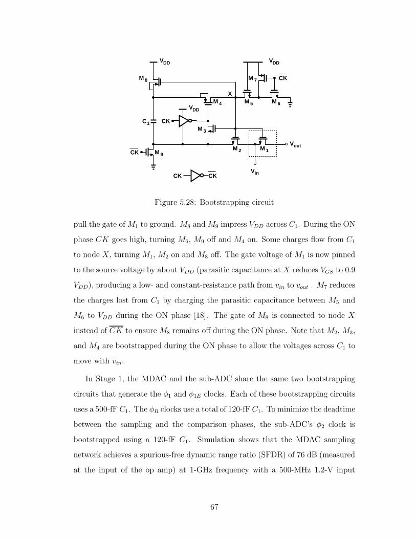
M
VDD
M
M M 1
M
VDD
CK
CK
M
CK M
M
VDD
M
CK CK
2
3
4 5 6
78
9
Vin
Vout
C1
X
Figure 5.28: Bootstrapping circuit
pull the gate of M1 to ground. M8 and M9 impress VDD across C1. During the ON
phase CK goes high, turning M6, M9 off and M4 on. Some charges flow from C1
to node X, turning M1, M2 on and M8 off. The gate voltage of M1 is now pinned
to the source voltage by about VDD (parasitic capacitance at X reduces VGS to 0.9
VDD), producing a low- and constant-resistance path from vin to vout . M7 reduces
the charges lost from C1 by charging the parasitic capacitance between M5 and
M6 to VDD during the ON phase [18]. The gate of M8 is connected to node X
instead of CK to ensure M8 remains off during the ON phase. Note that M2, M3,
and M4 are bootstrapped during the ON phase to allow the voltages across C1 to
move with vin.
In Stage 1, the MDAC and the sub-ADC share the same two bootstrapping
circuits that generate the φ1 and φ1E clocks. Each of these bootstrapping circuits
uses a 500-fF C1. The φR clocks use a total of 120-fFC1. To minimize the deadtime
between the sampling and the comparison phases, the sub-ADC’s φ2 clock is
bootstrapped using a 120-fF C1. Simulation shows that the MDAC sampling
network achieves a spurious-free dynamic range ratio (SFDR) of 76 dB (measured
at the input of the op amp) at 1-GHz frequency with a 500-MHz 1.2-V input
67

sinusoid – sufficient for a 10-bit ADC.
5.4.7 Comparator
The comparators in each pipelined stage form a sub-ADC that quantizes the
stage’s input and provides digital controls signals for the MDAC. The comparison
time must be short to achieve a high overall ADC speed. This ADC uses the
StrongARM comparator topology (Fig 5.29) for high-speed, low-power operation
[19].
VDD
VoutVout
Vin Vin
CK
CK CK
M M1 2
M T
M 3
M
M
M
4
5 6
Figure 5.29: Comparator
When CK is low, the comparator outputs are reset to VDD. When CK goes
high, the differential pair M1, M2 turn on, discharging the parasitic capacitors
at the drain nodes. As the drain voltages fall, M3 and M4 turn on and begin
to discharge the output nodes. The differential input causes the discharge rates
between the output nodes to differ, and the positive feedback provided by M4−6
amplifies this difference to full rail voltages.
5.4.8 Calibration DAC
The calibration DAC provides high-precision voltages to the ADC during calibra-
tion. Figure 5.30 shows the layout of the DAC [16]. The DAC is a continuous
silicided polysilicon resistor with 31 taps at the edge. The unit resistance is 5 Ω
68

and the linearity is 12-bit. The DAC is turned off after calibration to save power.
µ m
µ m
20
V1 V2 V V3130
240
Calibration DAC
Figure 5.30: Calibration DAC layout.
5.4.9 Clock Generator
The ADC requires multiple non-overlapping clock phases for proper operation.
Fig. 5.31 shows a block diagram of a conventional multi-phase clock generator
[20, 21].
VDD
Vin Vin VoutVout
VDD VDD
4 4 mComb.Logic
Non−Overlap2CML−to−
CMOSVin
22
CK2CK CK CK
Figure 5.31: Conventional clock generator.
The clock generator takes a differential current-mode-logic (CML) input from
off-chip and converts it to CMOS levels. Then, a divider divides down the clock to
69

generate quadrature phases. The non-overlap generator inserts non-overlapping
time between the four phases. Finally, the combinational logic uses the four phases
to create 25%, 50%, and 75% duty-cycle clocks for the ADC.
Several issues plague the conventional clock generator: First, at high clock
rates, it is not trivial to generate differential signals from off-chip and ensure
small phase imbalance after going through bond wires. Second, the non-overlap
generator (Fig. 5.32) creates overly conservative non-overlap time, reducing the
time available for circuit operations. Third, the critical sampling clock edge (Stage
1’s sampling edge) must pass through the entire clock generator chain, thus suf-
fering from a sever power-noise trade-off. To address these problems, a new clock
generator is proposed (Fig. 5.33).
Vin
VinVout
Vout
Figure 5.32: Conventional non-overlap generator.
4 4 m
1
Comb.Logic
Non−Overlap2
X
Z
Y
Tunable VDD
CK
2CK
CK CK
Figure 5.33: Proposed clock generator.
The new clock generator obviates the need of differential clock input by gen-
erating the differential signals on-chip. First, a single-ended sinusoid is applied
to a self-biased input buffer, which sharpens the signal to a square wave. The
non-inverting and inverting paths create 180 phases at nodes Y and Z, where
70

the small cross-coupled inverters maintain the anti-phases in the presence of path
delay mismatches. Then, a divider divides down the frequency and generates the
quadrature phases. The new non-overlap generator (Fig. 5.32) uses only a single
NAND delay to create 30-ps non-overlap times, which simulation confirms suffi-
cient for timing margins, thus leaving more time for circuit operations. Finally,
the combinational logic uses the first inverter’s output (node X) to define the crit-
ical sampling edge, bypassing nearly the entire clock generation chain. Because
the noise from the chain does not appear in the critical sampling edge, the whole
clock generator can be scaled down to minimum size, saving considerable power.
The tunable VDD provides duty-cyle adjustment of the sampling phase during
testing. The simulated RMS jitter at the sampling edge is 67 fs (requirement is
250 fs or less) while consuming 200 µW in the clock generation circuit – a power
reduction by a factor of more than 10 from the conventional design.
Vin
VinVout
Vout
Figure 5.34: Proposed non-overlap generator.
71

CHAPTER 6
Experimental Results
6.1 Test Setup
The ADC was fabricated in TSMC 65-nm standard CMOS process. The active
area is shown in Fig. 6.1
Figure 6.1: Chip photograph.
The ADC measures 720 µm × 250 µm in a 1.8 mm × 1.8 mm die. The
pipelined stages are laid out in a linear array with Stage 1 on the extreme right.
The non-active areas are used for decoupling capacitors. The digital calibration
is implemented off-chip. The die is directly bonded to the PCB, which is shown
in Fig. 6.2.
72

Figure 6.2: PCB layout.
The differential input comes in from the lower side of the PCB while the clock
from the right side. The PC interface is on the left side. The top side of the PCB
contains the digital output pins. Decoupling capacitors are mounted close to the
chip to provide noise rejection. A ground plane covers the remaining area of the
PCB. Fig. 6.3 shows the test setup.
The input vin and the 800-MHz clock CKin are supplied by the signal genera-
tors, filtered by a bandpass filter (BPF), and applied to the ADC. The reference
board generates DC voltages for the ADC. A logic analyzer reads the 27 raw dig-
ital outputs Dout (which are decimated by a factor of 243 on the chip to ease the
testing) and a synchronizing clock CKout at 3.29 MHz. A PC controls the logic
analyzer via a GPIB-to-USB adapter. The PC also controls the on-chip serial bus
through the serial bus data bit BSB and the serial bus clock CKSB, which runs
at 6 kHz.
73

ADC
SignalGenerator
LogicAnalyzer
PCGPIB to USB
ReferenceBoard
BPF
PCI to LPT
CKD
out
SignalGenerator
CK ininV
CK SB
B SBPowerSupply
out
Figure 6.3: ADC test setup.
6.2 Measurement Results
The ADC is tested at fs = 800 MHz with a 1-V supply. Using the proposed
calibration, the DNL is improved from -1, +2.9 LSB to -0.9, +0.8 LSB (Fig. 6.4),
the INL from -11, +9.7 LSB to -1.8, +1.8 LSB (Fig. 6.5). The SNDR is 54.8 dB
with a 9.8-MHz input, and 52.2 dB with a 399.2-MHz input. Figures 6.6 and 6.7
show the output spectra with low and high input frequencies respectively. The
SNDR as a function of fin is shown in Fig. 6.8. The ADC consumes 19 mW, of
which 6.2 mW is drawn by the analog section, 11.1 mW by the digital section,
and 1.4 mW by the references. Table 6.1 summarizes the ADC’s performance and
compares it to the state-of-the-art [3, 4, 5, 6]. Figure 6.9 compares the ADC’s
figure-of-merit (FoM) to other high-speed designs. This ADC achieves the lowest
FoM, at 53 fJ/conversion-step, in the high-speed ADC class.
74

0 100 200 300 400 500 600 700 800 900 1000−1
0
1
2
3
Code
DN
L (L
SB
)
Before Calibration
0 100 200 300 400 500 600 700 800 900 1000−2
−1
0
1
2
Code
DN
L (L
SB
)
After Calibration
Figure 6.4: DNL before and after calibration.
0 100 200 300 400 500 600 700 800 900 1000−10
−5
0
5
10
Code
INL
(LS
B)
Before Calibration
0 100 200 300 400 500 600 700 800 900 1000−2
−1
0
1
2
Code
INL
(LS
B)
After Calibration
Figure 6.5: INL before and after calibration.
75

0 0.2 0.4 0.6 0.8 1 1.2 1.4 1.6−120
−100
−80
−60
−40
−20
0
Frequency (MHz)
Am
plitu
de (
dB)
SNDR = 54.8 dB
Figure 6.6: Output spectrum with fin = 9.8 MHz.
0 0.2 0.4 0.6 0.8 1 1.2 1.4 1.6−120
−100
−80
−60
−40
−20
0
Frequency (MHz)
Am
plitu
de (
dB)
SNDR = 52.2 dB
Figure 6.7: Output spectrum with fin = 399.2 MHz.
76

0 100 200 300 40040
45
50
55
60
Input Frequency (MHz)
SN
DR
(dB
)
Figure 6.8: SNDR vs fin.
Power
SNDR @ Nyq.
Resolution
Area (mm )
Supply
Technology
1000 MHz
575 mW
790
59.0 dB
553
2.350
1.8 / 3.3 V
180 nm SiGe
59.0 dB
800 MHz
105 mW
180
180
0.880
1.0 / 2.5 V
40 nm
800 MHz1000 MHz
36 mW
52.7 dB
102
70
0.175
1.2 V
65 nm
1000 MHz
33 mW
52.4 dB
97
93
0.225
65 nm
19 mW
52.2 dB
71
53
0.180
1.0 V
65 nm
Sampling Rate
This Work
2
12 b 12 b 10 b 10 b 10 b
NA
Architecture Pipelined Pipelined Pipelined Pipelined Pipelined
PayneISSCC11
MulderISSCC11
HashemiCICC12
SahooVLSI12
FoM* (fJ/conv.)
FoM** (fJ/conv.)
* ENOB@DCP/(2P/(2** ENOB@Nyq sf )
minf ,2ERBW)s
Table 6.1: Performance summary and comparison.
77

600
700
800
900
1000
1100
1200
1300
1400
1500
1600
1700
1800
1.E+01
1.E+02
1.E+03
1.E+04
FoM(fJ/conv-step)
fs (MHz)
Pipelined
Folding
SAR
[Hashemi2012]
[Sahoo2012]
[Taft2009][Geelen2004]
[Hsu2007]
[Mulder2011]
[Gupta2006] [Louwsma2007]
This Work
[Taft2004]
[Payne2011]
Figure 6.9: FoM comparison.
78

CHAPTER 7
Conclusion and Future Work
The ever-decreasing size of MOS transistors presents difficult challenges to ana-
log design. The low supply voltage, small intrinsic gain, and large device mis-
match make it practically impossible to design op amps that can simultaneously
achieve high-speed, high-gain, low-noise, and low-power performance. This work
presents a new “charge-steering” op amp topology to relax the design trade-offs.
A pipelined ADC utilizing this new op amp is calibrated at the full rate by a novel
clock gating technique. This work also proposes a new common-mode feedback
technique and a background calibration technique. The fabricated ADC achieves
10-bit resolution at a sampling rate of 800 MHz, an SNDR of 52.2 dB at Nyquist,
a power consumption of 19 mW, and an FoM of 53 fJ/conversion-step. The FoM
is the lowest reported value in the high-speed ADC class.
The sampling speed of the ADC is currently limited by the reference voltages.
At high speed, the reference voltages exhibit ringing and the SNDR degrades
rapidly. On-chip reference buffers or damping resistors can provide low-impedance
reference voltages, but at a considerable power penalty. A more interesting (and
never-before-seen) approach to tackle this problem is to use digital calibration to
compensate the reference ringing in the digital domain.
The resolution of the ADC is limited by the linearity of the calibration DAC
and other second-order errors during calibration. It is conceivable that as the pro-
cess technology improves, resistor matching can increase beyond the the present
12-bit. Resolving more bits in the first stage will also relax the requirements on
79

the first op amp and increase the tolerance to second-order calibration errors that
occur in the downstream stages. An entirely-new calibration technique may also
be more suitable for higher resolutions. Finally, technology scaling will directly
decrease the ADC’s digital power which presently dominates the overall power
figure.
80

References
[1] P. Schvan et al, “A 24GS/s 6b ADC in 90nm CMOS,” IEEE Int. Solid-StateCircuits Conference (ISSCC) Dig. Tech. Papers, Feb. 2008.
[2] S. Devarajan et al, “A 16-bit, 125 MS/s, 385 mW, 78.7 db SNR CMOSPipeline ADC,” IEEE Journal of Solid-State Circuits, Dec. 2009.
[3] R. Payne et al, “A 12b 1GS/s SiGe BiCMOS Two-Way Time-InterleavedPipeline ADC,” IEEE Int. Solid-State Circuits Conference (ISSCC) Dig.Tech. Papers, Feb. 2011.
[4] J. Mulder et al, “An 800MS/s Dual-Residue Pipeline ADC in 40nm CMOS,”IEEE Int. Solid-State Circuits Conference (ISSCC) Dig. Tech. Papers, Feb.2011.
[5] S. Hashemi and B. Razavi, “A 10-bit 1-GS/s CMOS ADC with FOM = 70fJ/Conversion,” IEEE Custom Integrated Circuits Conference (CICC) Dig.Tech. Papers, Sep. 2012.
[6] B. Sahoo and B. Razavi, “A 10-Bit 1-GHz 33-mW CMOS ADC,” IEEESymposium on VLSI Circuits Dig. Tech. Papers, Jun. 2012.
[7] W. Yang et al, “A 3-V 340-mW 14-b 75-Msample/s CMOS ADC with 85-dBSFDR at Nyquist input,” IEEE Journal of Solid-State Circuits, Dec. 2001.
[8] S. Lewis et al, “A 10-b 20-Msample/s Analog-to-Digital Converter,” IEEEJournal of Solid-State Circuits, Mar. 1992.
[9] B. Razavi, Principles of Data Conversion System Design. Wiley-IEEE Press,1995.
[10] J. Jung and B. Razavi, “A 25-Gb/s 5-mW CMOS CDR/Deserializer,” IEEESymposium on VLSI Circuits Dig. Tech. Papers, Jun. 2012.
[11] B. Verbruggen et al, “A 2.6mW 6b 2.2GS/s 4-Times Interleaved Fully Dy-namic Pipelined ADC in 40nm Digital CMOS,” IEEE Int. Solid-State Cir-cuits Conference (ISSCC) Dig. Tech. Papers, Feb. 2010.
[12] ——, “A 1.7mW 11b 250MS/s 2x Interleaved Fully Dynamic Pipelined SARADC in 40nm Digital CMOS,” IEEE Int. Solid-State Circuits Conference(ISSCC) Dig. Tech. Papers, Feb. 2012.
[13] B. Oksendal, Stochastic Differential Equations. Springer-Verlag, 1992.
[14] T. Soong, Random Differential Equations in Science and Engineering. Aca-demic Press, 1973.
81

[15] O. Stroeble et al, “An 80 MHz 10 b Pipeline ADC with Dynamic RangeDoubling and Dynamic Reference Selection,” IEEE Int. Solid-State CircuitsConference (ISSCC) Dig. Tech. Papers, Feb. 2004.
[16] A. Verma and B. Razavi, “A 10b 500MHz 55mW CMOS ADC,” IEEE Int.Solid-State Circuits Conference (ISSCC) Dig. Tech. Papers, Feb. 2009.
[17] M. Dessouky et al, “Very Low-Voltage Digital-Audio Delta-Sigma Modula-tor with 88-dB Dynamic Range Using Local Switch Bootstrapping,” IEEEJournal of Solid-State Circuits, Mar. 2001.
[18] J. Park et al, “A 10-b 150-MSample/s 1.8-V 123-mW CMOS A/D Converterwith 400-MHz Input Bandwidth,” IEEE Journal of Solid-State Circuits, Aug.2004.
[19] J. Montanaro et al, “A 160-MHz, 32-b, 0.5-W CMOS RISC Microprocessor,”IEEE Journal of Solid-State Circuits, Nov. 1996.
[20] B. Sahoo, “A New Calibration Technique for Pipelined ADCs,” Ph.D. dis-sertation, University of California, Los Angeles, 2009.
[21] A. Verma, “A 10-Bit 500-MHz 55-mW CMOS ADC,” Ph.D. dissertation,University of California, Los Angeles, 2009.
82