Embed Size (px)
Citation preview
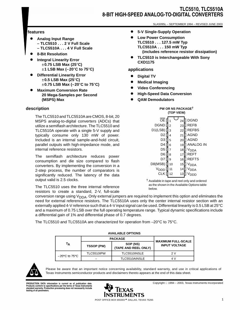
TLC5510, TLC5510A8-BIT HIGH-SPEED ANALOG-TO-DIGITAL CONVERTERS
SLAS095L – SEPTEMBER 1994 – REVISED JUNE 2003
1POST OFFICE BOX 655303 • DALLAS, TEXAS 75265
features
Analog Input Range– TLC5510 . . . 2 V Full Scale– TLC5510A . . . 4 V Full Scale
8-Bit Resolution
Integral Linearity Error±0.75 LSB Max (25°C)±1 LSB Max (–20°C to 75°C)
Differential Linearity Error±0.5 LSB Max (25°C)±0.75 LSB Max (–20°C to 75°C)
Maximum Conversion Rate20 Mega-Samples per Second(MSPS) Max
5-V Single-Supply Operation
Low Power ConsumptionTLC5510 . . . 127.5 mW TypTLC5510A . . . 150 mW Typ
(includes reference resistor dissipation)
TLC5510 is Interchangeable With SonyCXD1175
applications
Digital TV
Medical Imaging
Video Conferencing
High-Speed Data Conversion
QAM Demodulators
description
The TLC5510 and TLC5510A are CMOS, 8-bit, 20MSPS analog-to-digital converters (ADCs) thatutilize a semiflash architecture. The TLC5510 andTLC5510A operate with a single 5-V supply andtypically consume only 130 mW of power.Included is an internal sample-and-hold circuit,parallel outputs with high-impedance mode, andinternal reference resistors.
The semiflash architecture reduces powerconsumption and die size compared to flashconverters. By implementing the conversion in a2-step process, the number of comparators issignificantly reduced. The latency of the dataoutput valid is 2.5 clocks.
The TLC5510 uses the three internal referenceresistors to create a standard, 2-V, full-scaleconversion range using VDDA. Only external jumpers are required to implement this option and eliminates theneed for external reference resistors. The TLC5510A uses only the center internal resistor section with anexternally applied 4-V reference such that a 4-V input signal can be used. Differential linearity is 0.5 LSB at 25°Cand a maximum of 0.75 LSB over the full operating temperature range. Typical dynamic specifications includea differential gain of 1% and differential phase of 0.7 degrees.
The TLC5510 and TLC5510A are characterized for operation from –20°C to 75°C.
AVAILABLE OPTIONS
PACKAGEMAXIMUM FULL SCALE
TA TSSOP (PW)SOP (NS)
(TAPE AND REEL ONLY)
MAXIMUM FULL-SCALEINPUT VOLTAGE
20°C to 75°CTLC5510IPW TLC5510INSLE 2 V
–20°C to 75°C– TLC5510AINSLE 4 V
Please be aware that an important notice concerning availability, standard warranty, and use in critical applications ofTexas Instruments semiconductor products and disclaimers thereto appears at the end of this data sheet.
Copyright 1994 – 2003, Texas Instruments IncorporatedPRODUCTION DATA information is current as of publication date.Products conform to specifications per the terms of Texas Instrumentsstandard warranty. Production processing does not necessarily includetesting of all parameters.
1
2
3
4
5
6
7
8
9
10
11
12
24
23
22
21
20
19
18
17
16
15
14
13
OEDGND
D1(LSB)D2D3D4D5D6D7
D8(MSB)VDDD
CLK
DGNDREFBREFBSAGNDAGNDANALOG INVDDAREFTREFTSVDDAVDDAVDDD
PW OR NS PACKAGE†
(TOP VIEW)
† Available in tape and reel only and orderedas the shown in the Available Options tablebelow.
TLC5510, TLC5510A8-BIT HIGH-SPEED ANALOG-TO-DIGITAL CONVERTERS
SLAS095L – SEPTEMBER 1994 – REVISED JUNE 2003
2 POST OFFICE BOX 655303 • DALLAS, TEXAS 75265
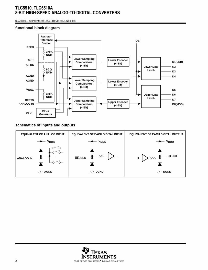
functional block diagram
Lower SamplingComparators
(4-Bit)
Lower Encoder(4-Bit)
Lower DataLatch
Lower SamplingComparators
(4-Bit)
Lower Encoder(4-Bit)
Upper SamplingComparators
(4-Bit)
Upper Encoder(4-Bit)
Upper DataLatch
ClockGenerator
OE
D1(LSB)
D2
D3
D4
D5
D6
D7
D8(MSB)
CLK
REFB
REFT
REFBS
AGND
AGND
ANALOG IN
VDDA
REFTS
270 ΩNOM
80 ΩNOM
320 ΩNOM
ResistorReference
Divider
schematics of inputs and outputs
EQUIVALENT OF ANALOG INPUT
VDDA
AGND
ANALOG IN
EQUIVALENT OF EACH DIGITAL INPUT
VDDD
DGND
OE, CLK
EQUIVALENT OF EACH DIGITAL OUTPUT
VDDD
DGND
D1–D8
TLC5510, TLC5510A8-BIT HIGH-SPEED ANALOG-TO-DIGITAL CONVERTERS
SLAS095L – SEPTEMBER 1994 – REVISED JUNE 2003
3POST OFFICE BOX 655303 • DALLAS, TEXAS 75265
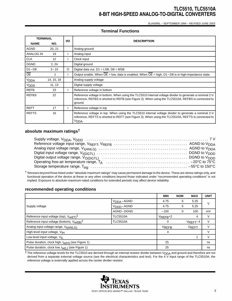
Terminal Functions
TERMINALI/O DESCRIPTION
NAME NO.I/O DESCRIPTION
AGND 20, 21 Analog ground
ANALOG IN 19 I Analog input
CLK 12 I Clock input
DGND 2, 24 Digital ground
D1–D8 3–10 O Digital data out. D1 = LSB, D8 = MSB
OE 1 I Output enable. When OE = low, data is enabled. When OE = high, D1–D8 is in high-impedance state.
VDDA 14, 15, 18 Analog supply voltage
VDDD 11, 13 Digital supply voltage
REFB 23 I Reference voltage in bottom
REFBS 22 Reference voltage in bottom. When using the TLC5510 internal voltage divider to generate a nominal 2-Vreference, REFBS is shorted to REFB (see Figure 3). When using the TLC5510A, REFBS is connected toground.
REFT 17 I Reference voltage in top
REFTS 16 Reference voltage in top. When using the TLC5510 internal voltage divider to generate a nominal 2-Vreference, REFTS is shorted to REFT (see Figure 3). When using the TLC5510A, REFTS is connected toVDDA.
absolute maximum ratings†
Supply voltage, VDDA, VDDD 7 V. . . . . . . . . . . . . . . . . . . . . . . . . . . . . . . . . . . . . . . . . . . . . . . . . . . . . . . . . . . . . . . . . Reference voltage input range, VREFT, VREFB AGND to VDDA. . . . . . . . . . . . . . . . . . . . . . . . . . . . . . . . . . . . . . . Analog input voltage range, VI(ANLG) AGND to VDDA. . . . . . . . . . . . . . . . . . . . . . . . . . . . . . . . . . . . . . . . . . . . . . . Digital input voltage range, VI(DGTL) DGND to VDDD. . . . . . . . . . . . . . . . . . . . . . . . . . . . . . . . . . . . . . . . . . . . . . . . Digital output voltage range, VO(DGTL) DGND to VDDD. . . . . . . . . . . . . . . . . . . . . . . . . . . . . . . . . . . . . . . . . . . . . Operating free-air temperature range, TA –20°C to 75°C. . . . . . . . . . . . . . . . . . . . . . . . . . . . . . . . . . . . . . . . . . . . Storage temperature range, Tstg –55°C to 150°C. . . . . . . . . . . . . . . . . . . . . . . . . . . . . . . . . . . . . . . . . . . . . . . . . . .
† Stresses beyond those listed under “absolute maximum ratings” may cause permanent damage to the device. These are stress ratings only, andfunctional operation of the device at these or any other conditions beyond those indicated under “recommended operating conditions” is notimplied. Exposure to absolute-maximum-rated conditions for extended periods may affect device reliability.
recommended operating conditions
MIN NOM MAX UNIT
VDDA–AGND 4.75 5 5.25V
Supply voltage VDDD–AGND 4.75 5 5.25V
AGND–DGND –100 0 100 mV
Reference input voltage (top), Vref(T)‡ TLC5510A VREFB+2 4 V
Reference input voltage (bottom), Vref(B)‡ TLC5510A 0 VREFT–4 V
Analog input voltage range, VI(ANLG) VREFB VREFT V
High-level input voltage, VIH 4 V
Low-level input voltage, VIL 1 V
Pulse duration, clock high, tw(H) (see Figure 1) 25 ns
Pulse duration, clock low, tw(L) (see Figure 1) 25 ns
‡ The reference voltage levels for the TLC5510 are derived through an internal resistor divider between VDDA and ground and therefore are notderived from a separate external voltage source (see the electrical characteristics and text). For the 4 V input range of the TLC5510A, thereference voltage is externally applied across the center divider resistor.
TLC5510, TLC5510A8-BIT HIGH-SPEED ANALOG-TO-DIGITAL CONVERTERS
SLAS095L – SEPTEMBER 1994 – REVISED JUNE 2003
4 POST OFFICE BOX 655303 • DALLAS, TEXAS 75265
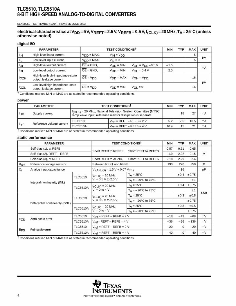
electrical characteristics at VDD = 5 V, VREFT = 2.5 V, VREFB = 0.5 V, f(CLK) = 20 MHz, TA = 25°C (unlessotherwise noted)
digital I/OPARAMETER TEST CONDITIONS† MIN TYP MAX UNIT
IIH High-level input current VDD = MAX, VIH = VDD 5µA
IIL Low-level input current VDD = MAX, VIL = 0 5µA
IOH High-level output current OE = GND, VDD = MIN, VOH = VDD–0.5 V –1.5mA
IOL Low-level output current OE = GND, VDD = MIN, VOL = 0.4 V 2.5mA
IOZHHigh-level high-impedance-stateoutput leakage current
OE = VDD, VDD = MAX VOH = VDD 16
µA
IOZLLow-level high-impedance-stateoutput leakage current
OE = VDD, VDD = MIN VOL = 0 16
µA
† Conditions marked MIN or MAX are as stated in recommended operating conditions.
powerPARAMETER TEST CONDITIONS† MIN TYP MAX UNIT
IDD Supply currentf(CLK) = 20 MHz, National Television System Committee (NTSC)ramp wave input, reference resistor dissipation is separate
18 27 mA
I f Reference voltage currentTLC5510 Vref = REFT – REFB = 2 V 5.2 7.5 10.5 mA
Iref Reference voltage currentTLC5510A Vref = REFT – REFB = 4 V 10.4 15 21 mA
† Conditions marked MIN or MAX are as stated in recommended operating conditions.
static performancePARAMETER TEST CONDITIONS† MIN TYP MAX UNIT
Self-bias (1), at REFBShort REFB to REFBS Short REFT to REFTS
0.57 0.61 0.65
Self-bias (2), REFT – REFBShort REFB to REFBS, Short REFT to REFTS
1.9 2.02 2.15 V
Self-bias (3), at REFT Short REFB to AGND, Short REFT to REFTS 2.18 2.29 2.4
Rref Reference voltage resistor Between REFT and REFB 190 270 350 Ω
Ci Analog input capacitance VI(ANLG) = 1.5 V + 0.07 Vrms 16 pF
TLC5510f(CLK) = 20 MHz, TA = 25°C ±0.4 ±0.75
Integral nonlinearity (INL)
TLC5510 (CLK) ,VI = 0.5 V to 2.5 V TA = –20°C to 75°C ±1
Integral nonlinearity (INL)
TLC5510Af(CLK) = 20 MHz, TA = 25°C ±0.4 ±0.75
TLC5510A (CLK) ,VI = 0 to 4 V TA = –20°C to 75°C ±1
LSB
TLC5510f(CLK) = 20 MHz, TA = 25°C ±0.3 ±0.5
LSB
Differential nonlinearity (DNL)
TLC5510 (CLK) ,VI = 0.5 V to 2.5 V TA = –20°C to 75°C ±0.75
Differential nonlinearity (DNL)
TLC5510Af(CLK) = 20 MHz, TA = 25°C ±0.3 ±0.5
TLC5510A (CLK) ,VI = 0 to 4 V TA = –20°C to 75°C ±0.75
EZS Zero scale errorTLC5510 Vref = REFT – REFB = 2 V –18 –43 –68 mV
EZS Zero-scale errorTLC5510A Vref= REFT – REFB = 4 V –36 –86 –136 mV
EFS Full-scale errorTLC5510 Vref = REFT – REFB = 2 V –20 0 20 mV
EFS Full-scale errorTLC5510A Vref = REFT – REFB = 4 V –40 0 40 mV
† Conditions marked MIN or MAX are as stated in recommended operating conditions.
TLC5510, TLC5510A8-BIT HIGH-SPEED ANALOG-TO-DIGITAL CONVERTERS
SLAS095L – SEPTEMBER 1994 – REVISED JUNE 2003
5POST OFFICE BOX 655303 • DALLAS, TEXAS 75265
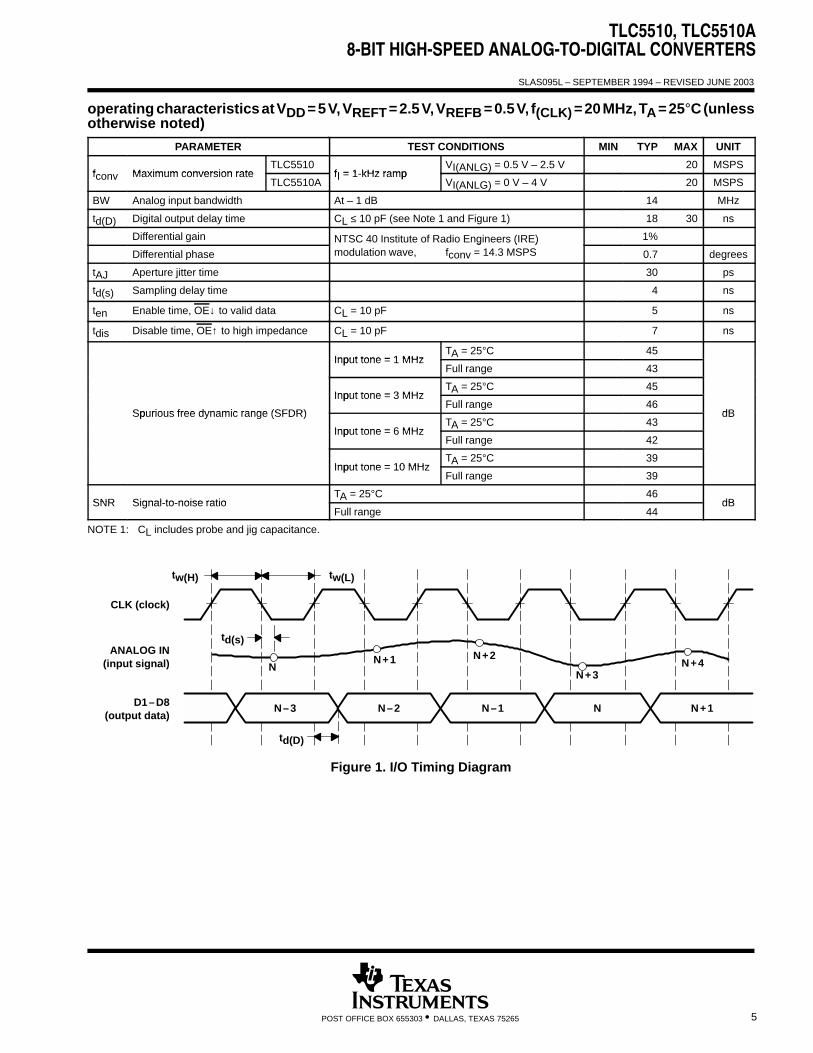
operating characteristics at VDD = 5 V, VREFT = 2.5 V, VREFB = 0.5 V, f(CLK) = 20 MHz, TA = 25°C (unlessotherwise noted)
PARAMETER TEST CONDITIONS MIN TYP MAX UNIT
f Maximum conversion rateTLC5510
fI = 1 kHz rampVI(ANLG) = 0.5 V – 2.5 V 20 MSPS
fconv Maximum conversion rateTLC5510A
fI = 1-kHz rampVI(ANLG) = 0 V – 4 V 20 MSPS
BW Analog input bandwidth At – 1 dB 14 MHz
td(D) Digital output delay time CL ≤ 10 pF (see Note 1 and Figure 1) 18 30 ns
Differential gain NTSC 40 Institute of Radio Engineers (IRE) 1%
Differential phase
g ( )modulation wave, fconv = 14.3 MSPS 0.7 degrees
tAJ Aperture jitter time 30 ps
td(s) Sampling delay time 4 ns
ten Enable time, OE↓ to valid data CL = 10 pF 5 ns
tdis Disable time, OE↑ to high impedance CL = 10 pF 7 ns
Input tone = 1 MHzTA = 25°C 45
Input tone = 1 MHzFull range 43
Input tone = 3 MHzTA = 25°C 45
Spurious free dynamic range (SFDR)
Input tone = 3 MHzFull range 46
dBSpurious free dynamic range (SFDR)
Input tone = 6 MHzTA = 25°C 43
dB
Input tone = 6 MHzFull range 42
Input tone = 10 MHzTA = 25°C 39
Input tone = 10 MHzFull range 39
SNR Signal to noise ratioTA = 25°C 46
dBSNR Signal-to-noise ratioFull range 44
dB
NOTE 1: CL includes probe and jig capacitance.
NN+1 N+2
N+3N+4
N–3 N–2 N–1 N N+1
td(D)
CLK (clock)
ANALOG IN(input signal)
D1–D8(output data)
tw(H) tw(L)
td(s)
Figure 1. I/O Timing Diagram
TLC5510, TLC5510A8-BIT HIGH-SPEED ANALOG-TO-DIGITAL CONVERTERS
SLAS095L – SEPTEMBER 1994 – REVISED JUNE 2003
6 POST OFFICE BOX 655303 • DALLAS, TEXAS 75265
PRINCIPLES OF OPERATION
functional description
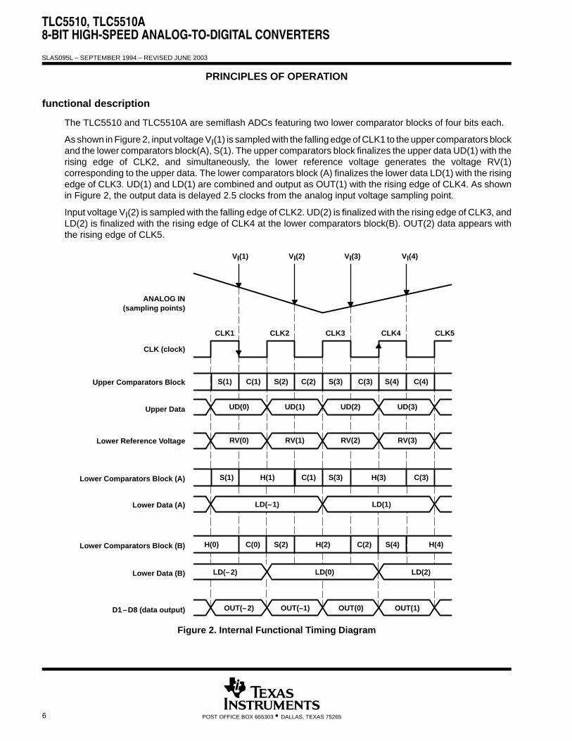
The TLC5510 and TLC5510A are semiflash ADCs featuring two lower comparator blocks of four bits each.
As shown in Figure 2, input voltage VI(1) is sampled with the falling edge of CLK1 to the upper comparators blockand the lower comparators block(A), S(1). The upper comparators block finalizes the upper data UD(1) with therising edge of CLK2, and simultaneously, the lower reference voltage generates the voltage RV(1)corresponding to the upper data. The lower comparators block (A) finalizes the lower data LD(1) with the risingedge of CLK3. UD(1) and LD(1) are combined and output as OUT(1) with the rising edge of CLK4. As shownin Figure 2, the output data is delayed 2.5 clocks from the analog input voltage sampling point.
Input voltage VI(2) is sampled with the falling edge of CLK2. UD(2) is finalized with the rising edge of CLK3, andLD(2) is finalized with the rising edge of CLK4 at the lower comparators block(B). OUT(2) data appears withthe rising edge of CLK5.
VI(1) VI(2) VI(3) VI(4)
CLK1 CLK2 CLK3 CLK4
S(1) C(1) S(2) C(2) S(3) C(3) S(4) C(4)
S(1) H(1) C(1) S(3) H(3) C(3)
H(0) C(0) S(2) H(2) C(2) S(4) H(4)
LD(–2)
OUT(–2) OUT(–1) OUT(0) OUT(1)
ANALOG IN(sampling points)
CLK (clock)
Upper Comparators Block
Upper Data
Lower Reference Voltage
Lower Comparators Block (A)
Lower Data (A)
Lower Comparators Block (B)
Lower Data (B)
D1–D8 (data output)
UD(0)
RV(0)
UD(1)
RV(1)
UD(2)
RV(2)
UD(3)
RV(3)
LD(–1)
LD(0)
LD(1)
LD(2)
CLK5
Figure 2. Internal Functional Timing Diagram
TLC5510, TLC5510A8-BIT HIGH-SPEED ANALOG-TO-DIGITAL CONVERTERS
SLAS095L – SEPTEMBER 1994 – REVISED JUNE 2003
7POST OFFICE BOX 655303 • DALLAS, TEXAS 75265
PRINCIPLES OF OPERATION
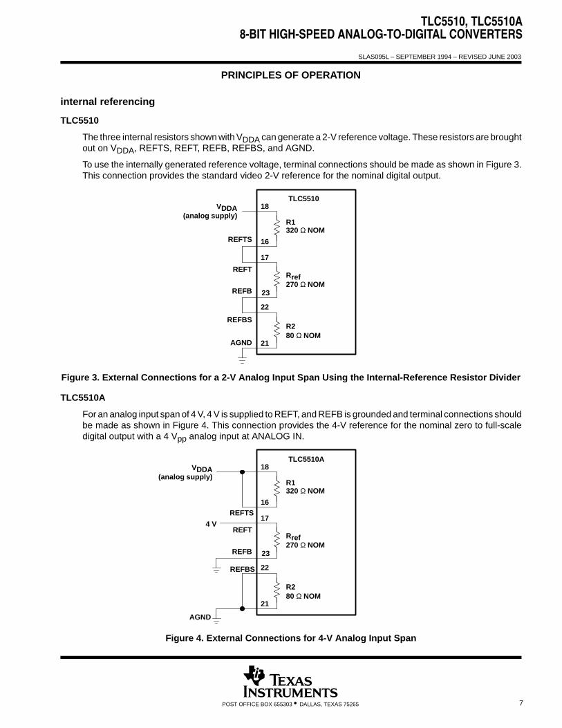
internal referencing
TLC5510
The three internal resistors shown with VDDA can generate a 2-V reference voltage. These resistors are broughtout on VDDA, REFTS, REFT, REFB, REFBS, and AGND.
To use the internally generated reference voltage, terminal connections should be made as shown in Figure 3.This connection provides the standard video 2-V reference for the nominal digital output.
R1320 Ω NOM
Rref270 Ω NOM
R280 Ω NOM
VDDA(analog supply)
REFTS
REFT
REFB
REFBS
AGND
TLC5510
16
17
22
21
23
18
Figure 3. External Connections for a 2-V Analog Input Span Using the Internal-Reference Resistor Divider
TLC5510A
For an analog input span of 4 V, 4 V is supplied to REFT, and REFB is grounded and terminal connections shouldbe made as shown in Figure 4. This connection provides the 4-V reference for the nominal zero to full-scaledigital output with a 4 Vpp analog input at ANALOG IN.
R1320 Ω NOM
Rref270 Ω NOM
R280 Ω NOM
REFTS
REFT
REFB
REFBS
AGND
TLC5510A
16
17
22
21
23
18
4 V
VDDA(analog supply)
Figure 4. External Connections for 4-V Analog Input Span
TLC5510, TLC5510A8-BIT HIGH-SPEED ANALOG-TO-DIGITAL CONVERTERS
SLAS095L – SEPTEMBER 1994 – REVISED JUNE 2003
8 POST OFFICE BOX 655303 • DALLAS, TEXAS 75265
PRINCIPLES OF OPERATION
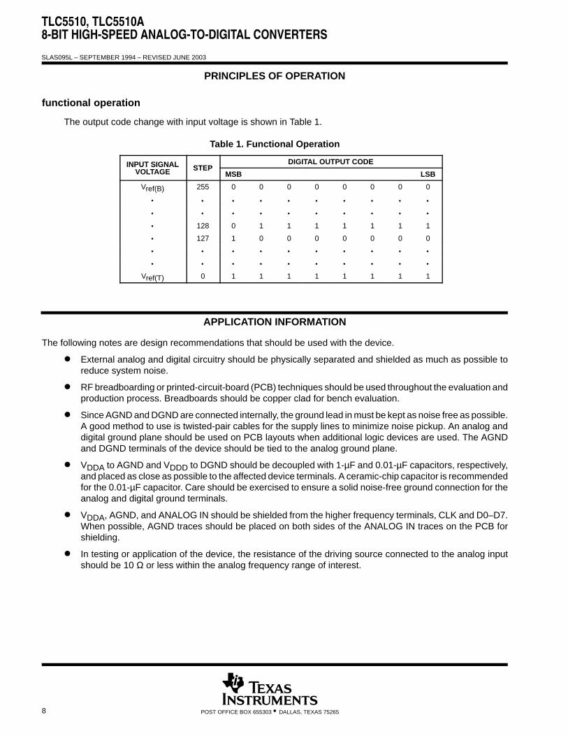
functional operation
The output code change with input voltage is shown in Table 1.
Table 1. Functional Operation
INPUT SIGNAL STEPDIGITAL OUTPUT CODEINPUT SIGNAL
VOLTAGE STEPMSB LSB
Vref(B) 255 0 0 0 0 0 0 0 0
• • • • • • • • • •
• • • • • • • • • •
• 128 0 1 1 1 1 1 1 1
• 127 1 0 0 0 0 0 0 0
• • • • • • • • • •
• • • • • • • • • •
Vref(T) 0 1 1 1 1 1 1 1 1
APPLICATION INFORMATION
The following notes are design recommendations that should be used with the device.
External analog and digital circuitry should be physically separated and shielded as much as possible toreduce system noise.
RF breadboarding or printed-circuit-board (PCB) techniques should be used throughout the evaluation andproduction process. Breadboards should be copper clad for bench evaluation.
Since AGND and DGND are connected internally, the ground lead in must be kept as noise free as possible.A good method to use is twisted-pair cables for the supply lines to minimize noise pickup. An analog anddigital ground plane should be used on PCB layouts when additional logic devices are used. The AGNDand DGND terminals of the device should be tied to the analog ground plane.
VDDA to AGND and VDDD to DGND should be decoupled with 1-µF and 0.01-µF capacitors, respectively,and placed as close as possible to the affected device terminals. A ceramic-chip capacitor is recommendedfor the 0.01-µF capacitor. Care should be exercised to ensure a solid noise-free ground connection for theanalog and digital ground terminals.
VDDA, AGND, and ANALOG IN should be shielded from the higher frequency terminals, CLK and D0–D7.When possible, AGND traces should be placed on both sides of the ANALOG IN traces on the PCB forshielding.
In testing or application of the device, the resistance of the driving source connected to the analog inputshould be 10 Ω or less within the analog frequency range of interest.
TLC5510, TLC5510A8-BIT HIGH-SPEED ANALOG-TO-DIGITAL CONVERTERS
SLAS095L – SEPTEMBER 1994 – REVISED JUNE 2003
9POST OFFICE BOX 655303 • DALLAS, TEXAS 75265
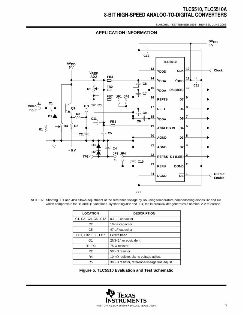
APPLICATION INFORMATION
C1
D1
C3
C4
C5
C6
C2
C11
C9
C7
C8
C10
C12
R5
R4 R2R1
Q1
D3
D2TP3
R3
C11FB2
FB3
FB7
FB1
VREFADJ
TP1J1
VDDD
VDDA
VDDA
REFTS
REFT
VDDA
ANALOG IN
AGND
AGND
REFBS
REFB
DGND
12
11
10
9
8
7
6
5
4
3
2
1
13
14
15
16
17
18
19
20
21
22
23
24
CLK
VDDD
D8 (MSB)
D7
D6
D5
D4
D3
D2
D1 (LSB)
DGND
OE
TLC5510AVDD5 V
Clock
OutputEnable
DVDD5 V
VideoInput
JP2JP1
JP4JP3– 5 V
NOTE A: Shorting JP1 and JP3 allows adjustment of the reference voltage by R5 using temperature-compensating diodes D2 and D3which compensate for D1 and Q1 variations. By shorting JP2 and JP4, the internal divider generates a nominal 2-V reference.
LOCATION DESCRIPTION
C1, C3–C4, C6–C12 0.1-µF capacitor
C2 10-pF capacitor
C5 47-µF capacitor
FB1, FB2, FB3, FB7 Ferrite bead
Q1 2N3414 or equivalent
R1, R3 75-Ω resistor
R2 500-Ω resistor
R4 10-kΩ resistor, clamp voltage adjust
R5 300-Ω resistor, reference-voltage fine adjust
Figure 5. TLC5510 Evaluation and Test Schematic
TLC5510, TLC5510A8-BIT HIGH-SPEED ANALOG-TO-DIGITAL CONVERTERS
SLAS095L – SEPTEMBER 1994 – REVISED JUNE 2003
10 POST OFFICE BOX 655303 • DALLAS, TEXAS 75265
APPLICATION INFORMATION
C1
D1
C3
C5
C6
C2
C11
C9
C7
C8
C4
R5
R4 R2R1
Q1
R3
C11FB2
FB3
FB7
FB1
VREFADJ
TP1J1
VDDD
VDDA
VDDA
REFTS
REFT
VDDA
ANALOG IN
AGND
AGND
REFBS
REFB
DGND
12
11
10
9
8
7
6
5
4
3
2
1
13
14
15
16
17
18
19
20
21
22
23
24
CLK
VDDD
D8 (MSB)
D7
D6
D5
D4
D3
D2
D1 (LSB)
DGND
OE
TLC5510AAVDD5 V
Clock
OutputEnable
DVDD5 V
VideoInput
– 5 V
NOTE A: R5 allows adjustment of the reference voltage to 4 V. R4 adjusts for the desired Q1 quiescent operating point.
LOCATION DESCRIPTION
C1, C3–C4, C6–C11 0.1-µF capacitor
C2 10-pF capacitor
C5 47-µF capacitor
FB1, FB2, FB3, FB7 Ferrite bead
Q1 2N3414 or equivalent
R1, R3 75-Ω resistor
R2 500-Ω resistor
R4 10-kΩ resistor, clamp voltage adjust
R5 300-Ω resistor, reference-voltage fine adjust
Figure 6. TLC5510A Evaluation and Test Schematic
TLC5510, TLC5510A8-BIT HIGH-SPEED ANALOG-TO-DIGITAL CONVERTERS
SLAS095L – SEPTEMBER 1994 – REVISED JUNE 2003
11POST OFFICE BOX 655303 • DALLAS, TEXAS 75265
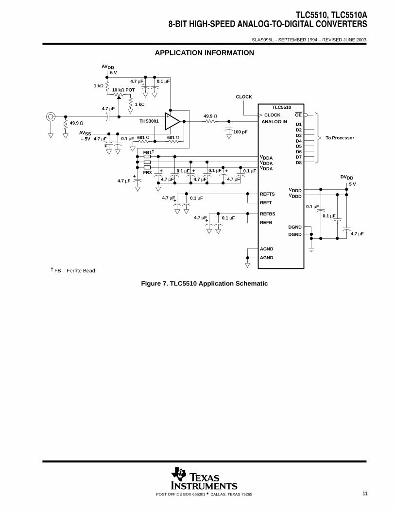
APPLICATION INFORMATION
CLOCK
CLOCK
ANALOG INOE
D1D2D3D4D5D6D7D8
To Processor100 pF
49.9 Ω
0.1 µF
4.7 µF
0.1 µF +
4.7 µF
+0.1 µF
4.7 µF
+
FB1†
FB3
_+
0.1 µF
+
4.7 µFAVSS
0.1 µF4.7 µF+
1 kΩ
AVDD
10 kΩ POT1 kΩ
4.7 µF
49.9 Ω
VDDAVDDAVDDA
REFTS
REFT
+4.7 µF
0.1 µF4.7 µF+
REFBS
REFB0.1 µF4.7 µF
+
AGND
AGND
681 Ω
VDDDVDDD
DGND
DGND
0.1 µF
0.1 µF
4.7 µF
DVDD
TLC5510
THS3001
681 Ω
5 V
– 5V
† FB – Ferrite Bead
5 V
Figure 7. TLC5510 Application Schematic
TLC5510, TLC5510A8-BIT HIGH-SPEED ANALOG-TO-DIGITAL CONVERTERS
SLAS095L – SEPTEMBER 1994 – REVISED JUNE 2003
12 POST OFFICE BOX 655303 • DALLAS, TEXAS 75265
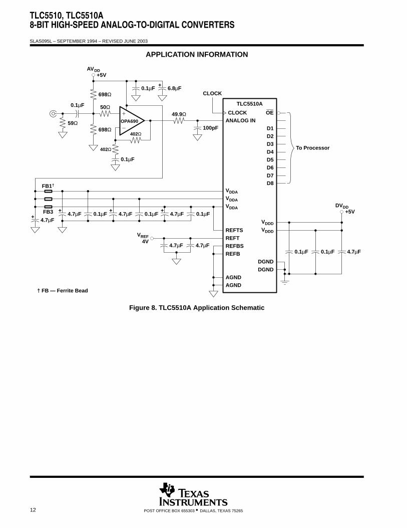
APPLICATION INFORMATION
50Ω
AVDD
0.1µF
402Ω
49.9ΩOPA69059Ω
698Ω
698Ω
+6.8µF0.1µF
100pF
4.7µF 0.1µF 4.7µF 0.1µF 4.7µF
0.1µF 0.1µF 4.7µF4.7µF 4.7µF
0.1µF4.7µF
0.1µF
+5V
DVDD+5V
TLC5510A
CLOCK
CLOCK
ANALOG IN
VDDA
VDDA
VDDA
REFTSREFTREFBSREFB
AGNDAGND
OE
D1D2D3D4
To Processor
D5D6
D7D8
VDDD
VDDD
DGND
DGND
FB1†
FB3
VREF4V
++ + +
† FB — Ferrite Bead
402Ω
Figure 8. TLC5510A Application Schematic
PACKAGE OPTION ADDENDUM
www.ti.com 17-Mar-2017
Addendum-Page 1
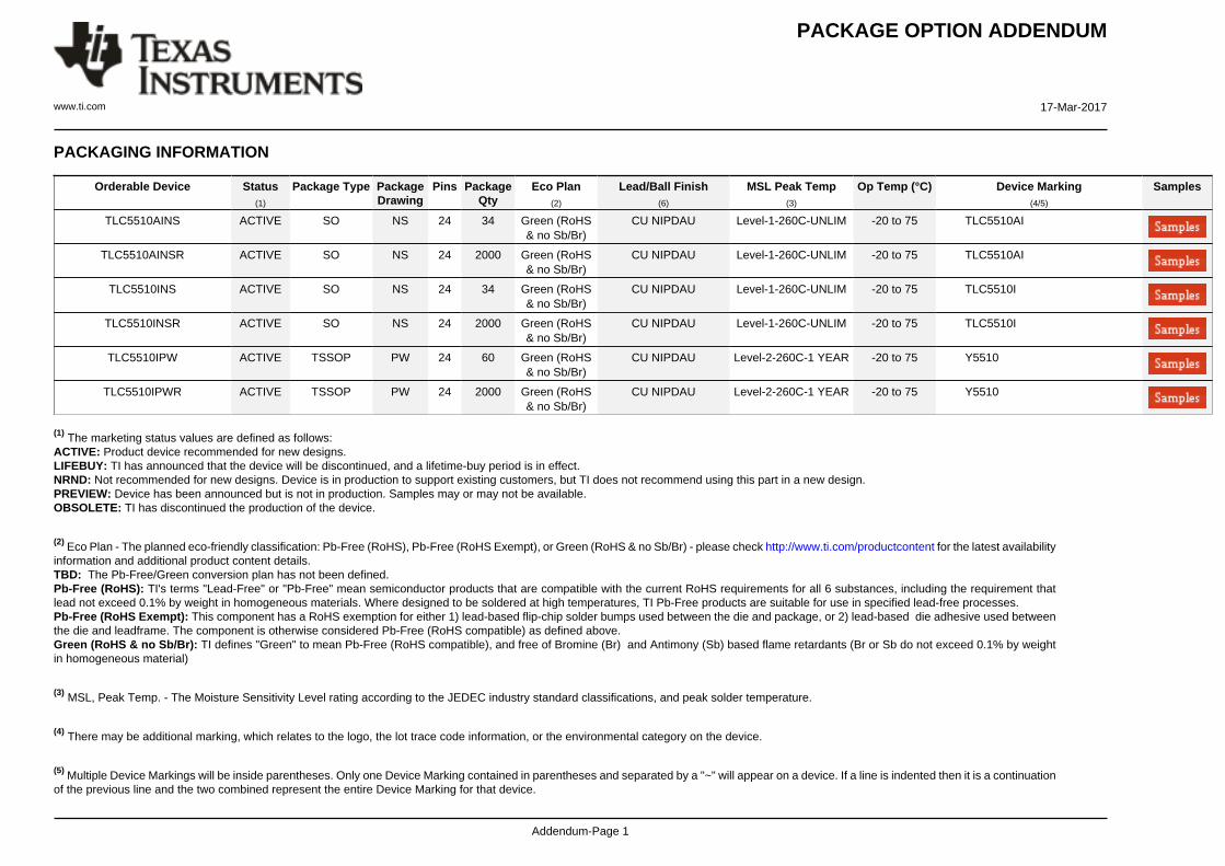
PACKAGING INFORMATION
Orderable Device Status(1)
Package Type PackageDrawing
Pins PackageQty
Eco Plan(2)
Lead/Ball Finish(6)
MSL Peak Temp(3)
Op Temp (°C) Device Marking(4/5)
Samples
TLC5510AINS ACTIVE SO NS 24 34 Green (RoHS& no Sb/Br)
CU NIPDAU Level-1-260C-UNLIM -20 to 75 TLC5510AI
TLC5510AINSR ACTIVE SO NS 24 2000 Green (RoHS& no Sb/Br)
CU NIPDAU Level-1-260C-UNLIM -20 to 75 TLC5510AI
TLC5510INS ACTIVE SO NS 24 34 Green (RoHS& no Sb/Br)
CU NIPDAU Level-1-260C-UNLIM -20 to 75 TLC5510I
TLC5510INSR ACTIVE SO NS 24 2000 Green (RoHS& no Sb/Br)
CU NIPDAU Level-1-260C-UNLIM -20 to 75 TLC5510I
TLC5510IPW ACTIVE TSSOP PW 24 60 Green (RoHS& no Sb/Br)
CU NIPDAU Level-2-260C-1 YEAR -20 to 75 Y5510
TLC5510IPWR ACTIVE TSSOP PW 24 2000 Green (RoHS& no Sb/Br)
CU NIPDAU Level-2-260C-1 YEAR -20 to 75 Y5510
(1) The marketing status values are defined as follows:ACTIVE: Product device recommended for new designs.LIFEBUY: TI has announced that the device will be discontinued, and a lifetime-buy period is in effect.NRND: Not recommended for new designs. Device is in production to support existing customers, but TI does not recommend using this part in a new design.PREVIEW: Device has been announced but is not in production. Samples may or may not be available.OBSOLETE: TI has discontinued the production of the device.
(2) Eco Plan - The planned eco-friendly classification: Pb-Free (RoHS), Pb-Free (RoHS Exempt), or Green (RoHS & no Sb/Br) - please check http://www.ti.com/productcontent for the latest availabilityinformation and additional product content details.TBD: The Pb-Free/Green conversion plan has not been defined.Pb-Free (RoHS): TI's terms "Lead-Free" or "Pb-Free" mean semiconductor products that are compatible with the current RoHS requirements for all 6 substances, including the requirement thatlead not exceed 0.1% by weight in homogeneous materials. Where designed to be soldered at high temperatures, TI Pb-Free products are suitable for use in specified lead-free processes.Pb-Free (RoHS Exempt): This component has a RoHS exemption for either 1) lead-based flip-chip solder bumps used between the die and package, or 2) lead-based die adhesive used betweenthe die and leadframe. The component is otherwise considered Pb-Free (RoHS compatible) as defined above.Green (RoHS & no Sb/Br): TI defines "Green" to mean Pb-Free (RoHS compatible), and free of Bromine (Br) and Antimony (Sb) based flame retardants (Br or Sb do not exceed 0.1% by weightin homogeneous material)
(3) MSL, Peak Temp. - The Moisture Sensitivity Level rating according to the JEDEC industry standard classifications, and peak solder temperature.
(4) There may be additional marking, which relates to the logo, the lot trace code information, or the environmental category on the device.
(5) Multiple Device Markings will be inside parentheses. Only one Device Marking contained in parentheses and separated by a "~" will appear on a device. If a line is indented then it is a continuationof the previous line and the two combined represent the entire Device Marking for that device.
PACKAGE OPTION ADDENDUM
www.ti.com 17-Mar-2017
Addendum-Page 2
(6) Lead/Ball Finish - Orderable Devices may have multiple material finish options. Finish options are separated by a vertical ruled line. Lead/Ball Finish values may wrap to two lines if the finishvalue exceeds the maximum column width.
Important Information and Disclaimer:The information provided on this page represents TI's knowledge and belief as of the date that it is provided. TI bases its knowledge and belief on informationprovided by third parties, and makes no representation or warranty as to the accuracy of such information. Efforts are underway to better integrate information from third parties. TI has taken andcontinues to take reasonable steps to provide representative and accurate information but may not have conducted destructive testing or chemical analysis on incoming materials and chemicals.TI and TI suppliers consider certain information to be proprietary, and thus CAS numbers and other limited information may not be available for release.
In no event shall TI's liability arising out of such information exceed the total purchase price of the TI part(s) at issue in this document sold by TI to Customer on an annual basis.
TAPE AND REEL INFORMATION
*All dimensions are nominal
Device PackageType
PackageDrawing
Pins SPQ ReelDiameter
(mm)
ReelWidth
W1 (mm)
A0(mm)
B0(mm)
K0(mm)
P1(mm)
W(mm)
Pin1Quadrant
TLC5510AINSR SO NS 24 2000 330.0 24.4 8.5 15.3 2.6 12.0 24.0 Q1
TLC5510INSR SO NS 24 2000 330.0 24.4 8.5 15.3 2.6 12.0 24.0 Q1
TLC5510IPWR TSSOP PW 24 2000 330.0 16.4 6.95 8.3 1.6 8.0 16.0 Q1
PACKAGE MATERIALS INFORMATION
www.ti.com 13-May-2015
Pack Materials-Page 1
*All dimensions are nominal
Device Package Type Package Drawing Pins SPQ Length (mm) Width (mm) Height (mm)
TLC5510AINSR SO NS 24 2000 367.0 367.0 45.0
TLC5510INSR SO NS 24 2000 367.0 367.0 45.0
TLC5510IPWR TSSOP PW 24 2000 367.0 367.0 38.0
PACKAGE MATERIALS INFORMATION
www.ti.com 13-May-2015
Pack Materials-Page 2
IMPORTANT NOTICE
Texas Instruments Incorporated (TI) reserves the right to make corrections, enhancements, improvements and other changes to itssemiconductor products and services per JESD46, latest issue, and to discontinue any product or service per JESD48, latest issue. Buyersshould obtain the latest relevant information before placing orders and should verify that such information is current and complete.TI’s published terms of sale for semiconductor products (http://www.ti.com/sc/docs/stdterms.htm) apply to the sale of packaged integratedcircuit products that TI has qualified and released to market. Additional terms may apply to the use or sale of other types of TI products andservices.Reproduction of significant portions of TI information in TI data sheets is permissible only if reproduction is without alteration and isaccompanied by all associated warranties, conditions, limitations, and notices. TI is not responsible or liable for such reproduceddocumentation. Information of third parties may be subject to additional restrictions. Resale of TI products or services with statementsdifferent from or beyond the parameters stated by TI for that product or service voids all express and any implied warranties for theassociated TI product or service and is an unfair and deceptive business practice. TI is not responsible or liable for any such statements.Buyers and others who are developing systems that incorporate TI products (collectively, “Designers”) understand and agree that Designersremain responsible for using their independent analysis, evaluation and judgment in designing their applications and that Designers havefull and exclusive responsibility to assure the safety of Designers' applications and compliance of their applications (and of all TI productsused in or for Designers’ applications) with all applicable regulations, laws and other applicable requirements. Designer represents that, withrespect to their applications, Designer has all the necessary expertise to create and implement safeguards that (1) anticipate dangerousconsequences of failures, (2) monitor failures and their consequences, and (3) lessen the likelihood of failures that might cause harm andtake appropriate actions. Designer agrees that prior to using or distributing any applications that include TI products, Designer willthoroughly test such applications and the functionality of such TI products as used in such applications.TI’s provision of technical, application or other design advice, quality characterization, reliability data or other services or information,including, but not limited to, reference designs and materials relating to evaluation modules, (collectively, “TI Resources”) are intended toassist designers who are developing applications that incorporate TI products; by downloading, accessing or using TI Resources in anyway, Designer (individually or, if Designer is acting on behalf of a company, Designer’s company) agrees to use any particular TI Resourcesolely for this purpose and subject to the terms of this Notice.TI’s provision of TI Resources does not expand or otherwise alter TI’s applicable published warranties or warranty disclaimers for TIproducts, and no additional obligations or liabilities arise from TI providing such TI Resources. TI reserves the right to make corrections,enhancements, improvements and other changes to its TI Resources. TI has not conducted any testing other than that specificallydescribed in the published documentation for a particular TI Resource.Designer is authorized to use, copy and modify any individual TI Resource only in connection with the development of applications thatinclude the TI product(s) identified in such TI Resource. NO OTHER LICENSE, EXPRESS OR IMPLIED, BY ESTOPPEL OR OTHERWISETO ANY OTHER TI INTELLECTUAL PROPERTY RIGHT, AND NO LICENSE TO ANY TECHNOLOGY OR INTELLECTUAL PROPERTYRIGHT OF TI OR ANY THIRD PARTY IS GRANTED HEREIN, including but not limited to any patent right, copyright, mask work right, orother intellectual property right relating to any combination, machine, or process in which TI products or services are used. Informationregarding or referencing third-party products or services does not constitute a license to use such products or services, or a warranty orendorsement thereof. Use of TI Resources may require a license from a third party under the patents or other intellectual property of thethird party, or a license from TI under the patents or other intellectual property of TI.TI RESOURCES ARE PROVIDED “AS IS” AND WITH ALL FAULTS. TI DISCLAIMS ALL OTHER WARRANTIES ORREPRESENTATIONS, EXPRESS OR IMPLIED, REGARDING RESOURCES OR USE THEREOF, INCLUDING BUT NOT LIMITED TOACCURACY OR COMPLETENESS, TITLE, ANY EPIDEMIC FAILURE WARRANTY AND ANY IMPLIED WARRANTIES OFMERCHANTABILITY, FITNESS FOR A PARTICULAR PURPOSE, AND NON-INFRINGEMENT OF ANY THIRD PARTY INTELLECTUALPROPERTY RIGHTS. TI SHALL NOT BE LIABLE FOR AND SHALL NOT DEFEND OR INDEMNIFY DESIGNER AGAINST ANY CLAIM,INCLUDING BUT NOT LIMITED TO ANY INFRINGEMENT CLAIM THAT RELATES TO OR IS BASED ON ANY COMBINATION OFPRODUCTS EVEN IF DESCRIBED IN TI RESOURCES OR OTHERWISE. IN NO EVENT SHALL TI BE LIABLE FOR ANY ACTUAL,DIRECT, SPECIAL, COLLATERAL, INDIRECT, PUNITIVE, INCIDENTAL, CONSEQUENTIAL OR EXEMPLARY DAMAGES INCONNECTION WITH OR ARISING OUT OF TI RESOURCES OR USE THEREOF, AND REGARDLESS OF WHETHER TI HAS BEENADVISED OF THE POSSIBILITY OF SUCH DAMAGES.Unless TI has explicitly designated an individual product as meeting the requirements of a particular industry standard (e.g., ISO/TS 16949and ISO 26262), TI is not responsible for any failure to meet such industry standard requirements.Where TI specifically promotes products as facilitating functional safety or as compliant with industry functional safety standards, suchproducts are intended to help enable customers to design and create their own applications that meet applicable functional safety standardsand requirements. Using products in an application does not by itself establish any safety features in the application. Designers mustensure compliance with safety-related requirements and standards applicable to their applications. Designer may not use any TI products inlife-critical medical equipment unless authorized officers of the parties have executed a special contract specifically governing such use.Life-critical medical equipment is medical equipment where failure of such equipment would cause serious bodily injury or death (e.g., lifesupport, pacemakers, defibrillators, heart pumps, neurostimulators, and implantables). Such equipment includes, without limitation, allmedical devices identified by the U.S. Food and Drug Administration as Class III devices and equivalent classifications outside the U.S.TI may expressly designate certain products as completing a particular qualification (e.g., Q100, Military Grade, or Enhanced Product).Designers agree that it has the necessary expertise to select the product with the appropriate qualification designation for their applicationsand that proper product selection is at Designers’ own risk. Designers are solely responsible for compliance with all legal and regulatoryrequirements in connection with such selection.Designer will fully indemnify TI and its representatives against any damages, costs, losses, and/or liabilities arising out of Designer’s non-compliance with the terms and provisions of this Notice.
Mailing Address: Texas Instruments, Post Office Box 655303, Dallas, Texas 75265Copyright © 2017, Texas Instruments Incorporated