Embed Size (px)
Citation preview
FLIP-CHIP INTEGRATED SOI-CMOS-MEMS FABRICATION TECHNOLOGY P. J. Gilgunn1, G. K. Fedder1,2,3
1Electrical and Computer Engineering Dept., 2The Institute for Complex Engineered Systems, and 3The Robotics Institute, Carnegie Mellon University, Pittsburgh, Pennsylvania, USA
ABSTRACT
A fully-dry, flip-chip fabrication technology was developed for the integration of high fill factor, silicon-on-insulator (SOI) structures and CMOS-MEMS actuators. An SOI mirror array with a fill factor of 95% and radius of curvature >1.3 m was fabricated on CMOS-MEMS electrothermal actuators using this technology. The unloaded actuators achieved an optical scan range of >92º. Following flip-chip bonding with high temperature epoxy, the structures were released using deep reactive ion etching (DRIE). Aspect ratio dependent etching (ARDE) modulated local structural silicon thickness on the CMOS-MEMS actuators and reduced notching and microtrenching on the posts of the SOI mirrors.
INTRODUCTION
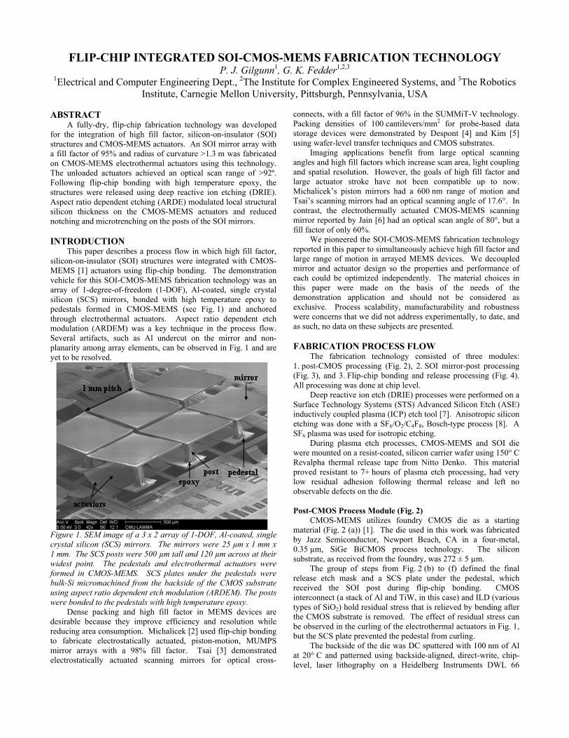
This paper describes a process flow in which high fill factor, silicon-on-insulator (SOI) structures were integrated with CMOS-MEMS [1] actuators using flip-chip bonding. The demonstration vehicle for this SOI-CMOS-MEMS fabrication technology was an array of 1-degree-of-freedom (1-DOF), Al-coated, single crystal silicon (SCS) mirrors, bonded with high temperature epoxy to pedestals formed in CMOS-MEMS (see Fig. 1) and anchored through electrothermal actuators. Aspect ratio dependent etch modulation (ARDEM) was a key technique in the process flow. Several artifacts, such as Al undercut on the mirror and non-planarity among array elements, can be observed in Fig. 1 and are yet to be resolved.
Figure 1. SEM image of a 3 x 2 array of 1-DOF, Al-coated, single crystal silicon (SCS) mirrors. The mirrors were 25 µm x 1 mm x 1 mm. The SCS posts were 500 µm tall and 120 µm across at their widest point. The pedestals and electrothermal actuators were formed in CMOS-MEMS. SCS plates under the pedestals were bulk-Si micromachined from the backside of the CMOS substrate using aspect ratio dependent etch modulation (ARDEM). The posts were bonded to the pedestals with high temperature epoxy.
Dense packing and high fill factor in MEMS devices are desirable because they improve efficiency and resolution while reducing area consumption. Michalicek [2] used flip-chip bonding to fabricate electrostatically actuated, piston-motion, MUMPS mirror arrays with a 98% fill factor. Tsai [3] demonstrated electrostatically actuated scanning mirrors for optical cross-
connects, with a fill factor of 96% in the SUMMiT-V technology. Packing densities of 100 cantilevers/mm2 for probe-based data storage devices were demonstrated by Despont [4] and Kim [5] using wafer-level transfer techniques and CMOS substrates.
Imaging applications benefit from large optical scanning angles and high fill factors which increase scan area, light coupling and spatial resolution. However, the goals of high fill factor and large actuator stroke have not been compatible up to now. Michalicek’s piston mirrors had a 600 nm range of motion and Tsai’s scanning mirrors had an optical scanning angle of 17.6°. In contrast, the electrothermally actuated CMOS-MEMS scanning mirror reported by Jain [6] had an optical scan angle of 80°, but a fill factor of only 60%.
We pioneered the SOI-CMOS-MEMS fabrication technology reported in this paper to simultaneously achieve high fill factor and large range of motion in arrayed MEMS devices. We decoupled mirror and actuator design so the properties and performance of each could be optimized independently. The material choices in this paper were made on the basis of the needs of the demonstration application and should not be considered as exclusive. Process scalability, manufacturability and robustness were concerns that we did not address experimentally, to date, and as such, no data on these subjects are presented. FABRICATION PROCESS FLOW
The fabrication technology consisted of three modules: 1. post-CMOS processing (Fig. 2), 2. SOI mirror-post processing (Fig. 3), and 3. Flip-chip bonding and release processing (Fig. 4). All processing was done at chip level.
Deep reactive ion etch (DRIE) processes were performed on a Surface Technology Systems (STS) Advanced Silicon Etch (ASE) inductively coupled plasma (ICP) etch tool [7]. Anisotropic silicon etching was done with a SF6/O2/C4F8, Bosch-type process [8]. A SF6 plasma was used for isotropic etching.
During plasma etch processes, CMOS-MEMS and SOI die were mounted on a resist-coated, silicon carrier wafer using 150° C Revalpha thermal release tape from Nitto Denko. This material proved resistant to 7+ hours of plasma etch processing, had very low residual adhesion following thermal release and left no observable defects on the die.
Post-CMOS Process Module (Fig. 2)
CMOS-MEMS utilizes foundry CMOS die as a starting material (Fig. 2 (a)) [1]. The die used in this work was fabricated by Jazz Semiconductor, Newport Beach, CA in a four-metal, 0.35 µm, SiGe BiCMOS process technology. The silicon substrate, as received from the foundry, was 272 ± 5 µm.
The group of steps from Fig. 2 (b) to (f) defined the final release etch mask and a SCS plate under the pedestal, which received the SOI post during flip-chip bonding. CMOS interconnect (a stack of Al and TiW, in this case) and ILD (various types of SiO2) hold residual stress that is relieved by bending after the CMOS substrate is removed. The effect of residual stress can be observed in the curling of the electrothermal actuators in Fig. 1, but the SCS plate prevented the pedestal from curling.
The backside of the die was DC sputtered with 100 nm of Al at 20° C and patterned using backside-aligned, direct-write, chip-level, laser lithography on a Heidelberg Instruments DWL 66
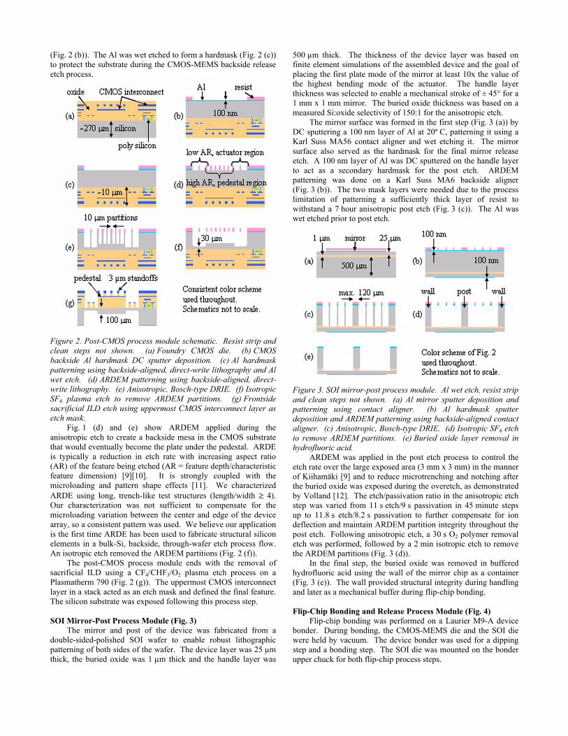
(Fig. 2 (b)). The Al was wet etched to form a hardmask (Fig. 2 (c)) to protect the substrate during the CMOS-MEMS backside release etch process.
Figure 2. Post-CMOS process module schematic. Resist strip and clean steps not shown. (a) Foundry CMOS die. (b) CMOS backside Al hardmask DC sputter deposition. (c) Al hardmask patterning using backside-aligned, direct-write lithography and Al wet etch. (d) ARDEM patterning using backside-aligned, direct-write lithography. (e) Anisotropic, Bosch-type DRIE. (f) Isotropic SF6 plasma etch to remove ARDEM partitions. (g) Frontside sacrificial ILD etch using uppermost CMOS interconnect layer as etch mask.
Fig. 1 (d) and (e) show ARDEM applied during the anisotropic etch to create a backside mesa in the CMOS substrate that would eventually become the plate under the pedestal. ARDE is typically a reduction in etch rate with increasing aspect ratio (AR) of the feature being etched (AR = feature depth/characteristic feature dimension) [9][10]. It is strongly coupled with the microloading and pattern shape effects [11]. We characterized ARDE using long, trench-like test structures (length/width ≥ 4). Our characterization was not sufficient to compensate for the microloading variation between the center and edge of the device array, so a consistent pattern was used. We believe our application is the first time ARDE has been used to fabricate structural silicon elements in a bulk-Si, backside, through-wafer etch process flow. An isotropic etch removed the ARDEM partitions (Fig. 2 (f)).
The post-CMOS process module ends with the removal of sacrificial ILD using a CF4/CHF3/O2 plasma etch process on a Plasmatherm 790 (Fig. 2 (g)). The uppermost CMOS interconnect layer in a stack acted as an etch mask and defined the final feature. The silicon substrate was exposed following this process step.
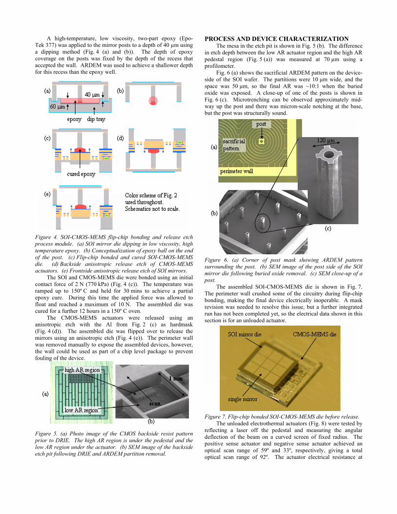
SOI Mirror-Post Process Module (Fig. 3)
The mirror and post of the device was fabricated from a double-sided-polished SOI wafer to enable robust lithographic patterning of both sides of the wafer. The device layer was 25 µm thick, the buried oxide was 1 µm thick and the handle layer was
500 µm thick. The thickness of the device layer was based on finite element simulations of the assembled device and the goal of placing the first plate mode of the mirror at least 10x the value of the highest bending mode of the actuator. The handle layer thickness was selected to enable a mechanical stroke of ± 45° for a 1 mm x 1 mm mirror. The buried oxide thickness was based on a measured Si:oxide selectivity of 150:1 for the anisotropic etch.
The mirror surface was formed in the first step (Fig. 3 (a)) by DC sputtering a 100 nm layer of Al at 20º C, patterning it using a Karl Suss MA56 contact aligner and wet etching it. The mirror surface also served as the hardmask for the final mirror release etch. A 100 nm layer of Al was DC sputtered on the handle layer to act as a secondary hardmask for the post etch. ARDEM patterning was done on a Karl Suss MA6 backside aligner (Fig. 3 (b)). The two mask layers were needed due to the process limitation of patterning a sufficiently thick layer of resist to withstand a 7 hour anisotropic post etch (Fig. 3 (c)). The Al was wet etched prior to post etch.
Figure 3. SOI mirror-post process module. Al wet etch, resist strip and clean steps not shown. (a) Al mirror sputter deposition and patterning using contact aligner. (b) Al hardmask sputter deposition and ARDEM patterning using backside-aligned contact aligner. (c) Anisotropic, Bosch-type DRIE. (d) Isotropic SF6 etch to remove ARDEM partitions. (e) Buried oxide layer removal in hydrofluoric acid.
ARDEM was applied in the post etch process to control the etch rate over the large exposed area (3 mm x 3 mm) in the manner of Kiihamäki [9] and to reduce microtrenching and notching after the buried oxide was exposed during the overetch, as demonstrated by Volland [12]. The etch/passivation ratio in the anisotropic etch step was varied from 11 s etch/9 s passivation in 45 minute steps up to 11.8 s etch/8.2 s passivation to further compensate for ion deflection and maintain ARDEM partition integrity throughout the post etch. Following anisotropic etch, a 30 s O2 polymer removal etch was performed, followed by a 2 min isotropic etch to remove the ARDEM partitions (Fig. 3 (d)).
In the final step, the buried oxide was removed in buffered hydrofluoric acid using the wall of the mirror chip as a container (Fig. 3 (e)). The wall provided structural integrity during handling and later as a mechanical buffer during flip-chip bonding.
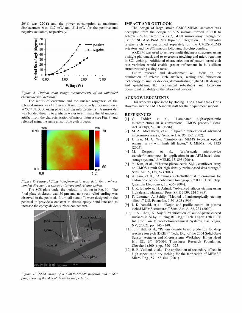
Flip-Chip Bonding and Release Process Module (Fig. 4)
Flip-chip bonding was performed on a Laurier M9-A device bonder. During bonding, the CMOS-MEMS die and the SOI die were held by vacuum. The device bonder was used for a dipping step and a bonding step. The SOI die was mounted on the bonder upper chuck for both flip-chip process steps.
A high-temperature, low viscosity, two-part epoxy (Epo-Tek 377) was applied to the mirror posts to a depth of 40 µm using a dipping method (Fig. 4 (a) and (b)). The depth of epoxy coverage on the posts was fixed by the depth of the recess that accepted the wall. ARDEM was used to achieve a shallower depth for this recess than the epoxy well.
Figure 4. SOI-CMOS-MEMS flip-chip bonding and release etch process module. (a) SOI mirror die dipping in low viscosity, high temperature epoxy. (b) Conceptualization of epoxy ball on the end of the post. (c) Flip-chip bonded and cured SOI-CMOS-MEMS die. (d) Backside anisotropic release etch of CMOS-MEMS actuators. (e) Frontside anisotropic release etch of SOI mirrors.
The SOI and CMOS-MEMS die were bonded using an initial contact force of 2 N (770 kPa) (Fig. 4 (c)). The temperature was ramped up to 150º C and held for 30 mins to achieve a partial epoxy cure. During this time the applied force was allowed to float and reached a maximum of 10 N. The assembled die was cured for a further 12 hours in a 150º C oven.
The CMOS-MEMS actuators were released using an anisotropic etch with the Al from Fig. 2 (c) as hardmask (Fig. 4 (d)). The assembled die was flipped over to release the mirrors using an anisotropic etch (Fig. 4 (e)). The perimeter wall was removed manually to expose the assembled devices, however, the wall could be used as part of a chip level package to prevent fouling of the device.
Figure 5. (a) Photo image of the CMOS backside resist pattern prior to DRIE. The high AR region is under the pedestal and the low AR region under the actuator. (b) SEM image of the backside etch pit following DRIE and ARDEM partition removal.
PROCESS AND DEVICE CHARACTERIZATION The mesa in the etch pit is shown in Fig. 5 (b). The difference
in etch depth between the low AR actuator region and the high AR pedestal region (Fig. 5 (a)) was measured at 70 µm using a profilometer.
Fig. 6 (a) shows the sacrificial ARDEM pattern on the device-side of the SOI wafer. The partitions were 10 µm wide, and the space was 50 µm, so the final AR was ~10:1 when the buried oxide was exposed. A close-up of one of the posts is shown in Fig. 6 (c). Microtrenching can be observed approximately mid-way up the post and there was micron-scale notching at the base, but the post was structurally sound.
Figure 6. (a) Corner of post mask showing ARDEM pattern surrounding the post. (b) SEM image of the post side of the SOI mirror die following buried oxide removal. (c) SEM close-up of a post.
The assembled SOI-CMOS-MEMS die is shown in Fig. 7. The perimeter wall crushed some of the circuitry during flip-chip bonding, making the final device electrically inoperable. A mask revision was needed to resolve this issue, but a further integrated run has not been completed yet, so the electrical data shown in this section is for an unloaded actuator.
Figure 7. Flip-chip bonded SOI-CMOS-MEMS die before release.
The unloaded electrothermal actuators (Fig. 8) were tested by reflecting a laser off the pedestal and measuring the angular deflection of the beam on a curved screen of fixed radius. The positive sense actuator and negative sense actuator achieved an optical scan range of 59º and 33º, respectively, giving a total optical scan range of 92º. The actuator electrical resistance at
20º C was 220 Ω and the power consumption at maximum displacement was 13.7 mW and 21.1 mW for the positive and negative actuators, respectively.
Figure 8. Optical scan range measurements of an unloaded electrothermal actuator.
The radius of curvature and the surface roughness of the released mirror was >1.3 m and 8 nm, respectively, measured on a WYCO NT3300 using phase shifting interferometry. A mirror die was bonded directly to a silicon wafer to eliminate the Al undercut artifact from the characterization of mirror flatness (see Fig. 9) and released using the same anisotropic etch process.
Figure 9. Phase shifting interferometric scan data for a mirror bonded directly to a silicon substrate and release etched.
The SCS plate under the pedestal is shown in Fig. 10. The final plate thickness was 50 µm and no stress relief curling was observed in the pedestal. 3 µm tall standoffs were designed on the pedestal to provide a constant thickness epoxy bond line and to increase the epoxy-device surface contact area.
Figure 10. SEM image of a CMOS-MEMS pedestal and a SOI post, showing the SCS plate under the pedestal.
IMPACT AND OUTLOOK The design of large stroke CMOS-MEMS actuators was
decoupled from the design of SCS mirrors formed in SOI to achieve 95% fill factor in a 3 x 2, 1-DOF mirror array, through the use of SOI-CMOS-MEMS flip-chip integration. A fully-dry release etch was performed separately on the CMOS-MEMS actuators and the SOI mirrors following flip-chip bonding.
ARDEM was used to achieve multi-thickness structures using a single photomask and to overcome notching and microtrenching in SOI etching. Additional characterization of pattern based etch rate variation would enable greater refinement in bulk-silicon structures using a single mask.
Future research and development will focus on the elimination of release etch artifacts, scaling the fabrication technology to smaller devices, demonstrating higher-DOF designs and quantifying the mechanical robustness and long-term operational reliability of the fabricated devices.
ACKNOWLEDGMENTS
This work was sponsored by Boeing. The authors thank Chris Bowman and the CMU Nanofab staff for their equipment support.
REFERENCES [1] G. Fedder, et al., “Laminated high-aspect-ratio
microstructures in a conventional CMOS process,” Sens. Act. A Phys, 57, 103 (1996).
[2] M. A. Michalicek, et al., “Flip-chip fabrication of advanced micromirror arrays,” Sens. Act. A, 95, 152 (2002).
[3] J. Tsai, M. C. Wu, “Gimbal-less MEMS two-axis optical scanner array with high fill factor,” J. MEMS, 14, 1323 (2005).
[4] M. Despont, et al., “Wafer-scale microdevice transfer/interconnect: Its application in an AFM-based data-storage system,” J. MEMS, 13, 895 (2004).
[5] Y. Kim, et al., “Thermo-piezoelectric Si3N4 cantilever array on CMOS circuit for high density probe-based data storage,” Sens. Act. A, 135, 67 (2007).
[6] A. Jain, et al., “A two-axis electrothermal micromirror for endoscopic optical coherence tomography,” IEEE J. Sel. Top. Quantum Electronics, 10, 636 (2004).
[7] J. K. Bhardwaj, H. Ashraf, “Advanced silicon etching using high density plasmas,” Proc. SPIE 2639, 224 (1995).
[8] F. Laermer, A. Schilp, “Method of anisotropically etching silicon,” U.S. Patent No. 5,501,893 (1996).
[9] J. Kiihamäki, et al., “Depth and profile control in plasma etched MEMS structures,” Sens. Act. A, 82, 234 (2000).
[10] T. A. Chou, K. Najafi, “Fabrication of out-of-plane curved surfaces in Si by utilizing RIE lag,” Tech. Digest 15th IEEE Int. Conf. on Microelectromechanical Systems, Las Vegas, NV, (2002), pp. 145 - 148.
[11] T. F. Hill, et al., “Pattern density based prediction for deep reactive ion etch (DRIE),” Tech. Dig. of the 2004 Solid-State Sensor, Actuator and Microsystems Workshop, Hilton Head Isl., SC, 6/6–10/2004, Transducer Research Foundation, Cleveland (2004), pp. 320 - 323.
[12] B. E. Volland, et al., “The application of secondary effects in high aspect ratio dry etching for the fabrication of MEMS,” Micro. Eng., 57 – 58, 641 (2001).