Embed Size (px)
Citation preview

Master Thesis
Experimental Verification of a DC-DC
Converter for a DC Wind Farm
Students: Thomas NyikosTobias Tomaschett
Examiners: Ass. Prof. Torbjorn ThiringerProf. Tore M. UndelandElectric Power EngineeringChalmers University of Technology, Goteborg
Prof. Johann W. KolarPower Electronic Systems Laboratory (PES)Swiss Federal Institute of Technology (ETH), Zurich
Tutor: Lena MaxElectric Power EngineeringChalmers University of Technology, Goteborg
2nd October 2006


ELTEKNIK@CHALMERS
Experimental verification of a DC/DC-converter for a DC wind farm
Goal: To design an experimental setup for testing downscaled models of DC/DC converters used in DC wind farms based on existing converter models (right now modeled in P-Spice). Moreover, the experimental setup should be built and the simulation results verified.
Background: Due to a number of reasons, dc-transmission is becoming a highly interesting and also necessary option for future large sea-based wind farms. Since the power electronic converters of modern wind turbines have a dc-link, it would be an interesting option to adjust the voltage level to the transmission level without using a 50 Hz–grid. As a part of the investigation of the DC/DC converters for this application, a downscaled model is needed to verify the results obtained from simulations. .
Plan: In this thesis, a down scaled model of 15 kW should be designed starting from existing converter models in PSpice. This model will be designed as similar to the full-scaled model of 50 MW as possible, i.e. the design constraints are determined by the design of the full-scale converter. Further, the simulation model in PSpice should be improved due to the non-ideal behavior of the experimental setup.
Number of Students: 2
Start time: Spring 06
Contact persons: Lena Max & Torbjörn Thiringer, Chalmers, [email protected], [email protected]


Preface
With the document at hand, we describe an interesting project which was associ-ated with manifold tasks. It was accomplished thanks to close collaboration betweenChalmers University of Technology and ETH Zurich. The exciting combination oftheoretical work, computer analysis and hardware tasks in an international at-mosphere were a very good motivation to achieve our goals.
At first, we would like to thank Chalmers and the electric power engineeringdivision as a whole for the hospitality that we experienced. We would like to thankespecially our supervisors Lena Max and Torbjorn Thiringer for their support dur-ing the whole project. Many thanks also to Robert Karlsson, Magnus Ellsen andStefan Lundberg for their numerous tips concerning hardware design. And last butnot least, we would like to thank Johan Kolar and Tore Undeland who made allthis possible for us.
During the past half year, we had the opportunity to make a lot of importantexperiences and to end our studies successfully. We look back to an exciting andsatisfying period in a pleasing work environment.
Goteborg, October 1st 2006
Thomas Nyikos Tobias Tomaschett

Abstract
This thesis investigates the properties of a selection of DC-DC converters andpresents the design of an experimental setup of a phase-shift controlled full-bridgeDC-DC converter as well as the measurements performed with this setup. The re-sults from the measurements confirm the simulations that were performed usingthe software PSpice.
A discussion of different DC-DC converter topologies provides both a compre-hensive overview of the currently available technologies as well as a theoreticalbackground of the results of this present study. Simulation models of the phase-shift controlled full-bridge converter are analysed in detail. This study shows thatthe results from the simulation models widely correspond to the expected values.Further, the experimental setup is described and the results from the hardwaremeasurements are analysed. A refined simulation model is designed on the basis ofthese results; this refined simulation model matches the hardware measurements toa very high degree.
We conclude that the refined simulation model provides an accurate and usefultool for future research on this type of DC-DC converter. In addition, the devel-oped hardware setup can be extended with new units and thus used for furthermeasurements.

Contents
Task Formulation ii
Preface v
Abstract vi
List of Symbols x
Glossary xi
1 Introduction 11.1 Background . . . . . . . . . . . . . . . . . . . . . . . . . . . . . . . . 11.2 Purpose of the Thesis . . . . . . . . . . . . . . . . . . . . . . . . . . 21.3 Layout of this Report . . . . . . . . . . . . . . . . . . . . . . . . . . 2
2 Hard-Switching DC-DC Converters 32.1 Buck (Step-Down) Converter . . . . . . . . . . . . . . . . . . . . . . 42.2 Boost (Step-Up) Converter . . . . . . . . . . . . . . . . . . . . . . . 72.3 Full-Bridge DC-DC Converter . . . . . . . . . . . . . . . . . . . . . . 10
3 Resonant DC-DC Converters 133.1 Load-Resonant Converters . . . . . . . . . . . . . . . . . . . . . . . . 13
3.1.1 Series-Loaded Resonant Converter (SLR) . . . . . . . . . . . 143.1.2 Parallel-Loaded Resonant Converter (PLR) . . . . . . . . . . 163.1.3 Hybrid-Resonant converters . . . . . . . . . . . . . . . . . . . 18
3.1.3.1 The Series Parallel Resonant Converter (LCC) . . . 183.2 Resonant-Switch Converters . . . . . . . . . . . . . . . . . . . . . . . 20
3.2.1 Single Active Bridge (SAB) . . . . . . . . . . . . . . . . . . . 203.2.2 Dual Active Bridge (DAB) . . . . . . . . . . . . . . . . . . . 233.2.3 Full-Bridge DC-DC Converter with Phase-Shift Control . . . 25
4 Simulations 314.1 Simulation Circuit Implementations . . . . . . . . . . . . . . . . . . 31
4.1.1 Ideal Simulation Circuit . . . . . . . . . . . . . . . . . . . . . 31

viii Contents
4.1.2 Non-Ideal Simulation Circuit . . . . . . . . . . . . . . . . . . 344.2 Simulations with Ideal Circuit . . . . . . . . . . . . . . . . . . . . . . 36
4.2.1 Interpretation of the Ideal-Simulation Results . . . . . . . . . 384.3 Simulations with Non-Ideal Circuit . . . . . . . . . . . . . . . . . . . 41
4.3.1 Interpretation of the Non-Ideal-Simulation Results . . . . . . 434.4 General Comments and Explanations . . . . . . . . . . . . . . . . . . 44
5 Lab Setup 495.1 Entire System . . . . . . . . . . . . . . . . . . . . . . . . . . . . . . . 495.2 Components . . . . . . . . . . . . . . . . . . . . . . . . . . . . . . . . 49
5.2.1 DC-DC Converter Power Components . . . . . . . . . . . . . 495.2.2 Auxiliary Components . . . . . . . . . . . . . . . . . . . . . . 545.2.3 Special Measurement Equipment . . . . . . . . . . . . . . . . 61
6 The Complete System 636.1 Power Supply Concept . . . . . . . . . . . . . . . . . . . . . . . . . . 636.2 Control Setup . . . . . . . . . . . . . . . . . . . . . . . . . . . . . . . 66
6.2.1 Simulink Models . . . . . . . . . . . . . . . . . . . . . . . . . 666.2.1.1 Model Overview . . . . . . . . . . . . . . . . . . . . 676.2.1.2 Drive Signal Generation . . . . . . . . . . . . . . . . 676.2.1.3 General Remarks . . . . . . . . . . . . . . . . . . . 68
6.2.2 dSPACE . . . . . . . . . . . . . . . . . . . . . . . . . . . . . . 696.2.3 Opto Card . . . . . . . . . . . . . . . . . . . . . . . . . . . . 696.2.4 Intermediate Card 1 . . . . . . . . . . . . . . . . . . . . . . . 696.2.5 Driver Circuit . . . . . . . . . . . . . . . . . . . . . . . . . . . 696.2.6 Intermediate Card 2 . . . . . . . . . . . . . . . . . . . . . . . 706.2.7 Measure Card . . . . . . . . . . . . . . . . . . . . . . . . . . . 70
6.3 Measurement Setup . . . . . . . . . . . . . . . . . . . . . . . . . . . 706.3.1 Primary Measuring Devices . . . . . . . . . . . . . . . . . . . 716.3.2 Measure Card . . . . . . . . . . . . . . . . . . . . . . . . . . . 726.3.3 dSPACE . . . . . . . . . . . . . . . . . . . . . . . . . . . . . . 736.3.4 Digital Oscilloscope . . . . . . . . . . . . . . . . . . . . . . . 73
7 Measurement Results 757.1 Measurements without Transformer . . . . . . . . . . . . . . . . . . 75
7.1.1 Overview . . . . . . . . . . . . . . . . . . . . . . . . . . . . . 757.1.2 Detail Analysis . . . . . . . . . . . . . . . . . . . . . . . . . . 76
7.1.2.1 Switches . . . . . . . . . . . . . . . . . . . . . . . . 767.1.2.2 Stray Inductance . . . . . . . . . . . . . . . . . . . . 797.1.2.3 Diode Rectifier . . . . . . . . . . . . . . . . . . . . . 807.1.2.4 Filter Inductance . . . . . . . . . . . . . . . . . . . 81
7.1.3 Conclusions . . . . . . . . . . . . . . . . . . . . . . . . . . . . 817.2 Measurements with Transformer . . . . . . . . . . . . . . . . . . . . 83
7.2.1 Overview . . . . . . . . . . . . . . . . . . . . . . . . . . . . . 84

Contents ix
7.2.2 Analysis . . . . . . . . . . . . . . . . . . . . . . . . . . . . . . 84
8 Comparison of Measurements and Simulations 878.1 Refined Simulation Model . . . . . . . . . . . . . . . . . . . . . . . . 88
9 Outlook and Conclusion 919.1 Conclusion . . . . . . . . . . . . . . . . . . . . . . . . . . . . . . . . 919.2 Personal Retrospection . . . . . . . . . . . . . . . . . . . . . . . . . . 929.3 Future Work . . . . . . . . . . . . . . . . . . . . . . . . . . . . . . . 92
A Hardware Details 95A.1 dSPACE . . . . . . . . . . . . . . . . . . . . . . . . . . . . . . . . . . 95A.2 Intermediate Card 1 . . . . . . . . . . . . . . . . . . . . . . . . . . . 97A.3 Opto Card . . . . . . . . . . . . . . . . . . . . . . . . . . . . . . . . . 99A.4 Intermediate Card 2 . . . . . . . . . . . . . . . . . . . . . . . . . . . 101A.5 Evaluation Board . . . . . . . . . . . . . . . . . . . . . . . . . . . . . 105A.6 Voltage Transducer Card . . . . . . . . . . . . . . . . . . . . . . . . 106A.7 Measure Card . . . . . . . . . . . . . . . . . . . . . . . . . . . . . . . 109A.8 Heatsink for Rectifier Bridge . . . . . . . . . . . . . . . . . . . . . . 111A.9 Output Filter Design . . . . . . . . . . . . . . . . . . . . . . . . . . . 113A.10 Cables . . . . . . . . . . . . . . . . . . . . . . . . . . . . . . . . . . . 114A.11 Power Supply . . . . . . . . . . . . . . . . . . . . . . . . . . . . . . . 115
B Simulink Models 117

List of Symbols
Cr Capacitor of LC Resonant Tank [F]
Cp Capacitor Parallel to Transformer of LC Resonant Tank [F]
Cload Output Filter Capacitor [F]
D Duty Ratio of Switches
d Diode
Fs Switching Frequency [Hz]
Iin Converter Input Current [A]
Iload Converter Load Current [A]
Lf Output Filter Inductor [H]
Lr Inductor of LC Resonant Tank [H]
Ls Stray/Leakage Inductance of Transformer [H]
n Transformer Winding Ratio
R Resistor [Ω]
S Switch
ton Switch on-time [s]
toff Switch off-time [s]
Ts Switching Time Period (1/Ts) [s]
Td Delay of Switching Signals in Full-Bridge Phase-Shift Converter [s]
Vd Converter Input Voltage [V]
vp Primary (Input) Voltage of Transformer [V]
vs Secondary (Output) Voltage of Transformer [V]
Vload Converter Load Voltage [V]
φ Phase-Shift Variable of Full-Bridge Phase-Shift Converter

Glossary
BJT Bipolar junction transistor
CCM Discontinuous Conduction Mode
DAB Dual Active Bridge
DSP Digital Signal Processor
DCM Continuous Conduction Mode
EMI Electromagnetic Interference
HV DC High Voltage Direct Current
IGBT Insulated Gate Bipolar Transistor
LCC Series Parallel Resonant Converter
MOSFET Metal-Oxide-Semiconductor Field-Effect Transistor
NTC Negative Temperature Coefficient (Resistor)
PLR Parallel Loaded Resonant (Converter)
PWM Pulse Width Modulation
PCB Printed Circuit Board
SAB Single Active Bridge
SLR Serial Loaded Resonant (Converter)
SMD Surface-Mount Device
ZCS Zero Current Switching
ZV S Zero Voltage Switching


Chapter 1
Introduction
1.1 Background
In the quest for renewable energy solutions, wind energy systems have taken animportant role in the past few years. Because the efficiency of wind energy systemshas improved substantially, they have now become an affordable renewable energysolution and even an alternative to non-renewable energy resources [9]. However,wind farms cover large areas of land; due to the lack of space on land it is necessaryto build offshore wind farms to promote wind energy as a substantial electric energycontributor.
In existing wind farms, the variable frequency alternating current (AC) outputof the wind turbine generator is firstly rectified and converted to direct current(DC). This DC voltage is subsequently converted back to AC, this time with aconstant frequency of 50 Hz. In a next step the various wind turbines are connectedusing a 50 Hz AC grid. Finally, this output of the entire wind farm is adjusted tothe transmission level by a conventional 50 Hz transformer. In off-shore wind farms,HVDC (high voltage, direct current) is an attractive option for the transmissionsystem to the shore over submarine cables. This is due to the fact that HVDC hassuperior characteristics for longer distances in terms of losses to normal AC powertransmission when cables are used [8]. So, if HVDC is utilised for the transmissionto the shore, the application of DC for all parts of the wind farm seems like aninteresting solution. In this case, so-called DC-DC converters are necessary to adjustthe voltage level of the wind turbine DC output to the transmission level. ThoseDC-DC converters are circuits which convert a source of direct current from onevoltage level to another. Since the adjustment of the wind turbine output to thetransmission levels will have to be performed in several steps, a high number ofDC-DC converters will be necessary in large wind farms.
Many different DC-DC converter types are currently available and the overalllosses may differ substantially between different DC-DC converter topologies. It istherefore of high interest to find the optimal DC-DC converter topology for windpower applications. As the costs are high for such research in hardware, simulations
2 1 Introduction
are a preferred solution. And therefore, simple but accurate software models of DC-DC converters are needed.
1.2 Purpose of the Thesis
The goal of this thesis is to investigate different simulation models of DC-DC con-verters and compare them with hardware measurements. A promising DC-DC con-verter topology was chosen and detailed simulations were performed. A down-scaledmodel of the DC-DC converter for the wind turbine was built to perform the mea-surements. This study focused in particular on the transfer characteristics of theconverter, including a detailed analysis of the losses.
1.3 Layout of this Report
In Chapter 2, an overview of the basic DC-DC converter technologies is given. Thetheory of Buck, Boost and full-bridge converter is explained and the main currentand voltage waveforms are shown. Chapter 3 investigates the more sophisticatedresonant and soft switching DC-DC converter types, such as the SLR, PLR, SAB,DAB and the phase-shift controlled full-bridge converter. They have reduced lossesdue to the special resonant operation mode and/or hardware add-ons. Again, theirtheory is summarised and some waveforms are shown. In Chapter 4, ideal and non-ideal simulation models of the phase-shift controlled full-bridge DC-DC converterare introduced. This converter type is the one that is going to be investigatedfurther during the rest of the report. An overview of the simulation results is givenand comparisons between them are made. In Chapter 5 all the parts used for thehardware model of the full-bridge phase-shift DC-DC converter are introduced. Thischapter can be considered as a kind of a list of material necessary to build such aconverter in hardware. In the following Chapter 6 the complete hardware systemis illustrated. This includes the concept of the power supply, the control and themeasurement setup. Here one finds the applications where the previously describedparts are used. Chapter 7 presents the results of the measurements done withthe developed hardware model. It is split up into two parts. The first one gives anoverview of the measuring results obtained using a simple (stray-)inductance insteadof a transformer. The second half shows the same results for the case of a circuit withtransformer. In Chapter 8 the simulation and the measuring results are compared.Additionally, this chapter includes the introduction of a refined simulation model.This model is supposed to show a simulation behaviour as close as possible tothe operation behaviour of the hardware model. Finally, Chapter 9 presents theconclusions and a proposal for future research.

Chapter 2
Hard-Switching DC-DCConverters
As mentioned in the introduction, a DC-DC converter is a device that accepts a DCinput voltage and produces a DC output voltage. Typically, the output produced isat a different voltage level than the input. This conversion is generally performedby applying a DC voltage across an inductor or transformer for a period of timewhich causes current to flow through it and to store energy magnetically. Then,the input voltage is switched off by one or several switches which causes the storedenergy to be transferred to the output in a controlled manner. By adjusting theratio of the on/off time, the output voltage can be regulated.
One of the methods for controlling the average output voltage employs switchingat a constant switching time period Ts=ton+toff and adjusting the on-duration(ton) of the switch. This method is called ”pulse-width modulation” (PWM). In thePWM method, the switch duty ratio can be expressed as
D =ton
Ts. (2.1)
In another control method both the switching frequency (Fs = 1/Ts) and theon-duration (ton) of the switch are varied [1]. This method is called ”control byfrequency modulation”.
Traditional high frequency switch-mode converters have used power transistorsto ”hard-switch”the unregulated input voltage. This means that a transistor turningon will have the whole input voltage across it as it changes state. During the switch-on interval, there is a finite period where the voltage over the switch begins to fallat the same time as current through it begins to flow. This simultaneous presence ofvoltage across the transistor and current through it means that during this period,power is being dissipated within the device. A similar event occurs as the transistorturns off.
4 2 Hard-Switching DC-DC Converters
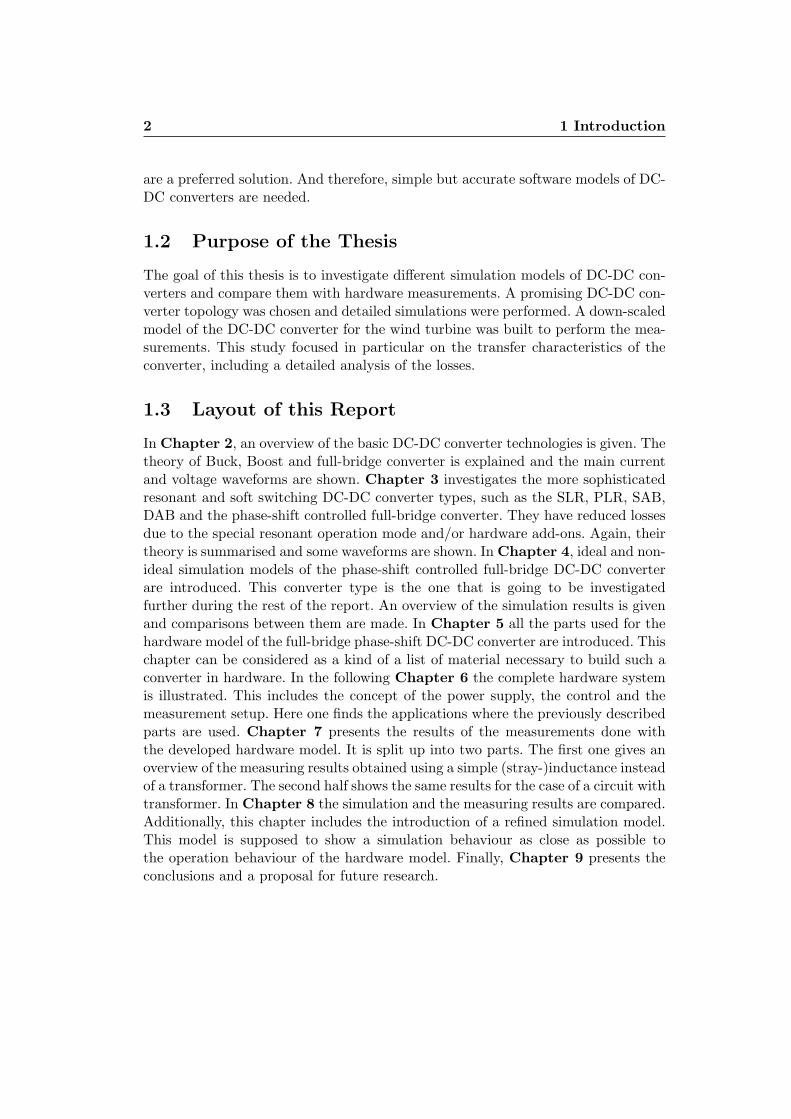
Figure 2.1: Buck Converter Schematics
Three of the most important topologies of the hard-switched DC-DC convertersare discussed in this chapter. These are the Buck, the Boost and the full-bridgeconverter.
2.1 Buck (Step-Down) Converter
A Buck converter is a so-called step-down converter. This means that a DC inputvoltage is stepped down to a lower voltage at the output stage. The circuit infigure 2.1 shows such a Buck converter. It delivers pulses of current to the outputby being in one of the two switch-states, on or off. During the on-state the dioded becomes reverse biased and the input provides energy to the load and to theinductor L, where it is stored. During the off-state, the inductor is discharging itsstored energy to the load. The capacitor C provides a stable voltage across theoutput load. When the inductor has discharged, its current iLs falls towards zeroand even tends to reverse, but the diode blocks conduction in the reverse direction.If the current goes to zero, a third state is reached. This state only exists in aspecial operation mode called discontinuous-conduction mode (DCM) (see followingparagraphs), where both the diode and the switch are off.
Consequently, the operation of a Buck converter can be divided into the follow-ing two different conduction modes: continuous-conduction mode and discontinuous-conduction mode:
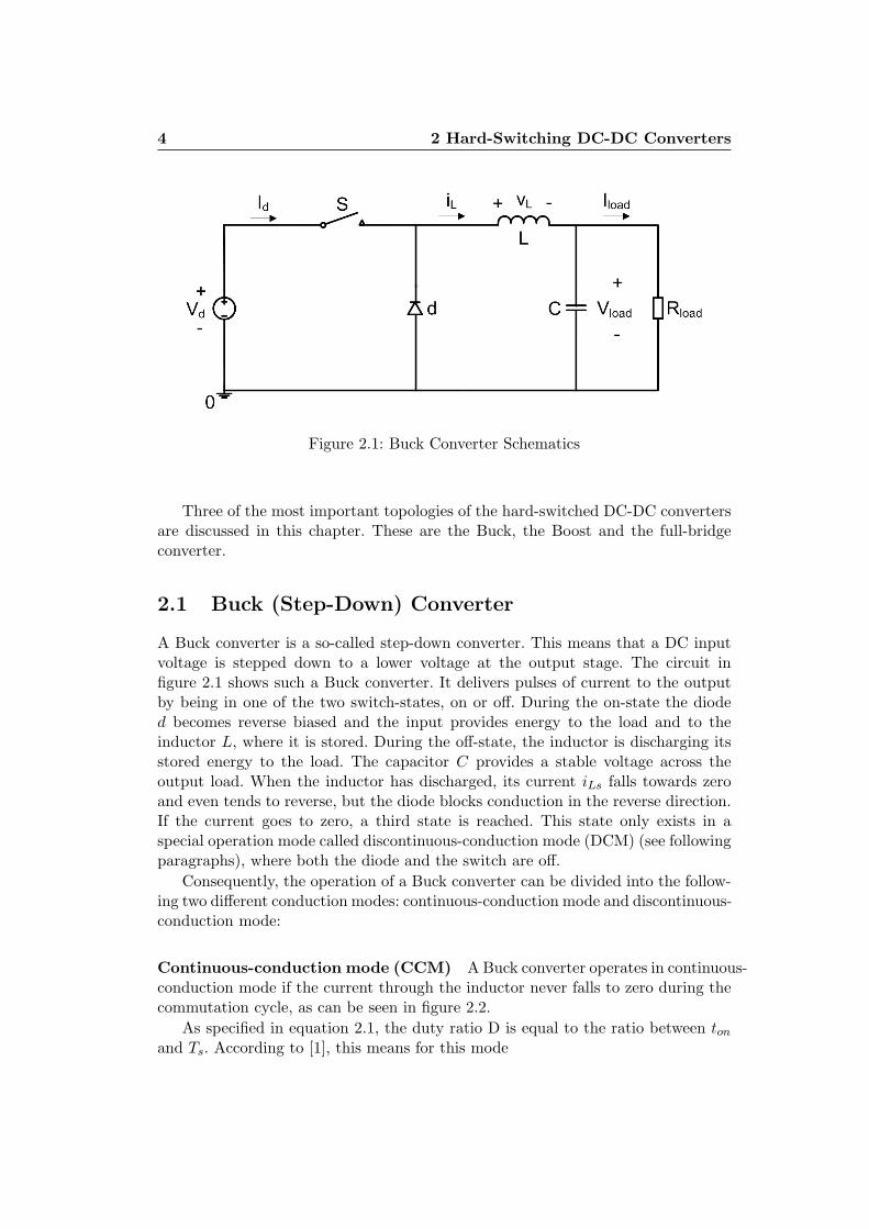
Continuous-conduction mode (CCM) A Buck converter operates in continuous-conduction mode if the current through the inductor never falls to zero during thecommutation cycle, as can be seen in figure 2.2.
As specified in equation 2.1, the duty ratio D is equal to the ratio between ton
and Ts. According to [1], this means for this mode
2.1 Buck (Step-Down) Converter 5
Figure 2.2: Voltage and Current Waveforms of a Buck Converter in CCM
D =ton
Ts=
Vload
Vd, (2.2)
where Vd is the DC input voltage and Vload the desired output voltage. Neglect-ing power losses associated with all the circuit elements, the input power Pd = VdId
equals the output power P0 = VloadIload. Therefore,
Iload
Id=
Vd
Vload=
1D
. (2.3)
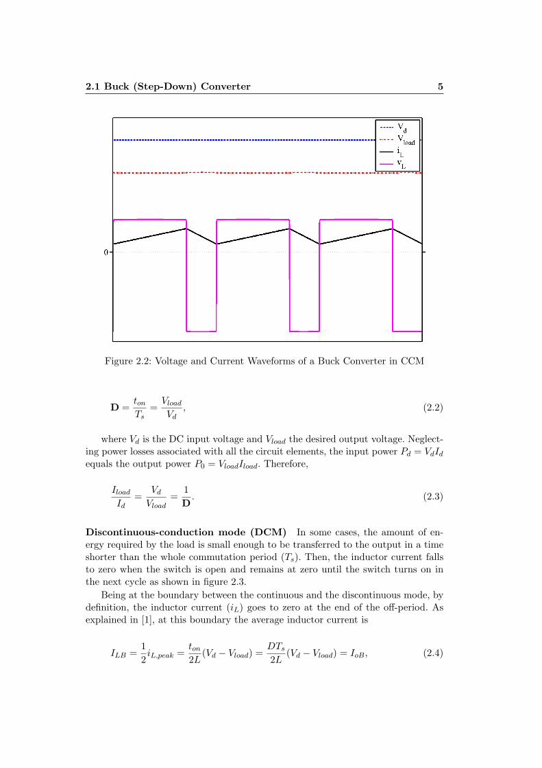
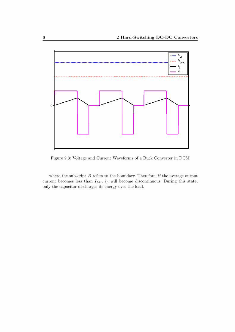
Discontinuous-conduction mode (DCM) In some cases, the amount of en-ergy required by the load is small enough to be transferred to the output in a timeshorter than the whole commutation period (Ts). Then, the inductor current fallsto zero when the switch is open and remains at zero until the switch turns on inthe next cycle as shown in figure 2.3.
Being at the boundary between the continuous and the discontinuous mode, bydefinition, the inductor current (iL) goes to zero at the end of the off-period. Asexplained in [1], at this boundary the average inductor current is
ILB =12iL,peak =
ton
2L(Vd − Vload) =
DTs
2L(Vd − Vload) = IoB, (2.4)
6 2 Hard-Switching DC-DC Converters
Figure 2.3: Voltage and Current Waveforms of a Buck Converter in DCM
where the subscript B refers to the boundary. Therefore, if the average outputcurrent becomes less than ILB, iL will become discontinuous. During this state,only the capacitor discharges its energy over the load.
2.2 Boost (Step-Up) Converter 7
Figure 2.4: Boost Converter Schematics
2.2 Boost (Step-Up) Converter
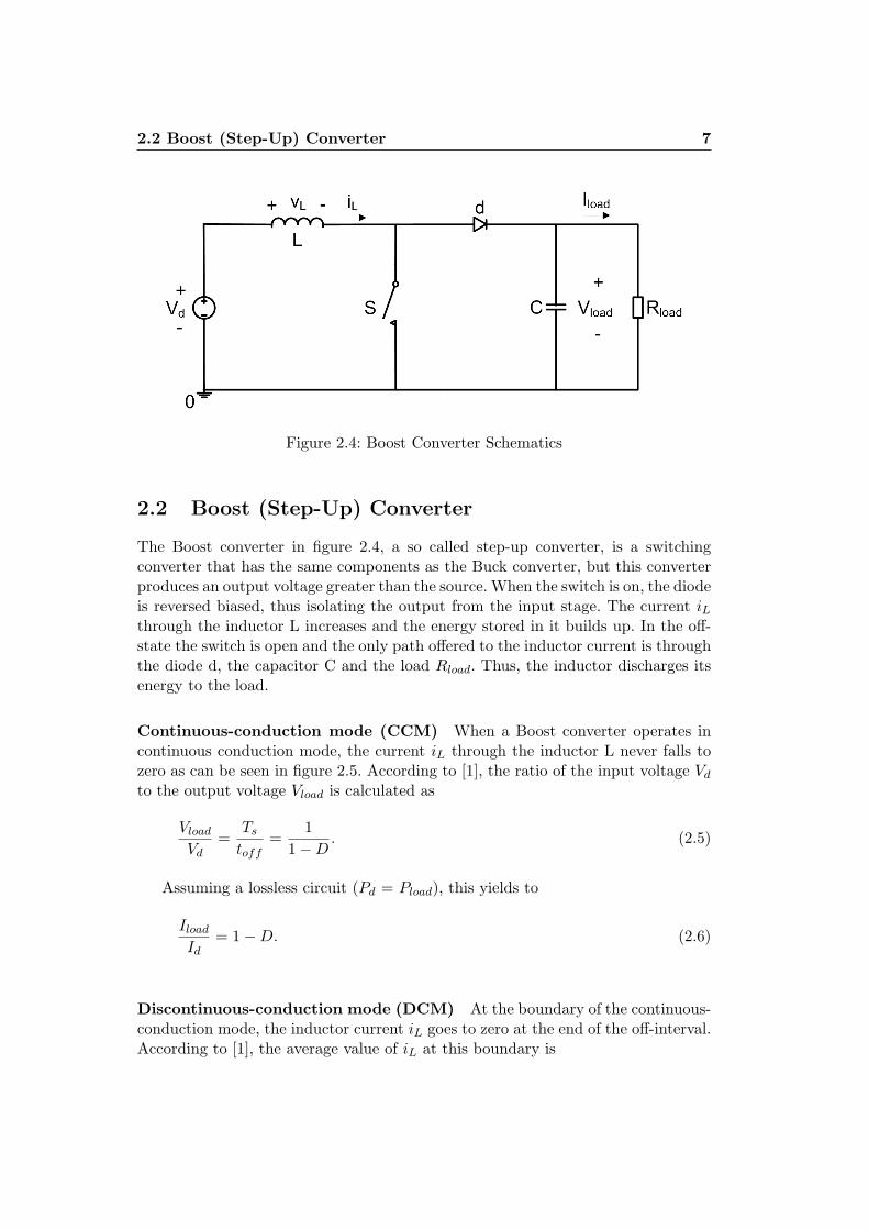
The Boost converter in figure 2.4, a so called step-up converter, is a switchingconverter that has the same components as the Buck converter, but this converterproduces an output voltage greater than the source. When the switch is on, the diodeis reversed biased, thus isolating the output from the input stage. The current iLthrough the inductor L increases and the energy stored in it builds up. In the off-state the switch is open and the only path offered to the inductor current is throughthe diode d, the capacitor C and the load Rload. Thus, the inductor discharges itsenergy to the load.
Continuous-conduction mode (CCM) When a Boost converter operates incontinuous conduction mode, the current iL through the inductor L never falls tozero as can be seen in figure 2.5. According to [1], the ratio of the input voltage Vd
to the output voltage Vload is calculated as
Vload
Vd=
Ts
toff=
11−D
. (2.5)
Assuming a lossless circuit (Pd = Pload), this yields to
Iload
Id= 1−D. (2.6)
Discontinuous-conduction mode (DCM) At the boundary of the continuous-conduction mode, the inductor current iL goes to zero at the end of the off-interval.According to [1], the average value of iL at this boundary is
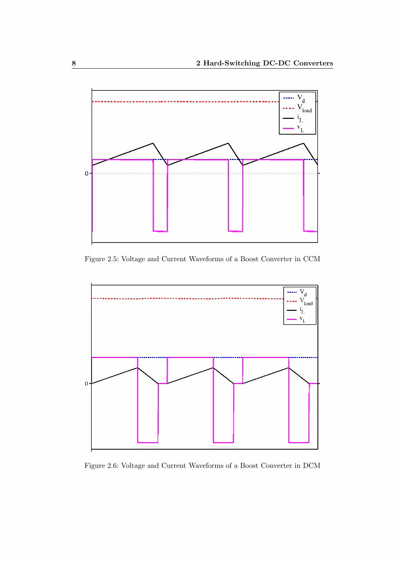
8 2 Hard-Switching DC-DC Converters
Figure 2.5: Voltage and Current Waveforms of a Boost Converter in CCM
Figure 2.6: Voltage and Current Waveforms of a Boost Converter in DCM

2.2 Boost (Step-Up) Converter 9
ILB =TsVload
2LD(1−D). (2.7)
Figure 2.6 shows the current through the inductor falling to zero during partsof the period Ts in the discontinuous mode. The only difference compared to theprinciple of the continuous mode is, that the inductor is completely discharged atthe end of the commutation cycle.

10 2 Hard-Switching DC-DC Converters
2.3 Full-Bridge DC-DC Converter
Figure 2.7: Full-Bridge Converter Schematics
Unlike the previously discussed Buck and Boost converters, the full-bridge DC-DC converter contains four switches and a transformer to achieve the desired outputvoltage level. Furthermore, it belongs to the primary switched converter family sincethere is isolation between input and output.
The input stage of the converter supplies the high-frequency transformer with anAC voltage vp, where the negative as well as the positive half-wave transfer energy.The primary transformer voltage vp = vAB can be +Vd, -Vd or zero depending onwhich pair of transistors (S1, S4 or S2, S3) that are turned on or off. All the possiblestates of the switches and the corresponding values of vAN , vBN and vp can be seencombined in table 2.1.
Table 2.1: States of Switches, vAN , vBN and vp
S1 S2 S3 S4 vAN vBN vp
on off off on Vd 0 +Vd
off on on off 0 Vd -Vd
off off off off Vd Vd 0
On the secondary side, the AC voltage is rectified by the diode bridge. The low-pass filter finally produces a smooth DC output voltage. For continuous conductionmode (iL always greater than zero) this leads to
Vload = Vd(N2
N1)(
ton
Ts), (2.8)
where again ton is the on-duration of the switches and 1/Ts the switching fre-quency. Hence, ton/Ts is the duty cycle D in the PWM mode of operation as definedin equation 2.1 for the Buck converter. Figure 2.8 shows the waveforms of the most
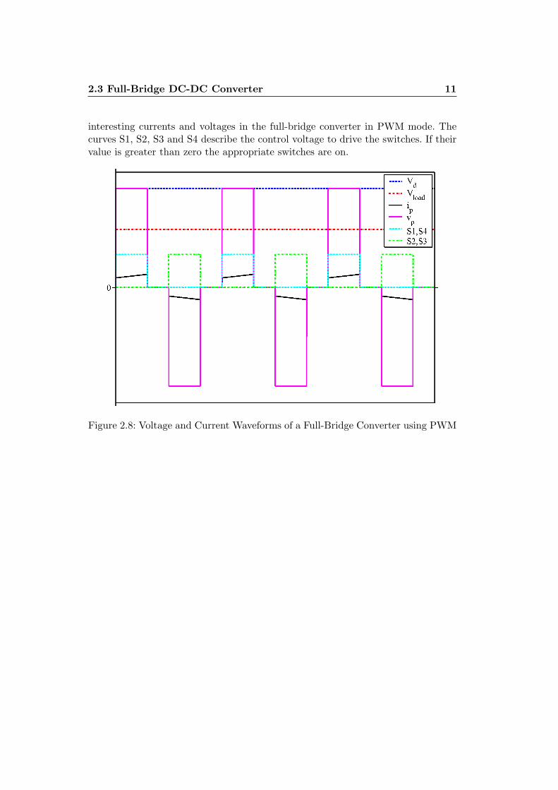
2.3 Full-Bridge DC-DC Converter 11
interesting currents and voltages in the full-bridge converter in PWM mode. Thecurves S1, S2, S3 and S4 describe the control voltage to drive the switches. If theirvalue is greater than zero the appropriate switches are on.
Figure 2.8: Voltage and Current Waveforms of a Full-Bridge Converter using PWM

Chapter 3
Resonant DC-DC Converters
When using hard-switching DC-DC converters, there are turn-on and turn-off lossesin the switches because the entire load current is switched on and off during eachoperation cycle. Therefore, the switches are subjected to high switching stress andhigh switching power loss. Another drawback is the EMI (electromagnetic interfer-ence) produced due to the large di/dt and dv/dt occurring due to hard-switching.In so-called soft-switching converters, the circuit is designed such that each switchin the converter changes its state when the voltage across it and/or the currentthrough it is zero at the switching instant. Most topologies require some form ofLC resonance in order to achieve this. These are classified as “resonant converters”.
It is possible to distinguish between “load-resonant” and “resonant-switch” con-verters. Load-resonant converters contain an LC resonant tank circuit. Voltage andcurrent oscillate due to the LC resonance of the tank. In that way, the converterswitches can be switched at zero voltage and/or zero current if the time constantsand the switching frequency are appropriately chosen.
In resonant-switch topologies however, resonant elements are used to shape thevoltage across the switch and/or the current through it. Usually, some kind ofsnubber circuits are used to achieve the intended voltage and current waveformsfor the switches. The most important representatives of these two converter classesare discussed in this chapter.
3.1 Load-Resonant Converters
As mentioned above, load-resonant converters contain an LC resonant tank circuit.Either a series LC or a parallel LC circuit can be used. In these converter circuits,the power flow to the load is controlled by the resonant tank impedance. This im-pedance in turn is controlled by the switching frequency ωs in comparison to theresonant frequency ω0 = 1√
LrCrof the tank [1].
14 3 Resonant DC-DC Converters
Modes of operation For load-resonant converters, there are three possible modesof operation based on the ratio of the switching frequency ωs to the resonant fre-quency ω0. This ratio determines whether the current through the inductor of theresonant tank iLr flows continuously or discontinuously [1]:
• Discontinuous-conduction mode (DCM): ωs < 12ω0
• Continuous-conduction mode (CCM): 12ω0 < ωs < ω0
• Continuous-conduction mode: ωs > ω0
3.1.1 Series-Loaded Resonant Converter (SLR)
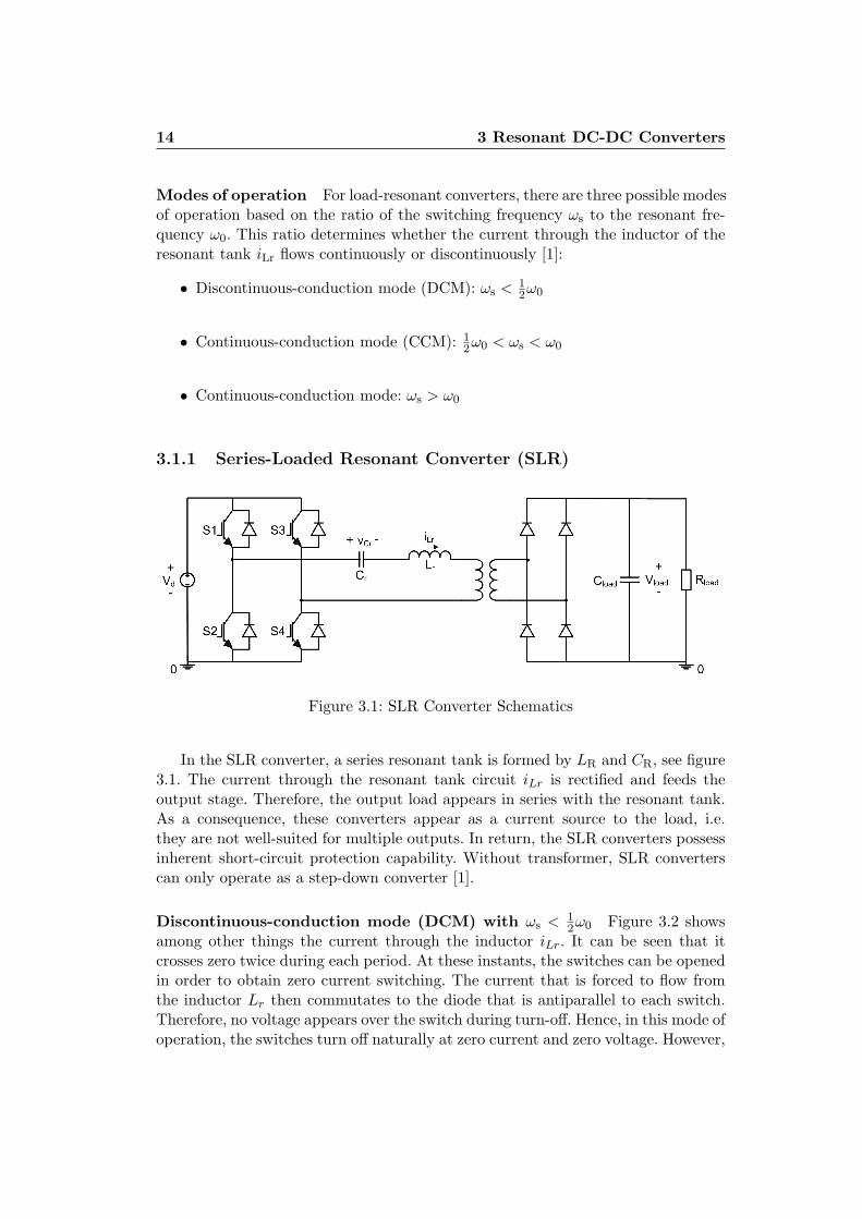
Figure 3.1: SLR Converter Schematics
In the SLR converter, a series resonant tank is formed by LR and CR, see figure3.1. The current through the resonant tank circuit iLr is rectified and feeds theoutput stage. Therefore, the output load appears in series with the resonant tank.As a consequence, these converters appear as a current source to the load, i.e.they are not well-suited for multiple outputs. In return, the SLR converters possessinherent short-circuit protection capability. Without transformer, SLR converterscan only operate as a step-down converter [1].
Discontinuous-conduction mode (DCM) with ωs < 12ω0 Figure 3.2 shows
among other things the current through the inductor iLr. It can be seen that itcrosses zero twice during each period. At these instants, the switches can be openedin order to obtain zero current switching. The current that is forced to flow fromthe inductor Lr then commutates to the diode that is antiparallel to each switch.Therefore, no voltage appears over the switch during turn-off. Hence, in this mode ofoperation, the switches turn off naturally at zero current and zero voltage. However,
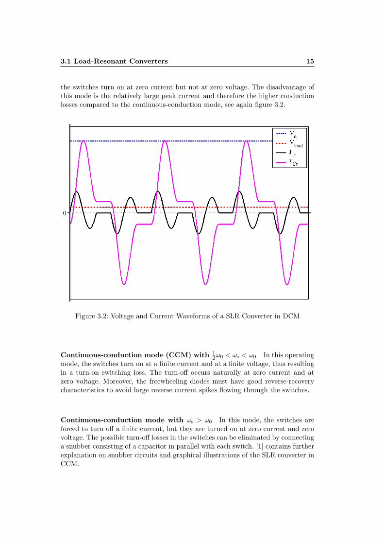
3.1 Load-Resonant Converters 15
the switches turn on at zero current but not at zero voltage. The disadvantage ofthis mode is the relatively large peak current and therefore the higher conductionlosses compared to the continuous-conduction mode, see again figure 3.2.
Figure 3.2: Voltage and Current Waveforms of a SLR Converter in DCM
Continuous-conduction mode (CCM) with 12ω0 < ωs < ω0 In this operating
mode, the switches turn on at a finite current and at a finite voltage, thus resultingin a turn-on switching loss. The turn-off occurs naturally at zero current and atzero voltage. Moreover, the freewheeling diodes must have good reverse-recoverycharacteristics to avoid large reverse current spikes flowing through the switches.
Continuous-conduction mode with ωs > ω0 In this mode, the switches areforced to turn off a finite current, but they are turned on at zero current and zerovoltage. The possible turn-off losses in the switches can be eliminated by connectinga snubber consisting of a capacitor in parallel with each switch. [1] contains furtherexplanation on snubber circuits and graphical illustrations of the SLR converter inCCM.

16 3 Resonant DC-DC Converters
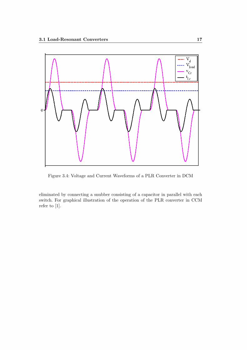
3.1.2 Parallel-Loaded Resonant Converter (PLR)
Figure 3.3: PLR Converter Schematics
PLR converters are similar to the SLR converters in terms of operating witha series-resonant LC tank circuit. However, unlike the SLR converters, the outputstage is connected in parallel with the resonant-tank capacitor Cr. Therefore, PLRconverters appear as a voltage source and hence, are better suited for multipleoutputs than SLR converters. Additionally, PLR converters are able to operate asstep-up as well as step-down converters. But they do not possess inherent short-circuit protection. Another drawback of this converter type lies in the fact that thepeak inductor current and peak capacitor voltage can be several times higher thanthe load current Iload and the input voltage Vd, respectively [1].
Discontinuous mode of operation with ωs < 12ω0 In this mode of operation,
both vCr and iLr stay at zero for an interval that can be varied in order to controlthe output voltage, see figure 3.4. The output power varies linearly with ωS andVload remains independent of Iload. In addition, there are no turn-on or turn-offstresses on the switches or diodes.
Continuous mode of operation (DCM) with 12ω0 < ωs < ω0 There are
turn-on losses in this operating mode, because both vCr and iLr become continuous.Additionally, the diodes must have good reverse-recovery characteristics. However,there are no turn-off losses in the switches since the current through them commu-tates naturally to the antiparallel diodes when iLr reverses in direction.
Continuous mode of operation (CCM) with ωs > ω0 Here, the turn-onlosses are eliminated since the switches turn on naturally when iLr (initially flowingthrough the diodes) reverses. Yet, there are turn-off losses in the switches since aswitch is forced to turn off, thus transferring its current to the diode connected inantiparallel with the other switch. Similar to SLR converters, these losses can be
3.1 Load-Resonant Converters 17
Figure 3.4: Voltage and Current Waveforms of a PLR Converter in DCM
eliminated by connecting a snubber consisting of a capacitor in parallel with eachswitch. For graphical illustration of the operation of the PLR converter in CCMrefer to [1].
18 3 Resonant DC-DC Converters
3.1.3 Hybrid-Resonant converters
Hybrid-resonant DC-DC converters combine or enhance the characteristics of SLRand/or PLR converters. There are several hybrid-resonant converter topologies,such as LCC, LLC and LCL. In this thesis however, only the LCC converter isconsidered.
3.1.3.1 The Series Parallel Resonant Converter (LCC)
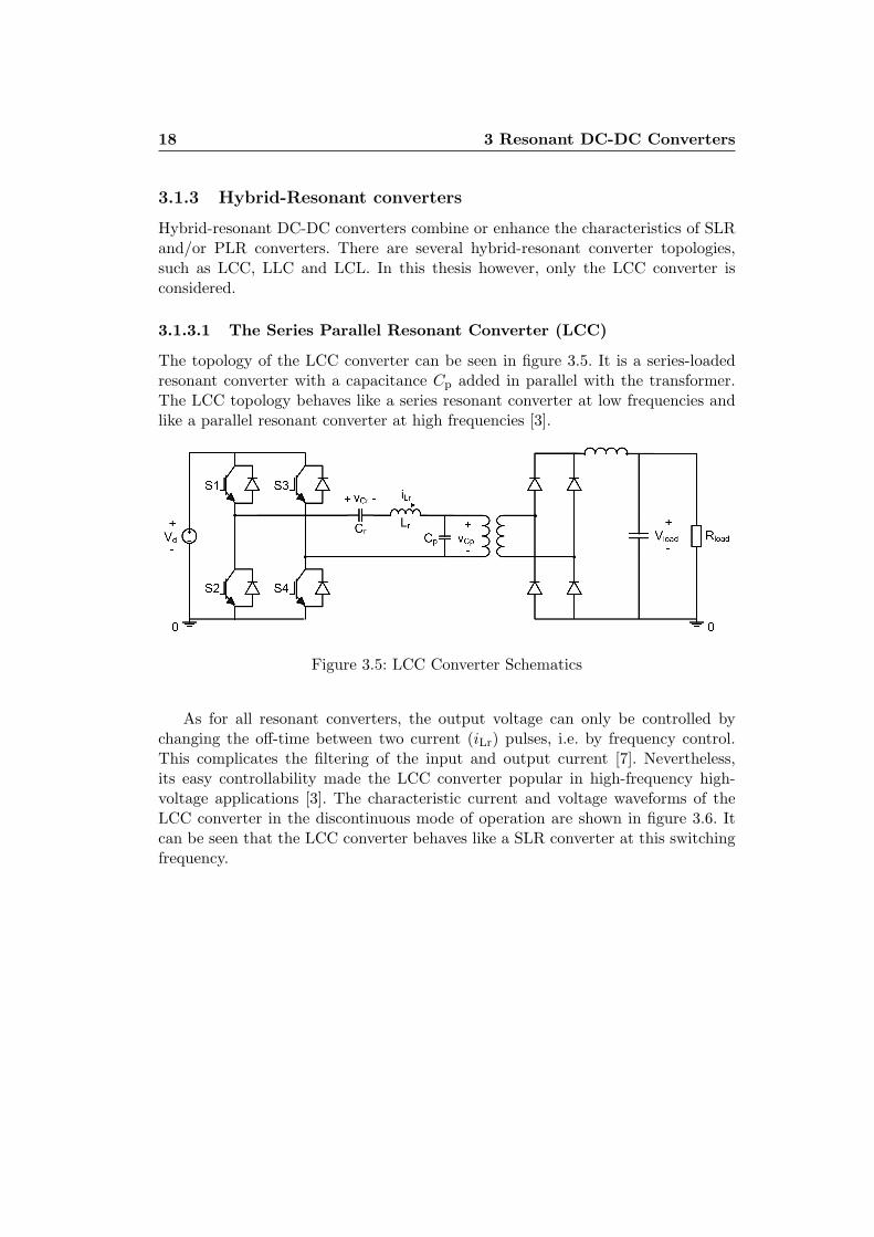
The topology of the LCC converter can be seen in figure 3.5. It is a series-loadedresonant converter with a capacitance Cp added in parallel with the transformer.The LCC topology behaves like a series resonant converter at low frequencies andlike a parallel resonant converter at high frequencies [3].
Figure 3.5: LCC Converter Schematics
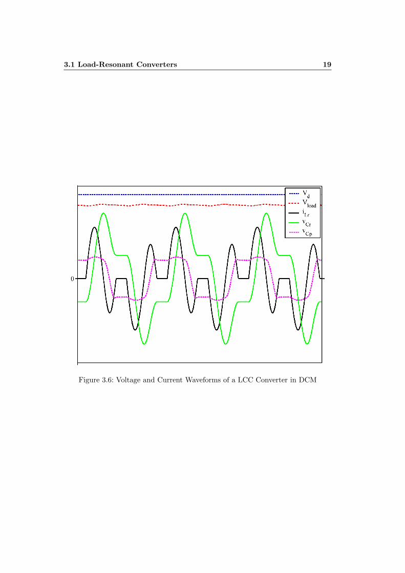
As for all resonant converters, the output voltage can only be controlled bychanging the off-time between two current (iLr) pulses, i.e. by frequency control.This complicates the filtering of the input and output current [7]. Nevertheless,its easy controllability made the LCC converter popular in high-frequency high-voltage applications [3]. The characteristic current and voltage waveforms of theLCC converter in the discontinuous mode of operation are shown in figure 3.6. Itcan be seen that the LCC converter behaves like a SLR converter at this switchingfrequency.
3.1 Load-Resonant Converters 19
Figure 3.6: Voltage and Current Waveforms of a LCC Converter in DCM
20 3 Resonant DC-DC Converters
3.2 Resonant-Switch Converters
In certain switch-mode converter topologies, a LC resonance can be utilised pri-marily to shape the switch voltage and current to provide zero-voltage and/or zero-current switchings. Often, inductors (such as the transformer stray inductance1)and capacitors (such as the output capacitance of the semiconductor switch) thatappear as undesirable parasitics in switch-mode topologies can be utilised to providethe resonant inductor and the capacitor needed for the resonant-switch circuit.In resonant-switch converters, during one switching-frequency time period, thereare resonant as well as non-resonant operating intervals. Sometimes these convert-ers are also referred to as “quasi-resonant converters” [1].
Zero-Current-Switching Converters (ZCS) As the name suggests, the switchesturn on and off at zero current in this type of topology.
Zero-Voltage-Switching Converters (ZVS) Here, the switches turn on andoff at zero voltage. In general, ZVS is preferable to ZCS at high switching frequenciesbecause of the lower losses of switching at zero voltage [1].
3.2.1 Single Active Bridge (SAB)
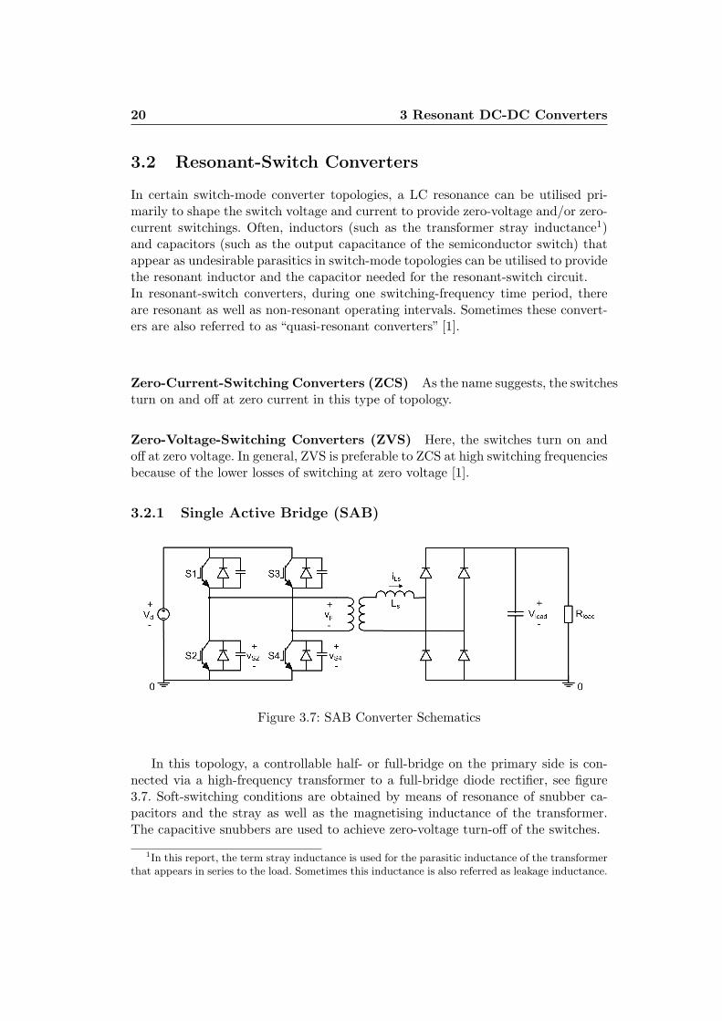
Figure 3.7: SAB Converter Schematics
In this topology, a controllable half- or full-bridge on the primary side is con-nected via a high-frequency transformer to a full-bridge diode rectifier, see figure3.7. Soft-switching conditions are obtained by means of resonance of snubber ca-pacitors and the stray as well as the magnetising inductance of the transformer.The capacitive snubbers are used to achieve zero-voltage turn-off of the switches.
1In this report, the term stray inductance is used for the parasitic inductance of the transformerthat appears in series to the load. Sometimes this inductance is also referred as leakage inductance.
3.2 Resonant-Switch Converters 21
The advantage of this topology lies in its simplicity and its easy controllabilityin constant frequency operation. However, the output diodes are hard-switched andthere can be an interaction between the stray inductance and the output rectifier[2]. Additionally, it is shown in [7] that the average losses of the SAB converter arenoticeably higher than in other converter configurations.
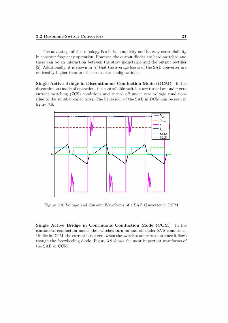
Single Active Bridge in Discontinuous Conduction Mode (DCM) In thediscontinuous mode of operation, the controllable switches are turned on under zerocurrent switching (ZCS) conditions and turned off under zero voltage conditions(due to the snubber capacitors). The behaviour of the SAB in DCM can be seen infigure 3.8.
Figure 3.8: Voltage and Current Waveforms of a SAB Converter in DCM
Single Active Bridge in Continuous Conduction Mode (CCM) In thecontinuous conduction mode, the switches turn on and off under ZVS conditions.Unlike in DCM, the current is not zero when the switches are turned on since it flowsthough the freewheeling diode. Figure 3.9 shows the most important waveforms ofthe SAB in CCM.
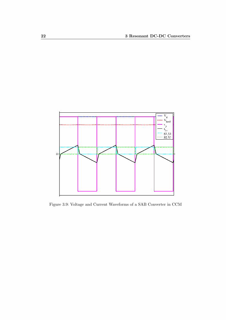
22 3 Resonant DC-DC Converters
Figure 3.9: Voltage and Current Waveforms of a SAB Converter in CCM
3.2 Resonant-Switch Converters 23
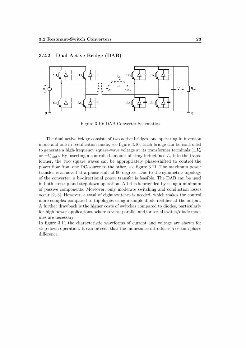
3.2.2 Dual Active Bridge (DAB)
Figure 3.10: DAB Converter Schematics
The dual active bridge consists of two active bridges, one operating in inversionmode and one in rectification mode, see figure 3.10. Each bridge can be controlledto generate a high-frequency square-wave voltage at its transformer terminals (±Vd
or ±Vload). By inserting a controlled amount of stray inductance Ls into the trans-former, the two square waves can be appropriately phase-shifted to control thepower flow from one DC-source to the other, see figure 3.11. The maximum powertransfer is achieved at a phase shift of 90 degrees. Due to the symmetric topologyof the converter, a bi-directional power transfer is feasible. The DAB can be usedin both step-up and step-down operation. All this is provided by using a minimumof passive components. Moreover, only moderate switching and conduction lossesoccur [2, 3]. However, a total of eight switches is needed, which makes the controlmore complex compared to topologies using a simple diode rectifier at the output.A further drawback is the higher costs of switches compared to diodes, particularlyfor high power applications, where several parallel and/or serial switch/diode mod-ules are necessary.In figure 3.11 the characteristic waveforms of current and voltage are shown forstep-down operation. It can be seen that the inductance introduces a certain phasedifference.
24 3 Resonant DC-DC Converters
Figure 3.11: Voltage and Current Waveforms of a DAB Converter in Step-DownOperation

3.2 Resonant-Switch Converters 25
3.2.3 Full-Bridge DC-DC Converter with Phase-Shift Control
Figure 3.12: Phase-Shift Controlled Full-Bridge Schematics
It is possible to operate a full-bridge DC-DC converter under ZVS conditionsby using circuit parasitics to obtain resonant switching. To this end, a phase dif-ference between the two half-bridge switch networks is inserted. Both halves of thebridge switch network operate with 50% duty cycle D and the phase-shift is variedto control the output voltage [6]. A schematic overview of the converter is given infigure 3.12.
The driving signals for the switches S1 to S4 are such that, instead of turning onthe diagonally opposite switches in the bridge simultaneously (as in the full-bridgethat uses PWM), a delay time TD is introduced between the turn-on instants of theswitches in the right leg (S4 and S3) and the ones in the left leg (S1 and S2).
In [6] the so-called phase-shift variable φ is defined as
φ =(t1 − t0)
Ts/2(3.1)
This phase shift determines the operation duty cycle of the converter. Figure3.13 illustrates the definition of φ and TD
2. It is obvious that the phase-shift vari-able φ lies in a range 0 ≤ φ ≤ 1.
According to [6], the volt-second balance on the secondary-side filter inductorLf can be expressed as
Vload(1− φ)(Ts
2) = (nVd − Vload)φ(
Ts
2). (3.2)
2In figure 3.13, the control signals for the switches S1 and S4 as well as S2 and S3 are shownwith different amplitudes for clarity reasons. In reality however, the switch control signals have thesame amplitude.
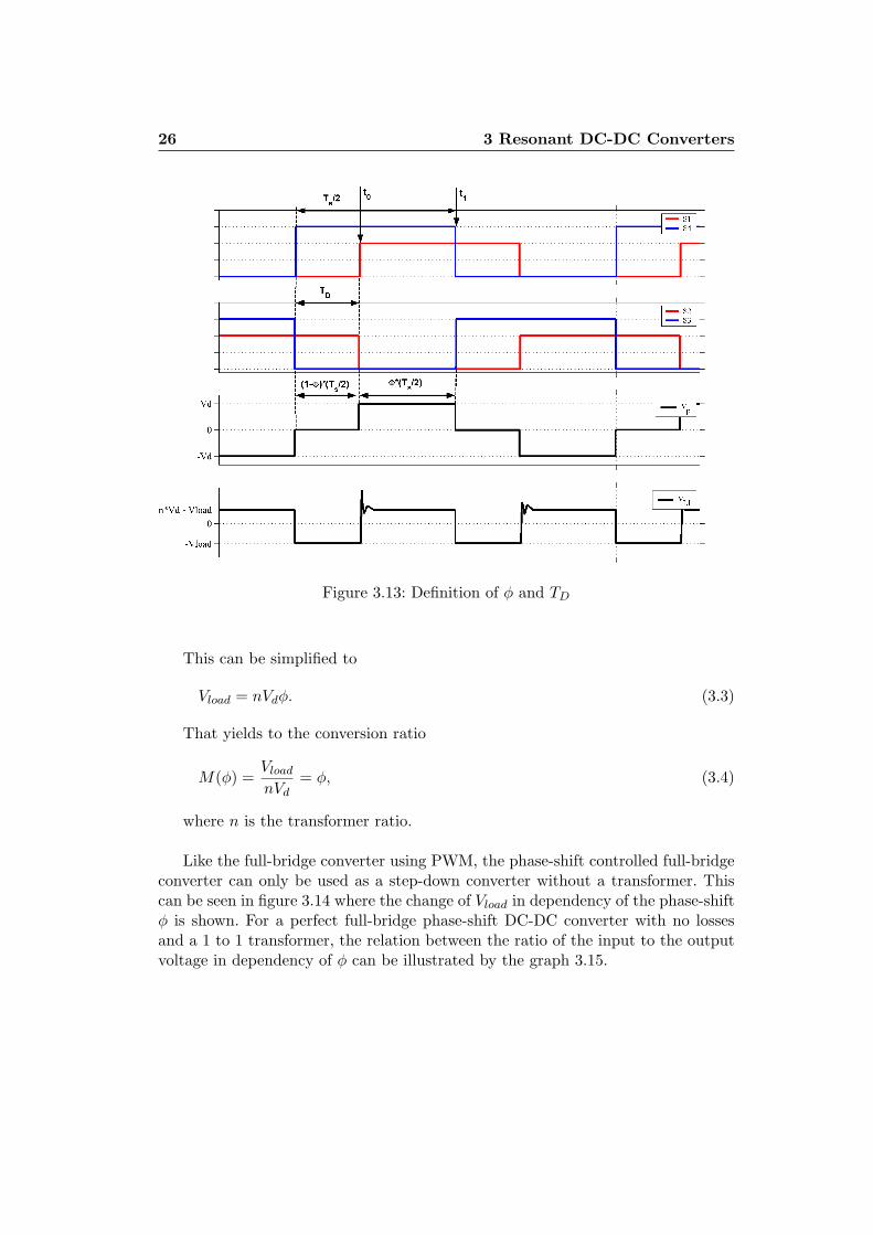
26 3 Resonant DC-DC Converters
Figure 3.13: Definition of φ and TD
This can be simplified to
Vload = nVdφ. (3.3)
That yields to the conversion ratio
M(φ) =Vload
nVd= φ, (3.4)
where n is the transformer ratio.
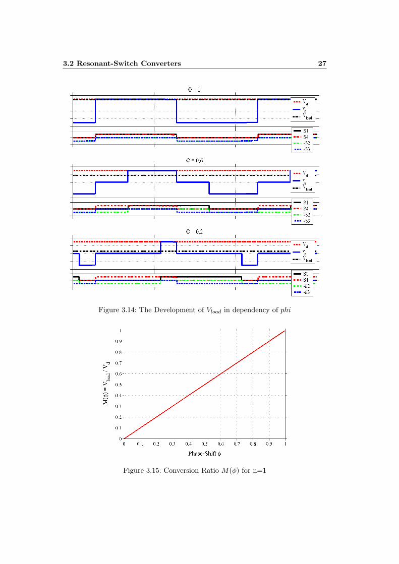
Like the full-bridge converter using PWM, the phase-shift controlled full-bridgeconverter can only be used as a step-down converter without a transformer. Thiscan be seen in figure 3.14 where the change of Vload in dependency of the phase-shiftφ is shown. For a perfect full-bridge phase-shift DC-DC converter with no lossesand a 1 to 1 transformer, the relation between the ratio of the input to the outputvoltage in dependency of φ can be illustrated by the graph 3.15.
3.2 Resonant-Switch Converters 27
Figure 3.14: The Development of Vload in dependency of phi
Figure 3.15: Conversion Ratio M(φ) for n=1
28 3 Resonant DC-DC Converters
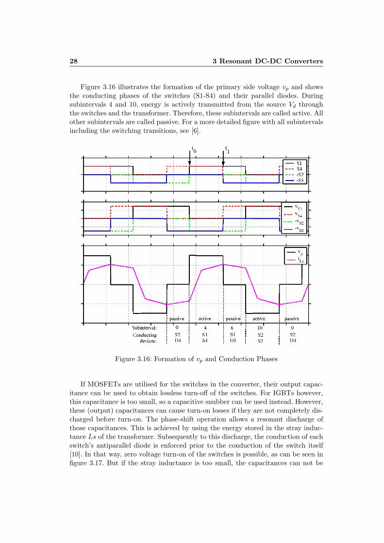
Figure 3.16 illustrates the formation of the primary side voltage vp and showsthe conducting phases of the switches (S1-S4) and their parallel diodes. Duringsubintervals 4 and 10, energy is actively transmitted from the source Vd throughthe switches and the transformer. Therefore, these subintervals are called active. Allother subintervals are called passive. For a more detailed figure with all subintervalsincluding the switching transitions, see [6].
Figure 3.16: Formation of vp and Conduction Phases
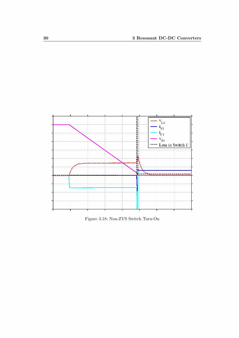
If MOSFETs are utilised for the switches in the converter, their output capac-itance can be used to obtain lossless turn-off of the switches. For IGBTs however,this capacitance is too small, so a capacitive snubber can be used instead. However,these (output) capacitances can cause turn-on losses if they are not completely dis-charged before turn-on. The phase-shift operation allows a resonant discharge ofthose capacitances. This is achieved by using the energy stored in the stray induc-tance Ls of the transformer. Subsequently to this discharge, the conduction of eachswitch’s antiparallel diode is enforced prior to the conduction of the switch itself[10]. In that way, zero voltage turn-on of the switches is possible, as can be seen infigure 3.17. But if the stray inductance is too small, the capacitances can not be
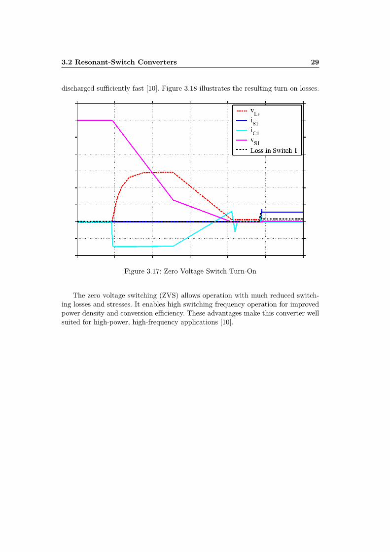
3.2 Resonant-Switch Converters 29
discharged sufficiently fast [10]. Figure 3.18 illustrates the resulting turn-on losses.
Figure 3.17: Zero Voltage Switch Turn-On
The zero voltage switching (ZVS) allows operation with much reduced switch-ing losses and stresses. It enables high switching frequency operation for improvedpower density and conversion efficiency. These advantages make this converter wellsuited for high-power, high-frequency applications [10].
30 3 Resonant DC-DC Converters
Figure 3.18: Non-ZVS Switch Turn-On
Chapter 4
Simulations
In this thesis, simulations were performed with all DC-DC converter topologiesmentioned in the previous chapters. However, the phase-shift controlled full-bridgeconverter was chosen to be investigated further due to its simplicity and its lowlosses during operation, see [7]. It is also this topology that is implemented in hard-ware in a later stage of this thesis. Therefore, the full-bridge phase-shift controlledconverter was investigated in detail using simulations with the simulation softwarePSpice. This chapter explains the simulation models that were elaborated and givesan overview of the results that were obtained.
4.1 Simulation Circuit Implementations
In this section it is shown how the phase-shift controlled full-bridge converter wasimplemented for the simulations. The intention was to build a software model asclose as possible to the hardware model used in a later stage of this thesis. PSpiceoffers a large number of part-libraries. Additionally to the ideal parts, several li-braries of different manufacturers providing non-ideal parts are available. In a firststep, the simulation circuit was built with ideal parts only. After this, in order tomake the simulations as realistic as possible, the parts that were assumed to showthe greatest deviations from the ideal case during operation were replaced by theirnon-ideal counterparts.
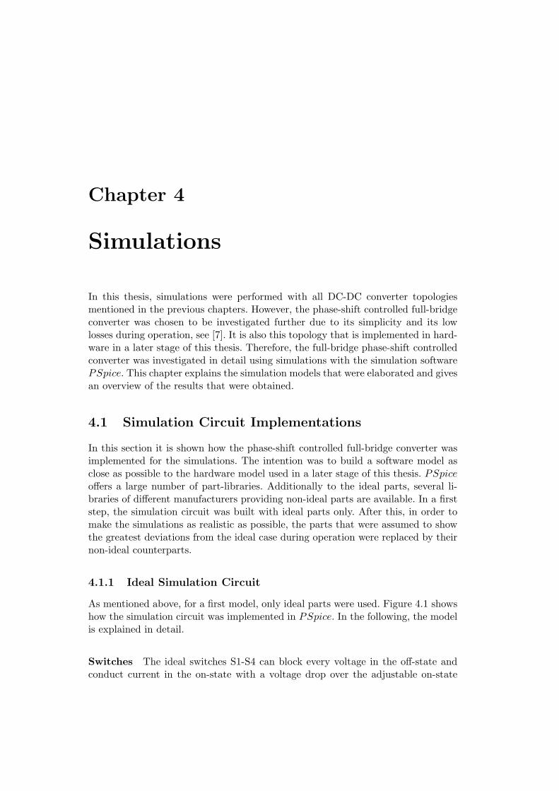
4.1.1 Ideal Simulation Circuit
As mentioned above, for a first model, only ideal parts were used. Figure 4.1 showshow the simulation circuit was implemented in PSpice. In the following, the modelis explained in detail.
Switches The ideal switches S1-S4 can block every voltage in the off-state andconduct current in the on-state with a voltage drop over the adjustable on-state
32 4 Simulations
Figure 4.1: Ideal Simulation Circuit
resistance ron (here: 1mΩ). The required control signals are generated by four pulse-generators V1-V4. To adjust the phase-shift, the delay time TD of pulse generatorV1 and V2 have to be changed. This variable describes the delay between the risingedge of the to diagonally opposite control signals, see figure 3.13. The values of TDfrom V3 and V4 do not have to be changed. For V1 the modification of φ on thebasis of TD can be calculated with formula 4.1. For V2 a constant of 0.5/FS hasto be added to TD of V1.
φ =(t1 − t0)
Ts/2=
(Ts/2− TD)Ts/2
= 1− TD
Ts/2= 1− TD
0.5ms(4.1)
Transformer The real transformer used later in this thesis work does not changethe voltage level from the primary to the secondary side. It only provides galvanicseparation of the switches and the diode rectifier bridge. Therefore, the ideal simu-lation circuit was built without any transformer. Only the stray inductance Ls wasincluded because it is necessary for the desired switching performance. The otherparasitic components of a transformer were not considered for this ideal model.
Rectifier The rectifier bridge on the output stage of the DC-DC converter wasimplemented with four ideal diodes. Similarly to the ideal switches, they are ableto block every reverse voltage. Under forward voltage they conduct current with a

4.1 Simulation Circuit Implementations 33
voltage drop of 1V which is not current dependent. In order to avoid convergenceproblems during simulation, 10kΩ resistors were inserted in parallel with each diodeof the rectifier
To be able to compare the simulation and the measurement results in a laterstage of the thesis, the values of the simulation-parts are chosen identical to thehardware model parts. They can be seen in table 4.1.
Table 4.1: Ideal Simulation Parameters
Label Value Unit DescriptionVd 300 V input voltageFs 1 kHz switching frequencyC1 − C4 2.25 nF switch output capacitanceLs 10 µH transformer stray inductanceRload 5.3 Ω load resistanceCload 3300 µF load capacitanceLload 20 mH load inductance
34 4 Simulations
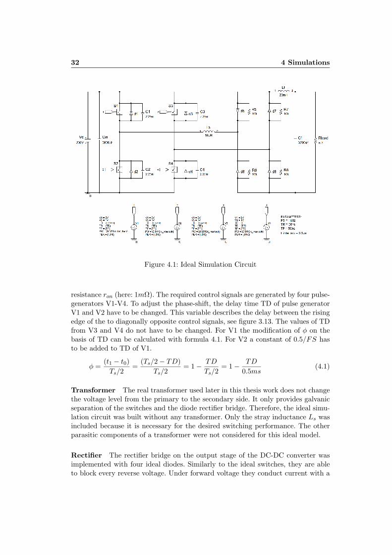
4.1.2 Non-Ideal Simulation Circuit
Figure 4.2: Non-Ideal Simulation Circuit
Some parts in the simulation model had to be replaced compared to the idealmodel used before to make simulations more close to reality. The parts that areintroduced for the non-ideal model are listed in this section. The final version of thenon-ideal simulation circuit can be seen in figure 4.2. The boxes control block 1−4and non ideal switch 1− 4 contain the IGBTs and the driver circuits.
IGBT The IGBT used for the measurements (SemikronSemix302GB 128D) isnot available in the PSpice library, so a representative was chosen (PowerexCM400HA − 24H). Those two IGBTs have comparable characteristics. Refer to the CDenclosed with this report for the two datasheets or to www.datasheetarchive.com.
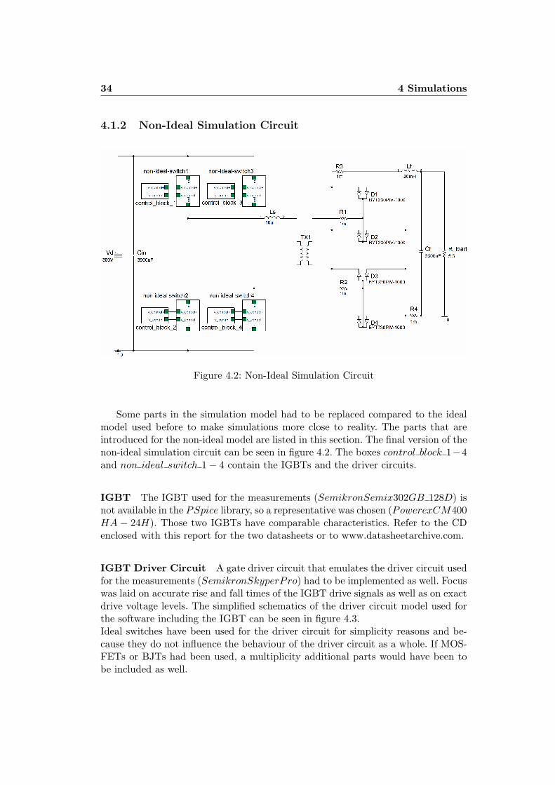
IGBT Driver Circuit A gate driver circuit that emulates the driver circuit usedfor the measurements (SemikronSkyperPro) had to be implemented as well. Focuswas laid on accurate rise and fall times of the IGBT drive signals as well as on exactdrive voltage levels. The simplified schematics of the driver circuit model used forthe software including the IGBT can be seen in figure 4.3.Ideal switches have been used for the driver circuit for simplicity reasons and be-cause they do not influence the behaviour of the driver circuit as a whole. If MOS-FETs or BJTs had been used, a multiplicity additional parts would have been tobe included as well.
4.1 Simulation Circuit Implementations 35
Figure 4.3: Software Driver Schematics
Transformer Model The Transformer used for the hardware setup was custom-made by an external company for the purpose of this application. Since the exactbehaviour was not known, an ideal transformer model together with an externalstray inductor was chosen and their values adjusted.
Diodes The ideal diodes for the output rectifier bridge were also replaced bythe diodes used for the measurements (ThomsonMicroelectronics BY T230PIV −1000). They can conduct 30A each, so always two of them were connected in parallelto be able to handle the maximum output current of 50A. The PSpice built-inlibraries do not provide a model for them by default. Therefore, a library wasdownloaded from the manufacturer home page. The library can be found on theCD to this report or on www.st.com.
For reasons that are not obvious to the authors, it is not possible to access thevoltages and the currents of this diodes directly in the simulations. So the 1mΩresistances R1-R4 were included in order to be able to monitor the behaviour ofthe diode rectifier bridge.
36 4 Simulations
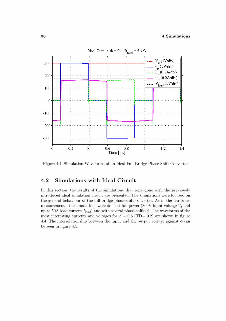
Figure 4.4: Simulation Waveforms of an Ideal Full-Bridge Phase-Shift Converter
4.2 Simulations with Ideal Circuit
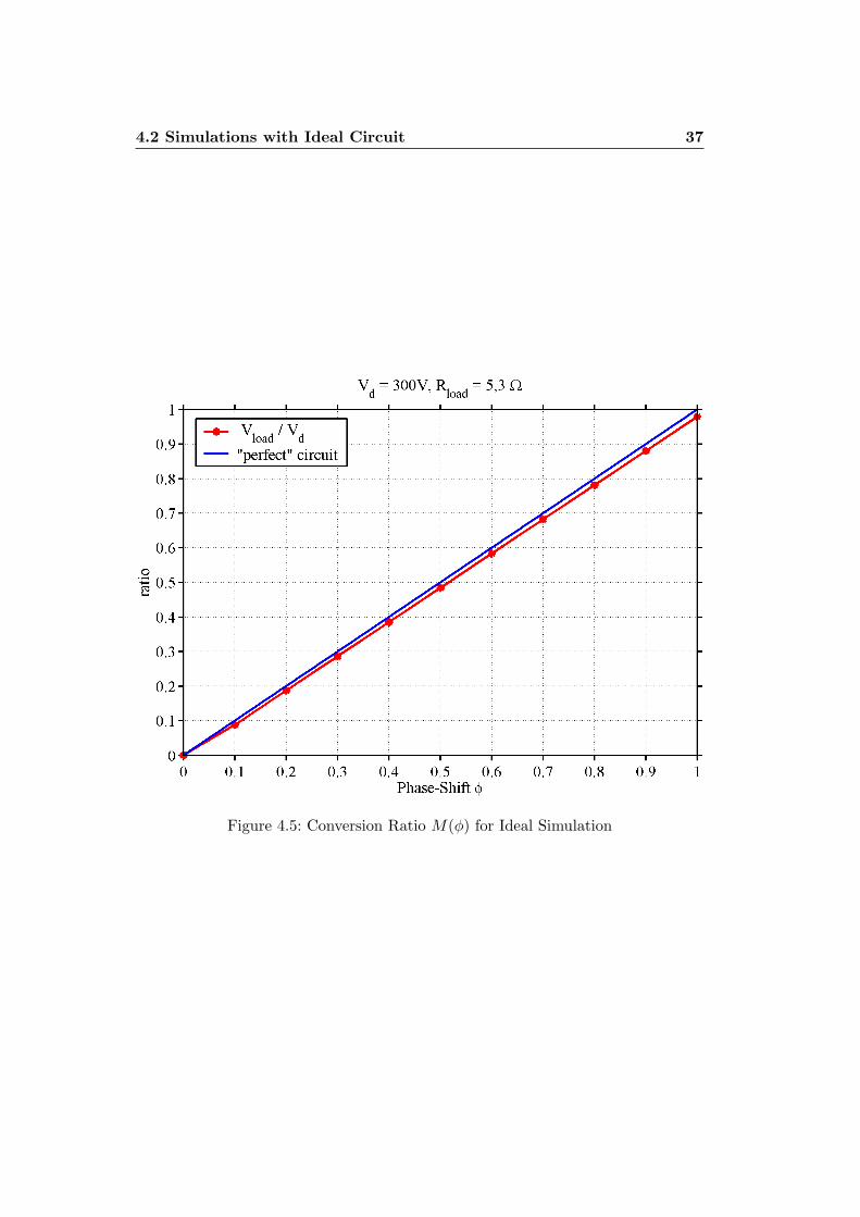
In this section, the results of the simulations that were done with the previouslyintroduced ideal simulation circuit are presented. The simulations were focused onthe general behaviour of the full-bridge phase-shift converter. As in the hardwaremeasurements, the simulations were done at full power (300V input voltage Vd andup to 50A load current Iload) and with several phase-shifts φ. The waveforms of themost interesting currents and voltages for φ = 0.6 (TD= 0.2) are shown in figure4.4. The interrelationship between the input and the output voltage against φ canbe seen in figure 4.5.
4.2 Simulations with Ideal Circuit 37
Figure 4.5: Conversion Ratio M(φ) for Ideal Simulation

38 4 Simulations
4.2.1 Interpretation of the Ideal-Simulation Results
There is a deviation of the simulation results gained with the ideal circuit elementscompared to what one would expect using the formula Vload = nφVd. The inter-relation between the input voltage and the output voltage against the phase shiftvariable φ is slightly different. There are several reasons for this which are explainedbelow. All calculations are made for the case φ = 1, i.e. for full power transfer. How-ever, they do also apply for all other values of φ, but the voltage drop has to bedown-scaled accordingly.
• The on-resistance ron of the switches was chosen to be 1mΩ, therefore thereis a small voltage drop over the switches. The overall voltage drop (note,there are two switches conducting in the current path) resulting from thisresistance can roughly be estimated with: 2ronIload = 0.1V . This means, vp =Vd − 0.1V = 299.9V .
• Because real switches can not turn-off in zero time, there must be a small timedelay between the turn-off/turn-on of the two switches in one converter leg.Otherwise there is a risk of a short circuit. This time delay is called interlocktime. In the hardware, the interlock time amounts to 3.3µs. Therefore, theoverall switch on-time is at least 6.6µs less than the full period. This is equalto 0.6% of the overall period. So at full input voltage (300V), the outputvoltage is 2V lower than the input voltage due to the interlock time.
• The slope of the current iLs during commutation is determined by the ratioof the voltage over the stray inductance of the transformer to its actual valuevLs/Ls, see figure 4.6. In this phase, vLs is equal to vp. And as mentionedabove, vp is almost equal to Vd for this case. Note that for this plot, thestray inductance has been chosen very high in order to make the slope clearlyvisible. For the full load current Iload = 50A, the time tLs it takes for thecurrent to commutate from −ILs = 50A to +ILs = 50A (or vice versa) canbe calculated as
tLs =2Iload
Vd/Ls=
100A
300V/10µH= 3.3µs. (4.2)
If a linear change in current is assumed, then one can approximate the finiteslope of iLs with the step function that is shown in figure 4.7, i.e. one replacesthe finite slope by a dead time of tLs/2. The current iLs commutates twiceduring each switching period, so the voltage drop at the output due to thestray inductance can be calculated with
2tLsVd
2Ts=
2 · 3.3µs · 300V
2 · 1ms= 1V. (4.3)
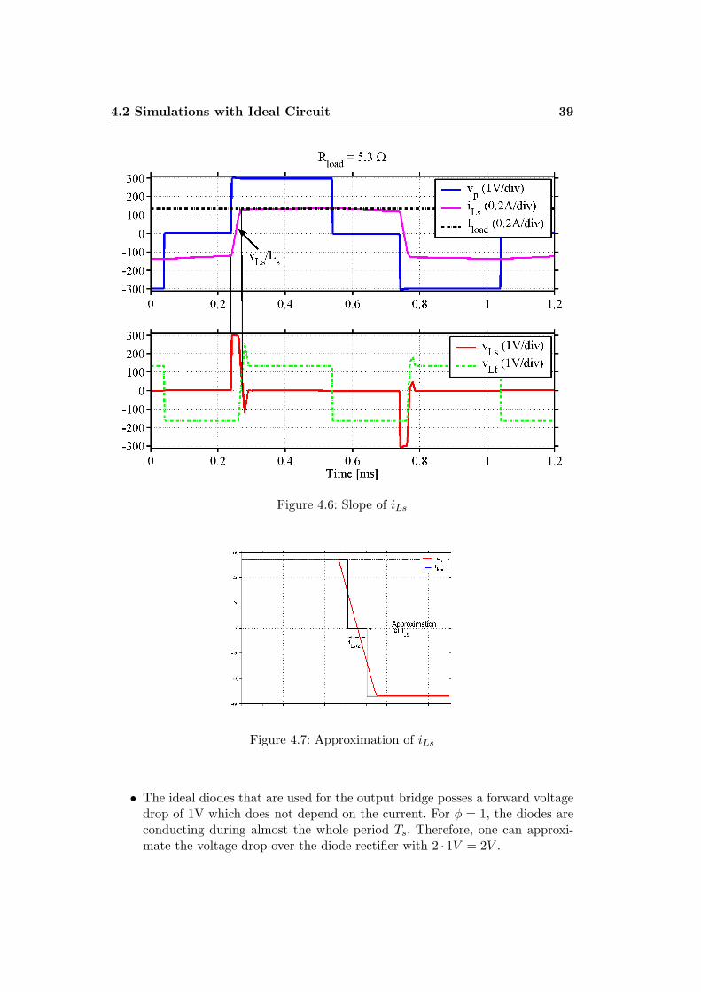
4.2 Simulations with Ideal Circuit 39
Figure 4.6: Slope of iLs
Figure 4.7: Approximation of iLs
• The ideal diodes that are used for the output bridge posses a forward voltagedrop of 1V which does not depend on the current. For φ = 1, the diodes areconducting during almost the whole period Ts. Therefore, one can approxi-mate the voltage drop over the diode rectifier with 2 · 1V = 2V .

40 4 Simulations
• There is also a voltage drop over the filter inductance Lf , but for high φ, theripple of the current through Lf is very low and, hence, the voltage drop overit is negligible.
If one adds up all the voltage drops that are listed above, one gets an overalldifference of 5.1V for the input voltage to the output voltage. In the simulation,the output voltage was 5.4 lower than the input voltage. This small difference canbe explained by the voltage drop over the output filter (which was not quantifiedabove) and the voltage drop over the diodes that are antiparallel to the switches.
4.3 Simulations with Non-Ideal Circuit 41
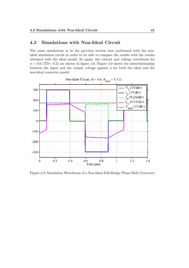
4.3 Simulations with Non-Ideal Circuit
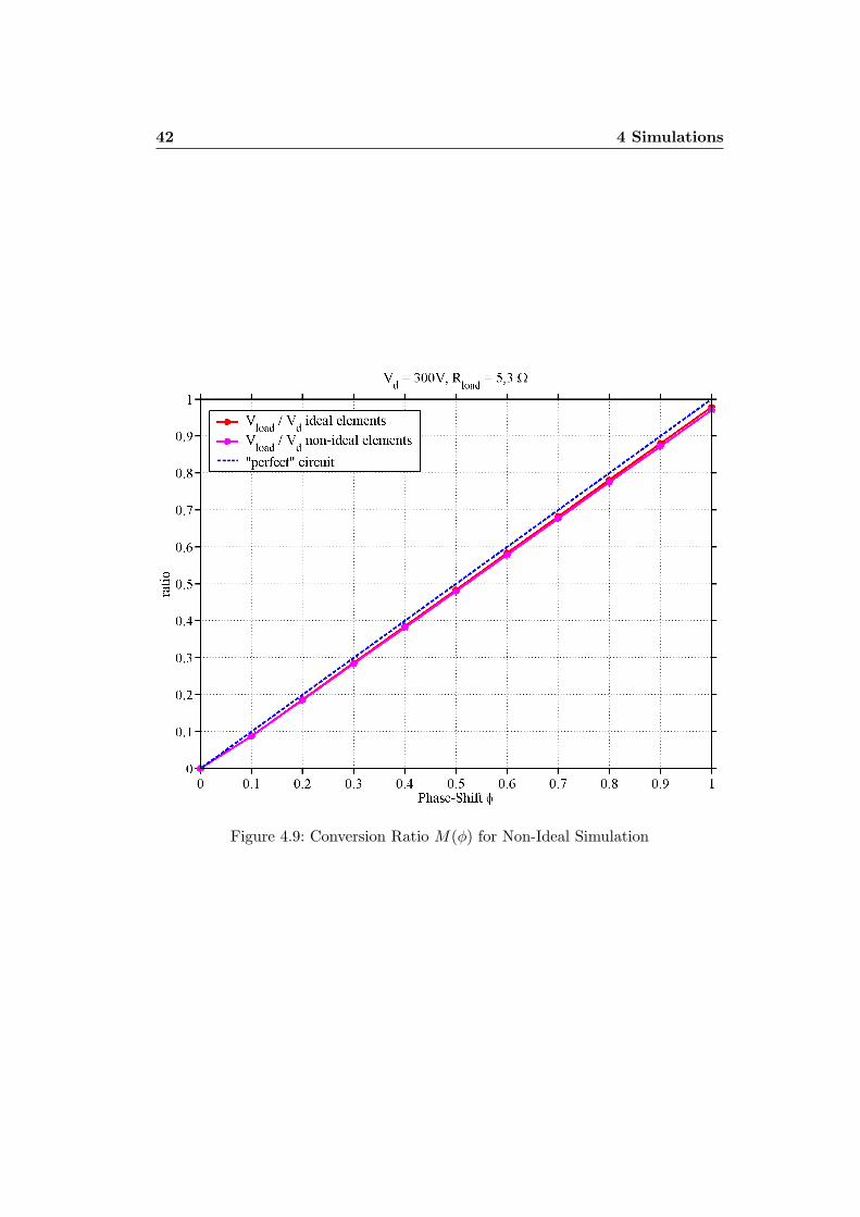
The same simulations as in the previous section were performed with the non-ideal simulation circuit in order to be able to compare the results with the resultsobtained with the ideal model. So again, the current and voltage waveforms forφ = 0.6 (TD= 0.2) are shown in figure 4.8. Figure 4.9 shows the interrelationshipbetween the input and the output voltage against φ for both the ideal and thenon-ideal converter model.
Figure 4.8: Simulation Waveforms of a Non-Ideal Full-Bridge Phase-Shift Converter
42 4 Simulations
Figure 4.9: Conversion Ratio M(φ) for Non-Ideal Simulation
4.3 Simulations with Non-Ideal Circuit 43
4.3.1 Interpretation of the Non-Ideal-Simulation Results
The same phenomena that could be noted in 4.2.1 can also be seen in the simula-tions that were performed with the non-ideal simulation circuit. Additionally, thefollowing facts can be noted:
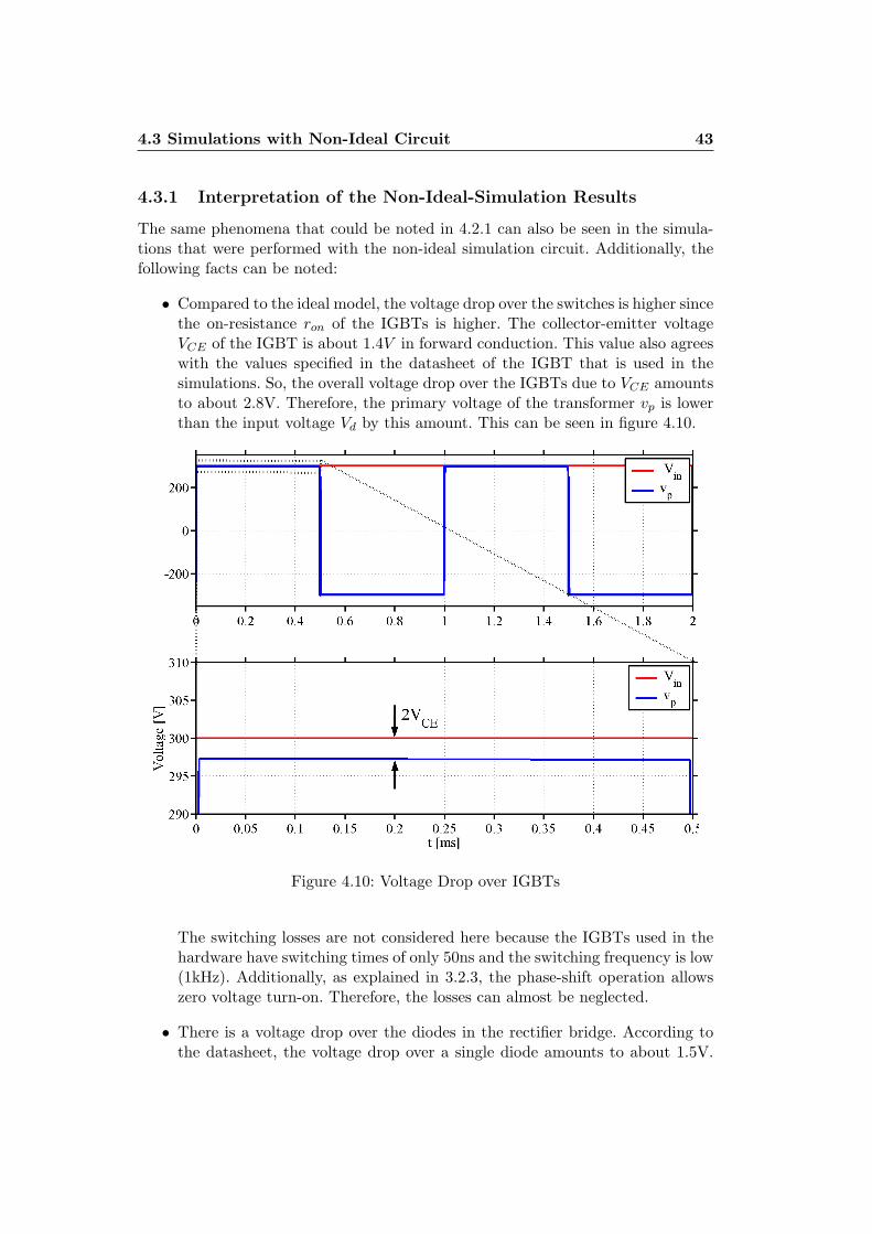
• Compared to the ideal model, the voltage drop over the switches is higher sincethe on-resistance ron of the IGBTs is higher. The collector-emitter voltageVCE of the IGBT is about 1.4V in forward conduction. This value also agreeswith the values specified in the datasheet of the IGBT that is used in thesimulations. So, the overall voltage drop over the IGBTs due to VCE amountsto about 2.8V. Therefore, the primary voltage of the transformer vp is lowerthan the input voltage Vd by this amount. This can be seen in figure 4.10.
Figure 4.10: Voltage Drop over IGBTs
The switching losses are not considered here because the IGBTs used in thehardware have switching times of only 50ns and the switching frequency is low(1kHz). Additionally, as explained in 3.2.3, the phase-shift operation allowszero voltage turn-on. Therefore, the losses can almost be neglected.
• There is a voltage drop over the diodes in the rectifier bridge. According tothe datasheet, the voltage drop over a single diode amounts to about 1.5V.
44 4 Simulations
In the simulations, this value was confirmed. So the overall voltage drop ofthe rectifier input voltage compared to the output voltage amounts to about3.0V.
If one adds up the voltage drops that are calculated above and adds the influ-ences that were already demonstrated for the ideal simulation circuit, one gets anexpected output voltage of 291.2V at full power transfer, i.e. φ = 1. This voltagewas confirmed in the simulations.
4.4 General Comments and Explanations
In this section some general comments and explanations concerning the influenceof certain parts of the phase-shift controlled full-bridge converter are given. Theshown waveforms are all obtained with non-ideal simulations.
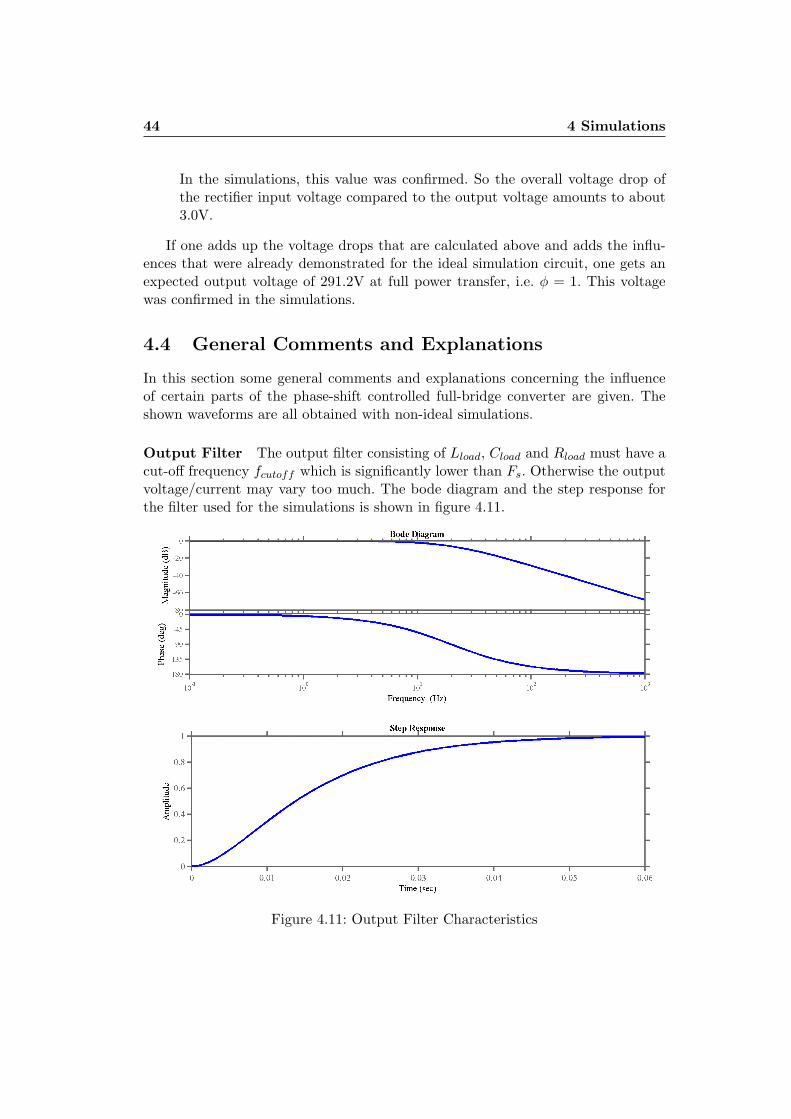
Output Filter The output filter consisting of Lload, Cload and Rload must have acut-off frequency fcutoff which is significantly lower than Fs. Otherwise the outputvoltage/current may vary too much. The bode diagram and the step response forthe filter used for the simulations is shown in figure 4.11.
Figure 4.11: Output Filter Characteristics
4.4 General Comments and Explanations 45
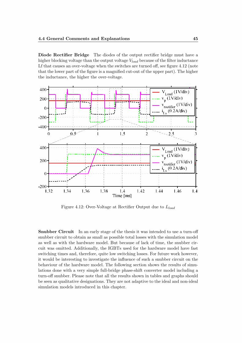
Diode Rectifier Bridge The diodes of the output rectifier bridge must have ahigher blocking voltage than the output voltage Vload because of the filter inductanceLf that causes an over-voltage when the switches are turned off, see figure 4.12 (notethat the lower part of the figure is a magnified cut-out of the upper part). The higherthe inductance, the higher the over-voltage.
Figure 4.12: Over-Voltage at Rectifier Output due to Lload
Snubber Circuit In an early stage of the thesis it was intended to use a turn-offsnubber circuit to obtain as small as possible total losses with the simulation modelas well as with the hardware model. But because of lack of time, the snubber cir-cuit was omitted. Additionally, the IGBTs used for the hardware model have fastswitching times and, therefore, quite low switching losses. For future work however,it would be interesting to investigate the influence of such a snubber circuit on thebehaviour of the hardware model. The following section shows the results of simu-lations done with a very simple full-bridge phase-shift converter model including aturn-off snubber. Please note that all the results shown in tables and graphs shouldbe seen as qualitative designations. They are not adaptive to the ideal and non-idealsimulation models introduced in this chapter.
46 4 Simulations
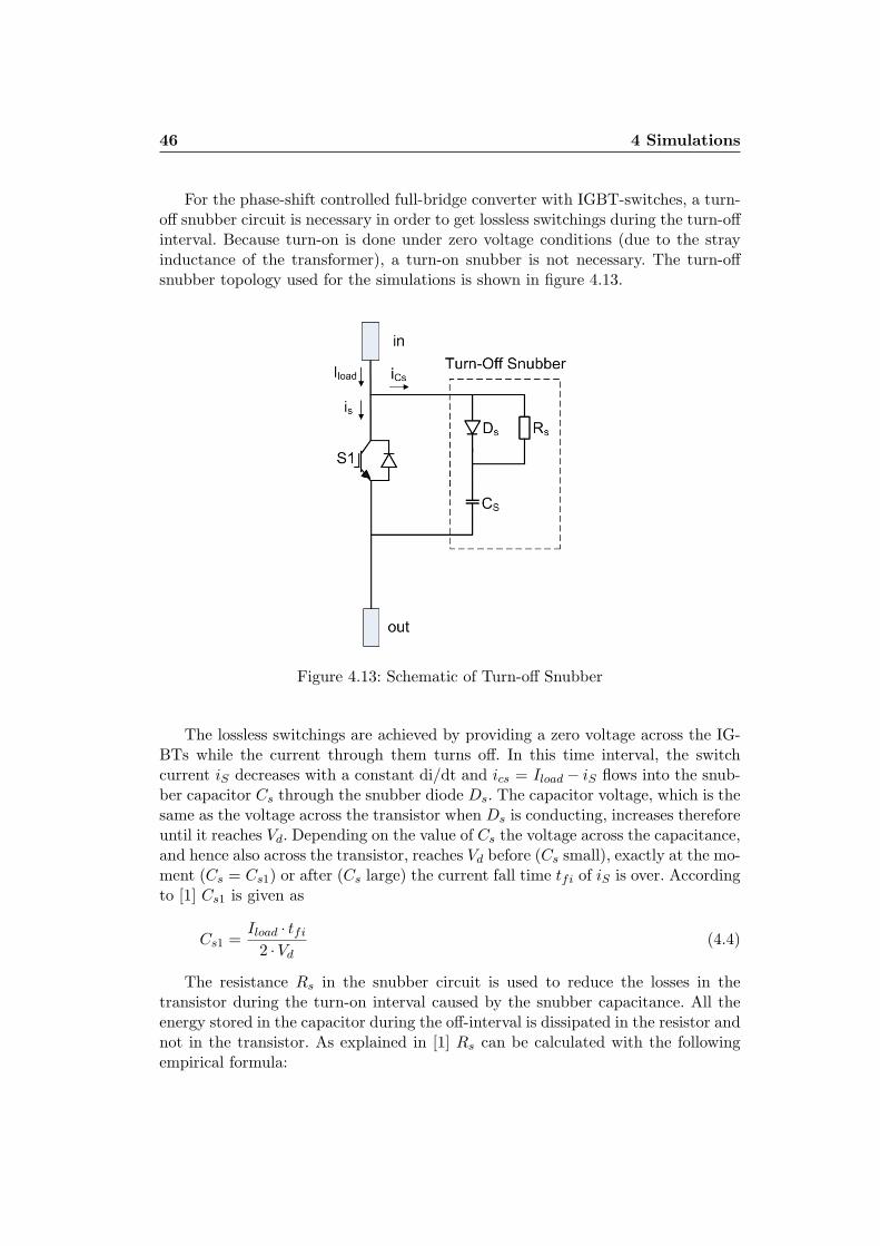
For the phase-shift controlled full-bridge converter with IGBT-switches, a turn-off snubber circuit is necessary in order to get lossless switchings during the turn-offinterval. Because turn-on is done under zero voltage conditions (due to the strayinductance of the transformer), a turn-on snubber is not necessary. The turn-offsnubber topology used for the simulations is shown in figure 4.13.
Figure 4.13: Schematic of Turn-off Snubber
The lossless switchings are achieved by providing a zero voltage across the IG-BTs while the current through them turns off. In this time interval, the switchcurrent iS decreases with a constant di/dt and ics = Iload − iS flows into the snub-ber capacitor Cs through the snubber diode Ds. The capacitor voltage, which is thesame as the voltage across the transistor when Ds is conducting, increases thereforeuntil it reaches Vd. Depending on the value of Cs the voltage across the capacitance,and hence also across the transistor, reaches Vd before (Cs small), exactly at the mo-ment (Cs = Cs1) or after (Cs large) the current fall time tfi of iS is over. Accordingto [1] Cs1 is given as
Cs1 =Iload · tfi
2 ·Vd(4.4)
The resistance Rs in the snubber circuit is used to reduce the losses in thetransistor during the turn-on interval caused by the snubber capacitance. All theenergy stored in the capacitor during the off-interval is dissipated in the resistor andnot in the transistor. As explained in [1] Rs can be calculated with the followingempirical formula:

4.4 General Comments and Explanations 47
Rs =0.2 · Iload
Vd(4.5)
The values for Cs1 and Rs calculated with these two formulas can be seenin tables 4.2 and 4.3. The current fall time tfi was read out from the obtainedsimulation-waveforms.
Table 4.2: Calculation of Cs1 with Equation 4.4
Iload tfi Vd Cs1
48A 2.2us 300V 176nF
Table 4.3: Calculation of Rs with Equation 4.5
Iload Vd Rs
48A 300V 32Ω
The above-mentioned values for the snubber capacitance Cs and the snubberresistance Rs are only a first approximation, particulary the one for Cs. The ap-propriate values have to be found in experiments. Thereby, focus should be laid onminimizing the transistor losses as well as the the sum of transistor and snubberresistance losses.
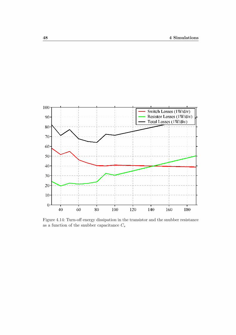
Thus, the converter model was simulated with different snubber configurations.The losses in the transistor and the resistor were simulated, recorded and finallyplotted against the value of Cs. As explained in [1] there should be a minimum ofthe total energy dissipation in the circuit for approximately Cs = 0.5 ·Cs1. As canbe seen in figure 4.14, the results from the simulations confirm this.
Thus, it appears that a turn-off snubber really helps decreasing the losses in afull-bridge phase-shift converter. Further investigations on the basis of the non-idealrefined simulation circuits introduced in chapter 8 should be done to determine aproper snubber configuration.
48 4 Simulations
Figure 4.14: Turn-off energy dissipation in the transistor and the snubber resistanceas a function of the snubber capacitance Cs

Chapter 5
Lab Setup
For the measurements in the laboratory, a 15kW model of the phase-shift con-trolled full-bridge converter was built. This chapter presents a complete list of thecomponents used in the setup that was constructed. Detailed information on theutilisation of these parts and their proper function in the entire system can be foundin the next chapter as well as the appropriate data sheets on the CD enclosed withthis report. Refer to appendix A for all calculations and schematics.
5.1 Entire System
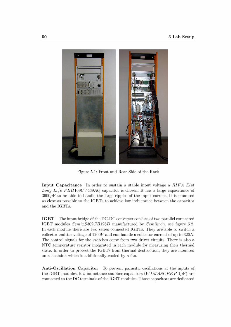
All parts necessary for the DC-DC converter are placed in a rack if it is physicallypossible. Figure 5.1 shows the front and the rear side of this rack. The upper partof it contains the auxiliary control and measuring devices. In the lower part, i.e. onthe aluminium plate, the power components and the primary measuring and controldevices are mounted. The computer in front of the rack is used for controlling theconverter and recording the measured data.
5.2 Components
The converter components can mainly be divided into two classes: the core com-ponents that carry the power and the auxiliary components. This section lists allcomponents used for the lab setup, shows the functions provided by them and ex-plains what they are used for. It does not give detailed specifications about theinterconnections between the single parts and how they realise their role during theoperation. That is explained in the following chapters.
5.2.1 DC-DC Converter Power Components
Voltage Source For the main converter power supply, which should be able toprovide 300V/50A, an external stationary DC generator is used.
50 5 Lab Setup
Figure 5.1: Front and Rear Side of the Rack
Input Capacitance In order to sustain a stable input voltage a RIFA ElytLong Life PEH169UV 439AQ capacitor is chosen. It has a large capacitance of3900µF to be able to handle the large ripples of the input current. It is mountedas close as possible to the IGBTs to achieve low inductance between the capacitorand the IGBTs.
IGBT The input bridge of the DC-DC converter consists of two parallel connectedIGBT modules SemixS302GB128D manufactured by Semikron, see figure 5.2.In each module there are two series connected IGBTs. They are able to switch acollector-emitter voltage of 1200V and can handle a collector current of up to 320A.The control signals for the switches come from two driver circuits. There is also aNTC temperature resistor integrated in each module for measuring their thermalstate. In order to protect the IGBTs from thermal destruction, they are mountedon a heatsink which is additionally cooled by a fan.
Anti-Oscillation Capacitor To prevent parasitic oscillations at the inputs ofthe IGBT modules, low inductance snubber capacitors (WIMASCFKP 1µF) areconnected to the DC terminals of the IGBT modules. Those capacitors are dedicated

5.2 Components 51
Figure 5.2: The SemixS302GB128D IGBT Module
for switching applications and can handle very high voltage peaks.
Stray Inductor In a first step, the transformer was replaced by a 30µH induc-tor that represents the stray inductance, see picture 5.3. Four iron powder toroid(T400A-26) with five turn windings were used for this purpose. This was done be-cause of an unexpected large delay in delivery of the transformer. Since the exactvalue of the later used transformer’s stray inductance was not known, the 30µHwere just a first estimated value.
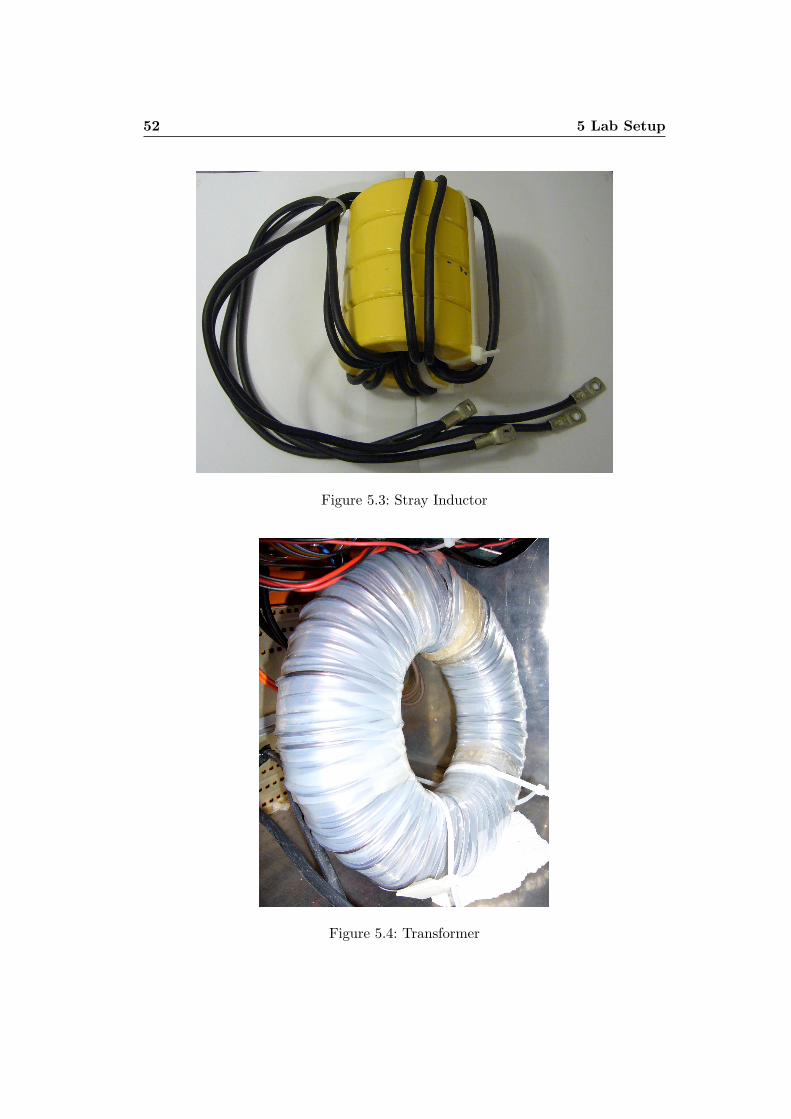
Transformer After doing the measurements with only the stray inductor, acustom-made 1:1 transformer was inserted, see figure 5.4. It has a stray inductanceof 10µH and a main inductance of 14mH. Its core material is iron based magneticalloy 2605SA1 from the manufacturer Metglas. The corresponding data sheet canbe found on the CD or on www.metglas.com. The transformer is also force-cooledby the fan.
Full-Bridge Diode Rectifier The output full-bridge rectifier is made of fourdual high voltage rectifiers (SGS − ThomsonMicroelectronics BY T230PIV −1000). Each of them contains two diodes in parallel which are able to conduct anaverage current of 30A and to block a peak reverse voltage of 1000V. They aremounted on a second heatsink that is also force-cooled by a fan.
52 5 Lab Setup
Figure 5.3: Stray Inductor
Figure 5.4: Transformer
5.2 Components 53
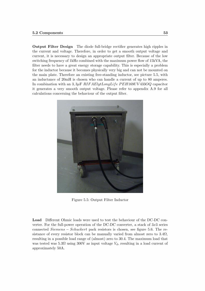
Output Filter Design The diode full-bridge rectifier generates high ripples inthe current and voltage. Therefore, in order to get a smooth output voltage andcurrent, it is necessary to design an appropriate output filter. Because of the lowswitching frequency of 1kHz combined with the maximum power flow of 15kVA, thefilter needs to have a great energy storage capability. This is especially a problemfor the inductor because it becomes physically very big and can not be mounted onthe main plate. Therefore an existing free-standing inductor, see picture 5.5, withan inductance of 20mH is chosen who can handle a current of up to 80 amperes.In combination with an 3, 3µF RIFAElytLongLife PEH169UV 433OQ capacitorit generates a very smooth output voltage. Please refer to appendix A.9 for allcalculations concerning the behaviour of the output filter.
Figure 5.5: Output Filter Inductor
Load Different Ohmic loads were used to test the behaviour of the DC-DC con-verter. For the full-power operation of the DC-DC converter, a stack of 3x3 seriesconnected Siemens − Schuckert pack resistors is chosen, see figure 5.6. The re-sistance of every resistor block can be manually varied from almost zero to 3.4Ω,resulting in a possible load range of (almost) zero to 30.4. The maximum load thatwas tested was 5.3Ω using 300V as input voltage Vd, resulting in a load current ofapproximately 50A.

54 5 Lab Setup
Figure 5.6: Load Resistances
5.2.2 Auxiliary Components
Besides all the power components used to build the actual DC-DC converter, amultiplicity of so-called auxiliary components are needed. They help for examplecontrolling the system, provide signal transmission paths, support cooling the con-verter parts during operation, measure voltage or current and supply the entiresystem with sufficient power.
PC with Simulink The operator of the DC-DC converter should be able tochange settings in realtime and to view the measured data. Hence, a personalcomputer is used. This PC has a built-in dSPACE card with which the wholetransfer of output (drive) and input (measurement) signals is done. Furthermore,the mathematical models of the driving and control circuits are implemented usingSimulink/MATLAB.
dSPACE For some measurements as well as for the control, a dSPACEDS1103controller board is used. This board provides among other things 16+4 A/D input
5.2 Components 55
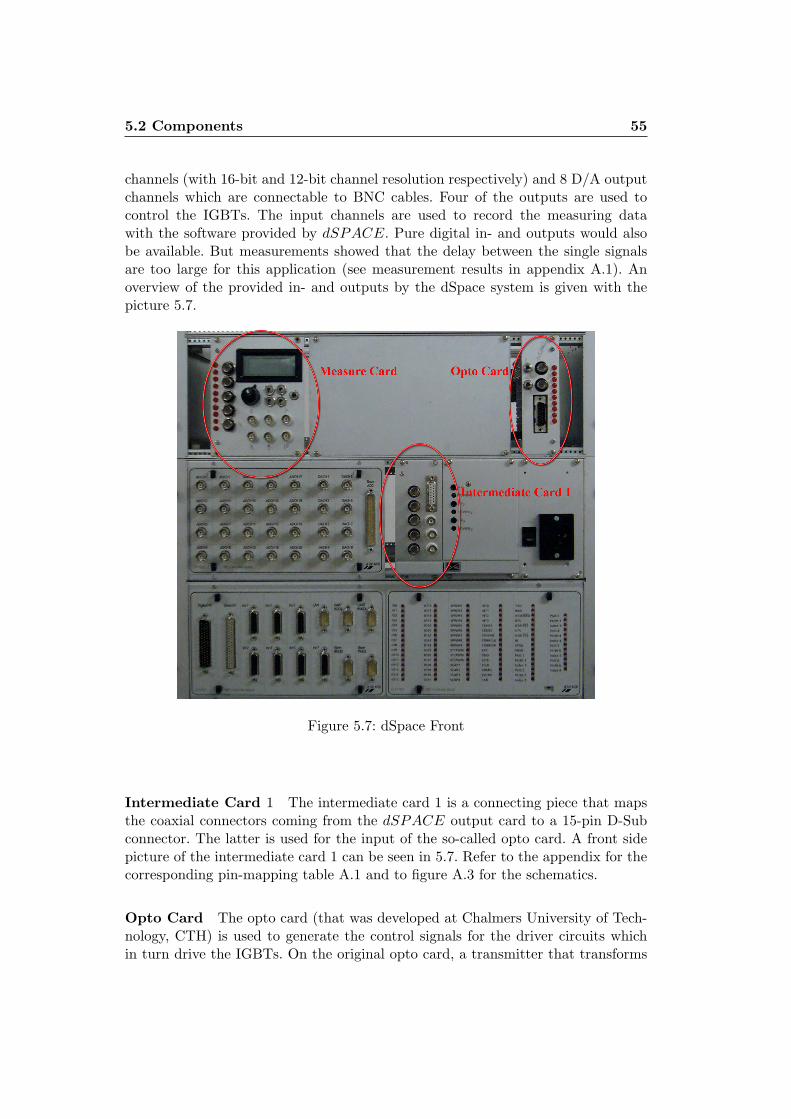
channels (with 16-bit and 12-bit channel resolution respectively) and 8 D/A outputchannels which are connectable to BNC cables. Four of the outputs are used tocontrol the IGBTs. The input channels are used to record the measuring datawith the software provided by dSPACE. Pure digital in- and outputs would alsobe available. But measurements showed that the delay between the single signalsare too large for this application (see measurement results in appendix A.1). Anoverview of the provided in- and outputs by the dSpace system is given with thepicture 5.7.
Figure 5.7: dSpace Front
Intermediate Card 1 The intermediate card 1 is a connecting piece that mapsthe coaxial connectors coming from the dSPACE output card to a 15-pin D-Subconnector. The latter is used for the input of the so-called opto card. A front sidepicture of the intermediate card 1 can be seen in 5.7. Refer to the appendix for thecorresponding pin-mapping table A.1 and to figure A.3 for the schematics.
Opto Card The opto card (that was developed at Chalmers University of Tech-nology, CTH) is used to generate the control signals for the driver circuits whichin turn drive the IGBTs. On the original opto card, a transmitter that transforms
56 5 Lab Setup
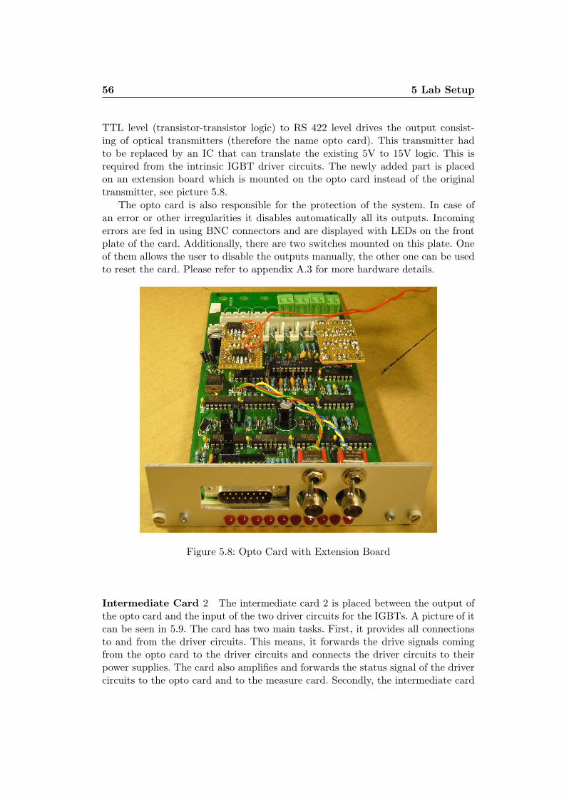
TTL level (transistor-transistor logic) to RS 422 level drives the output consist-ing of optical transmitters (therefore the name opto card). This transmitter hadto be replaced by an IC that can translate the existing 5V to 15V logic. This isrequired from the intrinsic IGBT driver circuits. The newly added part is placedon an extension board which is mounted on the opto card instead of the originaltransmitter, see picture 5.8.
The opto card is also responsible for the protection of the system. In case ofan error or other irregularities it disables automatically all its outputs. Incomingerrors are fed in using BNC connectors and are displayed with LEDs on the frontplate of the card. Additionally, there are two switches mounted on this plate. Oneof them allows the user to disable the outputs manually, the other one can be usedto reset the card. Please refer to appendix A.3 for more hardware details.
Figure 5.8: Opto Card with Extension Board
Intermediate Card 2 The intermediate card 2 is placed between the output ofthe opto card and the input of the two driver circuits for the IGBTs. A picture of itcan be seen in 5.9. The card has two main tasks. First, it provides all connectionsto and from the driver circuits. This means, it forwards the drive signals comingfrom the opto card to the driver circuits and connects the driver circuits to theirpower supplies. The card also amplifies and forwards the status signal of the drivercircuits to the opto card and to the measure card. Secondly, the intermediate card
5.2 Components 57
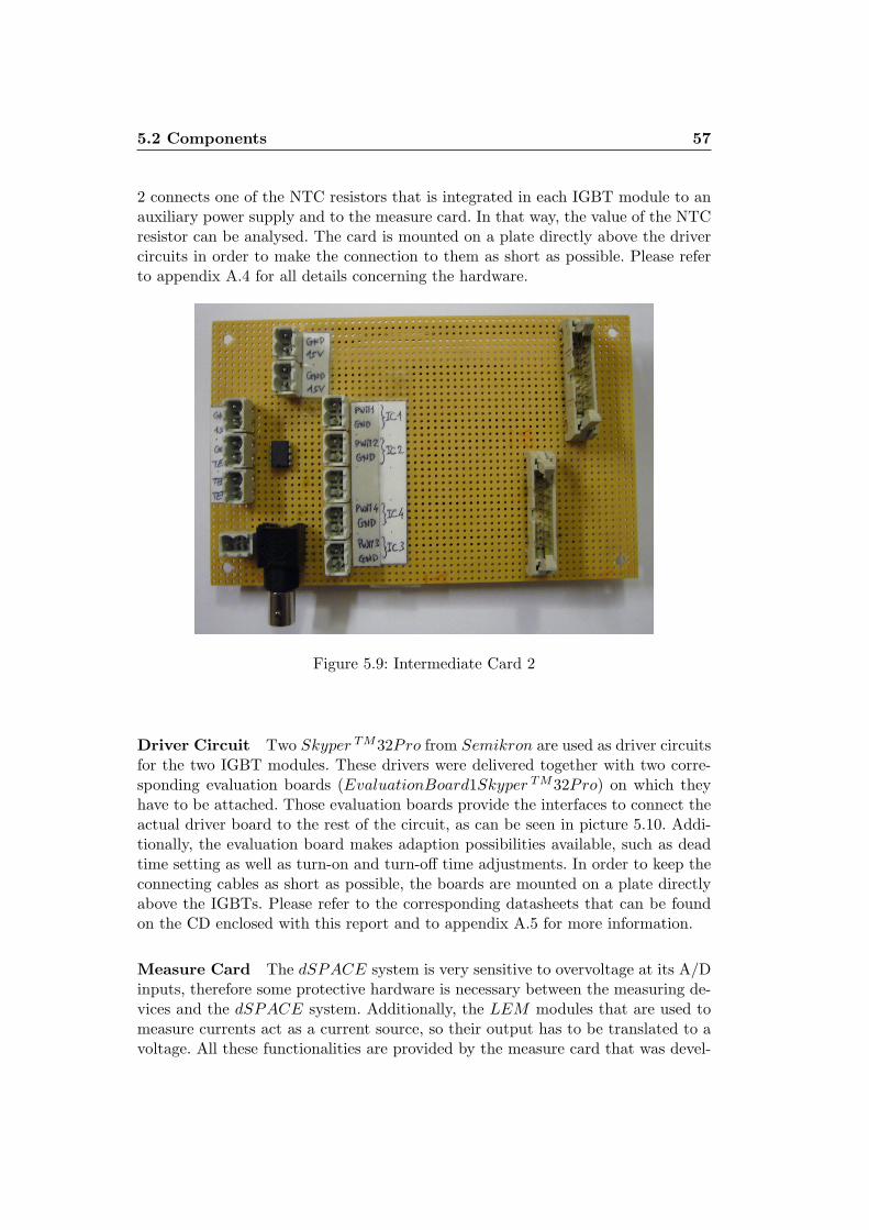
2 connects one of the NTC resistors that is integrated in each IGBT module to anauxiliary power supply and to the measure card. In that way, the value of the NTCresistor can be analysed. The card is mounted on a plate directly above the drivercircuits in order to make the connection to them as short as possible. Please referto appendix A.4 for all details concerning the hardware.
Figure 5.9: Intermediate Card 2
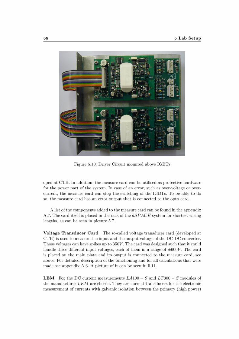
Driver Circuit Two Skyper TM32Pro from Semikron are used as driver circuitsfor the two IGBT modules. These drivers were delivered together with two corre-sponding evaluation boards (EvaluationBoard1Skyper TM32Pro) on which theyhave to be attached. Those evaluation boards provide the interfaces to connect theactual driver board to the rest of the circuit, as can be seen in picture 5.10. Addi-tionally, the evaluation board makes adaption possibilities available, such as deadtime setting as well as turn-on and turn-off time adjustments. In order to keep theconnecting cables as short as possible, the boards are mounted on a plate directlyabove the IGBTs. Please refer to the corresponding datasheets that can be foundon the CD enclosed with this report and to appendix A.5 for more information.
Measure Card The dSPACE system is very sensitive to overvoltage at its A/Dinputs, therefore some protective hardware is necessary between the measuring de-vices and the dSPACE system. Additionally, the LEM modules that are used tomeasure currents act as a current source, so their output has to be translated to avoltage. All these functionalities are provided by the measure card that was devel-
58 5 Lab Setup
Figure 5.10: Driver Circuit mounted above IGBTs
oped at CTH. In addition, the measure card can be utilised as protective hardwarefor the power part of the system. In case of an error, such as over-voltage or over-current, the measure card can stop the switching of the IGBTs. To be able to doso, the measure card has an error output that is connected to the opto card.
A list of the components added to the measure card can be found in the appendixA.7. The card itself is placed in the rack of the dSPACE system for shortest wiringlengths, as can be seen in picture 5.7.
Voltage Transducer Card The so-called voltage transducer card (developed atCTH) is used to measure the input and the output voltage of the DC-DC converter.Those voltages can have spikes up to 350V . The card was designed such that it couldhandle three different input voltages, each of them in a range of ±600V . The cardis placed on the main plate and its output is connected to the measure card, seeabove. For detailed description of the functioning and for all calculations that weremade see appendix A.6. A picture of it can be seen in 5.11.
LEM For the DC current measurements LA100 − S and LT300 − S modules ofthe manufacturer LEM are chosen. They are current transducers for the electronicmeasurement of currents with galvanic isolation between the primary (high power)

5.2 Components 59
Figure 5.11: Voltage Transducer Card
and the secondary (electronic) circuits. They act as a current source. This meansthat their output is a current that is proportional to the current that is measuredwith a ratio of 1 : 2000. Two LA100−S and one LT300−S are placed on differentspots on the converter. The output signal (i.e. the current) is sent to the measurecard.
Heatsink for IGBTs To keep the junction temperature of the IGBTs duringoperation below the given thermal boundary of 125 C, a heatsink is used for cooling.The P16/300 from Semikron is the heatsink recommended from the manufacturerfor this application and seems somewhat oversized, so it was built in without anyfurther calculations.
Heatsink for Rectifier Bridge Due to conduction and switching losses thefour diodes used for the output rectifier bridge can get very hot during operation.In order to protect them against thermal destruction, a heatsink is used for cooling.This heatsink is mounted in a row with the heatsink for the IGBTs and with the fanwhich increases the cooling effect. In order to select the right size of the heatsinksome calculations had to be done, see appendix A.8. As a result of those calculations,the KS216− 100E from Austerlitz − Electronic was chosen.
Fan To obtain a better cooling-effect a fan is connected to the heatsinks for the IG-BTs as well as for the rectifier bridge. This results in a smaller junction-to-ambientthermal resistance of the unit IGBT/heatsink and rectifier/heatsink (approximatelyabout a factor 5). The model that is used is the SKF16A−230−11 from Semikron.
Power Supplies To supply all the parts of the converter as well as the auxiliaryparts with sufficient power, three power supplies are chosen. They provide the sys-
60 5 Lab Setup
tem with +15V , −15V and GND. Two of them can handle maximal current of 1Ashared over all outputs. A Schroff Powerpac PTG and a Hitron HLD12−1.0 arechosen for this purpose. The third power supply is more powerful with a possiblecurrent output of 3.2A (Hitron HLD12−3.4). All of them are built quite compactly,so they can be placed directly into the system close to the other components.
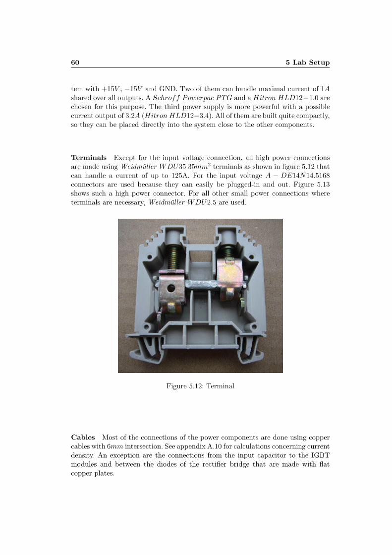
Terminals Except for the input voltage connection, all high power connectionsare made using Weidmuller WDU35 35mm2 terminals as shown in figure 5.12 thatcan handle a current of up to 125A. For the input voltage A − DE14N14.5168connectors are used because they can easily be plugged-in and out. Figure 5.13shows such a high power connector. For all other small power connections whereterminals are necessary, Weidmuller WDU2.5 are used.
Figure 5.12: Terminal
Cables Most of the connections of the power components are done using coppercables with 6mm intersection. See appendix A.10 for calculations concerning currentdensity. An exception are the connections from the input capacitor to the IGBTmodules and between the diodes of the rectifier bridge that are made with flatcopper plates.

5.2 Components 61
Figure 5.13: High Power Connector
5.2.3 Special Measurement Equipment
Digital Oscilloscope A LeCroyLC334A 500MHz digital oscilloscope is used forall measurements of high-frequency signals. If the voltages to be measured are toohigh for the normal inputs, LeCroy AP032 differential probes are used that canhandle voltages up to ±1400V. For all non-DC current measurements, LeCroyAP011 current probes with a bandwidth of 120kHz are used. They can handlecurrents up to 150A.
Power Meter The Fluke 39 Power Meter is used for power analysis. It com-bines the use of a digital multimeter, the visual feedback of an oscilloscope and aharmonics analyzer in a single instrument.
Infrared Temperature Gun The Raytek RayngerST60ProP lus is an infrarednon-contact thermometer with a temperature range of −32 to 600C. It is used forthermal measurements on the two heatsinks and the IGBT-modules.


Chapter 6
The Complete System
This chapter gives an overview of the elaborated concepts used to operate the DC-DC converter that was built in hardware. It explains the power supply concept, thecontrol setup and the measurement setup. It also shows the signal flow and how allparts of the system are interconnected.
6.1 Power Supply Concept
In addition to the main power supply for the input of the DC-DC converter, severalsmaller power supply units are required. The following table 6.1 gives an overviewof the power consumption of all parts needing a power supply. The values in thistable are also given in the corresponding datasheets of the devices.
Table 6.1: Required Power SuppliesPart # Voltage CurrentMain Input 1 300 ≤ 50AMeasure Card 1 ±15V, GND ≈ 30mAOpto Card 1 +15V, GND ≈ 30mAVoltage Transducer Card 1 ±15V, GND ≈ 5mALEM 3 ±15V 22mA + max 100mA outputDriver Circuit 2 +15V, GND 1A peakFan 1 230V, N, GND max 600mATemperature Sensor 1 15V < 15mA
In order to create a clearly designed system, the power supply setup is splitinto two sections, an upper and a lower section. This method supports an easydisconnecting of the DC-DC converter from the rest of the system. The follow-ing paragraphs give a detailed description of each section and figure 6.1 shows aschematic overview of the whole arrangement.
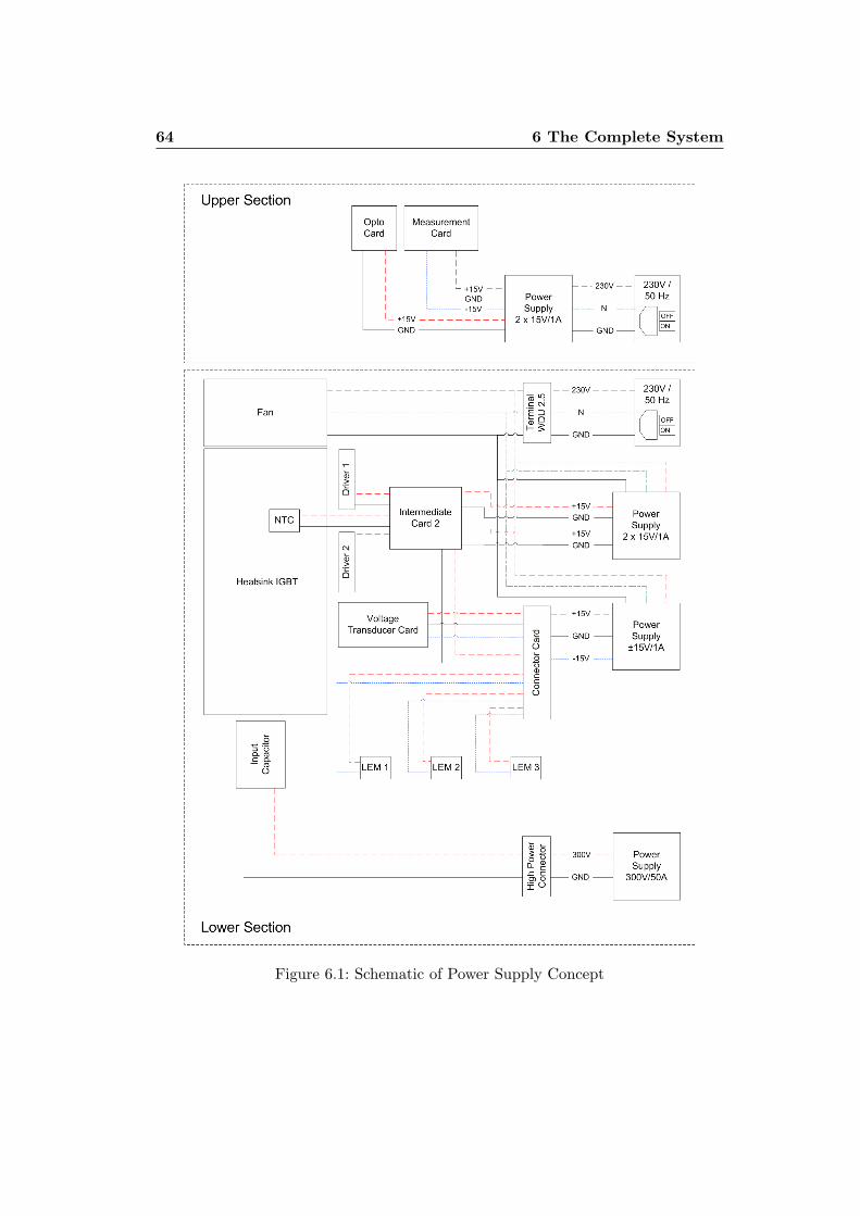
64 6 The Complete System
Figure 6.1: Schematic of Power Supply Concept

6.1 Power Supply Concept 65
Upper Section The upper section contains the supply for the two interface cards(opto card and measurement card) between the converter and the control system. Tokeep the connecting cable short, one power supply unit (Schroff Powerpac PTG)is put in the dSPACE rack next to the two cards. Its outputs are connected in sucha way that it can provide the required ±15V/GND instead of twice +15V/GND.The available output current of 1A is sufficient for the two cards. The power supplyunit itself needs a connection to the 230V/50Hz power line. A plug-in connectionwith a series connected turn-on/off switch is also mounted on the rack to switchthe power supply on and off.
Lower Section As can be seen in table 6.1, there are further devices which needa particular voltage to run. All of them are mounted on the main plate around theDC-DC converter power parts. They form the so-called lower section. As in theupper section, the purpose is to achieve a well-organised power supply with shortconnecting cables and the fewest possible power supply units. The access to the230V power line is done with a normal plug-in connection and a turn-on/off switchfor safety reasons. All the power supply units are connected to it over a terminal(WeidmullerWDU2.5).The fan is the only component in the setup which does not need a special DC-voltage. It can be connected directly to the 230V/50Hz net and, therefore, to theabove mentioned terminals.For the little power consumption of the devices voltage transducer card, LEMmodules and the NTC resistor, one small power supply unit is used. It provides±15V/GND at 1A. Its single output is connected to a connector card where thecables for the consumer loads can be plugged in.For the two driver circuits Skyper TM32Pro an own power supply unit is needed.As can be read in the corresponding datasheets, the two cards make high demandson the power source:
• +15V ±4% voltage supply
• Maximum 50ms trise of supply voltage
• Continuous supply voltage rising slope
• Minimum 1A Ipeak
Hence, a power supply unit was chosen that is able to provide at least 2A (infact 3.2A) output current at +15V . Furthermore, some measurements were done todemonstrate that the other required features can be achieved. These can be seen inappendix A.11.
The input voltage for the DC-DC converter itself is not generated with a powersupply unit mounted directly on the main plate. For this large amount of power(300V/50A) an external DC generator is taken as power supply. The power transferoccurs over two high current cables (200A) which are connected to two high powerconnectors on the main plate.
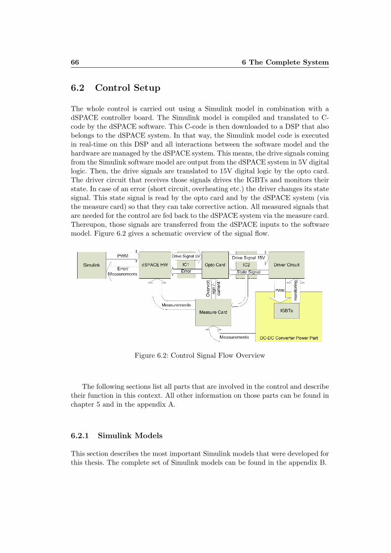
66 6 The Complete System
6.2 Control Setup
The whole control is carried out using a Simulink model in combination with adSPACE controller board. The Simulink model is compiled and translated to C-code by the dSPACE software. This C-code is then downloaded to a DSP that alsobelongs to the dSPACE system. In that way, the Simulink model code is executedin real-time on this DSP and all interactions between the software model and thehardware are managed by the dSPACE system. This means, the drive signals comingfrom the Simulink software model are output from the dSPACE system in 5V digitallogic. Then, the drive signals are translated to 15V digital logic by the opto card.The driver circuit that receives those signals drives the IGBTs and monitors theirstate. In case of an error (short circuit, overheating etc.) the driver changes its statesignal. This state signal is read by the opto card and by the dSPACE system (viathe measure card) so that they can take corrective action. All measured signals thatare needed for the control are fed back to the dSPACE system via the measure card.Thereupon, those signals are transferred from the dSPACE inputs to the softwaremodel. Figure 6.2 gives a schematic overview of the signal flow.
Figure 6.2: Control Signal Flow Overview
The following sections list all parts that are involved in the control and describetheir function in this context. All other information on those parts can be found inchapter 5 and in the appendix A.
6.2.1 Simulink Models
This section describes the most important Simulink models that were developed forthis thesis. The complete set of Simulink models can be found in the appendix B.
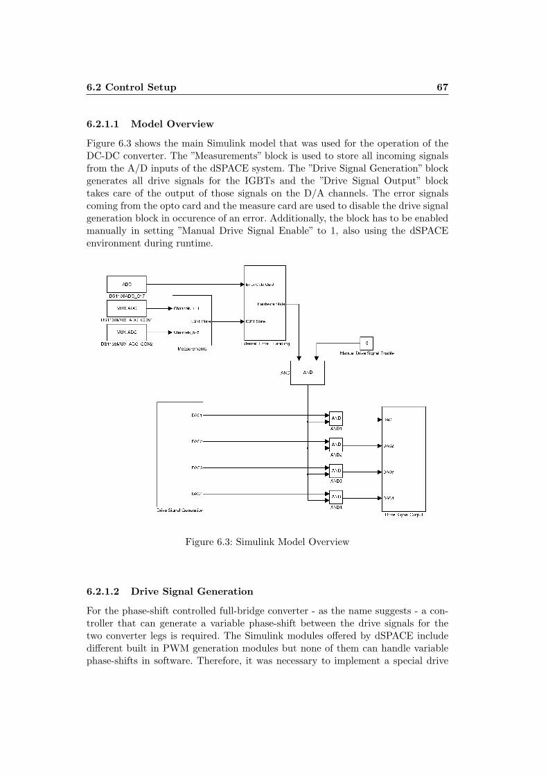
6.2 Control Setup 67
6.2.1.1 Model Overview
Figure 6.3 shows the main Simulink model that was used for the operation of theDC-DC converter. The ”Measurements” block is used to store all incoming signalsfrom the A/D inputs of the dSPACE system. The ”Drive Signal Generation” blockgenerates all drive signals for the IGBTs and the ”Drive Signal Output” blocktakes care of the output of those signals on the D/A channels. The error signalscoming from the opto card and the measure card are used to disable the drive signalgeneration block in occurence of an error. Additionally, the block has to be enabledmanually in setting ”Manual Drive Signal Enable” to 1, also using the dSPACEenvironment during runtime.
Figure 6.3: Simulink Model Overview
6.2.1.2 Drive Signal Generation
For the phase-shift controlled full-bridge converter - as the name suggests - a con-troller that can generate a variable phase-shift between the drive signals for thetwo converter legs is required. The Simulink modules offered by dSPACE includedifferent built in PWM generation modules but none of them can handle variablephase-shifts in software. Therefore, it was necessary to implement a special drive
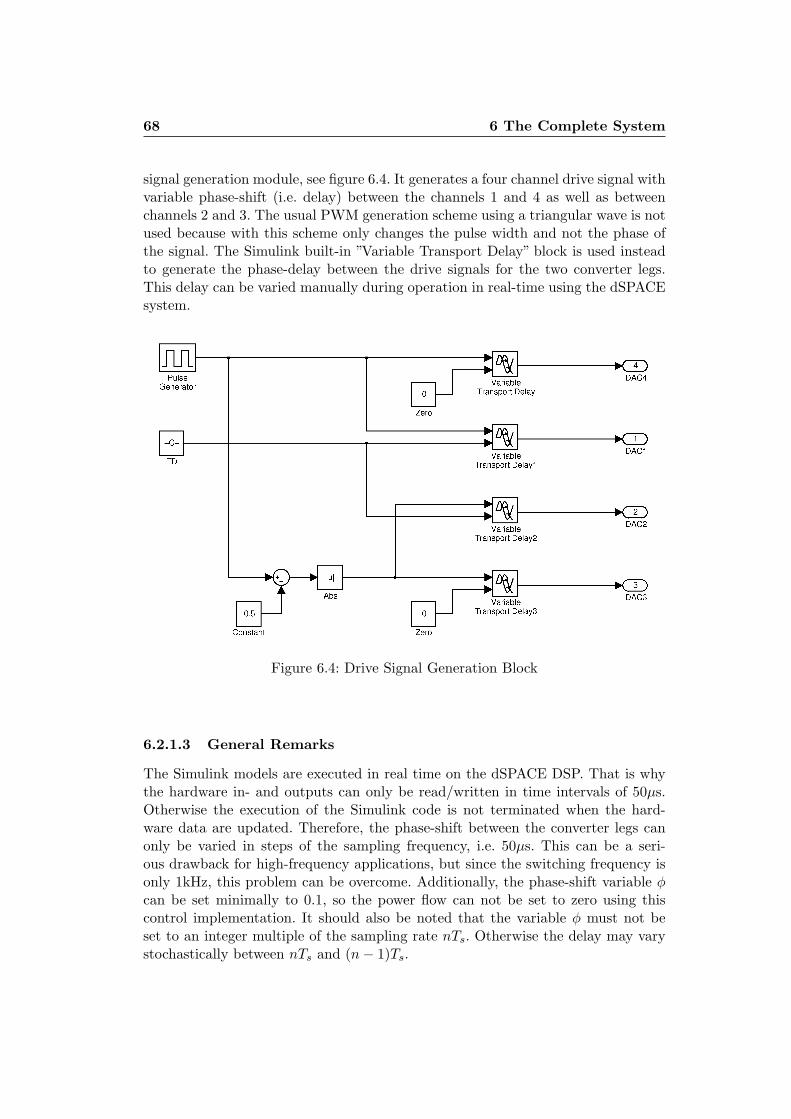
68 6 The Complete System
signal generation module, see figure 6.4. It generates a four channel drive signal withvariable phase-shift (i.e. delay) between the channels 1 and 4 as well as betweenchannels 2 and 3. The usual PWM generation scheme using a triangular wave is notused because with this scheme only changes the pulse width and not the phase ofthe signal. The Simulink built-in ”Variable Transport Delay” block is used insteadto generate the phase-delay between the drive signals for the two converter legs.This delay can be varied manually during operation in real-time using the dSPACEsystem.
Figure 6.4: Drive Signal Generation Block
6.2.1.3 General Remarks
The Simulink models are executed in real time on the dSPACE DSP. That is whythe hardware in- and outputs can only be read/written in time intervals of 50µs.Otherwise the execution of the Simulink code is not terminated when the hard-ware data are updated. Therefore, the phase-shift between the converter legs canonly be varied in steps of the sampling frequency, i.e. 50µs. This can be a seri-ous drawback for high-frequency applications, but since the switching frequency isonly 1kHz, this problem can be overcome. Additionally, the phase-shift variable φcan be set minimally to 0.1, so the power flow can not be set to zero using thiscontrol implementation. It should also be noted that the variable φ must not beset to an integer multiple of the sampling rate nTs. Otherwise the delay may varystochastically between nTs and (n− 1)Ts.
6.2 Control Setup 69
6.2.2 dSPACE
As mentioned before, a dSPACE DS1103 controller board that uses an underlyingSimulink controller model is used to operate the DC-DC converter. The Simulinkcontroller model is compiled and downloaded to a DSP that belongs to the dSPACEsystem. All communication between the software controller model and the hardwareis performed by the dSPACE system. This means, that also the IGBT drive signalsare generated using the dSPACE board. However, the D/A outputs of the dSPACEsystem can not directly be fed to the IGBT driver circuit. The dSPACE systemcan only generate signals in a range of ±10V, but the driver circuit needs 15Vdigital logic. In addition, the dSPACE output could not deliver enough current tothe driver circuit. Therefore, some intermediate hardware is necessary, namely theopto card that is described in the next section 6.2.3.
The software controller model needs also to monitor the state of the DC-DCconverter, therefore all measured signals are fed to the A/D inputs of the dSPACEboard. Those inputs are sensitive to overvoltage so it is necessary to protect themby some hardware. This duty is taken over by the measure card, see section 6.2.7.Please refer to the appendix A.1 for all measurements and tests that were donewith the dSPACE hardware in order to verify its functionality for our purposes.
6.2.3 Opto Card
As mentioned above, the opto card is used to translate the drive signals for theIGBTs from 5V to 15V logic. Its output is fed into the driver circuit. The opto cardhas two error inputs that disable the card when an error signal is present (high orlow logic). One error signal is connected to the IGBT driver circuit using its statussignal (IF CMN nHALT ). This signal changes its status to low whenever an erroris detected. The other error onput is connected to the measure card, that sends anerror signal in case there is an overvoltage/overcurrent detected. Hence, if an erroroccurs at the IGBT driver circuit or elsewhere at the DC-DC converter powerstage, the opto card is immediately switched off. This prevents the destruction ofthe IGBTs or other hardware in case of failure.
6.2.4 Intermediate Card 1
The intermediate card 1 forwards the drive signals received from the dSPACEsystem to the opto card. In the other direction, the card sends the state signal ofthe opto card to the dSPACE system.
6.2.5 Driver Circuit
The driver circuit generates the actual driving signals for the IGBTs. Furthermore,the driver circuit monitors also the state of the IGBTs. Overheating, short-circuitsand other serious failures can be detected. The driver provides a status signal thatis used to switch off the opto card in case of an error to stop generating drive

70 6 The Complete System
signals. The error signal is also fed back to the dSPACE simulation software via themeasure card. Please refer to the appendix A.5 and to the corresponding datasheetsfor a complete list of adjustments and monitoring possibilities that are provided bythe driver circuit.
6.2.6 Intermediate Card 2
The intermediate card 2 forwards the drive signals for the IGBTs from the optocard to the driver circuits. In the opposite direction, it splits up the state signal ofthe IGBT driver circuits and sends them to the opto card as well as to the dSPACEsystem via the measure card. Please refer to section 5.2.2 and to the appendix A.4for all hardware details.
6.2.7 Measure Card
In normal operation, the measure card forwards the down-scaled voltages measuredon the main plate to the dSPACE system without changing them. Additionally, ittranslates the current coming from the LEM modules to a voltage in the rangeof ±2.5V. It also provides four different reference signals that can be changed inorder to set custom voltage/current threshold signals. Every measure signal must beassigned to one of those thresholds and if it exceeds it, an error signal is generated.This error signal is connected to the opto card to stop the drive signals for the IGBTsimmediately. This security function was implemented in hardware deliberately inorder to have shortest possible reaction time in occurrence of an error. The errorsignal is also forwarded to the dSPACE system so that the software is able to learnabout this error. See also appendix A.7 for the complete hardware setup of themeasure card.
6.3 Measurement Setup
As mentioned above, the dSPACE system used to control and monitor the DC-DC converter can only operate with a finite sampling ratio. This is due to thesoftware that needs to be executed in real time on the DSP of the dSPACE board,see also 6.2.1. The sampling rate is about 20kHz. Therefore, the dSPACE systemcan not be used to measure and record the high-frequency signal components thatare generated by the switching of the IGBTs. The output filter inductor eliminatesmost of the high-frequency components of the power flow, so its output current isthe first signal (after the input current and input voltage) that can be monitoredby the dSPACE system. So it is only the low-frequency or the DC componentsthat are measured and recorded using the dSPACE system. Figure 6.5 shows thesignals that can be measured with dSPACE. The schematic signal flow of the abovementioned part of the measurement setup can be seen in figure 6.6.
For all high-frequency signals, a LeCroy digital oscilloscope is used, as mentionedin chapter 5.
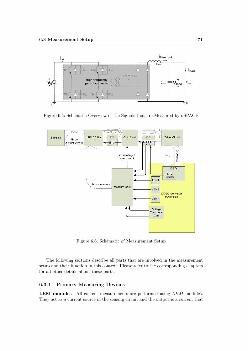
6.3 Measurement Setup 71
Figure 6.5: Schematic Overview of the Signals that are Measured by dSPACE
Figure 6.6: Schematic of Measurement Setup
The following sections describe all parts that are involved in the measurementsetup and their function in this context. Please refer to the corresponding chaptersfor all other details about these parts.
6.3.1 Primary Measuring Devices
LEM modules All current measurements are performed using LEM modules.They act as a current source in the sensing circuit and the output is a current that
72 6 The Complete System
is proportional to the measured one. Therefore, their signals need to be translatedto a voltage so that the dSPACE system is able to register the value. This task isdone on the measure card, where a resistor in series to ground is inserted and thevoltage drop over the resistor is measured, see also section 6.3.2.
The LEM modules were used to measure the input current, the output currentof the filter inductance and the load current. The filter output current is not com-pletely DC, it still has ripples. So the measured signal was only used for monitoringpurposes and not recorded.
Voltage Transducer Card The voltage transducer card measures the input andthe output voltage of the DC-DC converter and forwards the down-scaled signalsto the measure card. All other voltages possess high-frequency components whichcan not be handled by the AD210 isolation amplifier that is used on the voltagetransducer card. Also the dSPACE system can not handle those high-frequencysignals as mentioned before. Please refer to the appendix A.6 for all hardwaredetails of the voltage transducer card.
Temperature Measurement The two IGBT modules have a built-in NTC re-sistor each. One of those NTC resistors is connected to the driver circuit to stopthe IGBTs in case of overheating. The other NTC resistor is used to measure thetemperature for the control and measurement system. This resistor is connectedto a 15V power supply on one end. On the other end, the resistor is connected toground via another resistor that is mounted on the measure card. The voltage dropover this second resistor is fed forward to the dSPACE system and the temperatureof the IGBT can be calculated. Please refer to the datasheet of the IGBT on theCD enclosed with this report for more details concerning the built-in NTC resistor.
6.3.2 Measure Card
The measure card has two main tasks. First, all measurement signals in form ofcurrents need to be translated to voltages. The second task is to stop feeding forwardthe (down-scaled) measured voltages in case they are higher than ±10V in ordernot to destroy the dSPACE A/D inputs (or if they exceed the custom set thresholdlevel, see section 6.2.7). Also the DC-DC converter is stopped in case of this errorby disabling the opto card. Most errors concerning the IGBTs are detected by thedriver circuit first and so the IGBT would stop operating anyway. But in case thereis a failure that can not be detected by the driver circuit, the measure card can stopthe converter. Please refer to appendix A.7 for all hardware details of the measurecard.

6.3 Measurement Setup 73
6.3.3 dSPACE
The dSPACE system has 16 A/D channels with 16-bit resolution and 4 A/D chan-nels with 12 bit resolution. For all measurements, the channels with 16-bit resolutionare used.
The dSPACE software includes tools to monitor and change all model data andparameters (software as well as hardware) during run-time. It also provides a tool torecord data in the comma-separated values (csv) file format that is easily processedby other programs. So all data are recorded using this csv format. Note that allmeasurement data can only be stored at multiple integers of the sampling time. Soas mentioned before, only low-frequency signals are recorded using dSPACE.
6.3.4 Digital Oscilloscope
High-frequency transients are measured and recorded using a LeCroy digital oscil-loscope with a sampling ration of 500MHz. It can be connected to a PC using aRS232 connection. Both graphs and traces can be stored.

Chapter 7
Measurement Results
After the hardware setup that is described in the two previous chapters was built,measurements were carried out. In a first stage, measurements without a trans-former were performed. The transformer was replaced by an inductor that rep-resents its stray inductance. Afterwards, a custom-made 1 : 1 transformer wasinserted. This chapter presents the results obtained with the different setups.
7.1 Measurements without Transformer
As mentioned above, the transformer was replaced by an inductor that representsits stray inductance in the first stage of the measurements. This was done becauseof two main reasons. The first reason is the risk of DC-saturation of the transformerin case the control soft- and hardware do not operate the switches in a perfectlysymmetric way. The second reason are large delays in delivery of the transformer.But since the transformer does not change the voltage level, no large differenceswere expected from the measurements performed with and without the transformer.The following sections present the measurement results gained from the the formersetup.
7.1.1 Overview
In figure 7.1 a general overview of the most important currents and voltages of theconverter is shown. Figure 7.2 shows the interrelationship between the input andthe output voltage against φ. It can be seen that there seem to be large currentdependent losses (i.e. conduction losses) because the line flattens out as φ -andtherefore also the current- increases.
The total input and the total output power were also measured. This was doneusing the input/output current and voltage measured with dSPACE over severalseconds. It was found out, that the losses amount to about 730W at full load, i.e.at ≈ 300V input voltage and ≈ 50A input current.
76 7 Measurement Results
Figure 7.1: Measured Waveforms of the Full-Bridge Phase-Shift Converter withoutTransformer
7.1.2 Detail Analysis
This section analyses the different parts that were involved in the measurements.Especially all possible sources for losses during operation are investigated. Theoverall loss at φ = 1 was calculated to be about 750W, with 14.05kW input powerand 13.3 kW output power.
7.1.2.1 Switches
IGBT conduction losses The voltage drop over an IGBT, i.e. its collector emit-ter voltage VCE , can be seen very well when the current through the IGBT changesdirection. Figure 7.3 illustrates the turn-on of an IGBT (no. 3 in this case) and howthe voltage over the IGBT changes sign at the moment the current iLs crosses zero(the current does not change direction immediately when the switch is turned onbecause of the finite value of the inductance that represents the stray inductance).The datasheet of the IGBTs specifies a typical collector emitter voltage VCE0 of0.9 − 1.1 V. As can be seen in the lower part of figure 7.3 the measurements ver-ify this voltage range. For this plot the input voltage was chosen low to make the

7.1 Measurements without Transformer 77
Figure 7.2: The Input/Output Interrelation against φ)
voltage drop over the IGBTs clearly visible. Therefore, the slope of iLs which isproportional to vp/Ls (i.e. also directly proportional to Vd) is not steep.
The conduction losses of the IGBTs can rather easily be estimated: The averagecurrent through the IGBTs at full power transfer (φ=1) amounts to roughly 50A.For this current, the collector-emitter voltage VCE amounts to about 1.4V accordingto the graph on the datasheet. The current always flows through two IGBTs on itspath. Therefore, the conduction losses of the IGBTs Pcond IGBT can be estimatedusing
Pcond IGBT ≈ 2 · 50A · 1.4V = 140W. (7.1)
Other losses in the IGBTs The loss during turn-on and turn-off can roughlybe estimated using typical data from the manufacturer that can be found on thedatasheet. For 50A switch current and a gate resistance of RG = 15Ω, the energybeing dissipated during each turn-on is specified with about 10.5mJ, the energy lostduring turn-off with about 9.5mJ. Therefore, one can estimate the switching lossesin all four IGBTs with
Pswitching math = Ploss turn−on + Ploss turn−off (7.2)
78 7 Measurement Results
Figure 7.3: Current and Voltage Waveforms during Turn-On of an IGBT
= 10.5mJ ·Fs · 4 + 9.5mJ ·Fs · 4 = 42W + 38W = 80W.
The switching losses of the IGBTs can not be measured directly, since thecurrent through the switch can not be measured. Also the losses in the antiparalleldiodes that are integrated in each IGBT module can not be defined. The overall lossof the IGBTs however can be estimated using thermal measurements. The case-to-sink thermal resistance RΘ,cs of the IGBTs is given in the corresponding datasheetwith 0.045
CW . The temperature difference of the IGBT module to the heatsink was
measured to be 5 C at steady state. For this measurement, the infrared temperaturegun was used1. Using the above mentioned values, the overall losses in one module(which contains two IGBTs) can be estimated with:
Ploss measured =δT
RΘ,cs=
5 C0.045 C
W
≈ 110W. (7.3)
This means, that the total losses of the two IGBT modules and their antiparalleldiodes amount to ≈ 220W. Together with the conduction loss analysis from above,
1The measured temperature difference of 5 C might be inexact because the temperature guncan produce imprecise results when applied on polished metal surfaces. The heatsink of the IGBTshas such a surface, but when black tape was used to cover the surface, the results got worse.
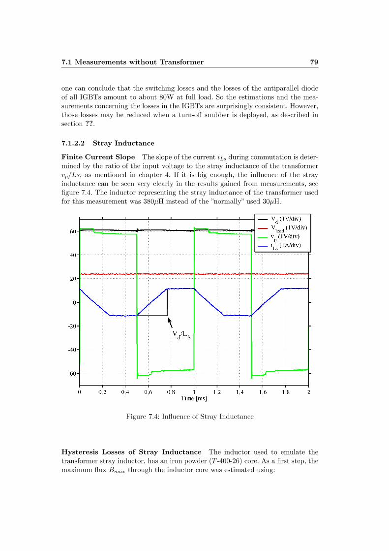
7.1 Measurements without Transformer 79
one can conclude that the switching losses and the losses of the antiparallel diodeof all IGBTs amount to about 80W at full load. So the estimations and the mea-surements concerning the losses in the IGBTs are surprisingly consistent. However,those losses may be reduced when a turn-off snubber is deployed, as described insection ??.
7.1.2.2 Stray Inductance
Finite Current Slope The slope of the current iLs during commutation is deter-mined by the ratio of the input voltage to the stray inductance of the transformervp/Ls, as mentioned in chapter 4. If it is big enough, the influence of the strayinductance can be seen very clearly in the results gained from measurements, seefigure 7.4. The inductor representing the stray inductance of the transformer usedfor this measurement was 380µH instead of the ”normally” used 30µH.
Figure 7.4: Influence of Stray Inductance
Hysteresis Losses of Stray Inductance The inductor used to emulate thetransformer stray inductor, has an iron powder (T -400-26) core. As a first step, themaximum flux Bmax through the inductor core was estimated using:
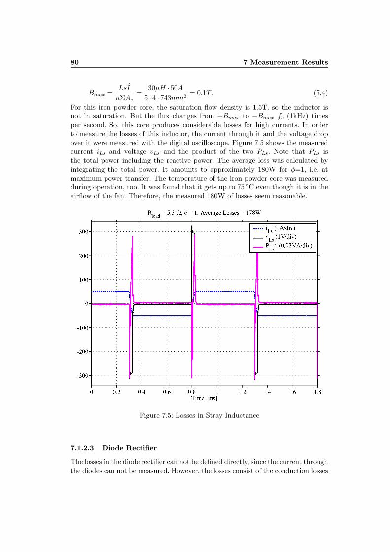
80 7 Measurement Results
Bmax =LsI
nΣAe=
30µH · 50A
5 · 4 · 743mm2= 0.1T. (7.4)
For this iron powder core, the saturation flow density is 1.5T, so the inductor isnot in saturation. But the flux changes from +Bmax to −Bmax fs (1kHz) timesper second. So, this core produces considerable losses for high currents. In orderto measure the losses of this inductor, the current through it and the voltage dropover it were measured with the digital oscilloscope. Figure 7.5 shows the measuredcurrent iLs and voltage vLs and the product of the two PLs. Note that PLs isthe total power including the reactive power. The average loss was calculated byintegrating the total power. It amounts to approximately 180W for φ=1, i.e. atmaximum power transfer. The temperature of the iron powder core was measuredduring operation, too. It was found that it gets up to 75 C even though it is in theairflow of the fan. Therefore, the measured 180W of losses seem reasonable.
Figure 7.5: Losses in Stray Inductance
7.1.2.3 Diode Rectifier
The losses in the diode rectifier can not be defined directly, since the current throughthe diodes can not be measured. However, the losses consist of the conduction losses
7.1 Measurements without Transformer 81
and the switching losses. According to the manufacturer the switching losses canbe neglected for this application, so
PLoss = Pconduction + Pswitching ≈ Pconduction. (7.5)
According to the manufacturers’ instructions of the diodes that are used for therectifier bridge, the losses can be estimated as follows:
Pconduction = 1.47 · IF,(AV ) + 0.01 · I2F,(RMS). (7.6)
The calculation of this loss is done in appendix A.8. The result is an overall lossof the diode output bridge Pconduction of approximately 176W. The sink-to-ambientthermal resistance of the heatsink is RΘ,sa = 0.08
CW . This means that at full load,
i.e. with 50A flowing through the rectifier bridge, the temperature difference of theheatsink to the surrounding area amounts to:
δT = RΘ,saPconduction ≈ 14 C. (7.7)
In reality, a heatsink temperature that was 13 C warmer than the surrounding wasmeasured at steady state. This leads to a total loss of Pconduction ≈ 163W. Thosetwo results match very well.
7.1.2.4 Filter Inductance
The filter inductance Lf was chosen very high (20mH) to get smooth output currentand voltage. Apparently, there are also hysteresis and copper losses in this inductor.Hence, the current through the filter inductor was measured together with thevoltage drop over it. The results can be seen in figure 7.6. The real part of the powerwas again calculated in integrating the overall power through the filter inductor.It amounts to ≈ 110W. This inductor does not get significantly warmer since it isphysically very big, so no thermal measurements were performed.
7.1.3 Conclusions
If one adds up all the losses that were found with detail analysis, then a total loss ofabout 680W results. Compared to the measured difference between the input andthe output power (750W), this is a deviation of only 70W. This difference can beexplained by the limited resolution in time and/or in current/voltage of the mea-suring devices used. Also the temperature gun used for the thermal measurementshas a certain inaccuracy. However, if the input voltage and the output voltage arecompared, this results in a ratio of Vd/Vload = 91.2%. However, if the input powerand the output power are compared, this yields to a ratio of Pin/Pout = 94.7%.A possible explanation for this is that, without transformer, the topology used issimilar to the Buck converter. There, the ratio of the input current to the outputcurrent is inversely proportional to the ratio of the switch on-time to the switch off-time, see section 2.1. Here, the switch off-time is the time during which no voltage
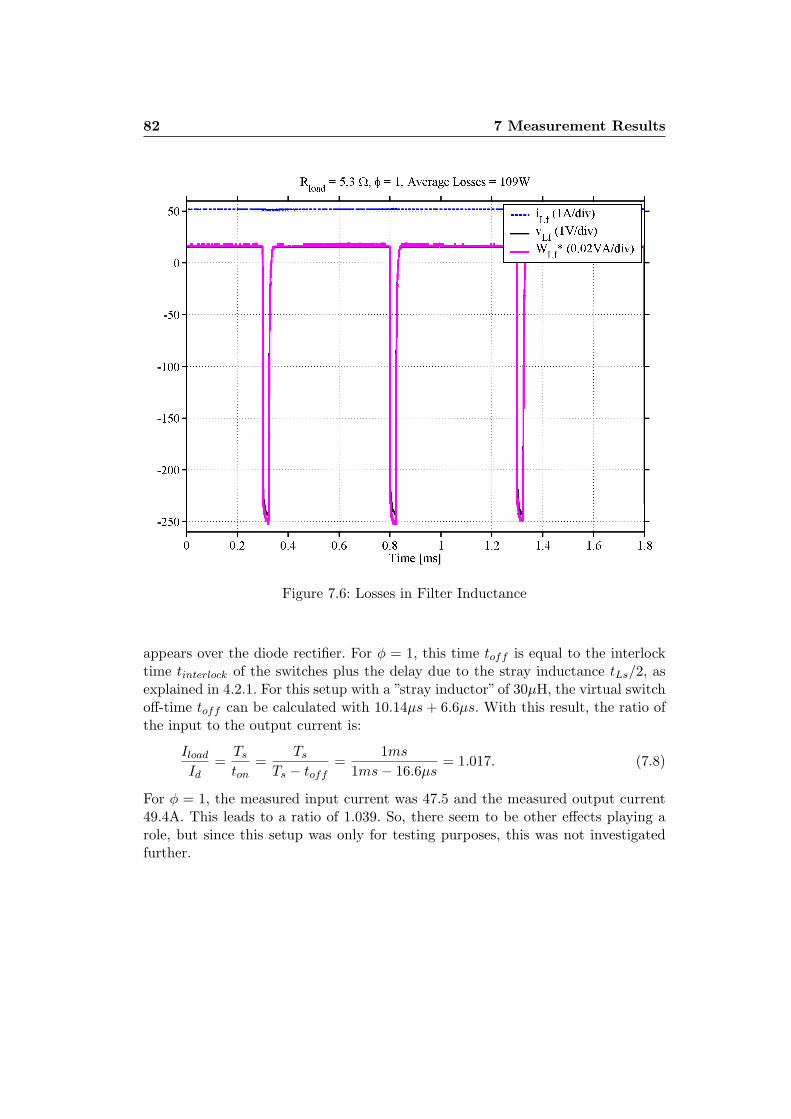
82 7 Measurement Results
Figure 7.6: Losses in Filter Inductance
appears over the diode rectifier. For φ = 1, this time toff is equal to the interlocktime tinterlock of the switches plus the delay due to the stray inductance tLs/2, asexplained in 4.2.1. For this setup with a ”stray inductor”of 30µH, the virtual switchoff-time toff can be calculated with 10.14µs + 6.6µs. With this result, the ratio ofthe input to the output current is:
Iload
Id=
Ts
ton=
Ts
Ts − toff=
1ms
1ms− 16.6µs= 1.017. (7.8)
For φ = 1, the measured input current was 47.5 and the measured output current49.4A. This leads to a ratio of 1.039. So, there seem to be other effects playing arole, but since this setup was only for testing purposes, this was not investigatedfurther.
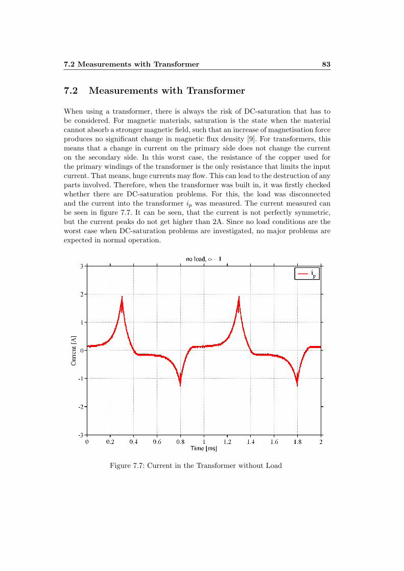
7.2 Measurements with Transformer 83
7.2 Measurements with Transformer
When using a transformer, there is always the risk of DC-saturation that has tobe considered. For magnetic materials, saturation is the state when the materialcannot absorb a stronger magnetic field, such that an increase of magnetisation forceproduces no significant change in magnetic flux density [9]. For transformers, thismeans that a change in current on the primary side does not change the currenton the secondary side. In this worst case, the resistance of the copper used forthe primary windings of the transformer is the only resistance that limits the inputcurrent. That means, huge currents may flow. This can lead to the destruction of anyparts involved. Therefore, when the transformer was built in, it was firstly checkedwhether there are DC-saturation problems. For this, the load was disconnectedand the current into the transformer ip was measured. The current measured canbe seen in figure 7.7. It can be seen, that the current is not perfectly symmetric,but the current peaks do not get higher than 2A. Since no load conditions are theworst case when DC-saturation problems are investigated, no major problems areexpected in normal operation.
Figure 7.7: Current in the Transformer without Load
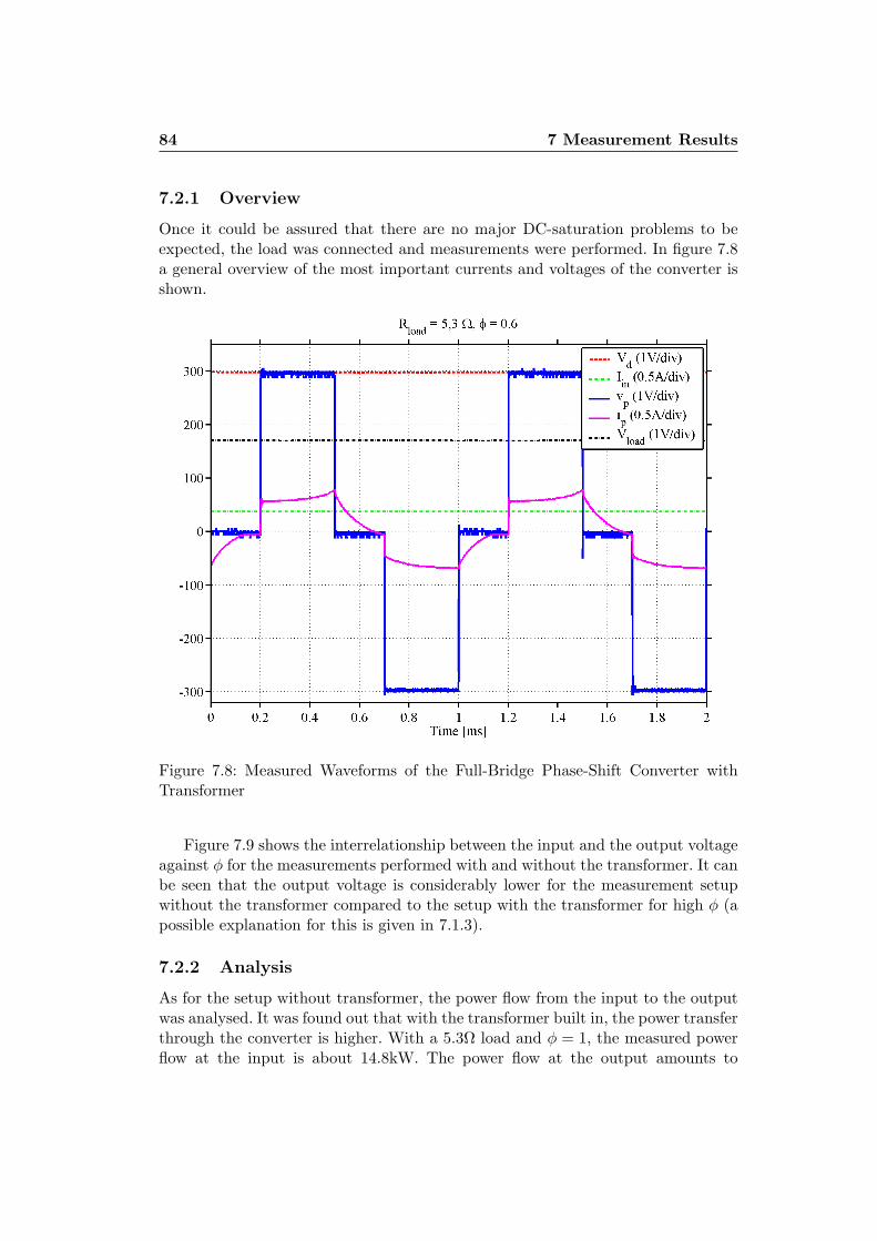
84 7 Measurement Results
7.2.1 Overview
Once it could be assured that there are no major DC-saturation problems to beexpected, the load was connected and measurements were performed. In figure 7.8a general overview of the most important currents and voltages of the converter isshown.
Figure 7.8: Measured Waveforms of the Full-Bridge Phase-Shift Converter withTransformer
Figure 7.9 shows the interrelationship between the input and the output voltageagainst φ for the measurements performed with and without the transformer. It canbe seen that the output voltage is considerably lower for the measurement setupwithout the transformer compared to the setup with the transformer for high φ (apossible explanation for this is given in 7.1.3).
7.2.2 Analysis
As for the setup without transformer, the power flow from the input to the outputwas analysed. It was found out that with the transformer built in, the power transferthrough the converter is higher. With a 5.3Ω load and φ = 1, the measured powerflow at the input is about 14.8kW. The power flow at the output amounts to
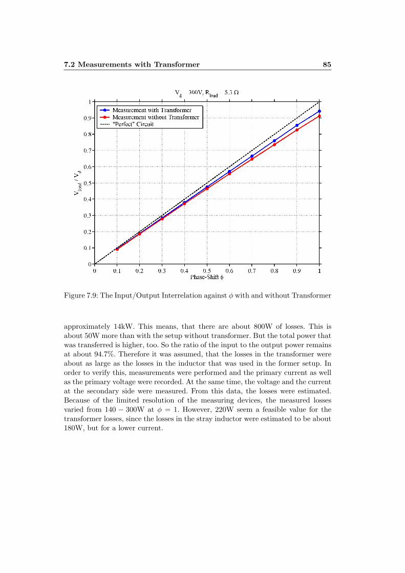
7.2 Measurements with Transformer 85
Figure 7.9: The Input/Output Interrelation against φ with and without Transformer
approximately 14kW. This means, that there are about 800W of losses. This isabout 50W more than with the setup without transformer. But the total power thatwas transferred is higher, too. So the ratio of the input to the output power remainsat about 94.7%. Therefore it was assumed, that the losses in the transformer wereabout as large as the losses in the inductor that was used in the former setup. Inorder to verify this, measurements were performed and the primary current as wellas the primary voltage were recorded. At the same time, the voltage and the currentat the secondary side were measured. From this data, the losses were estimated.Because of the limited resolution of the measuring devices, the measured lossesvaried from 140 − 300W at φ = 1. However, 220W seem a feasible value for thetransformer losses, since the losses in the stray inductor were estimated to be about180W, but for a lower current.


Chapter 8
Comparison of Measurementsand Simulations
The input/output relation of the converter is shown for the two simulations modelsand the two measurement setups in figure 8.1. One can see that for small φ the
Figure 8.1: The Input/Output Characteristic against φ
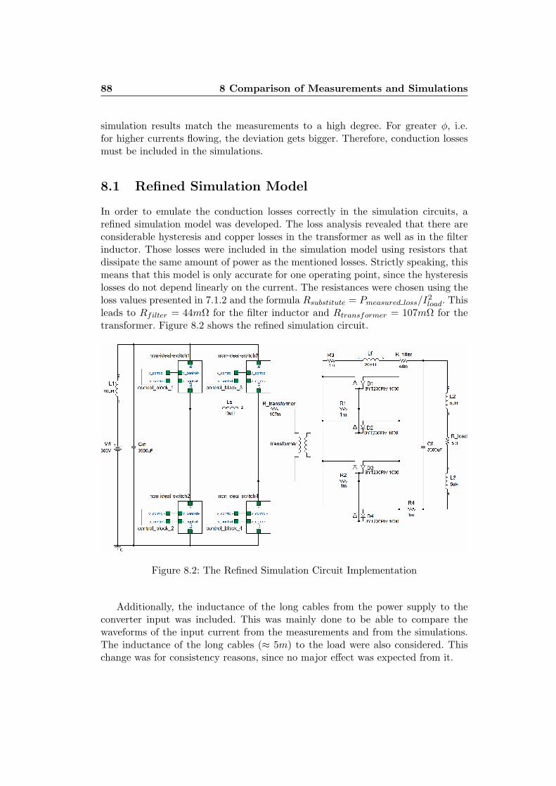
88 8 Comparison of Measurements and Simulations
simulation results match the measurements to a high degree. For greater φ, i.e.for higher currents flowing, the deviation gets bigger. Therefore, conduction lossesmust be included in the simulations.
8.1 Refined Simulation Model
In order to emulate the conduction losses correctly in the simulation circuits, arefined simulation model was developed. The loss analysis revealed that there areconsiderable hysteresis and copper losses in the transformer as well as in the filterinductor. Those losses were included in the simulation model using resistors thatdissipate the same amount of power as the mentioned losses. Strictly speaking, thismeans that this model is only accurate for one operating point, since the hysteresislosses do not depend linearly on the current. The resistances were chosen using theloss values presented in 7.1.2 and the formula Rsubstitute = Pmeasured loss/I2
load. Thisleads to Rfilter = 44mΩ for the filter inductor and Rtransformer = 107mΩ for thetransformer. Figure 8.2 shows the refined simulation circuit.
Figure 8.2: The Refined Simulation Circuit Implementation
Additionally, the inductance of the long cables from the power supply to theconverter input was included. This was mainly done to be able to compare thewaveforms of the input current from the measurements and from the simulations.The inductance of the long cables (≈ 5m) to the load were also considered. Thischange was for consistency reasons, since no major effect was expected from it.
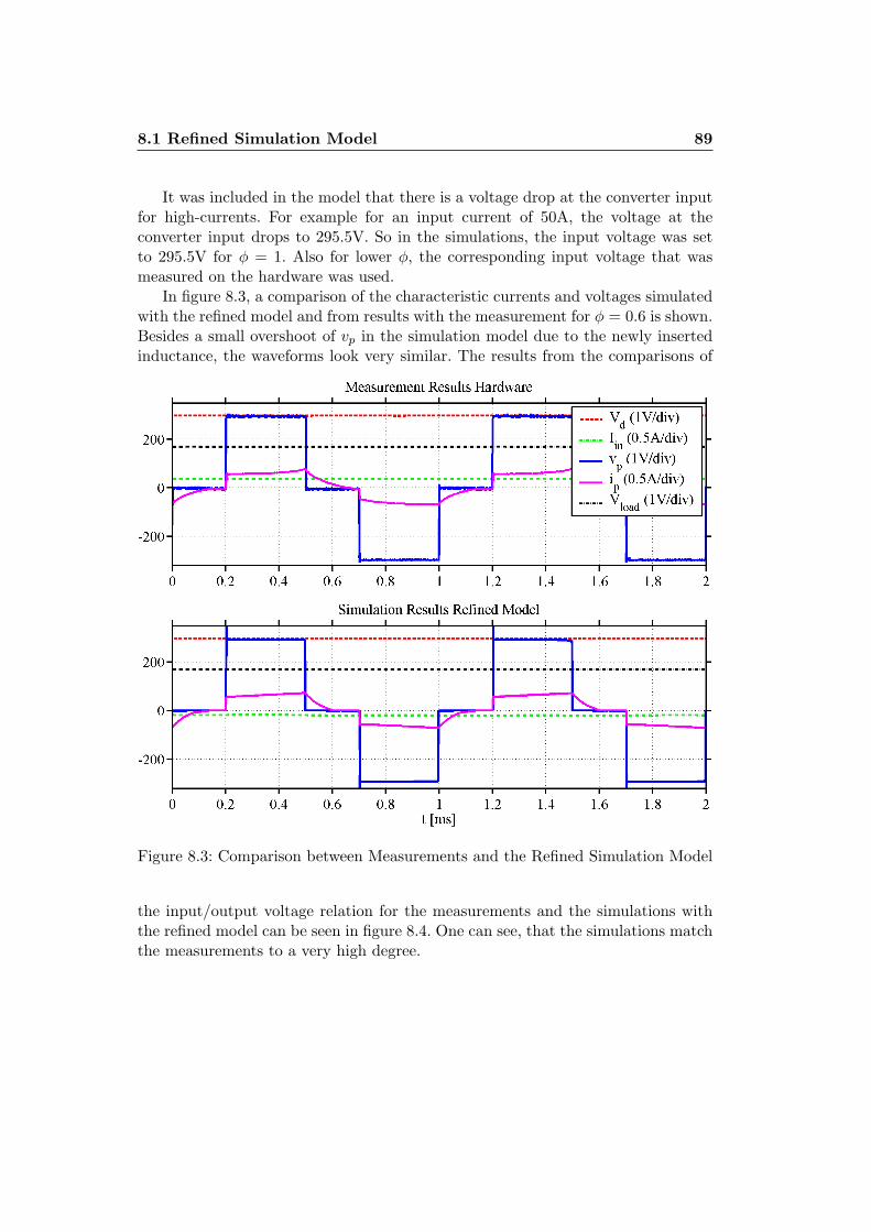
8.1 Refined Simulation Model 89
It was included in the model that there is a voltage drop at the converter inputfor high-currents. For example for an input current of 50A, the voltage at theconverter input drops to 295.5V. So in the simulations, the input voltage was setto 295.5V for φ = 1. Also for lower φ, the corresponding input voltage that wasmeasured on the hardware was used.
In figure 8.3, a comparison of the characteristic currents and voltages simulatedwith the refined model and from results with the measurement for φ = 0.6 is shown.Besides a small overshoot of vp in the simulation model due to the newly insertedinductance, the waveforms look very similar. The results from the comparisons of
Figure 8.3: Comparison between Measurements and the Refined Simulation Model
the input/output voltage relation for the measurements and the simulations withthe refined model can be seen in figure 8.4. One can see, that the simulations matchthe measurements to a very high degree.
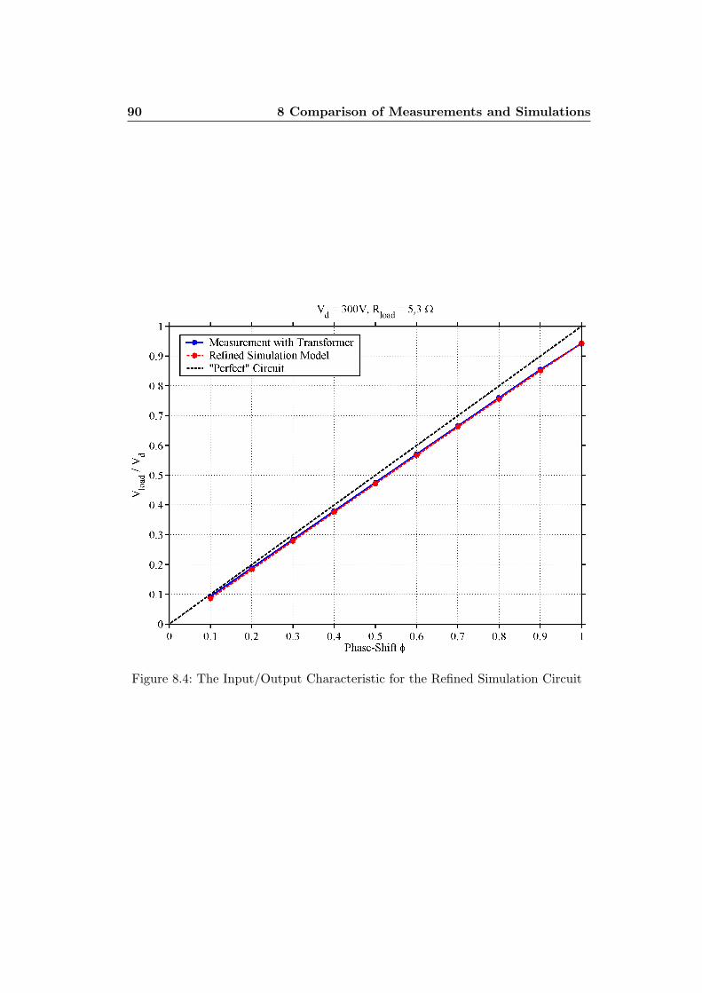
90 8 Comparison of Measurements and Simulations
Figure 8.4: The Input/Output Characteristic for the Refined Simulation Circuit

Chapter 9
Outlook and Conclusion
9.1 Conclusion
For the simulations it was found that the results can fully be explained by basicelectric circuit theory and by the theory introduced in the first part of this report.In addition, it was ascertained that the phase-shift controlled full-bridge DC-DCconverter has a linear behaviour for the relation of V load/V d against φ. This canbe concluded for both simulations and measurements. Furthermore, it was foundthat for the experimental setup that was built, the core and the copper losses ofthe transformer and the output filter inductor must be included in the simulationsto achieve accurate results. Because those losses show a linear dependency on thecurrent, they can be emulated using resistors that dissipate the same amount ofpower as the transformer/inductor in the measurements. With those modificationson the simulation model, the simulations match the measurements to a very highdegree.
For the two different experimental setups with and without transformer it canbe concluded that both of them show a power efficiency of about 94.7% for φ = 1.The efficiency increases then to about 96 − 97% for small φ. The results for smallφ however have to be interpreted with care, since the limited resolution of themeasuring devices has a greater influence on the results than for larger power flow.For the experimental setup without a transformer, it was detected that the convertershows a ”Buck”-like behaviour. That is to say, the output current is bigger than theinput current, also for φ = 1. The output voltage is therefore a bit lower than whatone would expect even though the overall power efficiency is the same as for thesetup with transformer.
So in conclusion it can be said, that a 15kW hardware model of the phase-shiftcontrolled full-bridge converter was built that is operative and may be of greatuse for further measurements. The converter may easily be extended unit by unitfor future research, since the hardware setup and its functionality are documentedin detail. Furthermore, a PSpice model was elaborated that simulates closely themeasurements performed on the converter. We have thus reached the goals we aimed
92 9 Outlook and Conclusion
at in our thesis.
9.2 Personal Retrospection
We have learned a lot during this thesis, both from a professional and from a per-sonal point of view. The elaboration of the software model was sometimes tedious.The simulations became though an interesting part of our work, once we got ac-customed to the peculiarities of PSpice. The hardware part of the work was aparticularly enriching experience, despite some problems related to the develop-ment of the setup. The completed converter ran smoothly at first try; this made upfor all the throwbacks we might have experienced during its assembly.
9.3 Future Work
A fully operative hardware model of the converter was built as well as a simulationmodel in PSpice. There are a few issues on which future research may want tofocus:
Hardware Control Some parts of the drive signal generation for the IGBTsshould be outsourced from software to hardware. Thus the phase-shift φ becomeschangeable in smaller steps than the step size of the dSPACE system (Ts = 50µs).Such as the drive signal generation is implemented now, φ can only be changed insteps of 10%. This leads to a very coarse resolution of the power flow. A smoothchange of φ is essential for the implementation of a controller; otherwise the con-troller can be omitted.
Moreover, it should ensured that the phases-shift changes exclusively after evernumbers of positive and negative voltage half-waves to prevent the risk of DC-saturation problems in the transformer. Also the duty ratio of the switches (i.e.the switch on-time) should be made changeable. For this purpose, the duty ratioshould be adjustable in small steps. The adjustment should be independent forthe switches providing the positive voltage and for the ones providing the negativevoltage. In that way one could compensate for possible DC-saturation problems ofthe transformer. But as we show in 7, no substantial problems with DC-saturationarise in normal operation.
Hardware Setup Some changes may improve the functionality of the hardwaresetup:
• Improve the mounting of the transformer. The dampening of the vibrationsof the transformer is presently not effective enough, therefore the transformergenerates a lot of noise during operation. Additionally, the cooling of thetransformer should be improved.

9.3 Future Work 93
• Place a switch for the fan on the front side of the rack in order to switch it onand off during operation. This should be done in order to facilitate thermalexperiments with the IGBTs.
• For expanded thermal measurements with the IGBTs, special resistors couldbe placed on the heatsink of the IGBTs in order to heat it up to a controlledtemperature. In this case, a temperature sensor should be integrated in theheatsink.
• A snubber circuit should be tested in order to reduce the switching losses inthe IGBTs. For the estimation of the optimum value for the capacitance, therefined PSpice simulation model could be used.
PSpice Circuit The findings concerning the simulation models of the phase-shift controlled full-bridge converter may also be applied to simulate other DC-DC converter types. There are several topologies that do not vary a lot from theimplemented converter in terms of hardware. It is only the control that differs.Therefore, one could investigate the accuracy of an adapted simulation model ofother types of converters.

Bibliography
[1] Mohan, Undeland, Robbins.: Power Electronics - Converters, Applications andDesign. John Wiley & Sons Inc., 3rd edition, 2003
[2] Demetriades, G.: On Small-Signal Analysis and Control of the Single- andDual-Active Bridge Topologies. Doctoral Thesis, 2005
[3] Max, L.: An investigation of different DC/DC-converters for wind farm appli-cations. Technical Report, 2005
[4] Kolar, J. W.: Grundlagen der Leistungselektronik. Lecture Notes, ETH Zurich,Power Electronic Systems Laboratory, 2005
[5] Demetriades, G. D.: Characterisation of the soft-switched single-active bridgetopology employing a novel control scheme for high-power dc-dc applications.Power Electronics Specialists, 2005 IEEE 36th Conference on , vol., no.pp.1947- 1951, June 12, 2005
[6] R.W.Erickson, D.Maksimovic: Fundamentals of Power Electronics. Massa-chusetts, USA: Kluwer Academic Publishers, 2nd edition, 2002
[7] Lena Max, Stefan Lundberg: System efficiency of a DC/DC converter basedwind turbine grid system. Nordic Wind Power Conference, ESPOO, FinlandMay 22-23, 2006
[8] ABB HVDC and HVDC Light. http://www.abb.com/hvdc
[9] Wikipedia Wind turbine. http://en.wikipedia.org/wiki/Wind turbine
[10] J.A.Sabate, V.Vlatkovic, R.B.Ridley, F.C.Lee and B.H.Cho Design Consider-ations for High-Voltage High-Power Full-Bridge Zero-Voltage-Switched PWMConverter IEEE Paper, 1990

Appendix A
Hardware Details
This appendix provides all hardware details of the parts used.
A.1 dSPACE
Some test were performed with the dSPACE hardware in order to investigate theirbehaviour, especially concerning synchronism of the different outputs. It was foundout that the four D/A outputs that are used for the drive signal generation arenot completely synchronous. There can be a delay of up to 0.5µs between thefirst and the last D/A output of the dSPACE system, see figure A.1. However,
Figure A.1: Rise and Fall Time of the Four D/A Outputs Used
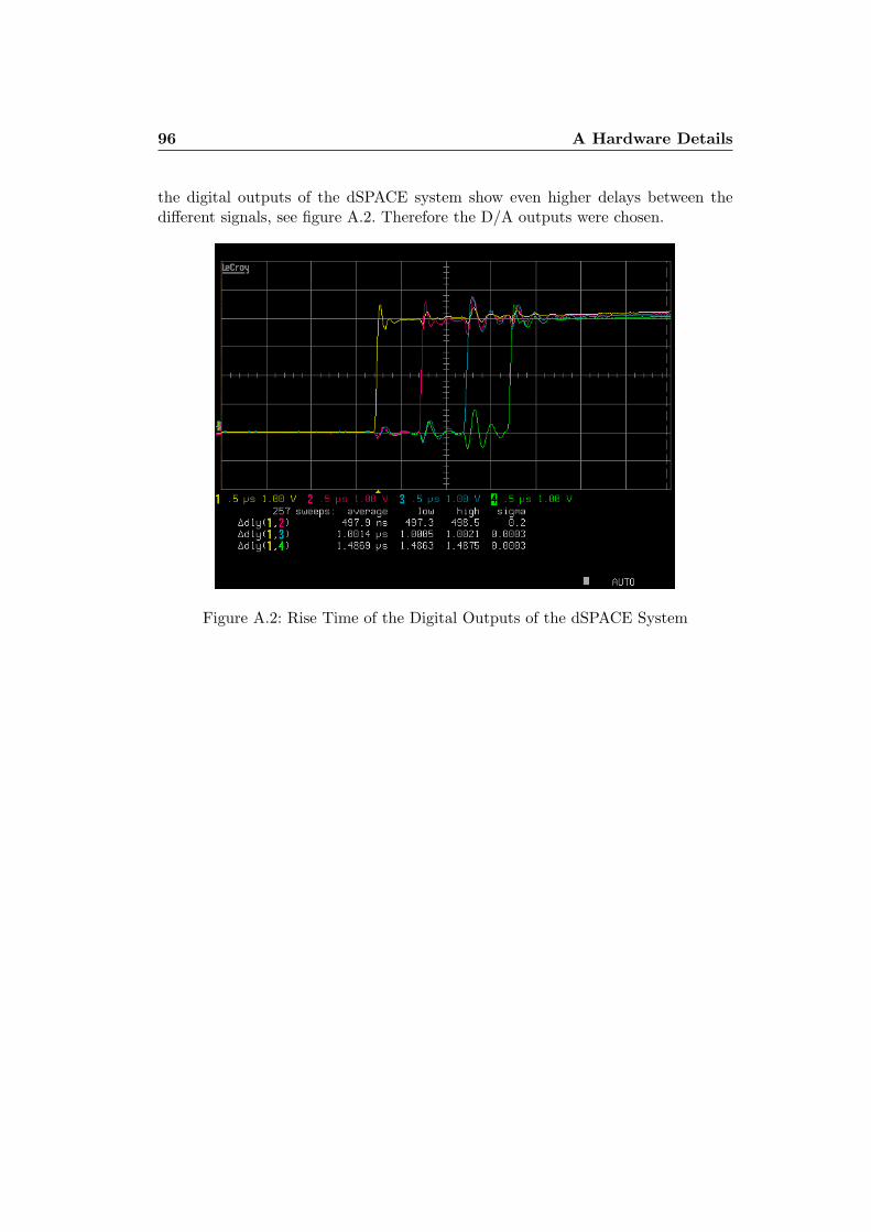
96 A Hardware Details
the digital outputs of the dSPACE system show even higher delays between thedifferent signals, see figure A.2. Therefore the D/A outputs were chosen.
Figure A.2: Rise Time of the Digital Outputs of the dSPACE System

A.2 Intermediate Card 1 97
Figure A.3: Schematics of the Intermediate Card 1
A.2 Intermediate Card 1
The intermediate card 1 is a connecting piece that maps the coaxial connectorscoming from the dSPACE output card to a 15-pin D-Sub connector that is used atthe input of the opto card. Table A.1 shows the pin mapping and figure A.3 givesa graphical overview of the card.
Table A.1: Pin Mapping on Intermediate Card 1
D-Sub Pin Coax. # Signal Description1 1 PWM1 drive signal for IGBT no. 12 2 PWM2 drive signal for IGBT no. 23 3 PWM3 drive signal for IGBT no. 34 4 PWM4 drive signal for IGBT no. 45 5 − spare6 6 − spare7 7 − spare8 − − not used9 − RESET reset opto card10 − DISABLE disable opto card11 8 DRIV ER BLOCKED readout status of opto card12 − GND signal ground13 − GND signal ground14 − GND signal ground15 − GND signal ground
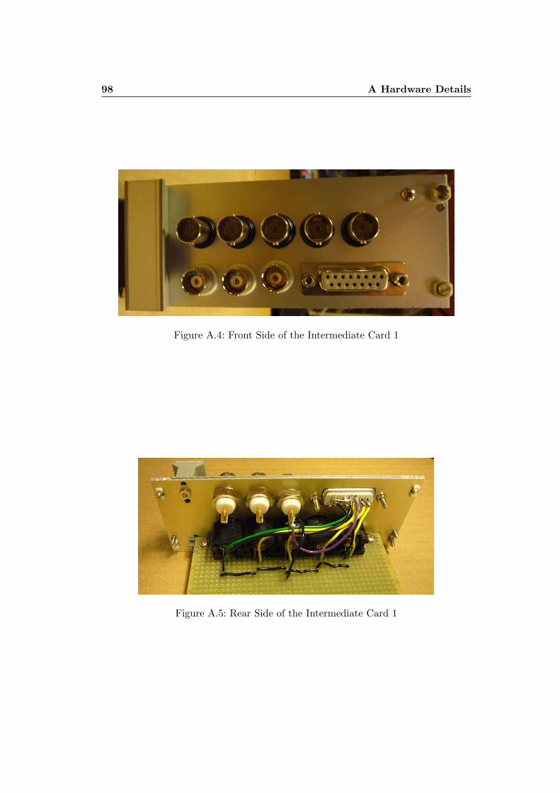
98 A Hardware Details
Figure A.4: Front Side of the Intermediate Card 1
Figure A.5: Rear Side of the Intermediate Card 1
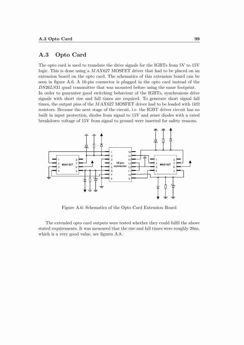
A.3 Opto Card 99
A.3 Opto Card
The opto card is used to translate the drive signals for the IGBTs from 5V to 15Vlogic. This is done using a MAX627 MOSFET driver that had to be placed on anextension board on the opto card. The schematics of this extension board can beseen in figure A.6. A 16-pin connector is plugged in the opto card instead of theDS26LS31 quad transmitter that was mounted before using the same footprint.In order to guarantee good switching behaviour of the IGBTs, synchronous drivesignals with short rise and fall times are required. To generate short signal falltimes, the output pins of the MAX627 MOSFET driver had to be loaded with 1kΩresistors. Because the next stage of the circuit, i.e. the IGBT driver circuit has nobuilt in input protection, diodes from signal to 15V and zener diodes with a ratedbreakdown voltage of 15V from signal to ground were inserted for safety reasons.
Figure A.6: Schematics of the Opto Card Extension Board
The extended opto card outputs were tested whether they could fulfil the abovestated requirements. It was measured that the rise and fall times were roughly 20ns,which is a very good value, see figures A.8.
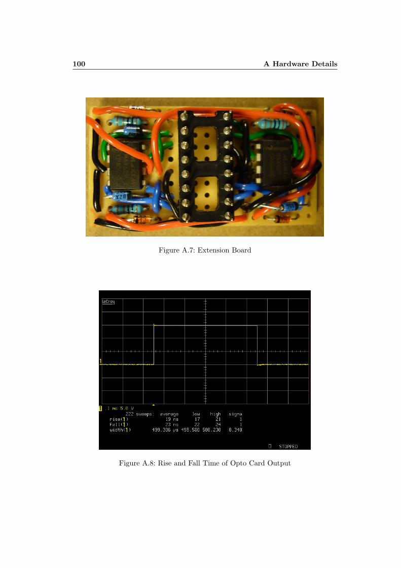
100 A Hardware Details
Figure A.7: Extension Board
Figure A.8: Rise and Fall Time of Opto Card Output

A.4 Intermediate Card 2 101
A.4 Intermediate Card 2
The intermediate card 2 is placed between the output of the opto card and theinput of the two driver circuits for the IGBTs. Two 20-pin ribbon cables are usedto connect each of the driver boards to the control circuit and to the power supplies(see datasheet of evaluation board). The appropriate pin assignment valid for thosecables can be seen in table A.2.
Four 2-pin plug-in terminals (S1-S4) are used for the connection of the drivesignals coming from the opto card. To avoid overvoltages on these signals due tothe inductance of the cable, 15V zener diodes were placed between the signal pinsand ground, see the schematic in figure A.9. Another two 2-pin plug-in terminals(P1, P2) accept the current for the driver circuits coming from a separate powersupply. A capacitor is placed between the 15V and the GND pin to stabilise thepower supply.
To read out the status signal of the IGBT driver board and forward it to theerror input of the opto card, a BNC connector (BNC1) is used. This signal is alsofed to the measure card over a 2-pin plug-in terminal (STATUS1) connected in par-allel to the BNC. A simple voltage divider was placed in front of the two outputs tolimit the status signal to 5V instead of 15V. To avoid a voltage drop on the signallines to the driver circuits due to the connections to the measure card and to theopto card, a MOSFET driver (M1) was placed in between those connections, seefigure ??.
The intermediate card 2 is also used to forward the temperature signal comingdirectly from one of the IGBT modules. Therefore, 3 more 2-pin terminals areplaced on it. One of them (P3) is to accept the necessary 15V from a auxiliarypower supply, another one (TEMP1) to connect to the IGBT module, and the lastone (TEMP2) to send the signal to the measure card.

102 A Hardware Details
Table A.2: Pin Assignment of Connectors to Driver Circuits on Intermediate Card2
Connector Pin # Signal Description1 15V power supply2 GND power supply3 15V power supply4 GND power supply5 15V power supply6 GND power supply7 n.c. not connected8 GND power supply9 Halt halt signal for IGBT (drivers)10 n.c. not connected11 n.c. not connected12 HaltGND halt signal ground13 n.c. not connected14 n.c. not connected15 PWM1 drive signal for IGBT no. 1 or 316 PWM2 drive signal for IGBT no. 2 or 417 n.c. not connected18 PWMGND drive signal ground19 n.c. not connected20 n.c. not connected
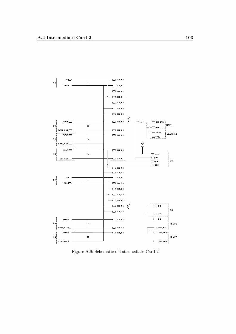
A.4 Intermediate Card 2 103
Figure A.9: Schematic of Intermediate Card 2
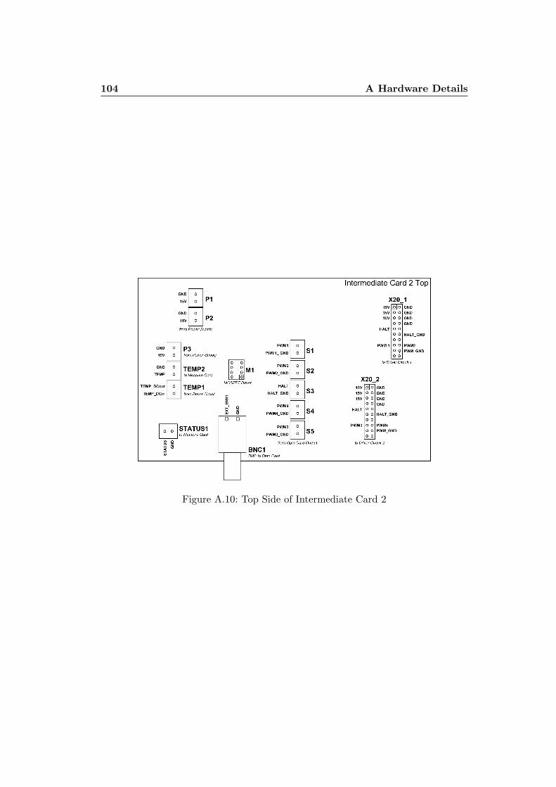
104 A Hardware Details
Figure A.10: Top Side of Intermediate Card 2

A.5 Evaluation Board 105
A.5 Evaluation Board
The connecting piece between the Skyper TM32Pro driver circuit and the rest ofthe circuit is the so-called EvaluationBoard1Skyper TM32Pro from Semikron. Intable A.3 the chosen equipment is shown. Note that there is the option of surfacedevice mounting (SMD) as well as conventional mounting for most adaption pos-sibilities. Wherever possible, the conventional mounting variant was chosen. TheSMD footprints were then not used. For detailed information please refer to thedatasheets of the Skyper32Pro driver circuit (esp. p.10-14) as well as of the evalu-ation board that can be found on the CD to this thesis or on www.semikron.com.The formulas used to calculate the value of the resistors and capacitors that weremounted on the evaluation board can also be found in those datasheets. If therewere no recommendations given in those datasheets, rules of thumb were used.
Table A.3: Evaluation Board Equipment
Connectors Value Name CommentX21, X22 o/c - interlock settings 3, 3µs (factory settings)X31, X32 o/c - interlock settings 3, 3µs (factory settings)X41, X42 o/c - interlock settings 3, 3µs (factory settings)X51, X52 o/c - interlock settings 3, 3µs (factory settings)X141, X142 18kΩ RCE dynamic short circuit protection TOPX151, X152 330pF CCE dynamic short circuit protection TOPX241, X242 18kΩ RCE dynamic short circuit protection BOTTOMX251, X252 330pF CCE dynamic short circuit protection BOTTOMR150 0Ω RV CE collector series resistance TOPR250 0Ω RV CE collector series resistance BOTTOMX111, X112 15Ω RGon gate on resistor TOPX131, X132 15Ω RGoff gate off resistor TOPX211, X212 15Ω RGon gate on resistor BOTTOMX231, X232 15Ω RGoff gate off resistor BOTTOMX161, X162 o/c RGoff SC soft turn-off TOP (not used)X261, X262 o/c RGoff SC soft turn-off BOTTOM (not used)X171, X172 330Ω R172 over temp. protection, shut down @> 115 CX181, X182 39Ω1 R177 over temp. protection, shut down @> 115 C
1For the calculation of this value, the resistance @−40 C for the NTC resistor was assumed tobe about 11kΩ. Refer also to the datasheet of the IGBT that can be found on the CD enclosedwith this report.

106 A Hardware Details
A.6 Voltage Transducer Card
As mentioned in 5.2.2, the voltage transducer card was used to measure the inputand the output voltage of the DC-DC converter. Those voltages can have spikesup to 350V . The card was designed such that it could handle three different in-put voltages, each of them in a range of ±600V . In a first step, these voltages aretransformed down to ±1V with a voltage divider, consisting of R1-R4 and R13 infigure A.11. These signals are then fed into a AD210. This is a high performanceisolation amplifier that provides complete galvanic isolation. The gain between in-and output can be adjusted with a potentiometer P1. It was chosen as G = 10,thus the output range of the card amounts to ±10V . Thereby, the output signalscan be processed by the measurement system dSPACE via the measure card.
All the in- and outputs as well as the power supply for the AD210 are attachedto the voltage transducer card over a 32-pin euro-connector. The corresponding pinassignment can be seen in table A.4.
Table A.4: Pin Assignment on Voltage Transducer Card
Pin Signal Description2d Ch1Out channel 1 out2b Ch2Out channel 2 out2z Ch3Out channel 3 out4 n.c. not connected6 n.c. not connected8 n.c. not connected10 n.c. not connected12 15V power supply14 GND power supply16 −15V power supply18 n.c. not connected20 Ch1in channel 1 in +22 Ch1in channel 1 in -24 Ch2in channel 2 in +26 Ch2in channel 2 in -28 Ch3in channel 3 in +30 Ch3in channel 3 in -32 n.c. not connected
Calculations As mentioned above, the voltage transducer card was designed suchthat it can handle input voltages in a range of VinCard = ±600V. The therefore nec-essary adjustments on the input side of the AD210 are explained with the followingcalculations. For further details please refer to the corresponding datasheet of the

A.6 Voltage Transducer Card 107
Figure A.11: Schematic of Voltage Transducer Card
AD210.The gain of the input of the AD210 can be calculated with:
VoutAD210 = VinAD210(1 + (R16 + P1
R19)). (A.1)
Approach: R19 = 5.64kΩ, R16 = 47.5kΩ, P1 = 5kΩ. This yields to:
VoutAD210 = VinAD210 ·G = VinAD210 · 10.3 (A.2).
The desired output voltage range to measure system (i.e. measure card) is:VoutCard = VoutAD210 = ±10V.
With G=10 in equation A.2 the output of the voltage divider at the input ofthe card results in VinAD210 = ±1V:
VinAD210
VinCard=
R13R13 + R1 + R2 + R3 + R4
=1
600. (A.3)
Chosen value for R1, R2, R3 and R4 = 121kΩ. Therefore:VinAD210
VinCard=
R13R13 + 484kΩ
≈ R13484kΩ
. (A.4)
This yields to:
R13 =484000Ω
600= 806.66Ω. (A.5)
Because only 806Ω resistors are available, R13 = 806Ω was chosen.The dissipated power in resistances R1−R4 can be calculated with:
Iin =VinCard
Rtot=
601.5V
484000 + 806= 1.25mA (A.6)
PR = 121000 · 0.001252 = 0.18W. (A.7)
The chosen metal film resistors can handle a power of 0.6W, so there should not beany problems.

108 A Hardware Details
Table A.5: Values of Parts on Voltage Transducer Card
Part ValueR1−R12 121kΩR13−R15 806ΩR16−R18 47.5kΩR19−R21 5.64kΩR22−R24 200ΩR25−R27 51kΩP1−P3 5kΩP4−P6 100kΩC7−C8 100µFC9−C11 0.1µFD7−D8 1N4007

A.7 Measure Card 109
A.7 Measure Card
For all measurements that were made with dSPACE, the measure card was usedas connecting piece. The measure card protects the dSPACE inputs and translatesthe measurement signals that are currents to voltages. In table A.6 the chosenequipment is shown. A BNC connector is used for the connection of the error signalto the opto card. Another 10 BNC connectors mounted on the front plate of thecard can be used to send the measured signals with coax cables to the dSPACEsystem.
Output Filter of Measured Signals The impedance of the output filter to-wards the dSPACE system can be calculated as:
Z ≈√
R/C =√
10kΩ/100nF ≈ 316kΩ (A.8)
The input impedance of the dSPACE system is about 1MΩ, so the calculatedoutput impedance is acceptable.
LEM Modules The maximum allowed measurement resistance RM of the LEMLA100− S is 100Ω. For the LEM LT300− S the maximum allowed measurementresistance RM is 51Ω. With a turns ratio of 1 : 2000 (for both LEM module types)and a maximum expected current of 50A, this results in 0− 2.5V (and 0− 1.25V,respectively) input voltage for the dSPACE system. This is good enough since thedSPACE inputs possess a resolution of 16bit over the voltage range of ±10V .
Temperature Measurement The IGBT built-in NTC temperature sensor thatis used to monitor the thermal state of the IGBT modules has a minimum resistanceRT min of 330Ω in the allowed temperature range. In order to have an optimisedmeasuring range, the measurement resistance was chosen using the following calcu-lations:
RmeasVmeas
Rmeas + RT min=
Rmeas15V
Rmeas + 330Ω= VdSPACE in max ≡ 10V (A.9)
⇒ Rmeas = 660Ω; next available: 620Ω

110 A Hardware Details
Table A.6: Measure Card Equipment
Designator Value DescriptionR1 100Ω RM LEM1R2 100Ω RM LEM3R3 51Ω RM LEM2R4 10kΩ Voltage Transducer Card Channel 1R5 10kΩ Voltage Transducer Card Channel 2R6 10kΩ Voltage Transducer Card Channel 3R7 10kΩ IGTB statusR8 620Ω temperature measurementR9 10kΩ spareR10 10kΩ spareR11−R20 10kΩ output filter towards dSPACER21−R30 o/c optional second output filter configurationC1− C10 100nF output filter towards dSPACE

A.8 Heatsink for Rectifier Bridge 111
A.8 Heatsink for Rectifier Bridge
Due to conduction and switching losses, the four diodes used for the output rectifierbridge can get very hot during operation. In order to protect them against thermaldestruction, a heatsink is used for cooling. The following calculations were made:According to [1] the maximum junction-to-ambient thermal resistance RΘ,ja can beestimated as
RΘ,ja =(Tj,max − Ta,max)
PLoss. (A.10)
The maximum acceptable junction temperature Tj,max of the diodes is 150 C, asgiven in the data sheet. The maximum ambient temperature is assumed to be 30 C.PLoss is made up of the sum of the conduction losses and the switching losses.Because of the low switching frequency of 1kHz the second part can be neglected:
PLoss = Pconduction + Pswitching ≈ Pconduction. (A.11)
According to the data sheet of the diodes, Pconduction can be calculated as: @TODO:reference
Pconduction = 1.47 · IF,(AV ) + 0.01 · I2F,(RMS). (A.12)
The forward-current flowing through every dual-diode during half a switchingperiod is equal to the output current through the load which is at maximum 50A.Thus, one single diode has to conduct 25A during 0.5ms. Therefore, the averagevalue of this current IF,(AV ) is 0.5 · 25A = 12.5A.
The next step is to calculate IF,(RMS):
IF,(RMS) =
√1
(T2 − T1)
∫ T2
T1
[f(t)]2 · dt (A.13)
=√
11
1000
[∫ 1
20000 0 · dt +
∫ 110001
2000
252 · dt] =√
312.5A ≈ 18A.
The conduction loss per diode is consequently:
Pconduction = 1.47 · 12.5A + 0.01 · 182 ≈ 22W. (A.14)
This yields to a maximum conduction loss in the output rectifier bridge of8 · 22W = 176W . By inserting these values into formula A.10 one obtains a junction-to-ambient thermal resistance RΘ,ja = 0.682
CW .
According to figure A.12, RΘ,ja = RΘ,jc +RΘ,cs +RΘ,sa. The thermal resistancebetween junction and case RΘ,jc as well as between case and sink RΘ,cs can befound with the values in the data sheets and by calculation of the total parallelresistances. Hence the value of RΘ,sa should be:
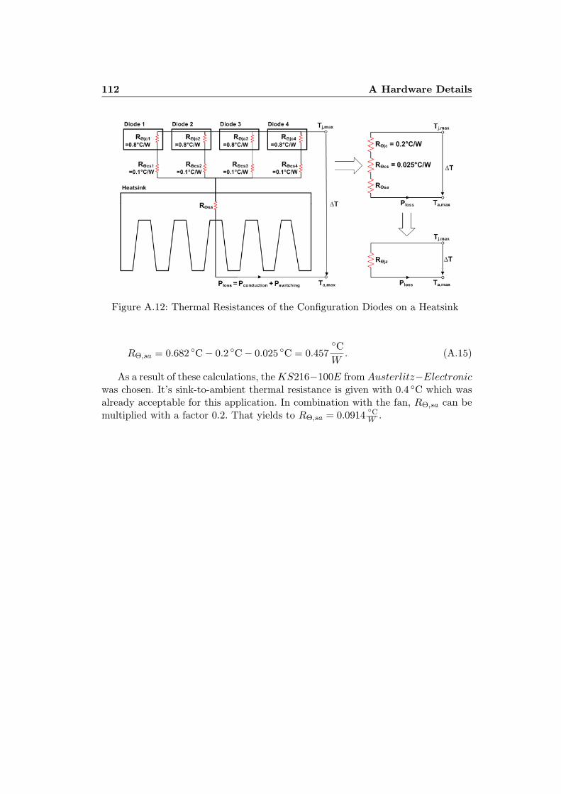
112 A Hardware Details
Figure A.12: Thermal Resistances of the Configuration Diodes on a Heatsink
RΘ,sa = 0.682 C− 0.2 C− 0.025 C = 0.457CW
. (A.15)
As a result of these calculations, the KS216−100E from Austerlitz−Electronicwas chosen. It’s sink-to-ambient thermal resistance is given with 0.4 C which wasalready acceptable for this application. In combination with the fan, RΘ,sa can bemultiplied with a factor 0.2. That yields to RΘ,sa = 0.0914
CW .

A.9 Output Filter Design 113
A.9 Output Filter Design
For an input voltage of 300V, the voltage at the output filter input can changemaximally by 150V during one fourth of the switching period, i.e. for 0.25ms. Ifthe current ripples at the output must not become too big, the output inductancehas to be several mH. For the desired maximum current of 50 amperes the inductorbecomes too big to mount on a plate. So an existing free-standing inductor waschosen that has an inductance of 20mH and can handle a current of up to 80amperes. For this inductor, the following maximum current ripple can be calculated:
δISmax =Vd/2LS
dt =150V
20mH0.25mS = 1.875A. (A.16)
Due to this small current ripple, the output capacitor can be chosen rather small.A 3, 3µF capacitor was chosen, so the resulting cut off frequency is:
Fcutoff =1
2π√
LSCS=
12π√
20mH3.3mF≈ 20Hz. (A.17)

114 A Hardware Details
A.10 Cables
Unless otherwise noted, all connections of the power components were done usingcopper cables with 6mm intersection. This results in a maximum current density of
Smax =Imax
πr2=
50A
π(3mm)2= 1.77A/mm2. (A.18)
This value for the maximum current density is acceptable.

A.11 Power Supply 115
A.11 Power Supply
The driver circuits make high demands on their power source:
• supply voltage: +15V ±4%
• maximum trise of supply voltage: 50ms
• continuous supply voltage rising slope
• minimum Ipeak: 1A
Hence, a power supply unit was chosen that is able to provide at least 2A (infact 3.2A) output current at +15V. Furthermore some measurements were done todemonstrate that the other required features can be achieved. The power supply wasconnected to a LeCroy digital oscilloscope and then turned on. The startup voltage-transients were displayed on the oscillograph and the data stored and analysed.Figure A.13 shows the obtained voltage waveforms. As can be seen, the voltagereaches the 15V level ≈ 14ms after turn-on and the rising slope is continuous. Thusit results that this power supply can be used.
Figure A.13: Voltage Waveform during Start-up

116 A Hardware Details
Figure A.14: Power Supply
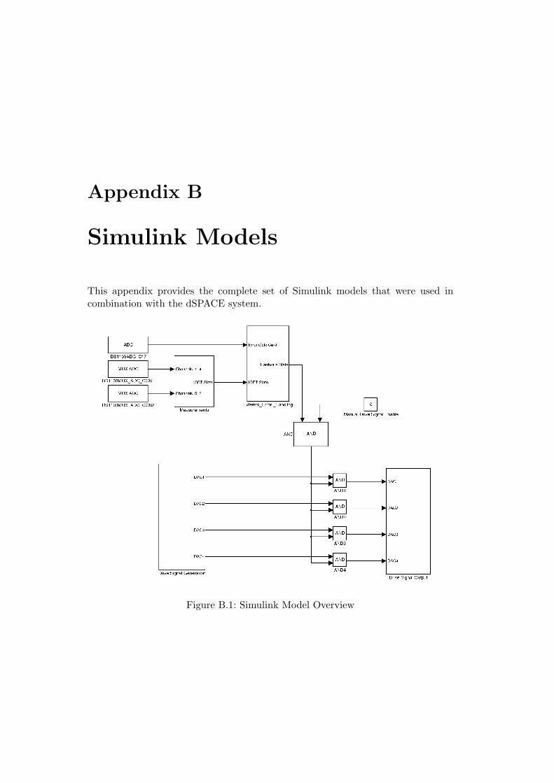
Appendix B
Simulink Models
This appendix provides the complete set of Simulink models that were used incombination with the dSPACE system.
Figure B.1: Simulink Model Overview
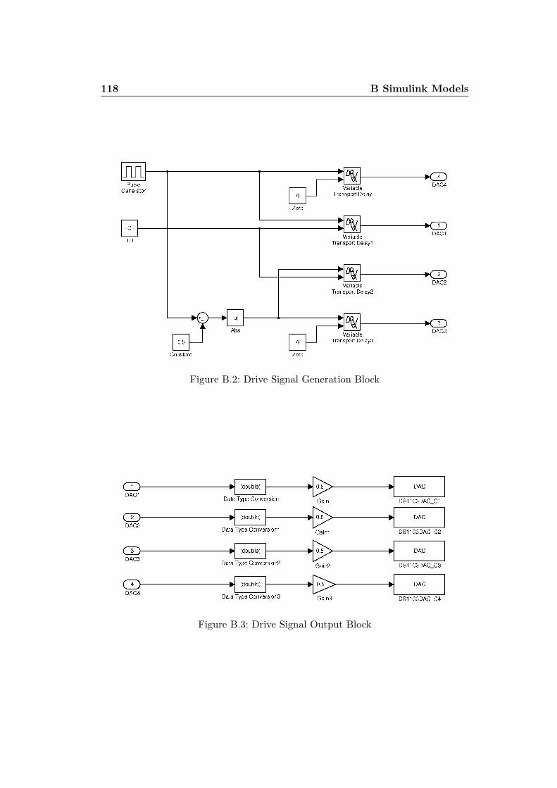
118 B Simulink Models
Figure B.2: Drive Signal Generation Block
Figure B.3: Drive Signal Output Block
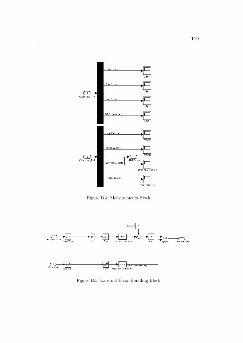
119
Figure B.4: Measurements Block
Figure B.5: External Error Handling Block