Embed Size (px)
Citation preview
MOTOROLA
Semiconductor Application Note
AN1764/DRev. #1.0
© Motorola, Inc., 1998
DS
P56
300
ES
SI P
rogr
amm
ing
DSP56300 Enhanced Synchronous Serial Interface (ESSI) Programming
By Tina M. Redheendran
The Enhanced Synchronous Serial Interface (ESSI) provides a full-duplex serial port for communicating with a variety of serial devices. The ESSI comprises independent transmitter and receiver sections and a common ESSI clock generator. Three transmit shift registers enable it to transmit from three different pins simultaneously. It interfaces to TDM networks without additional logic. Each DSP56300 family device includes two ESSIs and thus can accommodate six total ESSI transmitters for six channel surround sound applications.
This document consists of two sections. The first surveys the pins and registers that control ESSI operation. The second describes how the ESSI operates and includes small segments of code that illustrate practical programming guidelines.
Contents
Part I: ESSI Architecture ........ 2
1.1 ESSI Pins .............................31.2 ESSI Registers .....................4
Part II: ESSI Programming ... 11
2.1 Transfer Characteristics .....112.1.1 Word Length......................112.1.2 Word Alignment ................112.1.3 Shift Direction ...................122.2 Synchronization Signals ....132.2.1 Synchronous Versus
Asynchronous ....................132.2.2 Clock Signal.......................142.2.3 Frame Sync ........................142.2.4 Flags...................................152.3 Operation Modes ...............152.3.1 Normal Mode.....................162.3.2 Network Mode ...................162.3.2.1 Time Slot Register .............172.3.2.2 Transmit Slot Mask
Registers ............................172.3.2.3 Receive Slot Mask
Registers ............................172.3.2.4 On-Demand Mode .............182.4 Programming Control
Registers ............................182.4.1 Example 1 ..........................182.4.2 Example 2 ..........................192.5 Initialization.......................202.6 Transfer Methods...............212.6.1 Polling................................212.6.2 Interrupts............................222.6.3 DMA..................................232.7 References..........................25
Motorola DSP56300 ESSI Programming 2
Part 1 ESSI Architecture
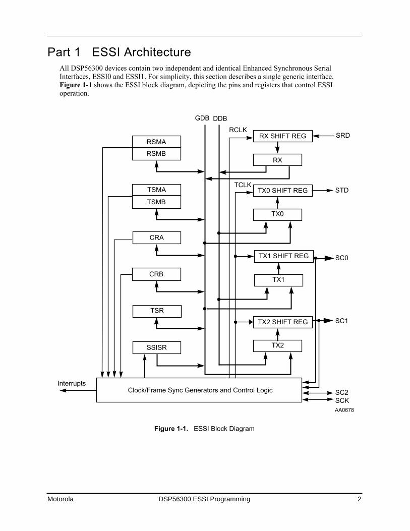
All DSP56300 devices contain two independent and identical Enhanced Synchronous Serial Interfaces, ESSI0 and ESSI1. For simplicity, this section describes a single generic interface.
Figure 1-1
shows the ESSI block diagram, depicting the pins and registers that control ESSI operation.
Figure 1-1.
ESSI Block Diagram
RSMA
RSMB
TSMA
TSMB
SSISR
RX
RX SHIFT REG
TX0 SHIFT REG
TSR
RCLK
TX0
CRB
CRA
SRD
STDTCLK
SC2SCK
Clock/Frame Sync Generators and Control LogicInterrupts
GDB DDB
TX1 SHIFT REG
TX1
SC0
TX2 SHIFT REG
TX2
SC1
AA0678
ESSI Pins
Motorola ESSI Architecture 3
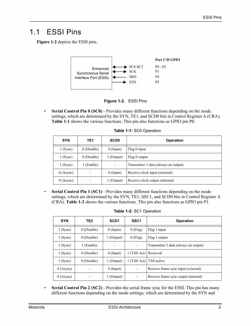
1.1 ESSI Pins
Figure 1-2
depicts the ESSI pins.
Figure 1-2.
ESSI Pins
¥
Serial Control Pin 0 (SC0)
- Provides many different functions depending on the mode settings, which are determined by the SYN, TE1, and SCD0 bits in Control Register A (CRA).
Table 1-1
shows the various functions. This pin also functions as GPIO pin P0.
¥
Serial Control Pin 1 (SC1)
- Provides many different functions depending on the mode settings, which are determined by the SYN, TE1, SSC1, and SCD0 bits in Control Register A (CRA).
Table 1-2
shows the various functions. This pin also functions as GPIO pin P1.
¥
Serial Control Pin 2 (SC2)
- Provides the serial frame sync for the ESSI. This pin has many different functions depending on the mode settings, which are determined by the SYN and
Table 1-1:
SC0 Operation
SYN TE1 SCD0 Operation
1 (Sync) 0 (Disable) 0 (Input) Flag 0 input
1 (Sync) 0 (Disable) 1 (Output) Flag 0 output
1 (Sync) 1 (Enable) - Transmitter 1 data (always an output)
0 (Async) - 0 (Input) Receive clock input (external)
0 (Async) - 1 (Output) Receive clock output (internal)
Table 1-2:
SC1 Operation
SYN TE2 SCD1 SSC1 Operation
1 (Sync) 0 (Disable) 0 (Input) 0 (Flag) Flag 1 input
1 (Sync) 0 (Disable) 1 (Output) 0 (Flag) Flag 1 output
1 (Sync) 1 (Enable) - - Transmitter 2 data (always an output)
1 (Sync) 0 (Disable) 0 (Input) 1 (TX0 Act) Reserved
1 (Sync) 0 (Disable) 1 (Output) 1 (TX0 Act) TX0 active
0 (Async) - 0 (Input) - Receive frame sync input (external)
0 (Async) - 1 (Output) - Receive frame sync output (internal)
EnhancedSynchronous Serial
Interface Port (ESSI)
SC0-SC2SCK
SRD
STD
P0 - P2P3
P4
P5
Port C/D GPIO
Motorola DSP56300 ESSI Programming 4
ESSI Registers
SCD2 bits in Control Register A (CRA).
Table 1-3
shows the various functions. This pin also functions as GPIO pin P2.
¥
Serial Clock Pin (SCK)
- Provides the serial bit rate clock for the ESSI. This pin has many different functions depending on the mode settings, which are determined by the SYN and SCKD bits in Control Register A (CRA).
Table 1-4
shows the various functions. This pin also functions as GPIO pin P3.
¥
Serial Receive Data Pin (SRD)
- Receives data and is always an input. This pin also functions as GPIO pin P4.
¥
Serial Transmit Data Pin (STD)
- Transmits data from transmitter 0 and is always an output. This pin also functions as GPIO pin P5.
1.2 ESSI Registers
The following registers control ESSI operation:
¥
Control Register A (CRA)
Ñ One of two registers that control ESSI operation (see
Table 1-5
).
¥
Control Register B (CRB) Ñ
Second of two registers that control ESSI operation (see
Table 1-6
).
¥
Status Register (SSISR)
Ñ A read-only register that describes the ESSI status and serial flags (see
Table 1-7
).
¥
Transmit Slot Mask Register A (TSMA)
and
Transmit Slot Mask Register B (TSMB) Ñ
Two registers that, in network mode, determine whether to transmit during a given time slot or to tri-state the transmitter. TSMA and TSMB together form one register, TSM. When bit
n
of TSM is cleared, the transmit data pins of the enabled transmitters are tri-stated during time slot
n
. When bit
n
of TSM is set, the transmit sequence proceeds normally during time slot
n
.
Table 1-3:
SC2 Operation
SYN SCD2 Operation
1 (Sync) 0 (Input) Transmit and receive frame sync input (external)
1 (Sync) 1 (Output) Transmit and receive frame sync output (internal)
0 (Async) 0 (Input) Transmit frame sync input (external)
0 (Async) 1 (Output) Transmit frame sync output (internal)
Table 1-4:
SCK Operation
SYN SCKD Operation
1 (Sync) 0 (Input) Transmit and receive clock input (external)
1 (Sync) 1 (Output) Transmit and receive clock output (internal)
0 (Async) 0 (Input) Transmit clock input (external)
0 (Async) 1 (Output) Transmit clock output (internal)
ESSI Registers
Motorola ESSI Architecture 5
¥
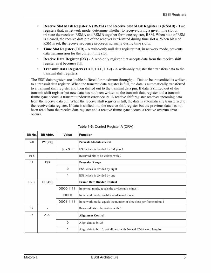
Receive Slot Mask Register A (RSMA)
and
Receive Slot Mask Register B (RSMB)
- Two registers that, in network mode, determine whether to receive during a given time slot or tri-state the receiver. RSMA and RSMB together form one register, RSM. When bit
n
of RSM is cleared, the receive data pin of the receiver is tri-stated during time slot
n
. When bit
n
of RSM is set, the receive sequence proceeds normally during time slot
n
.
¥
Time Slot Register (TSR)
- A write-only null data register that, in network mode, prevents data transmission for the current time slot.
¥
Receive Data Register (RX)
- A read-only register that accepts data from the receive shift register as it becomes full.
¥
Transmit Data Registers (TX0, TX1, TX2)
- A write-only register that transfers data to the transmit shift registers.
The ESSI data registers are double buffered for maximum throughput. Data to be transmitted is written to a transmit data register. When the transmit data register is full, the data is automatically transferred to a transmit shift register and then shifted out to the transmit data pin. If data is shifted out of the transmit shift register but new data has not been written to the transmit data register and a transmit frame sync occurs, a transmit underrun error occurs. A receive shift register receives incoming data from the receive data pin. When the receive shift register is full, the data is automatically transferred to the receive data register. If data is shifted into the receive shift register but the previous data has not been read from the receive data register and a receive frame sync occurs, a receive overrun error occurs.
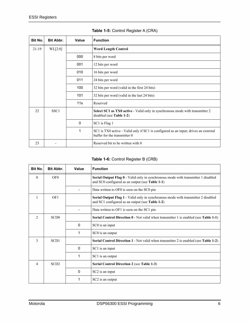
Table 1-5:
Control Register A (CRA)
Bit No. Bit Abbr. Value Function
7-0 PM[7:0]
Prescale Modulus Select
$0 - $FF
ESSI clock is divided by PM plus 1
10-8 - Reserved bits to be written with 0
11 PSR
Prescaler Range
0
ESSI clock is divided by eight
1
ESSI clock is divided by one
16-12 DC[4:0]
Frame Rate Divider Control
00000-11111
In normal mode, equals the divide ratio minus 1
00000
In network mode, enables on-demand mode
00001-11111
In network mode, equals the number of time slots per frame minus 1
17 - Reserved bits to be written with 0
18 ALC
Alignment Control
0
Align data to bit 23
1
Align data to bit 15, not allowed with 24- and 32-bit word lengths
Motorola DSP56300 ESSI Programming 6
ESSI Registers
21-19 WL[2:0]
Word Length Control
000
8 bits per word
001
12 bits per word
010
16 bits per word
011
24 bits per word
100
32 bits per word (valid in the first 24 bits)
101
32 bits per word (valid in the last 24 bits)
11x
Reserved
22 SSC1
Select SC1 as TX0 active
- Valid only in synchronous mode with transmitter 2 disabled (see
Table 1-2
)
0
SC1 is Flag 1
1
SC1 is TX0 active - Valid only if SC1 is configured as an input; drives an external buffer for the transmitter 0
23 - Reserved bit to be written with 0
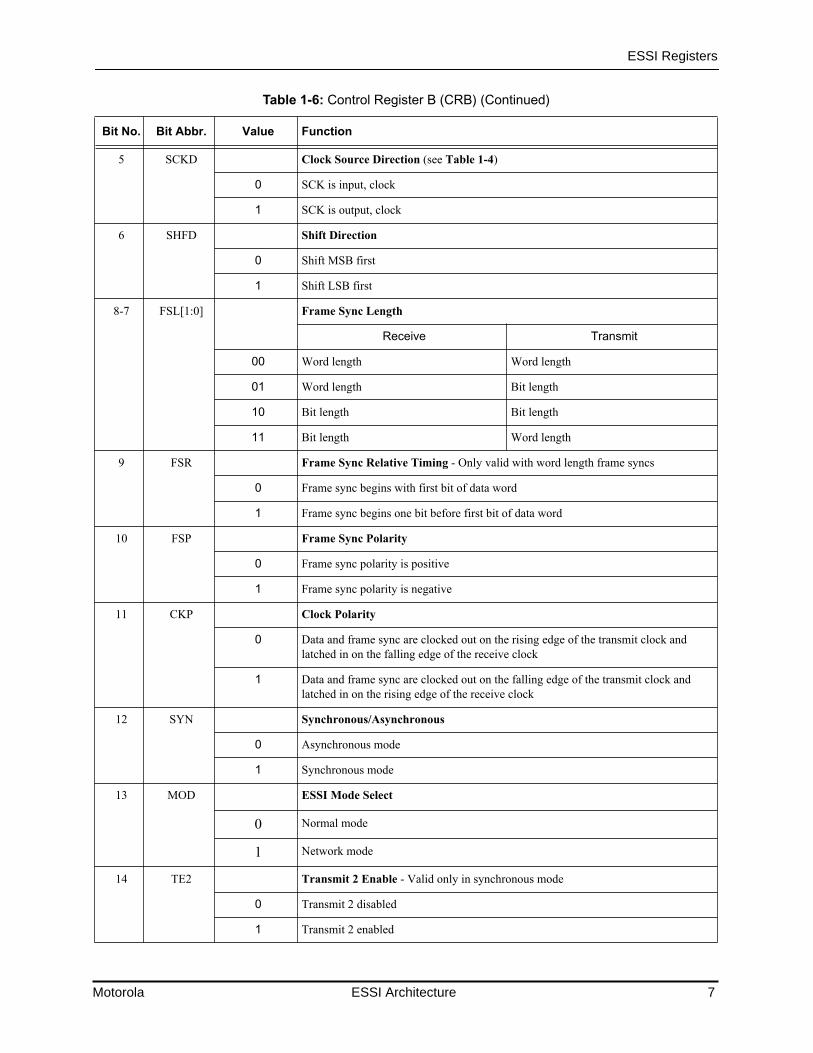
Table 1-6:
Control Register B (CRB)
Bit No. Bit Abbr. Value Function
0 OF0
Serial Output Flag 0
- Valid only in synchronous mode with transmitter 1 disabled and SC0 configured as an output (see
Table 1-1
)
-
Data written to OF0 is seen on the SC0 pin
1 OF1
Serial Output Flag 1
- Valid only in synchronous mode with transmitter 2 disabled and SC1 configured as an output (see
Table 1-2
)
-
Data written to OF1 is seen on the SC1 pin
2 SCD0
Serial Control Direction 0
- Not valid when transmitter 1 is enabled (see
Table 1-1
)
0
SC0 is an input
1
SC0 is an output
3 SCD1
Serial Control Direction 1
- Not valid when transmitter 2 is enabled (see
Table 1-2
)
0
SC1 is an input
1
SC1 is an output
4 SCD2
Serial Control Direction 2
(see
Table 1-3
)
0
SC2 is an input
1
SC2 is an output
Table 1-5:
Control Register A (CRA)
Bit No. Bit Abbr. Value Function
ESSI Registers
Motorola ESSI Architecture 7
5 SCKD
Clock Source Direction
(see
Table 1-4
)
0
SCK is input, clock
1
SCK is output, clock
6 SHFD
Shift Direction
0
Shift MSB first
1
Shift LSB first
8-7 FSL[1:0]
Frame Sync Length
Receive Transmit
00
Word length Word length
01
Word length Bit length
10 Bit length Bit length
11 Bit length Word length
9 FSR Frame Sync Relative Timing - Only valid with word length frame syncs
0 Frame sync begins with first bit of data word
1 Frame sync begins one bit before first bit of data word
10 FSP Frame Sync Polarity
0 Frame sync polarity is positive
1 Frame sync polarity is negative
11 CKP Clock Polarity
0 Data and frame sync are clocked out on the rising edge of the transmit clock and latched in on the falling edge of the receive clock
1 Data and frame sync are clocked out on the falling edge of the transmit clock and latched in on the rising edge of the receive clock
12 SYN Synchronous/Asynchronous
0 Asynchronous mode
1 Synchronous mode
13 MOD ESSI Mode Select
0 Normal mode
1 Network mode
14 TE2 Transmit 2 Enable - Valid only in synchronous mode
0 Transmit 2 disabled
1 Transmit 2 enabled
Table 1-6: Control Register B (CRB) (Continued)
Bit No. Bit Abbr. Value Function
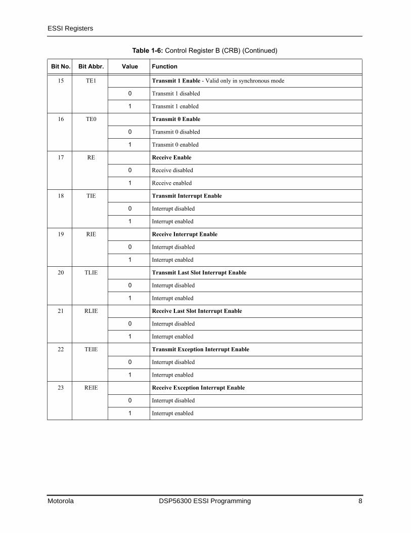
Motorola DSP56300 ESSI Programming 8
ESSI Registers
15 TE1 Transmit 1 Enable - Valid only in synchronous mode
0 Transmit 1 disabled
1 Transmit 1 enabled
16 TE0 Transmit 0 Enable
0 Transmit 0 disabled
1 Transmit 0 enabled
17 RE Receive Enable
0 Receive disabled
1 Receive enabled
18 TIE Transmit Interrupt Enable
0 Interrupt disabled
1 Interrupt enabled
19 RIE Receive Interrupt Enable
0 Interrupt disabled
1 Interrupt enabled
20 TLIE Transmit Last Slot Interrupt Enable
0 Interrupt disabled
1 Interrupt enabled
21 RLIE Receive Last Slot Interrupt Enable
0 Interrupt disabled
1 Interrupt enabled
22 TEIE Transmit Exception Interrupt Enable
0 Interrupt disabled
1 Interrupt enabled
23 REIE Receive Exception Interrupt Enable
0 Interrupt disabled
1 Interrupt enabled
Table 1-6: Control Register B (CRB) (Continued)
Bit No. Bit Abbr. Value Function
ESSI Registers
Motorola ESSI Architecture 9
In addition to the ESSI registers, the three following port registers control ESSI GPIO functionality. Port C is ESSI0 and Port D is ESSI1.
¥ Port Control Register (PCRC & PCRD) Ñ Control the functionality of the ESSI GPIO signals. Each of the five bits in the port control registers controls the functionality of the corresponding port signal pin. When a bit is set, the corresponding port signal is configured as an ESSI signal. When a bit is clear, the corresponding port signal is configured as a GPIO signal.
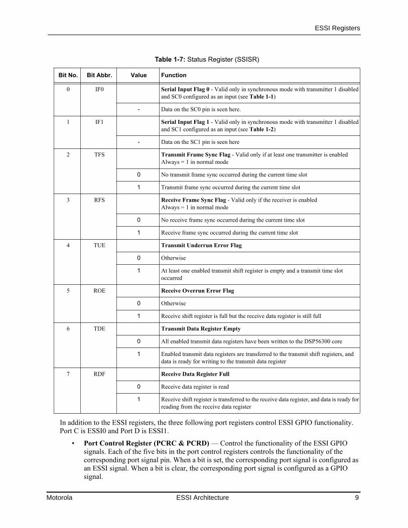
Table 1-7: Status Register (SSISR)
Bit No. Bit Abbr. Value Function
0 IF0 Serial Input Flag 0 - Valid only in synchronous mode with transmitter 1 disabled and SC0 configured as an input (see Table 1-1)
- Data on the SC0 pin is seen here.
1 IF1 Serial Input Flag 1 - Valid only in synchronous mode with transmitter 1 disabled and SC1 configured as an input (see Table 1-2)
- Data on the SC1 pin is seen here
2 TFS Transmit Frame Sync Flag - Valid only if at least one transmitter is enabled Always = 1 in normal mode
0 No transmit frame sync occurred during the current time slot
1 Transmit frame sync occurred during the current time slot
3 RFS Receive Frame Sync Flag - Valid only if the receiver is enabledAlways = 1 in normal mode
0 No receive frame sync occurred during the current time slot
1 Receive frame sync occurred during the current time slot
4 TUE Transmit Underrun Error Flag
0 Otherwise
1 At least one enabled transmit shift register is empty and a transmit time slot occurred
5 ROE Receive Overrun Error Flag
0 Otherwise
1 Receive shift register is full but the receive data register is still full
6 TDE Transmit Data Register Empty
0 All enabled transmit data registers have been written to the DSP56300 core
1 Enabled transmit data registers are transferred to the transmit shift registers, and data is ready for writing to the transmit data register
7 RDF Receive Data Register Full
0 Receive data register is read
1 Receive shift register is transferred to the receive data register, and data is ready for reading from the receive data register
Motorola DSP56300 ESSI Programming 10
ESSI Registers
¥ Port Direction Register (PRRC & PRRD) - Control the direction of the ESSI GPIO signals. Each of the five bits in the port direction registers controls the direction of the corresponding port signal pin if the pin is configured as a GPIO signal. When a bit is set, the corresponding port signal is configured as an output. When a bit is clear, the corresponding port signal is configured as an input.
¥ Port Data Register (PDRC & PDRD) - Read/write data to/from the ESSI GPIO signals. If a port signal is configured as a GPIO input, the corresponding bit reflects the value present on the pin. If a port signal is configured as a GPIO output, the value written into the corresponding bit is reflected on the pin.
Transfer Characteristics
Motorola DSP56300 ESSI Programming 11
Part 2 ESSI Programming
This section describes the practical operation of the ESSI, covering transfer characteristics, synchronization signals, operation modes, initialization method, and transfer methods. In some cases, segments of code illustrate practical programming guidelines. The code in this section uses equate labels for the location of the ESSI registers. These labels include the register name preceded with ÒM_Ó and can be found in the
ioequ.asm
file.
2.1 Transfer Characteristics
Words transferred by the ESSI are characterized by word length, shift direction, and word alignment. This section describes these characteristics and the programming associated with them.
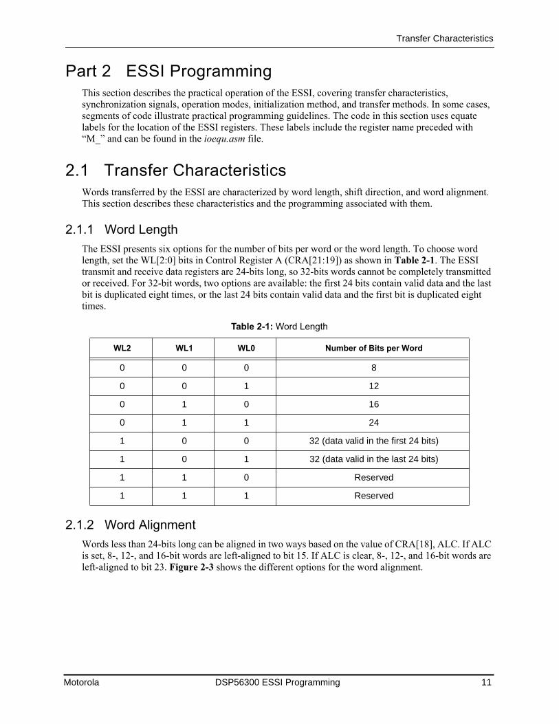
2.1.1 Word Length
The ESSI presents six options for the number of bits per word or the word length. To choose word length, set the WL[2:0] bits in Control Register A (CRA[21:19]) as shown in
Table 2-1
. The ESSI transmit and receive data registers are 24-bits long, so 32-bits words cannot be completely transmitted or received. For 32-bit words, two options are available: the first 24 bits contain valid data and the last bit is duplicated eight times, or the last 24 bits contain valid data and the first bit is duplicated eight times.
2.1.2 Word Alignment
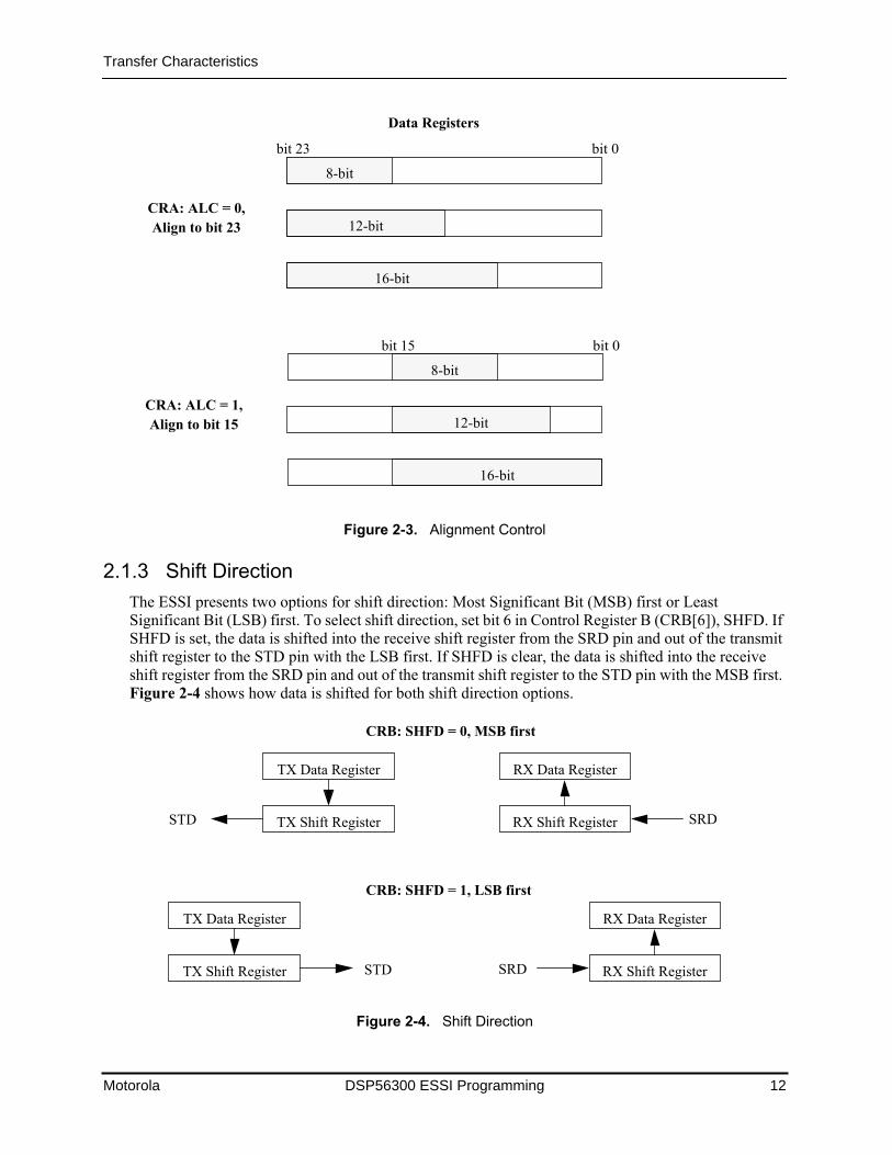
Words less than 24-bits long can be aligned in two ways based on the value of CRA[18], ALC. If ALC is set, 8-, 12-, and 16-bit words are left-aligned to bit 15. If ALC is clear, 8-, 12-, and 16-bit words are left-aligned to bit 23.
Figure 2-3
shows the different options for the word alignment.
Table 2-1:
Word Length
WL2 WL1 WL0 Number of Bits per Word
0 0 0 8
0 0 1 12
0 1 0 16
0 1 1 24
1 0 0 32 (data valid in the first 24 bits)
1 0 1 32 (data valid in the last 24 bits)
1 1 0 Reserved
1 1 1 Reserved
Motorola DSP56300 ESSI Programming 12
Transfer Characteristics
Figure 2-3.
Alignment Control
2.1.3 Shift Direction
The ESSI presents two options for shift direction: Most Significant Bit (MSB) first or Least Significant Bit (LSB) first. To select shift direction, set bit 6 in Control Register B (CRB[6]), SHFD. If SHFD is set, the data is shifted into the receive shift register from the SRD pin and out of the transmit shift register to the STD pin with the LSB first. If SHFD is clear, the data is shifted into the receive shift register from the SRD pin and out of the transmit shift register to the STD pin with the MSB first.
Figure 2-4
shows how data is shifted for both shift direction options.
Figure 2-4.
Shift Direction
12-bit
16-bit
8-bit
CRA: ALC = 0,
bit 0bit 23
12-bit
16-bit
8-bit
CRA: ALC = 1,
bit 0bit 15
Data Registers
Align to bit 23
Align to bit 15
RX Shift RegisterTX Shift Register
RX Shift RegisterTX Shift Register
SRDSTD
SRDSTD
RX Data RegisterTX Data Register
RX Data RegisterTX Data Register
CRB: SHFD = 0, MSB first
CRB: SHFD = 1, LSB first
Synchronization Signals
Motorola DSP56300 ESSI Programming 13
2.2 Synchronization Signals
Because the ESSI is a synchronous interface, it requires clock and frame sync signals to define when the data changes and when a new frame begins. In certain modes, the ESSI also has the option of two flag signals to use for device selection. This section describes all of these signals.
2.2.1 Synchronous Versus Asynchronous
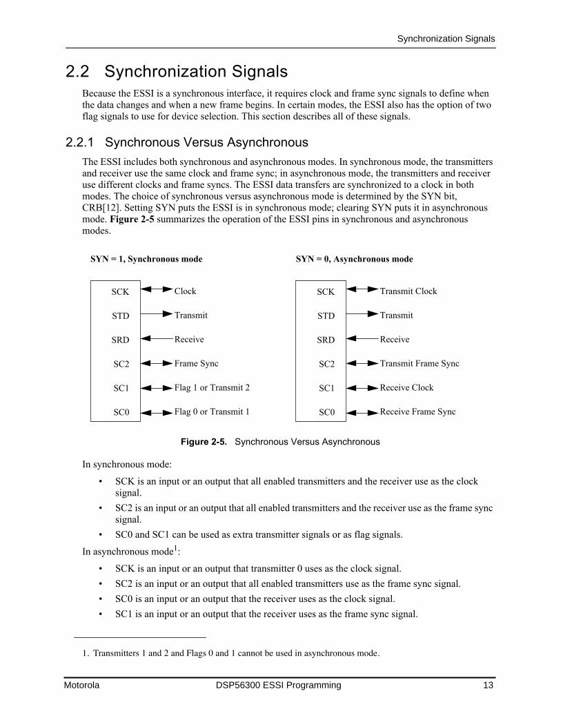
The ESSI includes both synchronous and asynchronous modes. In synchronous mode, the transmitters and receiver use the same clock and frame sync; in asynchronous mode, the transmitters and receiver use different clocks and frame syncs. The ESSI data transfers are synchronized to a clock in both modes. The choice of synchronous versus asynchronous mode is determined by the SYN bit, CRB[12]. Setting SYN puts the ESSI is in synchronous mode; clearing SYN puts it in asynchronous mode.
Figure 2-5
summarizes the operation of the ESSI pins in synchronous and asynchronous modes.
Figure 2-5.
Synchronous Versus Asynchronous
In synchronous mode:
¥ SCK is an input or an output that all enabled transmitters and the receiver use as the clock signal.
¥ SC2 is an input or an output that all enabled transmitters and the receiver use as the frame sync signal.
¥ SC0 and SC1 can be used as extra transmitter signals or as flag signals.
In asynchronous mode
1
:
¥ SCK is an input or an output that transmitter 0 uses as the clock signal.
¥ SC2 is an input or an output that all enabled transmitters use as the frame sync signal.
¥ SC0 is an input or an output that the receiver uses as the clock signal.
¥ SC1 is an input or an output that the receiver uses as the frame sync signal.
1. Transmitters 1 and 2 and Flags 0 and 1 cannot be used in asynchronous mode.
SCK
STD
SRD
SC2
SC1
SC0
Clock
Transmit
Receive
Frame Sync
Flag 1 or Transmit 2
Flag 0 or Transmit 1
SYN = 1, Synchronous mode
SCK
STD
SRD
SC2
SC1
SC0
Transmit Clock
Transmit
Receive
Transmit Frame Sync
Receive Clock
Receive Frame Sync
SYN = 0, Asynchronous mode
Motorola DSP56300 ESSI Programming 14
Synchronization Signals
The direction of the SC0, SC1, SC2, and SCK pins is determined by the SCD0, SCD1, SCD2, and SCKD bits, respectively, CRB[2:5]. If one of these bits is clear, the corresponding pin is an input. If one of these bits is set, the corresponding pin is an output.
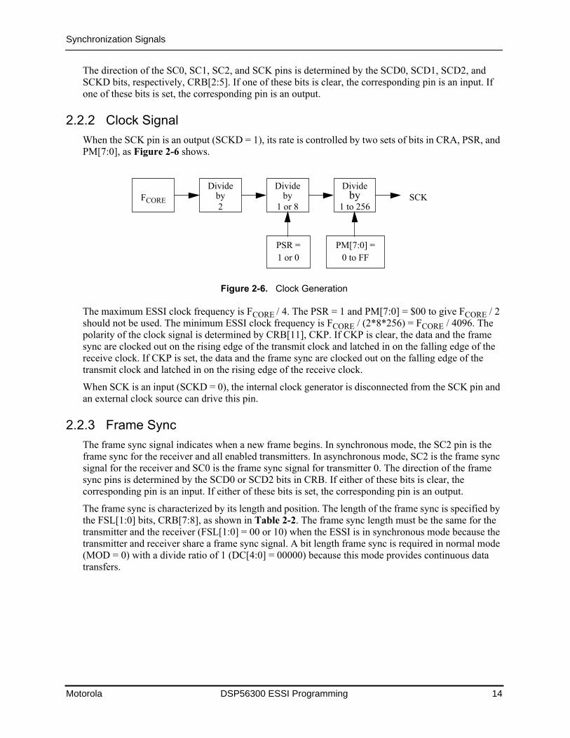
2.2.2 Clock Signal
When the SCK pin is an output (SCKD = 1), its rate is controlled by two sets of bits in CRA, PSR, and PM[7:0], as
Figure 2-6
shows.
Figure 2-6.
Clock Generation
The maximum ESSI clock frequency is F
CORE
/ 4. The PSR = 1 and PM[7:0] = $00 to give F
CORE
/ 2 should not be used. The minimum ESSI clock frequency is F
CORE
/ (2*8*256) = F
CORE
/ 4096. The polarity of the clock signal is determined by CRB[11], CKP. If CKP is clear, the data and the frame sync are clocked out on the rising edge of the transmit clock and latched in on the falling edge of the receive clock. If CKP is set, the data and the frame sync are clocked out on the falling edge of the transmit clock and latched in on the rising edge of the receive clock.
When SCK is an input (SCKD = 0), the internal clock generator is disconnected from the SCK pin and an external clock source can drive this pin.
2.2.3 Frame Sync
The frame sync signal indicates when a new frame begins. In synchronous mode, the SC2 pin is the frame sync for the receiver and all enabled transmitters. In asynchronous mode, SC2 is the frame sync signal for the receiver and SC0 is the frame sync signal for transmitter 0. The direction of the frame sync pins is determined by the SCD0 or SCD2 bits in CRB. If either of these bits is clear, the corresponding pin is an input. If either of these bits is set, the corresponding pin is an output.
The frame sync is characterized by its length and position. The length of the frame sync is specified by the FSL[1:0] bits, CRB[7:8], as shown in
Table 2-2
. The frame sync length must be the same for the transmitter and the receiver (FSL[1:0] = 00 or 10) when the ESSI is in synchronous mode because the transmitter and receiver share a frame sync signal. A bit length frame sync is required in normal mode (MOD = 0) with a divide ratio of 1 (DC[4:0] = 00000) because this mode provides continuous data transfers.
FCORE
Divideby2
Divideby
1 or 8
Divideby
1 to 256
PM[7:0] =PSR =
SCK
1 or 0 0 to FF
Operation Modes
Motorola DSP56300 ESSI Programming 15
Word length frame syncs can be positioned two ways based on the value of CRB[9], FSR. If FSR is clear, the word length frame sync occurs together with the first bit of the data word in the first time slot. If FSR is set, the word length frame sync occurs one clock cycle before the first bit in the data word of the first time slot.
The polarity of the frame sync signals is determined by CRB[10], FSP. If FSP is clear, the frame sync is positive, i.e. the frame sync goes high to indicate a frame start. If FSP is set, the frame sync is negative, i.e. the frame sync goes low to indicate a frame start.
2.2.4 Flags
When the ESSI is in synchronous mode and transmitters 1 and 2 are disabled, the SC0 and SC1 pins are available for use as flags. The following rules apply for the flag signals:
If SC0 is an:
¥ input (SCD0 = 0), data on the SC0 pin is seen on SSISR[0], IF0.
¥ output (SCD0 = 1), data written to OF0, CRB[0], is seen on the SC0 pin.
If SC1 is an:
¥ input (SCD1 = 0), data on the SC1 pin is seen on SSISR[1], IF1.
¥ output (SCD1 = 1), data written to OF1, CRB[1], is seen on the SC1 pin.
The flags can change at the beginning of each frame in normal mode and at the beginning of each time slot in network mode.
There is one additional option for the SC1 pin. In synchronous mode with transmitter 2 disabled, the SC1 pin can be programmed as a transmitter 0 active signal. When the TX0 active pin is high, transmitter 0 is active; when this pin is low, transmitter 0 is not active. This signal can enable an external buffer for the transmitter 0 output. This option is selected using CRA[22], SSC1, which is valid only in synchronous mode with transmitter 2 disabled. If SSC1 is clear, SC1 is the flag 0 signal. If SSC1 is set, SC1 is the transmitter 0 active signal.
2.3 Operation Modes
The ESSI has three basic modes of operation: normal, network, and on-demand. The operation mode is selected by the MOD bit, CRB[11]. If MOD is clear, the ESSI is normal mode. If MOD is set, the ESSI is in network mode. Additionally, the on-demand mode is selected if MOD is set and the DC[4:0] bits in CRA are all clear. The following sections describe each of the operation modes.
Table 2-2:
Frame Sync Length
FSL1 FSL0Frame Sync Length
RX TX
0 0 Word Word
0 1 Word Bit
1 0 Bit Bit
1 1 Bit Word
Motorola DSP56300 ESSI Programming 16
Operation Modes
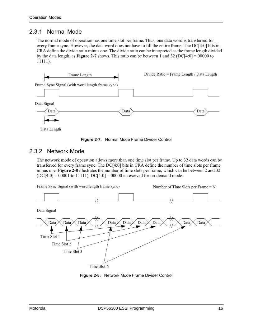
2.3.1 Normal Mode
The normal mode of operation has one time slot per frame. Thus, one data word is transferred for every frame sync. However, the data word does not have to fill the entire frame. The DC[4:0] bits in CRA define the divide ratio minus one. The divide ratio can be interpreted as the frame length divided by the data length, as
Figure 2-7
shows. This ratio can be between 1 and 32 (DC[4:0] = 00000 to 11111).
Figure 2-7.
Normal Mode Frame Divider Control
2.3.2 Network Mode
The network mode of operation allows more than one time slot per frame. Up to 32 data words can be transferred for every frame sync. The DC[4:0] bits in CRA define the number of time slots per frame minus one.
Figure 2-8
illustrates the number of time slots per frame, which can be between 2 and 32 (DC[4:0] = 00001 to 11111). DC[4:0] = 00000 is reserved for on-demand mode.
Figure 2-8.
Network Mode Frame Divider Control
Data Data Data
Frame Sync Signal (with word length frame sync)
Data Signal
Frame Length
Data Length
Divide Ratio = Frame Length / Data Length
Frame Sync Signal (with word length frame sync)
Data Signal
Data Data Data Data Data Data Data Data Data
Time Slot 1
Time Slot 2
Time Slot 3
Time Slot N
Number of Time Slots per Frame = N
Operation Modes
Motorola DSP56300 ESSI Programming 17
Some applications do not require data to be transmitted or received during every time slot. There are two types of registers that control which time slots receive and transmit data: the time slot register and the slot mask registers.
2.3.2.1 Time Slot Register
The time slot register (TSR) is a write-only null data register that prevents data transmission in the current time slot. TSR is similar to a transmit data register. However, when data is written to the TSR, the data is not transmitted. Instead, all of the enabled transmitters are in the high-impedance state for the current time slot. The following code writes an arbitrary data word to the time slot registers for ESSI0 and ESSI1 to disable transmission during the current time slot:
movep #data,x:M_TSR0 ;Write data to ESSI0 TSR0 reg - disable TXmovep #data,x:M_TSR1 ;Write data to ESSI0 TSR1 reg - disable TX
2.3.2.2 Transmit Slot Mask Registers
There are two transmit slot mask registers, Transmit Slot Mask Register A (TSMA) and Transmit Slot Mask Register B (TSMB). Both TSMA and TSMB are 16 bits wide. Together they can be regarded as one 32-bit register, TSM. When bit
n
of the TSM is set, the transmit sequence proceeds normally during time slot
n
. When bit n of the TSM is cleared, the transmit data pins of the enabled transmitters are tri-stated during time slot
n
. Also, when bit
n
of TSM is cleared, the TDE and TUE flags in the SSISR are not set during time slot
n
. Thus, transmit interrupts are generated only for enabled time slots. The transmit slot mask registers do not conflict with the TSR register. Even if a time slot is enabled in the transmit slot mask registers, writing to the TSR disables the transmitters.
The following code writes to the transmit slot mask registers for ESSI0 and ESSI1 to disable transmission during all except the first and the fourth time slots. To ensure that this code runs properly, verify that the DC[4:0] bits are set so that there are at least four time slots per frame.
movep #0009,x:M_TSMA0 ;Load TSMA for ESSI0movep #0000,x:M_TSMB0 ;Load TSMB for ESSI0movep #0009,x:M_TSMA1 ;Load TSMA for ESSI1movep #0000,x:M_TSMB1 ;Load TSMB for ESSI1
2.3.2.3 Receive Slot Mask Registers
There are two receive slot mask registers, Receive Slot Mask Register A (RSMA) and Receive Slot Mask Register B (RSMB). Both RSMA and RSMB are 16 bits wide. Together they can be regarded as one 32-bit register, RSM. When bit
n
of RSM is set, the transmit sequence proceeds normally during time slot
n
. When bit
n
of RSM is cleared, the receive data pins of the enabled transmitters are tri-stated during time slot
n
. Also, when bit
n
of RSM is cleared, the RDF and ROE flags in the SSISR are not set during time slot
n
. Thus, receive interrupts are generated only for enabled time slots.
The following code writes to the receive slot mask registers so that ESSI0 receives only during the first time slot and ESSI1 receives only during the fourth time slot. To ensure that this code runs properly, verify that the DC[4:0] bits are set so that there are at least four time slots per frame.
Motorola DSP56300 ESSI Programming 18
Programming Control Registers
movep #0001,x:M_RSMA0 ;Load RSMA for ESSI0movep #0000,x:M_RSMB0 ;Load RSMB for ESSI0movep #0008,x:M_RSMA1 ;Load RSMA for ESSI1movep #0000,x:M_RSMB1 ;Load RSMB for ESSI1
2.3.2.4 On-Demand Mode
The on-demand mode of operation does not generate a periodic frame sync. Thus, no time slots are defined in this mode. A frame sync is generated only when data is ready to be transmitted, i.e. data is written to a transmit data register. The on-demand mode is selected if the MOD bit is set and the DC[4:0] bits in CRA are all clear. This mode requires that the transmit frame sync be internal (output) and the receive frame sync be external (input) for proper operation. Because the transmit and receive frame syncs must be opposite, only simplex operation (receive or transmit but not both) is allowed in synchronous mode. Duplex operation (receive and transmit simultaneously) is allowed only in asynchronous mode. Transmit underruns are impossible in on-demand mode because there are no transmit time slots. Thus transmit underruns are disabled.
2.4 Programming Control Registers
This section shows how to program the control registers, CRA and CRB, to achieve the characteristics described in previous sections of this document. Two examples are presented, including pinout diagrams and equates describing the control register settings.
2.4.1 Example 1
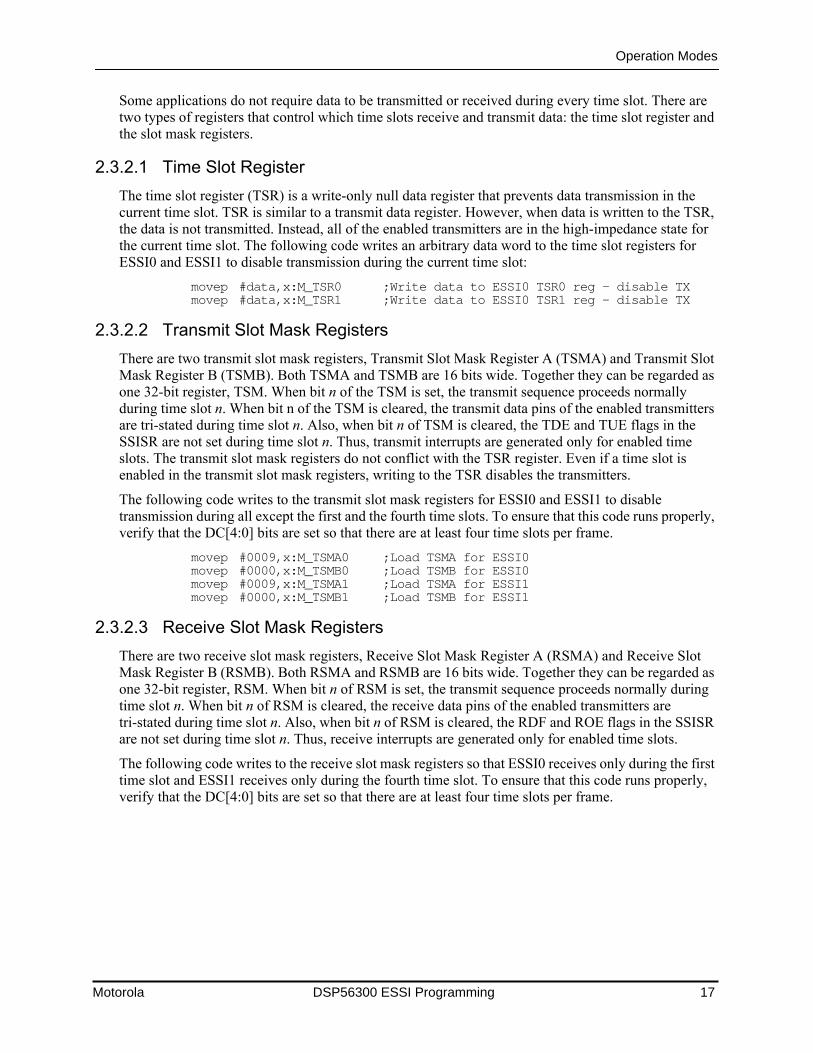
This example programs ESSI0 for normal asynchronous mode.
Figure 2-9
shows the basic pinout diagram for this example. Recall that in asynchronous mode there are separate clock and frame sync signals for the transmit and receive transfers. The comments following the equates describe the other characteristics for this example.
Figure 2-9.
Normal Asynchronous Mode Example
The following code sets up the equates for CRA and CRB, which initialize the ESSI.
STD0
SCK0
SC02
SRD0
SC00
SC01
TX Frame Sync
RX Frame Sync
RX Clock
TX Data
TX Clock
RX Data
Programming Control Registers
Motorola DSP56300 ESSI Programming 19
;-------------------------------------------------------------------------------CRA0 EQU $01F801; ESSI0 Control Register A, CRA; Bit 22 SSC1 0 SC1 pin = serial I/O flag; Bit 21-19 WL[2:0] 000 8 bits/word; Bit 18 ALC 0 Left align to bit 23; Bit 16-12 DC[4:0] 11111 Divide ratio = 32; Bit 11 PSR 1 Fixed prescaler bypassed; Bit 7-0 PM[7:0] 00000001 Clock divide = 2;-------------------------------------------------------------------------------CRB0 EQU $C80DCC; ESSI0 Control Register B, CRB; Bit 23 REIE 1 RX exception int enabled; Bit 22 TEIE 1 TX exception int enabled; Bit 21 RLIE 0 RX last slot int disabled; Bit 20 TLIE 0 TX last slot int disabled; Bit 19 RIE 1 RX int enabled; Bit 18 TIE 0 TX int disabled; Bit 17 RE 0 RX disabled; Bit 16 TE0 0 TX0 disabled; Bit 15 TE1 0 TX1 disabled; Bit 14 TE2 0 TX2 disabled; Bit 13 MOD 0 Normal mode; Bit 12 SYN 0 Asynchronous mode ; Bit 11 CKP 1 Clk polarity on falling edge; Bit 10 FSP 1 Frame sync polarity negative; Bit 9 FSR 0 Frame sync with 1st bit; Bit 8-7 FSL 11 Word length TX frame sync; Bit length RX frame sync; Bit 6 SHFD 1 Shift LSB first ; Bit 5 SCKD 0 External clock source ; Bit 4 SCD2 0 SC2 pin = input ; Bit 3 SCD1 1 SC1 pin = output ; Bit 2 SCD0 1 SC0 pin = output ; Bit 1-0 OF[1:0] 00 Output flags
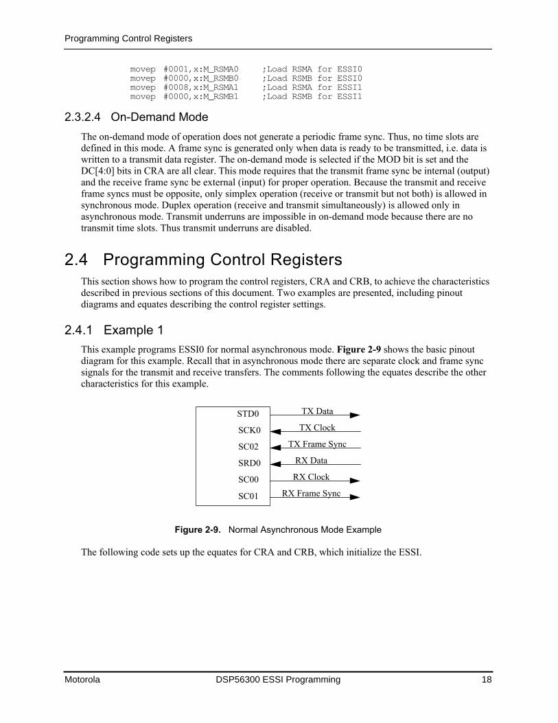
2.4.2 Example 2
This example programs ESSI1 for network synchronous mode.
Figure 2-10
shows the basic pinout diagram for this example. SC11 is the TX0 active signal. The comments following the equates describe the other characteristics for this example.
Figure 2-10.
Network Synchronous Mode Example
The following code sets up the equates for CRA and CRB, which initialize the ESSI.
STD1
SCK1
SC12
SRD1
SC10
SC11
Frame Sync
TX0 Active
Flag 0
TX Data
Clock
RX Data
Motorola DSP56300 ESSI Programming 20
Initialization
CRA1 EQU $505803; ESSI1 Control Register A, CRA; Bit 22 SSC1 1 SC1 pin = TX0 active; Bit 21-19 WL[2:0] 010 16 bits/word; Bit 18 ALC 0 Left align to bit 23; Bit 16-12 DC[4:0] 00101 Number of time slots = 6; Bit 11 PSR 1 Fixed prescaler bypassed; Bit 7-0 PM[7:0] 00000011 Clock divide = 4;-------------------------------------------------------------------------------CRB1 EQU $FC357C; ESSI1 Control Register B, CRB; Bit 23 REIE 1 RX exception int enabled; Bit 22 TEIE 1 TX exception int enabled; Bit 21 RLIE 1 RX last slot int enabled; Bit 20 TLIE 1 TX last slot int enabled; Bit 19 RIE 1 RX int enabled; Bit 18 TIE 1 TX int enabled; Bit 17 RE 0 RX disabled; Bit 16 TE0 0 TX0 disabled; Bit 15 TE1 0 TX1 disabled; Bit 14 TE2 0 TX2 disabled; Bit 13 MOD 1 Network mode; Bit 12 SYN 1 Synchronous mode; Bit 11 CKP 0 Clk polarity on rising edge; Bit 10 FSP 1 Frame sync polarity negative; Bit 9 FSR 0 Frame sync with 1st bit; Bit 8-7 FSL 10 Bit length frame sync; Bit 6 SHFD 1 Shift LSB first; Bit 5 SCKD 1 Internal clock source ; Bit 4 SCD2 1 SC2 pin = output ; Bit 3 SCD1 1 SC1 pin = output ; Bit 2 SCD0 1 SC0 pin = output ; Bit 1-0 OF[1:0] 00 Output flags
2.5 Initialization
Perform the following steps to initialize the ESSI properly:
1. Reset the ESSI.
This is accomplished by a hardware or software reset or by putting the ESSI into its individual reset state by clearing the PCR bits as shown here.
movep #$0,x:M_PCRC ;Reset ESSI0movep #$0,x:M_PCRD ;Reset ESSI1
2. Program the ESSI control registers.
CRA and CRB must be programmed to control the ESSI operation. The following commands program the ESSI control registers by moving equates into CRA and CRB for both ESSIs.
movep #CRA0,x:M_CRA0 ;Load CRA for ESSI0movep #CRB0,x:M_CRB0 ;Load CRB for ESSI0movep #CRA1,x:M_CRA1 ;Load CRA for ESSI1movep #CRB1,x:M_CRB1 ;Load CRB for ESSI1
3. Enable the ESSI pins.
Set the bits in the PCRC and PCRD registers that correspond to the ESSI pins to be used. The following commands set all of the Port C and Port D bits to enable all the ESSI0 and ESSI1 pins.
Transfer Methods
Motorola DSP56300 ESSI Programming 21
movep #$3F,x:M_PCRC ;Enable ESSI0movep #$3F,x:M_PCRD ;Enable ESSI1
4. Write the Þrst data to the transmit registers.
The first data word to be transmitted should be present in the transmit data registers before the transmitters are enabled (even if DMA is used to transfer data to the transmit register). The following commands write the first data to all the transmit data registers for both ESSIs.
TX*_data1
represents any register or memory location that contains the first data to be transmitted.
movep TX00_data1,x:M_TX00 ;Write first data to ESSI0 TX0 regmovep TX01_data1,x:M_TX01 ;Write first data to ESSI0 TX1 regmovep TX02_data1,x:M_TX02 ;Write first data to ESSI0 TX2 regmovep TX10_data1,x:M_TX10 ;Write first data to ESSI1 TX0 regmovep TX11_data1,x:M_TX11 ;Write first data to ESSI1 TX1 regmovep TX12_data1,x:M_TX12 ;Write first data to ESSI1 TX2 reg
5. Enable the transmitters and receiver.
Set the transmitter and receiver enable bits in CRB0 and CRB1 as follows.
bset #14,x:M_CRB0 ;Enable ESSI0 TX2bset #15,x:M_CRB0 ;Enable ESSI0 TX1bset #16,x:M_CRB0 ;Enable ESSI0 TX0bset #14,x:M_CRB1 ;Enable ESSI1 TX2bset #15,x:M_CRB1 ;Enable ESSI1 TX1bset #16,x:M_CRB1 ;Enable ESSI1 TX0bset #17,x:M_CRB0 ;Enable ESSI0 REbset #17,x:M_CRB1 ;Enable ESSI1 RE
2.6 Transfer Methods
The ESSI provides three methods for transferring data to or from the data registers: polling, interrupts, and DMA. Polling is the easiest method, but it demands a large amount of the DSP56300 coreÕs processing power. The DSP56300 core cannot be involved in other processing activities while it polls the receive and transmit ready bits. Interrupts, on the other hand, require more code, but the Core can process other routines while waiting for the ESSI transfers. DMA requires even less core intervention and the setup code is minimal, but the DMA channels must be available. The following sections describe each transfer method.
2.6.1 Polling
The SSISR provides bits that notify the core when data is ready to be transferred to or from the ESSI. The core can poll these bits to determine when to interact with the ESSI. For proper operation, the DSP core must write to the transmit buffer only when it is empty and read from the receive data register when it is full.
SSISR[6], Transmit Data Register Empty (TDE), determines when to write to the transmit data registers. TDE is cleared when the core writes to all enabled transmit data registers. TDE is set when this data is transferred from the transmit data registers into the transmit shift registers. Thus, when TDE is set, the transmit data registers are empty and the core can write to the transmit data registers. The following code polls the TDE bit and writes to the transmit registers when this bit is set.
TX*_data
represents any register or memory location that contains the data to be transmitted.
Motorola DSP56300 ESSI Programming 22
Transfer Methods
jclr #6,x:M_SSISR0,* ;Wait until ESSI0 transmit registers are emptymovep TX00_data,x:M_TX00 ;Write data to ESSI0 TX0 regmovep TX01_data,x:M_TX01 ;Write data to ESSI0 TX1 regmovep TX02_data,x:M_TX02 ;Write data to ESSI0 TX2 reg
jclr #6,x:M_SSISR1,* ;Wait until ESSI1 transmit registers are emptymovep TX10_data,x:M_TX10 ;Write data to ESSI1 TX0 regmovep TX11_data,x:M_TX11 ;Write data to ESSI1 TX1 regmovep TX12_data,x:M_TX12 ;Write data to ESSI1 TX2 reg
SSISR[7], Receive Data Register Full (RDF), determines when to read from the receive data register. RDF is cleared when the core reads data from the receive data register. RDF is set when data is transferred from the receive shift register to the receive data register. Thus, when RDF is set, the receive data register is full and the core can read from the receive data register. The following code polls the RDF bit and reads from the receive register when this bit is set. RX*_data represents any register or memory location to which received data should be written.
jclr #7,x:M_SSISR0,* ;Wait until ESSI0 receive register is fullmovep x:M_RX0,RX0_data ;Read data from ESSI0 RX reg
jclr #7,x:M_SSISR1,* ;Wait until ESSI1 receive register is fullmovep x:M_RX1,RX1_data ;Read data from ESSI1 RX reg
2.6.2 Interrupts
The ESSI provides the following six interrupts, which are listed from highest to lowest priority:
¥ Receive Data with Exception
Ñ Enabled by setting CRB[23], REIE.
Ñ Triggered when ROE (a receiver overrun error is detected), RDF (the receive data register is full) and REIE are set simultaneously.
Ñ Cleared by reading from SSISR and then from RX.
¥ Receive Data
Ñ Enabled by setting CRB[19], RIE.
Ñ Triggered when RDF (the receive data register is full) and RIE are set simultaneously.
Ñ Cleared by reading from RX.
¥ Receive Last Slot
Ñ Enabled by setting CRB[21], RLIE.
Ñ Triggered in network mode when RLIE is set and the last time slot ends.
Ñ Maximum time to service this interrupt must be less than the time to service the number of bits in one time slot.
¥ Transmit Data with Exception
Ñ Enabled by setting CRB[22], TEIE.
Ñ Triggered when TUE (a transmit underrun error has been detected), TDE (the transmit data register is empty) and TEIE are set simultaneously.
Ñ Cleared by writing to SSISR and then by writing to all enabled TX registers or to TSR.
Transfer Methods
Motorola DSP56300 ESSI Programming 23
¥ Transmit Last Slot
Ñ Enabled by setting CRB[20], TLIE.
Ñ Triggered in network mode when TLIE is set and the last time slot is beginning.
Ñ Maximum time to service this interrupt must be less than the time to service the number of bits in one time slot.
¥ Transmit Data
Ñ Enabled by setting CRB[18], TIE.
Ñ Triggered when TDE (the transmit data register is empty) and TIE are set simultaneously.
Ñ Cleared by writing to all enabled TX registers or to TSR.
Configuring interrupts requires two steps: setting up the interrupt routine and enabling the interrupts. To set up the interrupt routine, place the code to be run during the interrupt at the interrupt starting address. The interrupt routines can be short (only two opcodes long) or long (more that two opcodes that requires a jsr instruction). Enabling the interrupts involves setting the corresponding bits in CRB and enabling the ESSI interrupts in the Interrupt Priority Register - Peripheral (IPRP) and enabling global interrupts in the Mode Register (MR) portion of the Status Register (SR).
The following code sets up short interrupt routines to service the ESSI0 and ESSI1 transmitter 0 and receiver. This code uses equate labels for the location of the ESSI interrupt starting addresses. These labels include the interrupt name preceded with ÒI_Ó and can be found in the intequ.asm file. TX*_data represents any register or memory location that contains the data to be transmitted and RX*_data represents any register or memory location to which received data should be written.
org p:I_SI0TDmovep TX00_data,x:M_TX00 ;Write data to ESSI0 TX0 reg
org p:I_SI1TDmovep TX10_data,x:M_TX10 ;Write data to ESSI1 TX0 reg
org p:I_SI0RDmovep x:M_RX0,RX0_data ;Read data from ESSI0 RX reg
org p:I_SI1RDmovep x:M_RX1,RX1_data ;Read data from ESSI1 RX reg
The following code enables the ESSI0 and ESSI1 transmit and receive interrupts. Instead of the first four commands, the interrupt enable bits in CRB can alternatively be set when CRB is initially programmed (as in Step 2 of Section 2.5).
bset #18,x:M_CRB0 ;Enable ESSI0 transmit interruptbset #19,x:M_CRB0 ;Enable ESSI0 receive interruptbset #18,x:M_CRB1 ;Enable ESSI1 transmit interruptbset #19,x:M_CRB1 ;Enable ESSI1 receive interruptandi $FC,mr ;Unmask interruptsmovep #$03C,x:M_IPRP ;Set ESSI1 and ESSI0 interrupt to priority 2
2.6.3 DMA
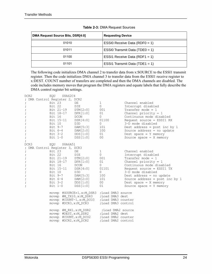
The Direct Memory Access (DMA) controller is an on-chip device that permits data transfers between internal/external memory and/or internal/external I/O in any combination, without intervention of the core. Due to dedicated DMA address and data buses as well as internal memory partitioning, a high level of isolation is achieved so that DMA operation does not interfere with or slow down the core operation. The DMA can move data to the ESSI transmit register and from the ESSI receive register. Table 2-3 shows the four available ESSI DMA request sources. The DMA request source bits are used in the DMA Control Register, DCR[15:11].
Motorola DSP56300 ESSI Programming 24
Transfer Methods
The following code initializes DMA channel 2 to transfer data from x:SOURCE to the ESSI1 transmit register. Then the code initializes DMA channel 3 to transfer data from the ESSI1 receive register to x:DEST. COUNT number of transfers are completed and then the DMA channels are disabled. The code includes memory moves that program the DMA registers and equate labels that fully describe the DMA control register bit settings.
DCR2 EQU $8A62C4; DMA Control Register 2, DCR2; Bit 23 DE 1 Channel enabled; Bit 22 DIE 0 Interrupt disabled; Bit 21-19 DTM[2:0] 001 Transfer mode = 1; Bit 18-17 DPR[1:0] 01 Channel priority = 1; Bit 16 DCON 0 Continuous mode disabled; Bit 15-11 DSR[4:0] 01100 Request source = ESSI1 RX; Bit 10 D3D 0 3-D mode disabled; Bit 9-7 DAM[5:3] 101 Dest address = post inc by 1; Bit 6-4 DAM[2:0] 100 Source address = no update; Bit 3-2 DDS[1:0] 01 Dest space = Y memory; Bit 1-0 DSS[1:0] 00 Source space = X memory;DCR3 EQU $8A6A51; DMA Control Register 3, DCR3; Bit 23 DE 1 Channel enabled; Bit 22 DIE 0 Interrupt disabled; Bit 21-19 DTM[2:0] 001 Transfer mode = 1; Bit 18-17 DPR[1:0] 01 Channel priority = 1; Bit 16 DCON 0 Continuous mode disabled; Bit 15-11 DSR[4:0] 01101 Request source = ESSI1 TX; Bit 10 D3D 0 3-D mode disabled; Bit 9-7 DAM[5:3] 100 Dest address = no update ; Bit 6-4 DAM[2:0] 101 Source address = post inc by 1; Bit 3-2 DDS[1:0] 00 Dest space = X memory; Bit 1-0 DSS[1:0] 01 Source space = Y memory
movep #SOURCE+1,x:M_DSR3 ;Load DMA3 sourcemovep #M_TX10,x:M_DDR3 ;Load DMA3 destmovep #COUNT-1,x:M_DCO3 ;Load DMA3 countermovep #DCR3,x:M_DCR3 ;Load DMA3 control
movep #M_RX1,x:M_DSR2 ;Load DMA2 sourcemovep #DEST,x:M_DDR2 ;Load DMA2 destmovep #COUNT,x:M_DCO2 ;Load DMA2 countermovep #DCR2,x:M_DCR2 ;Load DMA2 control
Table 2-3: DMA Request Sources
DMA Request Source Bits, DSR[4:0] Requesting Device
01010 ESSI0 Receive Data (RDF0 = 1)
01011 ESSI0 Transmit Data (TDE0 = 1)
01100 ESSI1 Receive Data (RDF1 = 1)
01101 ESSI1 Transmit Data (TDE1 = 1)
References
Motorola DSP56300 ESSI Programming 25
2.7 References1. DSP56300 Family Manual, Motorola, 1995. Order this document by the order number
DSP56300FM/AD. Or download it from the Motorola Web site at:http://www.mot.com/SPS/DSP/documentation/DSP56300.html
2. DSP56303 UserÕs Manual, Motorola, 1996. Order this document by the order number DSP56303UM/AD. Or download it from the Motorola Web site at:http://www.mot.com/SPS/DSP/documentation/DSP56300.html
3. Download the equate Þles, ioequ.asm and intequ.asm, from the Motorola Web site at:http://www.mot.com/SPS/DSP/software/other.html
Motorola DSP56300 ESSI Programming 26
References
NOTES:

References
Motorola DSP56300 ESSI Programming 27
NOTES:
Motorola reserves the right to make changes without further notice to any products herein. Motorola makes no warranty, representation or guarantee regarding the suitability of its products for any particular purpose, nor does Motorola assume any liability arising out of the application or use of any product or circuit, and specifically disclaims any and all liability, including without limitation consequential or incidental damages. “Typical” parameters which may be provided in Motorola data sheets and/or specifications can and do vary in different applications and actual performance may vary over time. All operating parameters, including “Typicals” must be validated for each customer application by customer’s technical experts. Motorola does not convey any license under its patent rights nor the rights of others. Motorola products are not designed, intended, or authorized for use as components in systems intended for surgical implant into the body, or other applications intended to support life, or for any other application in which the failure of the Motorola product could create a situation where personal injury or death may occur. Should Buyer purchase or use Motorola products for any such unintended or unauthorized application, Buyer shall indemnify and hold Motorola and its officers, employees, subsidiaries, affiliates, and distributors harmless against all claims, costs, damages, and expenses, and reasonable attorney fees arising out of, directly or indirectly, any claim of personal injury or death associated with such unintended or unauthorized use, even if such claim alleges that Motorola was negligent regarding the design or manufacture of the part. Motorola and are registered trademarks of Motorola, Inc. Motorola, Inc. is an Equal Opportunity/Affirmative Action Employer.
How to reach us:
USA/Europe/Locations Not Listed:Motorola Literature DistributionP.O. Box 5405Denver, Colorado 802171 (800) 441-2447 1 (303) 675-2140
Motorola Fax Back System (Mfax™):TOUCHTONE (602) 244-66091 (800) [email protected]
Asia/Pacific:Motorola Semiconductors H.K. Ltd.8B Tai Ping Industrial Park51 Ting Kok RoadTai Po, N.T., Hong Kong852-26629298
Technical Resource Center:1 (800) 521-6274
Japan:Nippon Motorola LtdSPD, Strategic Planning Office1414-32-1, Nishi-GotandaShinagawa-ku, Japan81-3-5487-8488
Internet:http://www.motorola-dsp.com/
OnCE and Mfax are registered trademarks of Motorola, Inc.