Embed Size (px)
Citation preview
Freescale SemiconductorApplication Note
AN1839Rev. 1, 8/2005
CONTENTS1 OnCE Module .........................................................11.1 OnCE Controller .....................................................21.2 OnCE Memory Breakpoint Logic ...........................41.3 OnCE Trace Logic ..................................................51.4 Pipeline Information and the OGDB Register ........61.5 OnCE Trace Buffer .................................................62 JTAG Port ............................................................... 72.1 TAP Controller ........................................................72.2 Signals .....................................................................92.3 JTAG Instruction Register ......................................92.4 JTAG ID Register .................................................102.5 JTAG Boundary Scan Register .............................103 Serial Protocol .......................................................114 Examples of OnCE/JTAG Interaction ..................114.1 Entering the Test-Logic-Reset State ..................... 124.2 Executing the JTAG DEBUG_REQUEST
Instruction .............................................................144.3 Executing the JTAG ENABLE_ONCE
Instruction .............................................................144.4 Reading the Pipeline Registers .............................154.5 Reading the Trace Buffer ......................................174.6 Writing to Memory ...............................................214.7 Reading from Memory ..........................................24
Programming the DSP56300 OnCE and JTAG PortsBy Barbara Johnson
This application note describes the DSP56300 OnCE and JTAG ports and explains how they interact. A series of examples demonstrates how to use the OnCE and JTAG ports to enter Debug mode, save pipeline registers, read from the trace buffer, write to memory, and read from memory. For more information on the OnCE and JTAG ports, see the applicable sections of the DSP56300 Family Manual.
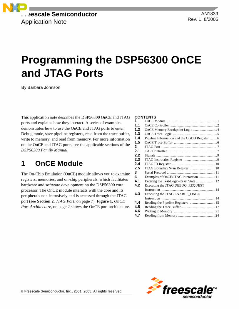
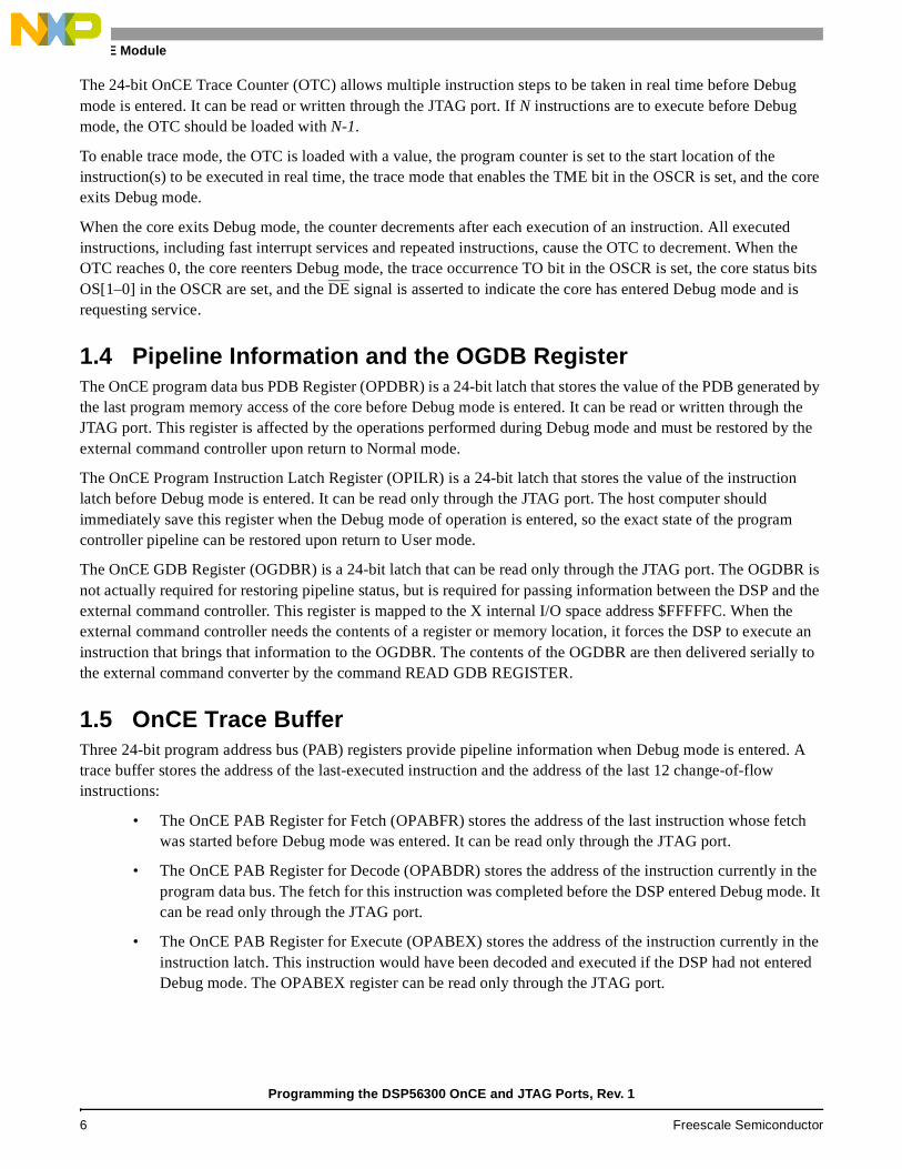
1 OnCE ModuleThe On-Chip Emulation (OnCE) module allows you to examine registers, memories, and on-chip peripherals, which facilitates hardware and software development on the DSP56300 core processor. The OnCE module interacts with the core and its peripherals non-intrusively and is accessed through the JTAG port (see Section 2, JTAG Port, on page 7). Figure 1, OnCE Port Architecture, on page 2 shows the OnCE port architecture.
© Freescale Semiconductor, Inc., 2001, 2005. All rights reserved.
OnCE Module
Figure 1. OnCE Port Architecture
1.1 OnCE ControllerTo communicate with the OnCE controller, the DSP must be in Debug mode. To enter Debug mode from a hardware or software breakpoint, either single step through opcodes or assert the DE pin. A state machine decodes 8-bit commands specified in the OnCE Command Register (OCR) and controls the interaction with the OnCE registers. The OCR receives serial data from the TDI signal.
OPDBR
OPILR
OnCE PIPELINE INFO
OCR
OnCE CONTROLLER
OnCE TRACE LOGIC
OTC
TDI
TCK
TDO
OSCR
OGDBR
OMAL
OMAC0
OnCE BREAKPOINT LOGIC
OMLR0
OMAC1
OMLR1
OBCR
PABXABYAB
OMBC
DE
OnCE TRACE BUFFER
PAB FETCH
PAB DECODE
Trace Buffer Reg 11
CIR
CU
LAR
BU
FF
ER
PO
INT
ER
PAB EXECUTE
Trace Buffer Reg 0
Trace Buffer Shift Reg
PAB
Programming the DSP56300 OnCE and JTAG Ports, Rev. 1
2 Freescale Semiconductor
OnCE Module
The OnCE decoder (ODEC) receives the 8-bit command from the OCR, a signal from the JTAG controller to indicate that it has received 8 or 24 bits and that an update of the selected data register must be performed, and a signal indicating that the core has halted. The 24-bit OnCE Status and Control Register (OSC) enables trace mode and indicates the reason for entering Debug mode.
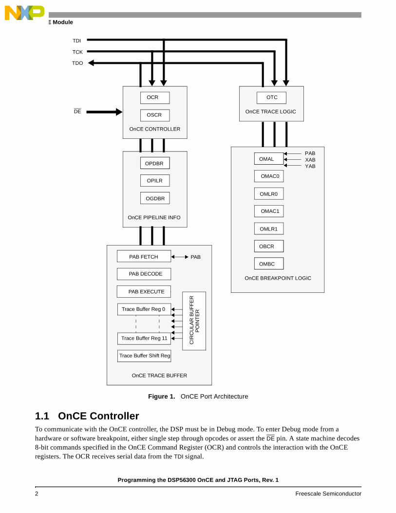
1.1.1 OnCE Command Register (OCR)Table 1 shows the OCR and Table 2 shows the selected OCR registers.
Table 1. OnCE Command Register (OCR) Bits
Bit Name Description
7Read/Write Command
R/W = 0 Writes the data associated with the command into the register specified by RS[4–0].
R/W = 1 Reads the data in the register specified by RS[4–0].
6Go Command
GO = 0 Inactive. No action taken.
GO = 1 Executes the instruction in the OPILR register. See “Pipeline Information and the OGDB Register” on page 6.
5Exit Command
EX = 0 Remains in Debug mode.
EX = 1 Leaves Debug mode and resumes normal operation.
4-0Register Select
RS[4–0] Register select bits that define which register is the source or destination for read or write operations. Refer to Table 2.
Table 2. OCR Register Select Bits
RS[4–0] Register Selected See Also
00000 OnCE Status and Control Register (OSCR). Section 1.1.2, OnCE Status and Control Register (OSCR), on page 4.
00001 Memory Breakpoint Counter (OMBC). Section 1.2, OnCE Memory Breakpoint Logic, on page 4.
00010 Breakpoint Control Register (OBCR). Section 1.2, OnCE Memory Breakpoint Logic, on page 4
00101 Memory Limit Register 0 (OMLR0). Section 1.2, OnCE Memory Breakpoint Logic, on page 4
00110 Memory Limit Register 1 (OMLR1). Section 1.2, OnCE Memory Breakpoint Logic, on page 4
01001 GDB Register (OGDBR). Section 1.4, Pipeline Information and the OGDB Register, on page 6.
01010 PDB Register (OPDBR). Section 1.4, Pipeline Information and the OGDB Register, on page 6.
01011 PIL Register (OPILR). Section 1.4, Pipeline Information and the OGDB Register, on page 6.
01100 PDB GO-TO Register (for GO TO command) N/A
01101 Trace Counter (OTC). See Section 1.3, OnCE Trace Logic, on page 5.
01110 Tags Buffer (TAGB). N/A
01111 PAB Register for Fetch (OPABFR). Section 1.5, OnCE Trace Buffer, on page 6.
10000 PAB Register for Decode (OPABDR). Section 1.5, OnCE Trace Buffer, on page 6.
10001 PAB Register for Execute (OPABEX). Section 1.5, OnCE Trace Buffer, on page 6.
10010 Trace Buffer and Increment Pointer. Section 1.5, OnCE Trace Buffer, on page 6.
11111 No Register Selected N/A
Programming the DSP56300 OnCE and JTAG Ports, Rev. 1
Freescale Semiconductor 3
OnCE Module
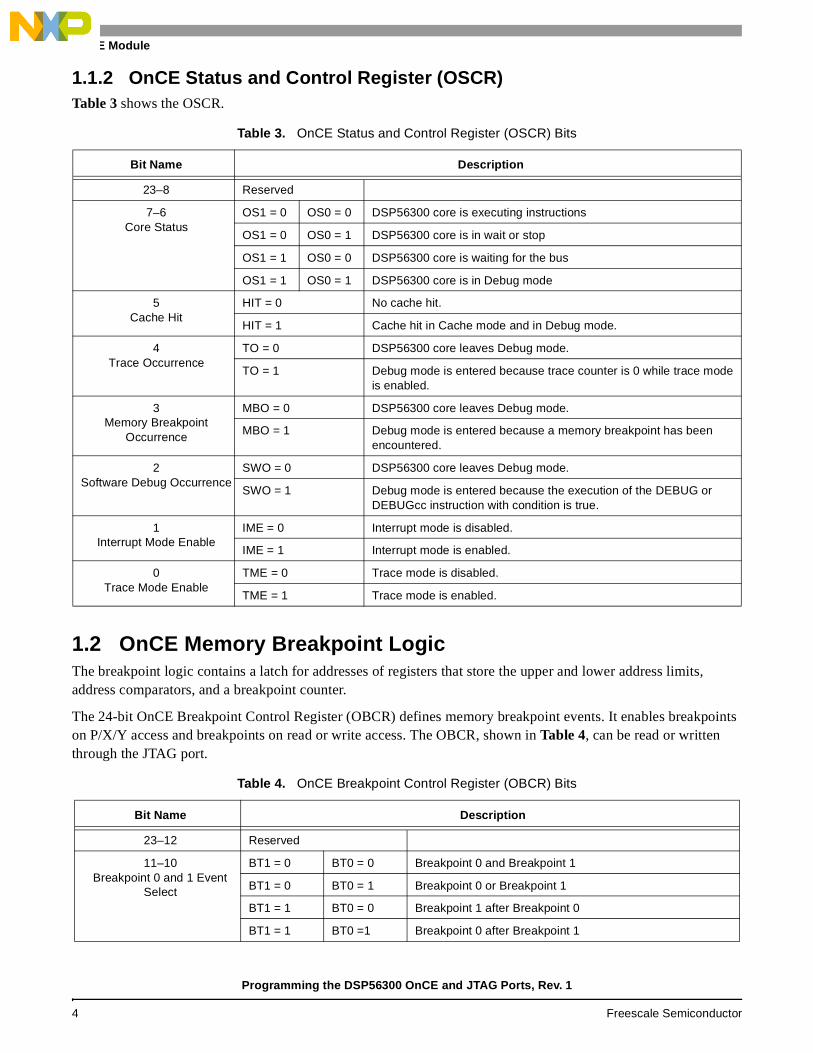
1.1.2 OnCE Status and Control Register (OSCR)Table 3 shows the OSCR.
1.2 OnCE Memory Breakpoint LogicThe breakpoint logic contains a latch for addresses of registers that store the upper and lower address limits, address comparators, and a breakpoint counter.
The 24-bit OnCE Breakpoint Control Register (OBCR) defines memory breakpoint events. It enables breakpoints on P/X/Y access and breakpoints on read or write access. The OBCR, shown in Table 4, can be read or written through the JTAG port.
Table 3. OnCE Status and Control Register (OSCR) Bits
Bit Name Description
23–8 Reserved
7–6Core Status
OS1 = 0 OS0 = 0 DSP56300 core is executing instructions
OS1 = 0 OS0 = 1 DSP56300 core is in wait or stop
OS1 = 1 OS0 = 0 DSP56300 core is waiting for the bus
OS1 = 1 OS0 = 1 DSP56300 core is in Debug mode
5Cache Hit
HIT = 0 No cache hit.
HIT = 1 Cache hit in Cache mode and in Debug mode.
4Trace Occurrence
TO = 0 DSP56300 core leaves Debug mode.
TO = 1 Debug mode is entered because trace counter is 0 while trace mode is enabled.
3Memory Breakpoint
Occurrence
MBO = 0 DSP56300 core leaves Debug mode.
MBO = 1 Debug mode is entered because a memory breakpoint has been encountered.
2Software Debug Occurrence
SWO = 0 DSP56300 core leaves Debug mode.
SWO = 1 Debug mode is entered because the execution of the DEBUG or DEBUGcc instruction with condition is true.
1Interrupt Mode Enable
IME = 0 Interrupt mode is disabled.
IME = 1 Interrupt mode is enabled.
0Trace Mode Enable
TME = 0 Trace mode is disabled.
TME = 1 Trace mode is enabled.
Table 4. OnCE Breakpoint Control Register (OBCR) Bits
Bit Name Description
23–12 Reserved
11–10Breakpoint 0 and 1 Event
Select
BT1 = 0 BT0 = 0 Breakpoint 0 and Breakpoint 1
BT1 = 0 BT0 = 1 Breakpoint 0 or Breakpoint 1
BT1 = 1 BT0 = 0 Breakpoint 1 after Breakpoint 0
BT1 = 1 BT0 =1 Breakpoint 0 after Breakpoint 1
Programming the DSP56300 OnCE and JTAG Ports, Rev. 1
4 Freescale Semiconductor
OnCE Module
The OnCE Memory Limit Register 0 (OMLR0) stores the memory breakpoint 0 limit. The OnCE Memory Limit Register 1 (OMLR1) stores the memory breakpoint 1 limit. Both registers are 24-bit and can be read or written through the JTAG port.
The 24-bit OnCE Memory Address Latch (OMAL) register latches the PAB, XAB, YAB, or DAB on every instruction cycle according to the Memory Breakpoint 0 and 1 Select MBS[1–0] bits in the OBCR. The OnCE Memory Address Comparator 0 (OMAC0) compares the current memory address stored in OMAL with the OMLR0 contents. The OnCE Memory Address Comparator 1 (OMAC1) compares the current memory address stored in OMAL with the OMLR1 contents.
The 24-bit OnCE Memory Breakpoint Counter (OMBC) is loaded with a value equal to the number of times minus one that a memory access event should occur before a memory breakpoint is declared. The OBCR and the memory limit registers specify the memory access event. The breakpoint counter decrements on each occurrence of the memory access event. The DSP enters Debug mode when the counter reaches 0 and a new event occurs. The OMBC can be read or written through the JTAG port.
1.3 OnCE Trace LogicThe OnCE trace logic allows execution of instructions in single or multiple steps. It causes the DSP to enter Debug mode after one or more instructions execute and to wait for OnCE commands from the debug serial port.
9–8Breakpoint 1 Condition
Select
CC11 = 0 CC10 = 0 Breakpoint on not equal
CC11 = 0 CC10 = 1 Breakpoint on equal
CC11 = 1 CC10 = 0 Breakpoint on less than
CC11 = 1 CC10 = 1 Breakpoint on greater than
7–6Breakpoint 1 Read/Write
Select
RW11 = 0 RW10 = 0 Breakpoint disabled
RW11 = 0 RW10 = 1 Breakpoint on write access
RW11 = 1 RW10 = 0 Breakpoint on read access
RW11 = 1 RW10 = 1 Breakpoint on read or write access
5–4Breakpoint 0 Condition
Select
CC01 = 0 CC00 = 0 Breakpoint on not equal
CC01 = 0 CC00 = 1 Breakpoint on equal
CC01 = 1 CC00 = 0 Breakpoint on less than
CC01 = 1 CC00 = 1 Breakpoint on greater than
3–2Breakpoint 0 Read/Write
Select
RW01 = 0 RW00 = 0 Breakpoint disabled
RW01 = 0 RW00 = 1 Breakpoint on write access
RW01 = 1 RW00 = 0 Breakpoint on read access
RW01 = 1 RW00 = 1 Breakpoint on read or write access
1–0Memory Breakpoint 0 and 1
Select
MBS1 = 0 MBS0 = 0 Breakpoint on DMA access
MBS1 = 0 MBS0 = 1 Breakpoint on P access
MBS1 = 1 MBS0 = 0 Breakpoint on X access
MBS1 = 1 MBS0 = 1 Breakpoint on Y access
Table 4. OnCE Breakpoint Control Register (OBCR) Bits
Bit Name Description
Programming the DSP56300 OnCE and JTAG Ports, Rev. 1
Freescale Semiconductor 5
OnCE Module
The 24-bit OnCE Trace Counter (OTC) allows multiple instruction steps to be taken in real time before Debug mode is entered. It can be read or written through the JTAG port. If N instructions are to execute before Debug mode, the OTC should be loaded with N-1.
To enable trace mode, the OTC is loaded with a value, the program counter is set to the start location of the instruction(s) to be executed in real time, the trace mode that enables the TME bit in the OSCR is set, and the core exits Debug mode.
When the core exits Debug mode, the counter decrements after each execution of an instruction. All executed instructions, including fast interrupt services and repeated instructions, cause the OTC to decrement. When the OTC reaches 0, the core reenters Debug mode, the trace occurrence TO bit in the OSCR is set, the core status bits OS[1–0] in the OSCR are set, and the DE signal is asserted to indicate the core has entered Debug mode and is requesting service.
1.4 Pipeline Information and the OGDB RegisterThe OnCE program data bus PDB Register (OPDBR) is a 24-bit latch that stores the value of the PDB generated by the last program memory access of the core before Debug mode is entered. It can be read or written through the JTAG port. This register is affected by the operations performed during Debug mode and must be restored by the external command controller upon return to Normal mode.
The OnCE Program Instruction Latch Register (OPILR) is a 24-bit latch that stores the value of the instruction latch before Debug mode is entered. It can be read only through the JTAG port. The host computer should immediately save this register when the Debug mode of operation is entered, so the exact state of the program controller pipeline can be restored upon return to User mode.
The OnCE GDB Register (OGDBR) is a 24-bit latch that can be read only through the JTAG port. The OGDBR is not actually required for restoring pipeline status, but is required for passing information between the DSP and the external command controller. This register is mapped to the X internal I/O space address $FFFFFC. When the external command controller needs the contents of a register or memory location, it forces the DSP to execute an instruction that brings that information to the OGDBR. The contents of the OGDBR are then delivered serially to the external command converter by the command READ GDB REGISTER.
1.5 OnCE Trace BufferThree 24-bit program address bus (PAB) registers provide pipeline information when Debug mode is entered. A trace buffer stores the address of the last-executed instruction and the address of the last 12 change-of-flow instructions:
• The OnCE PAB Register for Fetch (OPABFR) stores the address of the last instruction whose fetch was started before Debug mode was entered. It can be read only through the JTAG port.
• The OnCE PAB Register for Decode (OPABDR) stores the address of the instruction currently in the program data bus. The fetch for this instruction was completed before the DSP entered Debug mode. It can be read only through the JTAG port.
• The OnCE PAB Register for Execute (OPABEX) stores the address of the instruction currently in the instruction latch. This instruction would have been decoded and executed if the DSP had not entered Debug mode. The OPABEX register can be read only through the JTAG port.
Programming the DSP56300 OnCE and JTAG Ports, Rev. 1
6 Freescale Semiconductor
JTAG Port
The circular trace buffer contains 25-bit registers and a 4-bit counter. Although all 12 of the trace buffer registers have the same address, any read access to the trace buffer address increments the counter, thus pointing to the next trace buffer register.
When the DSP enters Debug mode, the trace buffer counter points to the trace buffer register containing the address of the last executed instructions. The first trace buffer read obtains the oldest address, and the following trace buffer reads obtain the other addresses from the oldest to newest, in order of execution. A complete set of 12 reads of the trace buffer must be performed, since each read increments the trace buffer pointer, thus pointing to the next location. After 12 reads, the pointer indicates the same location as it did before the read procedure started.
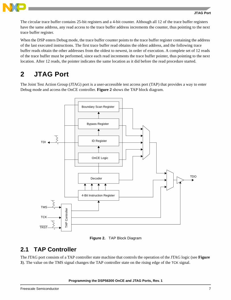
2 JTAG PortThe Joint Test Action Group (JTAG) port is a user-accessible test access port (TAP) that provides a way to enter Debug mode and access the OnCE controller. Figure 2 shows the TAP block diagram.
Figure 2. TAP Block Diagram
2.1 TAP ControllerThe JTAG port consists of a TAP controller state machine that controls the operation of the JTAG logic (see Figure 3). The value on the TMS signal changes the TAP controller state on the rising edge of the TCK signal.
TA
P C
ontr
olle
r
Decoder
4-Bit Instruction Register
OnCE Logic
ID Register
Boundary Scan Register
Bypass Register
TMS
TCK
TRST
TDI
TDO
Programming the DSP56300 OnCE and JTAG Ports, Rev. 1
Freescale Semiconductor 7
JTAG Port
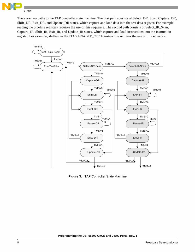
There are two paths to the TAP controller state machine. The first path consists of Select_DR_Scan, Capture_DR, Shift_DR, Exit_DR, and Update_DR states, which capture and load data into the test data register. For example, reading the pipeline registers requires the use of this sequence. The second path consists of Select_IR_Scan, Capture_IR, Shift_IR, Exit_IR, and Update_IR states, which capture and load instructions into the instruction register. For example, shifting in the JTAG ENABLE_ONCE instruction requires the use of this sequence.
Figure 3. TAP Controller State Machine
Test-Logic-Reset
Run-Test/Idle Select-DR-Scan
Capture-DR
Shift-DR
Exit1-DR
Pause-DR
Exit2-DR
Update-DR
Select-IR-Scan
Capture-IR
Shift-IR
Exit1-IR
Pause-IR
Exit2-IR
Update-IR
TMS=1
TMS=0
TMS=0
TMS=0
TMS=0
TMS=0
TMS=0TMS=0 TMS=0
TMS=0TMS=0
TMS=0 TMS=0
TMS=0 TMS=0
TMS=1 TMS=1 TMS=1
TMS=1 TMS=1
TMS=1
TMS=1
TMS=1
TMS=1
TMS=0 TMS=0
TMS=1 TMS=1
Programming the DSP56300 OnCE and JTAG Ports, Rev. 1
8 Freescale Semiconductor
JTAG Port
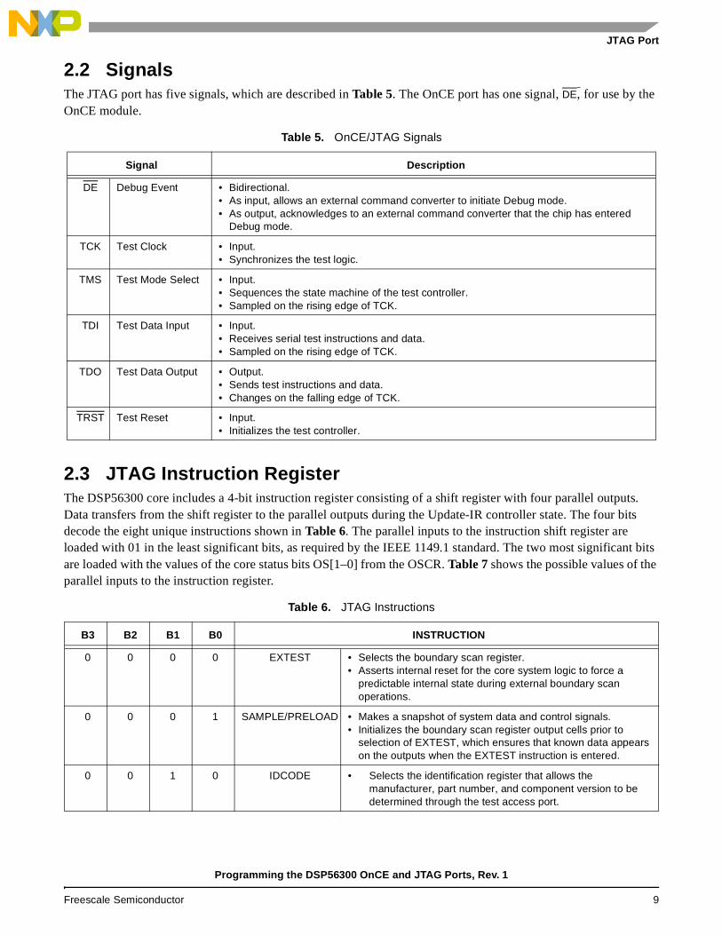
2.2 SignalsThe JTAG port has five signals, which are described in Table 5. The OnCE port has one signal, DE, for use by the OnCE module.
2.3 JTAG Instruction RegisterThe DSP56300 core includes a 4-bit instruction register consisting of a shift register with four parallel outputs. Data transfers from the shift register to the parallel outputs during the Update-IR controller state. The four bits decode the eight unique instructions shown in Table 6. The parallel inputs to the instruction shift register are loaded with 01 in the least significant bits, as required by the IEEE 1149.1 standard. The two most significant bits are loaded with the values of the core status bits OS[1–0] from the OSCR. Table 7 shows the possible values of the parallel inputs to the instruction register.
Table 5. OnCE/JTAG Signals
Signal Description
DE Debug Event • Bidirectional.• As input, allows an external command converter to initiate Debug mode.• As output, acknowledges to an external command converter that the chip has entered
Debug mode.
TCK Test Clock • Input.• Synchronizes the test logic.
TMS Test Mode Select • Input.• Sequences the state machine of the test controller.• Sampled on the rising edge of TCK.
TDI Test Data Input • Input.• Receives serial test instructions and data.• Sampled on the rising edge of TCK.
TDO Test Data Output • Output.• Sends test instructions and data.• Changes on the falling edge of TCK.
TRST Test Reset • Input.• Initializes the test controller.
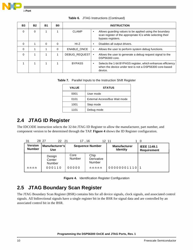
Table 6. JTAG Instructions
B3 B2 B1 B0 INSTRUCTION
0 0 0 0 EXTEST • Selects the boundary scan register.• Asserts internal reset for the core system logic to force a
predictable internal state during external boundary scan operations.
0 0 0 1 SAMPLE/PRELOAD • Makes a snapshot of system data and control signals.• Initializes the boundary scan register output cells prior to
selection of EXTEST, which ensures that known data appears on the outputs when the EXTEST instruction is entered.
0 0 1 0 IDCODE • Selects the identification register that allows the manufacturer, part number, and component version to be determined through the test access port.
Programming the DSP56300 OnCE and JTAG Ports, Rev. 1
Freescale Semiconductor 9
JTAG Port
2.4 JTAG ID RegisterThe IDCODE instruction selects the 32-bit JTAG ID Register to allow the manufacturer, part number, and component version to be determined through the TAP. Figure 4 shows the ID Register configuration.
Figure 4. Identification Register Configuration
2.5 JTAG Boundary Scan RegisterThe JTAG Boundary Scan Register (BSR) contains bits for all device signals, clock signals, and associated control signals. All bidirectional signals have a single register bit in the BSR for signal data and are controlled by an associated control bit in the BSR.
0 0 1 1 CLAMP • Allows guarding values to be applied using the boundary scan register of the appropriate ICs while selecting their bypass registers.
0 1 0 0 HI-Z • Disables all output drivers.
0 1 1 0 ENABLE_ONCE • Allows the user to perform system debug functions.
0 1 1 1 DEBUG_REQUEST • Allows the user to generate a debug request signal to the DSP56300 core.
1 1 1 1 BYPASS • Selects the 1-bit BYPASS register, which enhances efficiency when the device under test is not a DSP56300 core-based device.
Table 7. Parallel Inputs to the Instruction Shift Register
VALUE STATUS
0001 User mode
0101 External Access/Bus Wait mode
1001 Step mode
1101 Debug mode
Table 6. JTAG Instructions (Continued)
B3 B2 B1 B0 INSTRUCTION
01111231
n n n n 10 0 0 0 0 0 0 1 1 1 0
2122 1617
0 0 0 0 0 0 0 0 1 1 0 n n n n n
IEEE 1149.1Requirement
ManufacturerIdentity
DesignCenterNumber
2728
Manufacturer’sUse
CoreNumber
ChipDerivativeNumber
VersionNumber
Sequence Number
Programming the DSP56300 OnCE and JTAG Ports, Rev. 1
10 Freescale Semiconductor
Serial Protocol
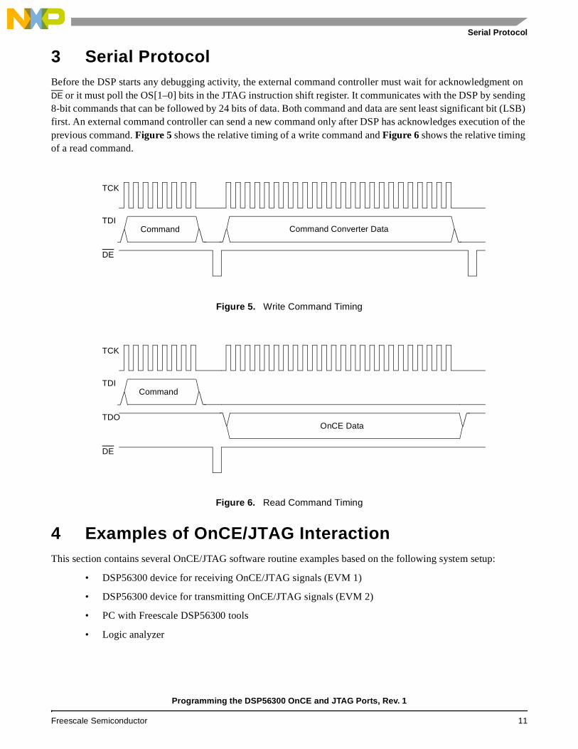
3 Serial ProtocolBefore the DSP starts any debugging activity, the external command controller must wait for acknowledgment on DE or it must poll the OS[1–0] bits in the JTAG instruction shift register. It communicates with the DSP by sending 8-bit commands that can be followed by 24 bits of data. Both command and data are sent least significant bit (LSB) first. An external command controller can send a new command only after DSP has acknowledges execution of the previous command. Figure 5 shows the relative timing of a write command and Figure 6 shows the relative timing of a read command.
Figure 5. Write Command Timing
Figure 6. Read Command Timing
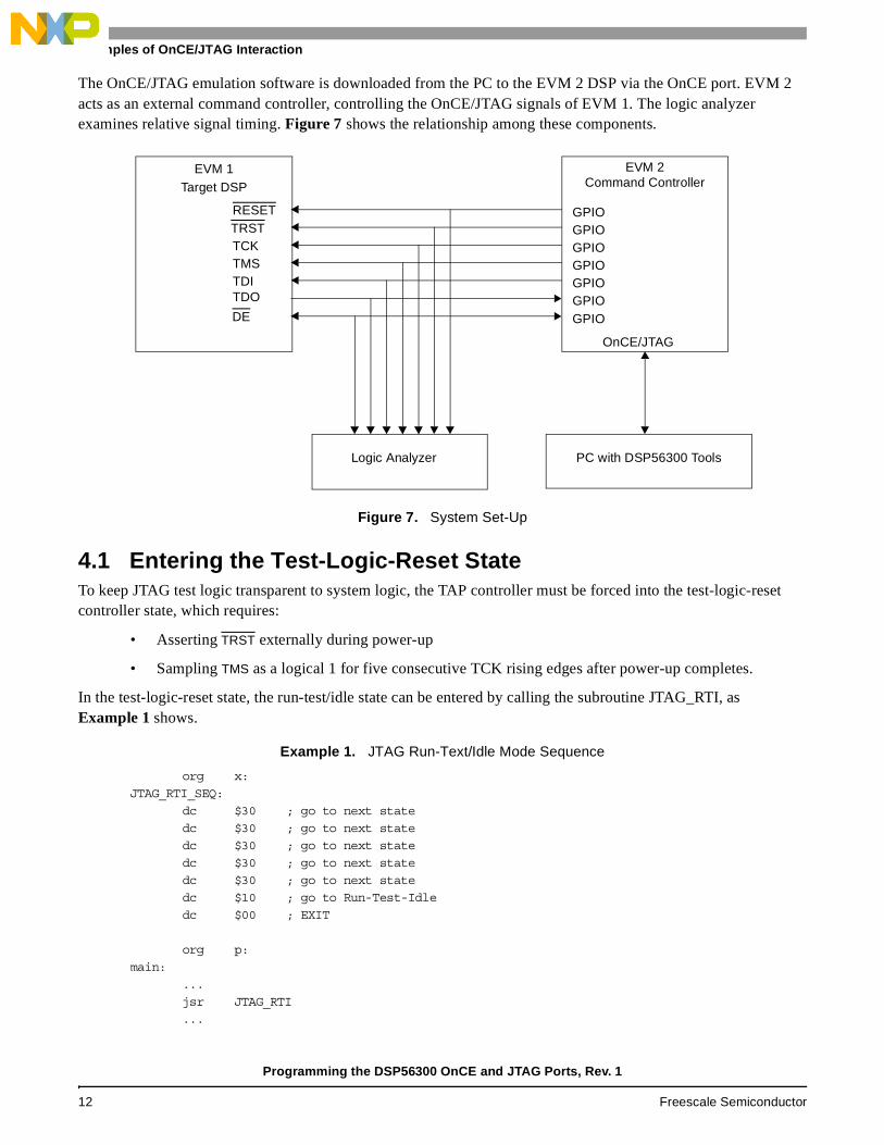
4 Examples of OnCE/JTAG InteractionThis section contains several OnCE/JTAG software routine examples based on the following system setup:
• DSP56300 device for receiving OnCE/JTAG signals (EVM 1)
• DSP56300 device for transmitting OnCE/JTAG signals (EVM 2)
• PC with Freescale DSP56300 tools
• Logic analyzer
TCK
TDI
DE
Command Command Converter Data
TCK
TDI
TDO
Command
OnCE Data
DE
Programming the DSP56300 OnCE and JTAG Ports, Rev. 1
Freescale Semiconductor 11
Examples of OnCE/JTAG Interaction
The OnCE/JTAG emulation software is downloaded from the PC to the EVM 2 DSP via the OnCE port. EVM 2 acts as an external command controller, controlling the OnCE/JTAG signals of EVM 1. The logic analyzer examines relative signal timing. Figure 7 shows the relationship among these components.
Figure 7. System Set-Up
4.1 Entering the Test-Logic-Reset StateTo keep JTAG test logic transparent to system logic, the TAP controller must be forced into the test-logic-reset controller state, which requires:
• Asserting TRST externally during power-up
• Sampling TMS as a logical 1 for five consecutive TCK rising edges after power-up completes.
In the test-logic-reset state, the run-test/idle state can be entered by calling the subroutine JTAG_RTI, as Example 1 shows.
Example 1. JTAG Run-Text/Idle Mode Sequence
org x:
JTAG_RTI_SEQ:
dc $30 ; go to next state
dc $30 ; go to next state
dc $30 ; go to next state
dc $30 ; go to next state
dc $30 ; go to next state
dc $10 ; go to Run-Test-Idle
dc $00 ; EXIT
org p:
main:
...
jsr JTAG_RTI
...
RESETTRSTTCKTMSTDITDO
DE
GPIO
EVM 1 EVM 2
PC with DSP56300 Tools
OnCE/JTAG
Logic Analyzer
GPIOGPIOGPIOGPIOGPIOGPIO
Command ControllerTarget DSP
Programming the DSP56300 OnCE and JTAG Ports, Rev. 1
12 Freescale Semiconductor
Examples of OnCE/JTAG Interaction
JTAG_RTI:
move #JTAG_RTI_SEQ,r0
jsr JTAG_EXECUTE
rts
The JTAG_RTI subroutine sends a sequence of 8-bit data to the JTAG_EXECUTE subroutine. Table 8 lists the JTAG_RTI subroutine bit definitions.
For example, a value of $30 indicates that TMS = 1, TDI = 1 are sent on the rising edge of TCK and TDO is not read on the falling edge of TCK. Thus, JTAG_RTI sends a value $30 five times to enter the test-reset-logic state and then sends a value of $10 (TMS = 0, TDI =1, TDO is not read) to enter the run-test/idle state.
The JTAG_EXECUTE subroutine shown in Example 2 emulates OnCE/JTAG operation. The JTAG_EXECUTE routine is repeated until an exit value of $00 is encountered. For example, when the JTAG_RTI sends an 8-bit data, the JTAG_EXECUTE first determines if bit 2 is set to indicate that TDO needs to be read. Next, the JTAG_EXECUTE subroutine determines the value of bit 5 and sets or clears the TMS value accordingly. Next, the subroutine determines the value of bit 4 and sets or clears the TDI value accordingly. The TCK signal is then toggled to send the values on the JTAG signals.
Example 2. JTAG_EXECUTE Subroutine
JTAG_EXECUTE:
move x:(r0)+,a1
tst a
beq done
move a1,x:JTAG_CMD
brclr #DATA_RD,x:JTAG_CMD,no_read
read_TDO
brclr #TDO_BIT,x:M_PDRD,TDO_CLR
TDO_SET
move #>1,a
bra no_read
TDO_CLR
move #>0,a
no_read
brclr #DATA_TMS,x:JTAG_CMD,TMS_CLR
TMS_SET
bset #TMS_BIT,x:M_PDRD
bra >cont1
TMS_CLR
bclr #TMS_BIT,x:M_PDRD
cont1
brclr #DATA_TDI,x:JTAG_CMD,TDI_CLR
TDI_SET
bset #TDI_BIT,x:M_PDRD
bra >cont2
TDI_CLR
bclr #TDI_BIT,x:M_PDRD
cont2
bset #TCK_BIT,x:M_PDRD
Table 8. JTAG_RTI Subroutine Bit Definitions
7–6 5 4 3 2 1–0
Reserved TMS to send TDI to send Reserved Read TDO Reserved
Programming the DSP56300 OnCE and JTAG Ports, Rev. 1
Freescale Semiconductor 13
Examples of OnCE/JTAG Interaction
rep #3
nop
bclr #TCK_BIT,x:M_PDRD
bra >JTAG_EXECUTE
done
rts
4.2 Executing the JTAG DEBUG_REQUEST InstructionWhen the TAP controller is in the run-test/idle state, the JTAG DEBUG_REQUEST instruction can be executed to assert an internal debug request signal. As Table 6, JTAG Instructions, on page 9 shows, to send the DEBUG_REQUEST instruction, the JTAG Instruction Register requires a value of 0111. Note that the most significant bit of the JTAG Instruction Register is sent first. Example 3 shows the JTAG DEBUG_REQUEST sequence.
Example 3. JTAG DEBUG_REQUEST Sequence
org x:
JTAG_DR_SEQ:
dc $30 ; go to Select DR
dc $30 ; go to Select IR
dc $10 ; go to Capture IR
dc $10 ; go to Shift IR
dc $14 ; go to Shift IR - 1
dc $14 ; go to Shift IR - 1
dc $14 ; go to Shift IR - 1
dc $24 ; go to Exit IR - 0
dc $30 ; go to Update IR
dc $10 ; go to Run-Test-Idle
dc $00 ; EXIT
org p:
main:
...
jsr JTAG_DR
...
JTAG_DR:
move #JTAG_DR_SEQ,r0
jsr JTAG_EXECUTE
rts
4.3 Executing the JTAG ENABLE_ONCE InstructionTo determine whether the DSP has entered Debug mode, the status of the JTAG Instruction Shift Register can be polled by shifting in the JTAG ENABLE_ONCE instruction and reading the status information that is shifted out. The JTAG Instruction Register requires a value of 0110 (see Table 6 on page 9). At the same time that the ENABLE_ONCE instruction is shifted in, the parallel inputs to the instruction shift register should have a value of 1101 to indicate that the DSP has entered Debug mode. (see Table 7, Parallel Inputs to the Instruction Shift Register, on page 10). Example 4 shows the JTAG ENABLE_ONCE sequence.
Programming the DSP56300 OnCE and JTAG Ports, Rev. 1
14 Freescale Semiconductor
Examples of OnCE/JTAG Interaction
Example 4. JTAG ENABLE_ONCE Instruction
org x:
JTAG_ENBL_ONCE_SEQ:
dc $30 ; go to Select DR
dc $30 ; go to Select IR
dc $10 ; go to Capture IR
dc $10 ; go to Shift IR
dc $04 ; go to Shift IR - 0
dc $14 ; go to Shift IR - 1
dc $14 ; go to Shift IR - 1
dc $24 ; go to Exit IR - 0
dc $30 ; go to Update IR
dc $10 ; go to Run-Test-Idle
dc $00 ; EXIT
org p:
main:
...
jsr JTAG_ENBL_ONCE
...
JTAG_ENBL_ONCE:
move #JTAG_ENBL_ONCE_SEQ,r0
jsr JTAG_EXECUTE
rts
Another way to determine whether the DSP has entered Debug mode is to monitor the DE signal. Every time the DSP acknowledges the execution of an instruction in Debug mode, it generates a pulse.
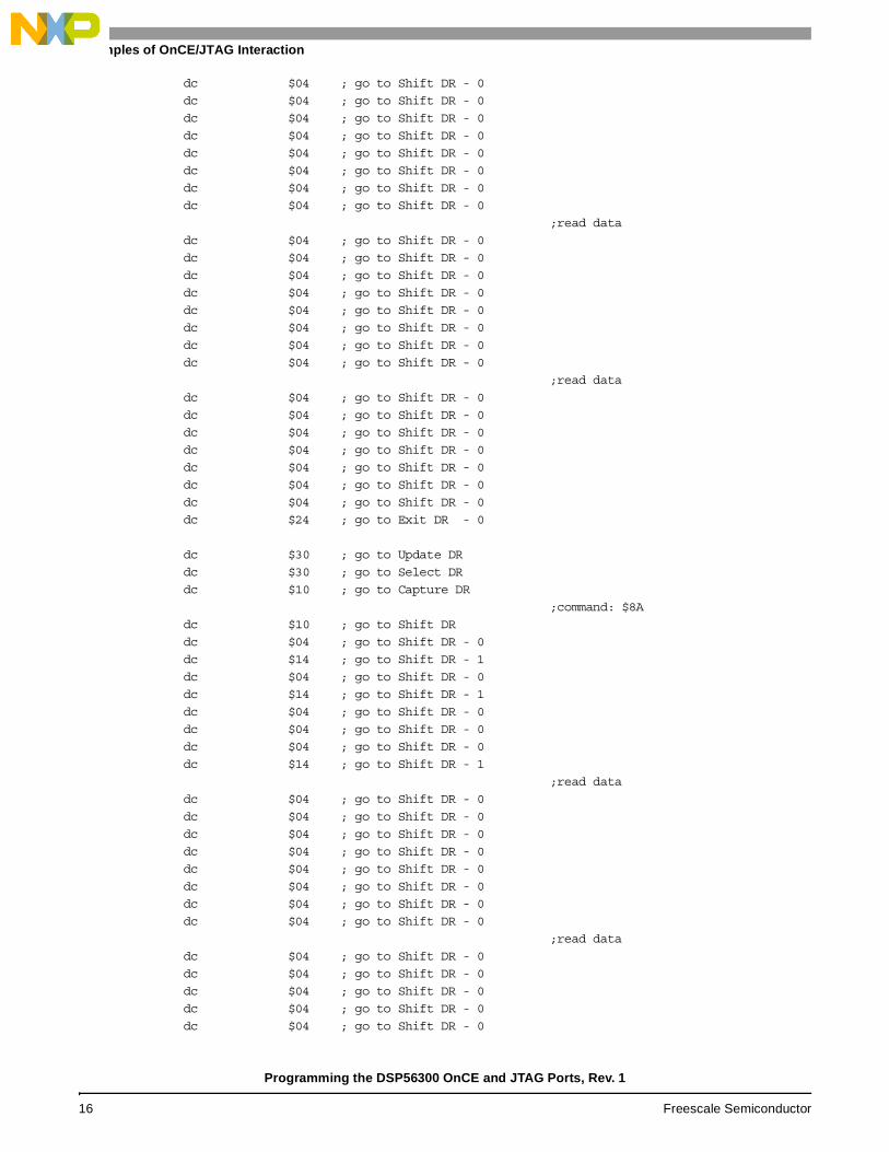
4.4 Reading the Pipeline RegistersAfter the JTAG instructions DEBUG_REQUEST and ENABLE_ONCE complete, and after the core status has been polled to verify that the DSP is in Debug mode, the pipeline must be saved before debugging starts. As Example 5 shows, reading the pipeline registers requires the following steps:
1. Send the 8-bit command $8B to read the OPILR, no GO, no EXIT and read the 24-bit data.
2. Send the 8-bit command $8A to read the OPDBR, no GO, no EXIT and read the 24-bit data.
Example 5. Pipeline Register Read Sequence
org x:
JTAG_PIPELN_RD_SEQ:
dc $30 ; go to Select DR
dc $10 ; go to Capture DR
;command: $8B
dc $10 ; go to Shift DR
dc $14 ; go to Shift DR - 1
dc $14 ; go to Shift DR - 1
dc $04 ; go to Shift DR - 0
dc $14 ; go to Shift DR - 1
dc $04 ; go to Shift DR - 0
dc $04 ; go to Shift DR - 0
dc $04 ; go to Shift DR - 0
dc $14 ; go to Shift DR - 1
;read data
Programming the DSP56300 OnCE and JTAG Ports, Rev. 1
Freescale Semiconductor 15
Examples of OnCE/JTAG Interaction
dc $04 ; go to Shift DR - 0
dc $04 ; go to Shift DR - 0
dc $04 ; go to Shift DR - 0
dc $04 ; go to Shift DR - 0
dc $04 ; go to Shift DR - 0
dc $04 ; go to Shift DR - 0
dc $04 ; go to Shift DR - 0
dc $04 ; go to Shift DR - 0
;read data
dc $04 ; go to Shift DR - 0
dc $04 ; go to Shift DR - 0
dc $04 ; go to Shift DR - 0
dc $04 ; go to Shift DR - 0
dc $04 ; go to Shift DR - 0
dc $04 ; go to Shift DR - 0
dc $04 ; go to Shift DR - 0
dc $04 ; go to Shift DR - 0
;read data
dc $04 ; go to Shift DR - 0
dc $04 ; go to Shift DR - 0
dc $04 ; go to Shift DR - 0
dc $04 ; go to Shift DR - 0
dc $04 ; go to Shift DR - 0
dc $04 ; go to Shift DR - 0
dc $04 ; go to Shift DR - 0
dc $24 ; go to Exit DR - 0
dc $30 ; go to Update DR
dc $30 ; go to Select DR
dc $10 ; go to Capture DR
;command: $8A
dc $10 ; go to Shift DR
dc $04 ; go to Shift DR - 0
dc $14 ; go to Shift DR - 1
dc $04 ; go to Shift DR - 0
dc $14 ; go to Shift DR - 1
dc $04 ; go to Shift DR - 0
dc $04 ; go to Shift DR - 0
dc $04 ; go to Shift DR - 0
dc $14 ; go to Shift DR - 1
;read data
dc $04 ; go to Shift DR - 0
dc $04 ; go to Shift DR - 0
dc $04 ; go to Shift DR - 0
dc $04 ; go to Shift DR - 0
dc $04 ; go to Shift DR - 0
dc $04 ; go to Shift DR - 0
dc $04 ; go to Shift DR - 0
dc $04 ; go to Shift DR - 0
;read data
dc $04 ; go to Shift DR - 0
dc $04 ; go to Shift DR - 0
dc $04 ; go to Shift DR - 0
dc $04 ; go to Shift DR - 0
dc $04 ; go to Shift DR - 0
Programming the DSP56300 OnCE and JTAG Ports, Rev. 1
16 Freescale Semiconductor
Examples of OnCE/JTAG Interaction
dc $04 ; go to Shift DR - 0
dc $04 ; go to Shift DR - 0
dc $04 ; go to Shift DR - 0
;read data
dc $04 ; go to Shift DR - 0
dc $04 ; go to Shift DR - 0
dc $04 ; go to Shift DR - 0
dc $04 ; go to Shift DR - 0
dc $04 ; go to Shift DR - 0
dc $04 ; go to Shift DR - 0
dc $04 ; go to Shift DR - 0
dc $24 ; go to Exit DR - 0
dc $30 ; go to Update DR
dc $10 ; go to Run-Test-Idle
dc $00 ; Exit
org p:
main:
...
jsr JTAG_PIPELN_RD
...
JTAG_XRAM_WR:
move #JTAG_PIPELN_RD_SEQ,r0
jsr JTAG_EXECUTE
rts
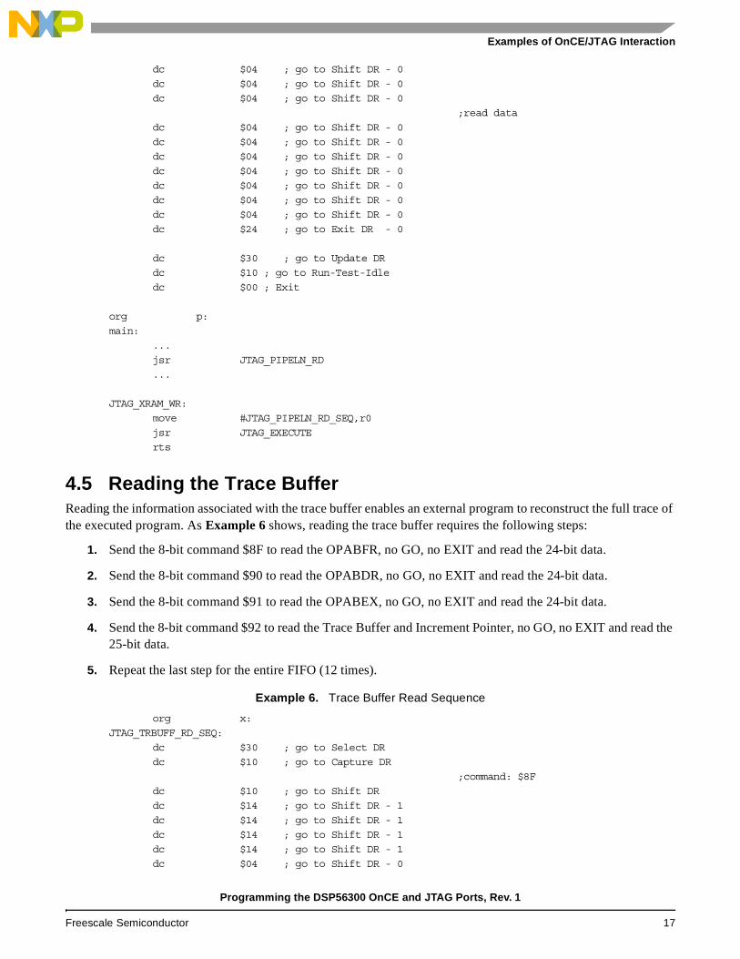
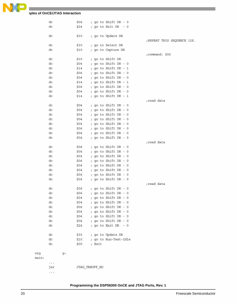
4.5 Reading the Trace BufferReading the information associated with the trace buffer enables an external program to reconstruct the full trace of the executed program. As Example 6 shows, reading the trace buffer requires the following steps:
1. Send the 8-bit command $8F to read the OPABFR, no GO, no EXIT and read the 24-bit data.
2. Send the 8-bit command $90 to read the OPABDR, no GO, no EXIT and read the 24-bit data.
3. Send the 8-bit command $91 to read the OPABEX, no GO, no EXIT and read the 24-bit data.
4. Send the 8-bit command $92 to read the Trace Buffer and Increment Pointer, no GO, no EXIT and read the 25-bit data.
5. Repeat the last step for the entire FIFO (12 times).
Example 6. Trace Buffer Read Sequence
org x:
JTAG_TRBUFF_RD_SEQ:
dc $30 ; go to Select DR
dc $10 ; go to Capture DR
;command: $8F
dc $10 ; go to Shift DR
dc $14 ; go to Shift DR - 1
dc $14 ; go to Shift DR - 1
dc $14 ; go to Shift DR - 1
dc $14 ; go to Shift DR - 1
dc $04 ; go to Shift DR - 0
Programming the DSP56300 OnCE and JTAG Ports, Rev. 1
Freescale Semiconductor 17
Examples of OnCE/JTAG Interaction
dc $04 ; go to Shift DR - 0
dc $04 ; go to Shift DR - 0
dc $14 ; go to Shift DR - 1
;read data
dc $04 ; go to Shift DR - 0
dc $04 ; go to Shift DR - 0
dc $04 ; go to Shift DR - 0
dc $04 ; go to Shift DR - 0
dc $04 ; go to Shift DR - 0
dc $04 ; go to Shift DR - 0
dc $04 ; go to Shift DR - 0
dc $04 ; go to Shift DR - 0
;read data
dc $04 ; go to Shift DR - 0
dc $04 ; go to Shift DR - 0
dc $04 ; go to Shift DR - 0
dc $04 ; go to Shift DR - 0
dc $04 ; go to Shift DR - 0
dc $04 ; go to Shift DR - 0
dc $04 ; go to Shift DR - 0
dc $04 ; go to Shift DR - 0
;read data
dc $04 ; go to Shift DR - 0
dc $04 ; go to Shift DR - 0
dc $04 ; go to Shift DR - 0
dc $04 ; go to Shift DR - 0
dc $04 ; go to Shift DR - 0
dc $04 ; go to Shift DR - 0
dc $04 ; go to Shift DR - 0
dc $24 ; go to Exit DR - 0
dc $30 ; go to Update DR
dc $30 ; go to Select DR
dc $10 ; go to Capture DR
;command: $90
dc $10 ; go to Shift DR
dc $04 ; go to Shift DR - 0
dc $04 ; go to Shift DR - 0
dc $04 ; go to Shift DR - 0
dc $04 ; go to Shift DR - 0
dc $14 ; go to Shift DR - 1
dc $04 ; go to Shift DR - 0
dc $04 ; go to Shift DR - 0
dc $14 ; go to Shift DR - 1
;read data
dc $04 ; go to Shift DR - 0
dc $04 ; go to Shift DR - 0
dc $04 ; go to Shift DR - 0
dc $04 ; go to Shift DR - 0
dc $04 ; go to Shift DR - 0
dc $04 ; go to Shift DR - 0
dc $04 ; go to Shift DR - 0
dc $04 ; go to Shift DR - 0
;read data
dc $04 ; go to Shift DR - 0
Programming the DSP56300 OnCE and JTAG Ports, Rev. 1
18 Freescale Semiconductor
Examples of OnCE/JTAG Interaction
dc $04 ; go to Shift DR - 0
dc $04 ; go to Shift DR - 0
dc $04 ; go to Shift DR - 0
dc $04 ; go to Shift DR - 0
dc $04 ; go to Shift DR - 0
dc $04 ; go to Shift DR - 0
dc $04 ; go to Shift DR - 0
;read data
dc $04 ; go to Shift DR - 0
dc $04 ; go to Shift DR - 0
dc $04 ; go to Shift DR - 0
dc $04 ; go to Shift DR - 0
dc $04 ; go to Shift DR - 0
dc $04 ; go to Shift DR - 0
dc $04 ; go to Shift DR - 0
dc $24 ; go to Exit DR - 0
dc $30 ; go to Update DR
dc $30 ; go to Select DR
dc $10 ; go to Capture DR
;command: $91
dc $10 ; go to Shift DR
dc $14 ; go to Shift DR - 1
dc $04 ; go to Shift DR - 0
dc $04 ; go to Shift DR - 0
dc $04 ; go to Shift DR - 0
dc $14 ; go to Shift DR - 1
dc $04 ; go to Shift DR - 0
dc $04 ; go to Shift DR - 0
dc $14 ; go to Shift DR - 1
;read data
dc $04 ; go to Shift DR - 0
dc $04 ; go to Shift DR - 0
dc $04 ; go to Shift DR - 0
dc $04 ; go to Shift DR - 0
dc $04 ; go to Shift DR - 0
dc $04 ; go to Shift DR - 0
dc $04 ; go to Shift DR - 0
dc $04 ; go to Shift DR - 0
;read data
dc $04 ; go to Shift DR - 0
dc $04 ; go to Shift DR - 0
dc $04 ; go to Shift DR - 0
dc $04 ; go to Shift DR - 0
dc $04 ; go to Shift DR - 0
dc $04 ; go to Shift DR - 0
dc $04 ; go to Shift DR - 0
dc $04 ; go to Shift DR - 0
;read data
dc $04 ; go to Shift DR - 0
dc $04 ; go to Shift DR - 0
dc $04 ; go to Shift DR - 0
dc $04 ; go to Shift DR - 0
dc $04 ; go to Shift DR - 0
dc $04 ; go to Shift DR - 0
Programming the DSP56300 OnCE and JTAG Ports, Rev. 1
Freescale Semiconductor 19
Examples of OnCE/JTAG Interaction
dc $04 ; go to Shift DR - 0
dc $24 ; go to Exit DR - 0
dc $30 ; go to Update DR
;REPEAT THIS SEQUENCE 12X.
dc $30 ; go to Select DR
dc $10 ; go to Capture DR
;command: $92
dc $10 ; go to Shift DR
dc $04 ; go to Shift DR - 0
dc $14 ; go to Shift DR - 1
dc $04 ; go to Shift DR - 0
dc $04 ; go to Shift DR - 0
dc $14 ; go to Shift DR - 1
dc $04 ; go to Shift DR - 0
dc $04 ; go to Shift DR - 0
dc $14 ; go to Shift DR - 1
;read data
dc $04 ; go to Shift DR - 0
dc $04 ; go to Shift DR - 0
dc $04 ; go to Shift DR - 0
dc $04 ; go to Shift DR - 0
dc $04 ; go to Shift DR - 0
dc $04 ; go to Shift DR - 0
dc $04 ; go to Shift DR - 0
dc $04 ; go to Shift DR - 0
;read data
dc $04 ; go to Shift DR - 0
dc $04 ; go to Shift DR - 0
dc $04 ; go to Shift DR - 0
dc $04 ; go to Shift DR - 0
dc $04 ; go to Shift DR - 0
dc $04 ; go to Shift DR - 0
dc $04 ; go to Shift DR - 0
dc $04 ; go to Shift DR - 0
;read data
dc $04 ; go to Shift DR - 0
dc $04 ; go to Shift DR - 0
dc $04 ; go to Shift DR - 0
dc $04 ; go to Shift DR - 0
dc $04 ; go to Shift DR - 0
dc $04 ; go to Shift DR - 0
dc $04 ; go to Shift DR - 0
dc $04 ; go to Shift DR - 0
dc $24 ; go to Exit DR - 0
dc $30 ; go to Update DR
dc $10 ; go to Run-Test-Idle
dc $00 ; Exit
org p:
main:
...
jsr JTAG_TRBUFF_RD
...
Programming the DSP56300 OnCE and JTAG Ports, Rev. 1
20 Freescale Semiconductor
Examples of OnCE/JTAG Interaction
JTAG_XRAM_WR:
move #JTAG_TRBUFF_RD_SEQ,r0
jsr JTAG_EXECUTE
rts
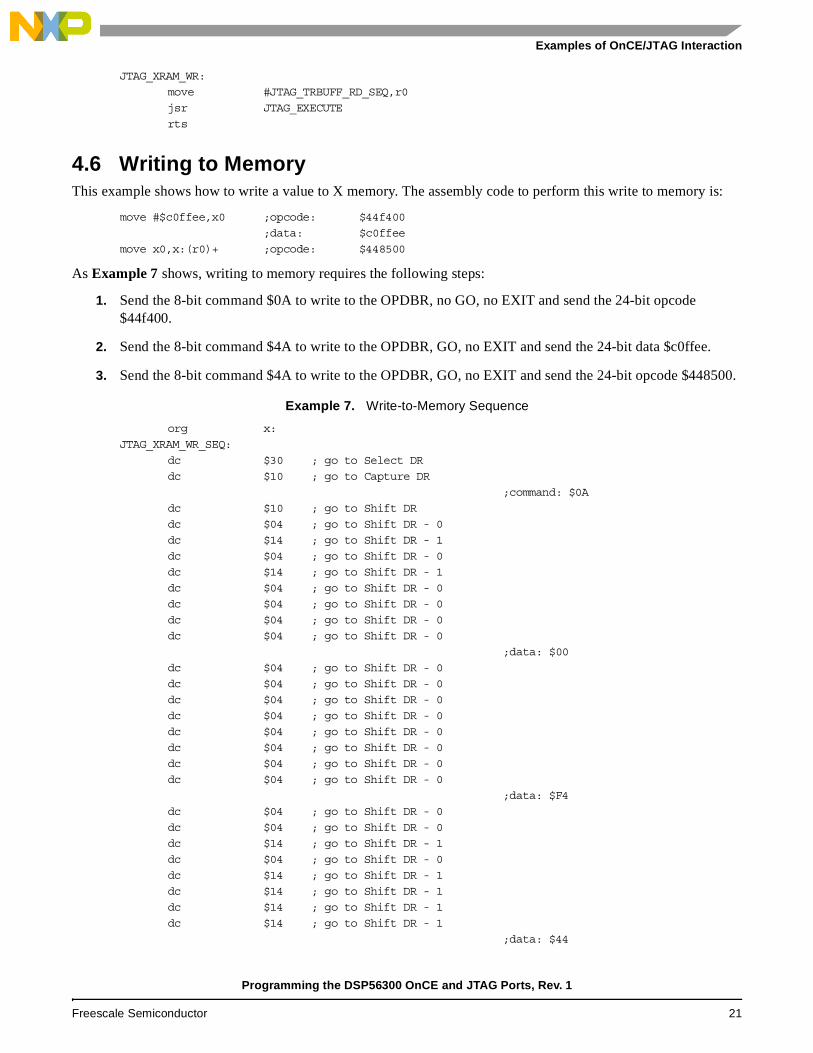
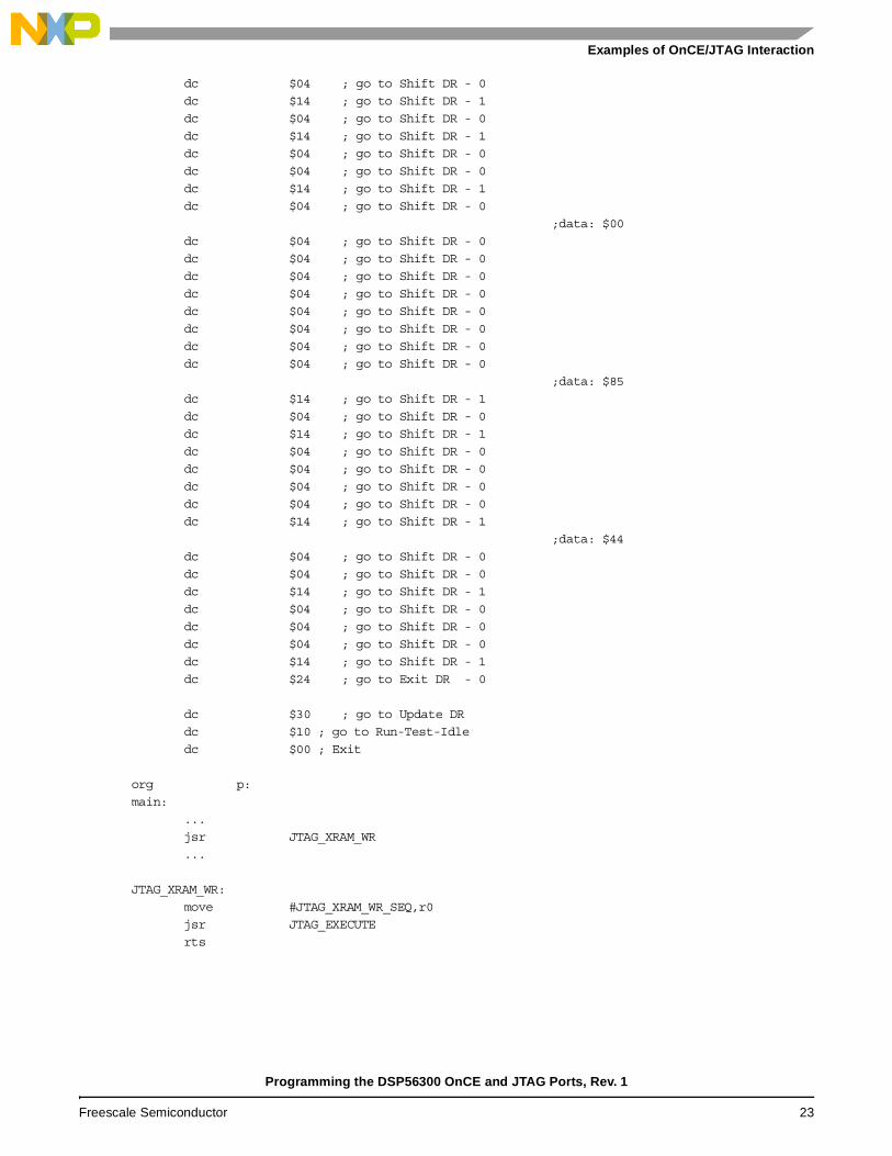
4.6 Writing to MemoryThis example shows how to write a value to X memory. The assembly code to perform this write to memory is:
move #$c0ffee,x0 ;opcode: $44f400
;data: $c0ffee
move x0,x:(r0)+ ;opcode: $448500
As Example 7 shows, writing to memory requires the following steps:
1. Send the 8-bit command $0A to write to the OPDBR, no GO, no EXIT and send the 24-bit opcode $44f400.
2. Send the 8-bit command $4A to write to the OPDBR, GO, no EXIT and send the 24-bit data $c0ffee.
3. Send the 8-bit command $4A to write to the OPDBR, GO, no EXIT and send the 24-bit opcode $448500.
Example 7. Write-to-Memory Sequence
org x:
JTAG_XRAM_WR_SEQ:
dc $30 ; go to Select DR
dc $10 ; go to Capture DR
;command: $0A
dc $10 ; go to Shift DR
dc $04 ; go to Shift DR - 0
dc $14 ; go to Shift DR - 1
dc $04 ; go to Shift DR - 0
dc $14 ; go to Shift DR - 1
dc $04 ; go to Shift DR - 0
dc $04 ; go to Shift DR - 0
dc $04 ; go to Shift DR - 0
dc $04 ; go to Shift DR - 0
;data: $00
dc $04 ; go to Shift DR - 0
dc $04 ; go to Shift DR - 0
dc $04 ; go to Shift DR - 0
dc $04 ; go to Shift DR - 0
dc $04 ; go to Shift DR - 0
dc $04 ; go to Shift DR - 0
dc $04 ; go to Shift DR - 0
dc $04 ; go to Shift DR - 0
;data: $F4
dc $04 ; go to Shift DR - 0
dc $04 ; go to Shift DR - 0
dc $14 ; go to Shift DR - 1
dc $04 ; go to Shift DR - 0
dc $14 ; go to Shift DR - 1
dc $14 ; go to Shift DR - 1
dc $14 ; go to Shift DR - 1
dc $14 ; go to Shift DR - 1
;data: $44
Programming the DSP56300 OnCE and JTAG Ports, Rev. 1
Freescale Semiconductor 21
Examples of OnCE/JTAG Interaction
dc $04 ; go to Shift DR - 0
dc $04 ; go to Shift DR - 0
dc $14 ; go to Shift DR - 1
dc $04 ; go to Shift DR - 0
dc $04 ; go to Shift DR - 0
dc $04 ; go to Shift DR - 0
dc $14 ; go to Shift DR - 1
dc $24 ; go to Exit DR - 0
dc $30 ; go to Update DR
dc $30 ; go to Select DR
dc $10 ; go to Capture DR
;command: $4A
dc $10 ; go to Shift DR
dc $04 ; go to Shift DR - 0
dc $14 ; go to Shift DR - 1
dc $04 ; go to Shift DR - 0
dc $14 ; go to Shift DR - 1
dc $04 ; go to Shift DR - 0
dc $04 ; go to Shift DR - 0
dc $14 ; go to Shift DR - 1
dc $04 ; go to Shift DR - 0
;data: $EE
dc $04 ; go to Shift DR - 0
dc $14 ; go to Shift DR - 1
dc $14 ; go to Shift DR - 1
dc $14 ; go to Shift DR - 1
dc $04 ; go to Shift DR - 0
dc $14 ; go to Shift DR - 1
dc $14 ; go to Shift DR - 1
dc $14 ; go to Shift DR - 1
;data: $FF
dc $14 ; go to Shift DR - 1
dc $14 ; go to Shift DR - 1
dc $14 ; go to Shift DR - 1
dc $14 ; go to Shift DR - 1
dc $14 ; go to Shift DR - 1
dc $14 ; go to Shift DR - 1
dc $14 ; go to Shift DR - 1
dc $14 ; go to Shift DR - 1
;data: $C0
dc $04 ; go to Shift DR - 0
dc $04 ; go to Shift DR - 0
dc $04 ; go to Shift DR - 0
dc $04 ; go to Shift DR - 0
dc $04 ; go to Shift DR - 0
dc $04 ; go to Shift DR - 0
dc $14 ; go to Shift DR - 1
dc $34 ; go to Exit DR - 1
;
dc $30 ; go to Update DR
dc $30 ; go to Select DR
dc $10 ; go to Capture DR
;command: $4A
dc $10 ; go to Shift DR
Programming the DSP56300 OnCE and JTAG Ports, Rev. 1
22 Freescale Semiconductor
Examples of OnCE/JTAG Interaction
dc $04 ; go to Shift DR - 0
dc $14 ; go to Shift DR - 1
dc $04 ; go to Shift DR - 0
dc $14 ; go to Shift DR - 1
dc $04 ; go to Shift DR - 0
dc $04 ; go to Shift DR - 0
dc $14 ; go to Shift DR - 1
dc $04 ; go to Shift DR - 0
;data: $00
dc $04 ; go to Shift DR - 0
dc $04 ; go to Shift DR - 0
dc $04 ; go to Shift DR - 0
dc $04 ; go to Shift DR - 0
dc $04 ; go to Shift DR - 0
dc $04 ; go to Shift DR - 0
dc $04 ; go to Shift DR - 0
dc $04 ; go to Shift DR - 0
;data: $85
dc $14 ; go to Shift DR - 1
dc $04 ; go to Shift DR - 0
dc $14 ; go to Shift DR - 1
dc $04 ; go to Shift DR - 0
dc $04 ; go to Shift DR - 0
dc $04 ; go to Shift DR - 0
dc $04 ; go to Shift DR - 0
dc $14 ; go to Shift DR - 1
;data: $44
dc $04 ; go to Shift DR - 0
dc $04 ; go to Shift DR - 0
dc $14 ; go to Shift DR - 1
dc $04 ; go to Shift DR - 0
dc $04 ; go to Shift DR - 0
dc $04 ; go to Shift DR - 0
dc $14 ; go to Shift DR - 1
dc $24 ; go to Exit DR - 0
dc $30 ; go to Update DR
dc $10 ; go to Run-Test-Idle
dc $00 ; Exit
org p:
main:
...
jsr JTAG_XRAM_WR
...
JTAG_XRAM_WR:
move #JTAG_XRAM_WR_SEQ,r0
jsr JTAG_EXECUTE
rts
Programming the DSP56300 OnCE and JTAG Ports, Rev. 1
Freescale Semiconductor 23
Examples of OnCE/JTAG Interaction
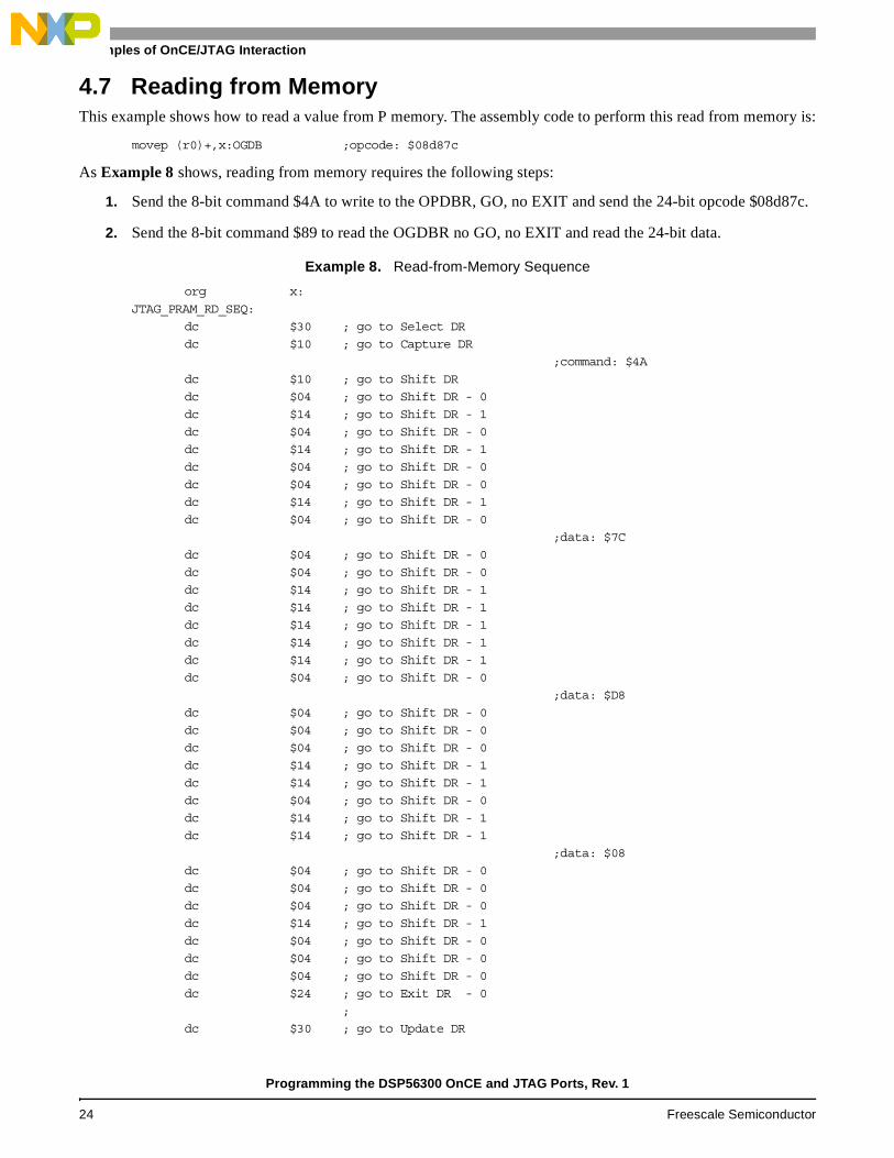
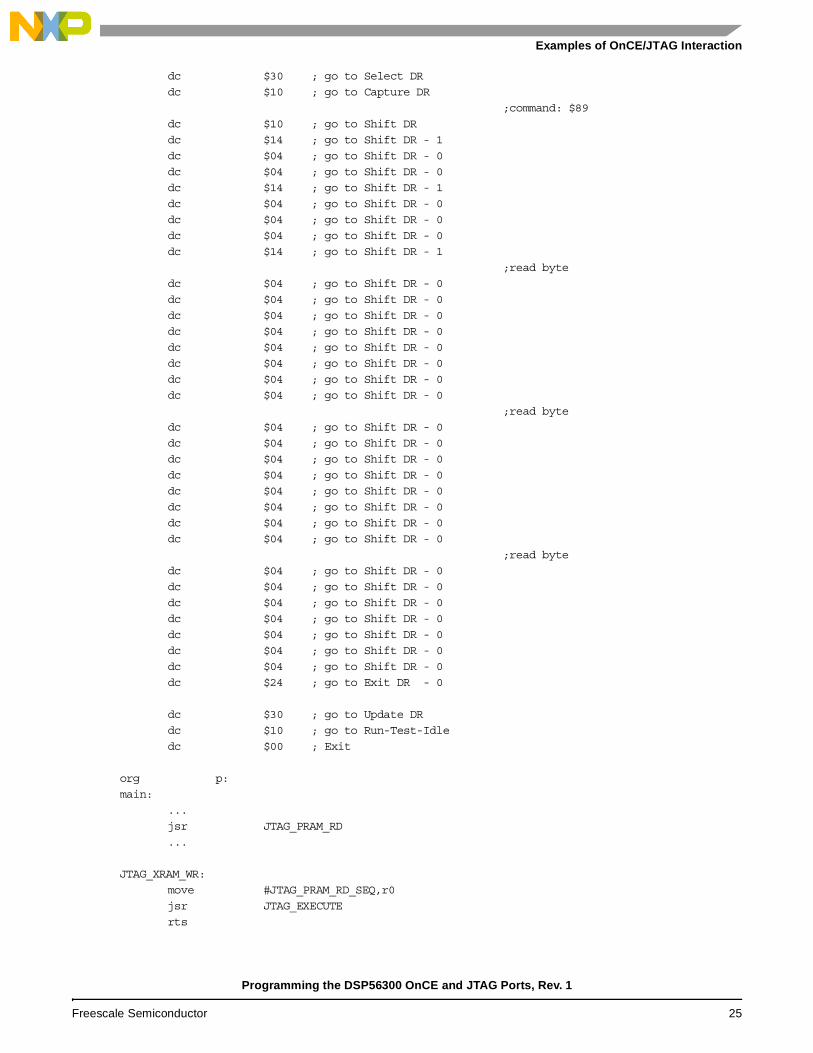
4.7 Reading from MemoryThis example shows how to read a value from P memory. The assembly code to perform this read from memory is:
movep (r0)+,x:OGDB ;opcode: $08d87c
As Example 8 shows, reading from memory requires the following steps:
1. Send the 8-bit command $4A to write to the OPDBR, GO, no EXIT and send the 24-bit opcode $08d87c.
2. Send the 8-bit command $89 to read the OGDBR no GO, no EXIT and read the 24-bit data.
Example 8. Read-from-Memory Sequence
org x:
JTAG_PRAM_RD_SEQ:
dc $30 ; go to Select DR
dc $10 ; go to Capture DR
;command: $4A
dc $10 ; go to Shift DR
dc $04 ; go to Shift DR - 0
dc $14 ; go to Shift DR - 1
dc $04 ; go to Shift DR - 0
dc $14 ; go to Shift DR - 1
dc $04 ; go to Shift DR - 0
dc $04 ; go to Shift DR - 0
dc $14 ; go to Shift DR - 1
dc $04 ; go to Shift DR - 0
;data: $7C
dc $04 ; go to Shift DR - 0
dc $04 ; go to Shift DR - 0
dc $14 ; go to Shift DR - 1
dc $14 ; go to Shift DR - 1
dc $14 ; go to Shift DR - 1
dc $14 ; go to Shift DR - 1
dc $14 ; go to Shift DR - 1
dc $04 ; go to Shift DR - 0
;data: $D8
dc $04 ; go to Shift DR - 0
dc $04 ; go to Shift DR - 0
dc $04 ; go to Shift DR - 0
dc $14 ; go to Shift DR - 1
dc $14 ; go to Shift DR - 1
dc $04 ; go to Shift DR - 0
dc $14 ; go to Shift DR - 1
dc $14 ; go to Shift DR - 1
;data: $08
dc $04 ; go to Shift DR - 0
dc $04 ; go to Shift DR - 0
dc $04 ; go to Shift DR - 0
dc $14 ; go to Shift DR - 1
dc $04 ; go to Shift DR - 0
dc $04 ; go to Shift DR - 0
dc $04 ; go to Shift DR - 0
dc $24 ; go to Exit DR - 0
;
dc $30 ; go to Update DR
Programming the DSP56300 OnCE and JTAG Ports, Rev. 1
24 Freescale Semiconductor
Examples of OnCE/JTAG Interaction
dc $30 ; go to Select DR
dc $10 ; go to Capture DR
;command: $89
dc $10 ; go to Shift DR
dc $14 ; go to Shift DR - 1
dc $04 ; go to Shift DR - 0
dc $04 ; go to Shift DR - 0
dc $14 ; go to Shift DR - 1
dc $04 ; go to Shift DR - 0
dc $04 ; go to Shift DR - 0
dc $04 ; go to Shift DR - 0
dc $14 ; go to Shift DR - 1
;read byte
dc $04 ; go to Shift DR - 0
dc $04 ; go to Shift DR - 0
dc $04 ; go to Shift DR - 0
dc $04 ; go to Shift DR - 0
dc $04 ; go to Shift DR - 0
dc $04 ; go to Shift DR - 0
dc $04 ; go to Shift DR - 0
dc $04 ; go to Shift DR - 0
;read byte
dc $04 ; go to Shift DR - 0
dc $04 ; go to Shift DR - 0
dc $04 ; go to Shift DR - 0
dc $04 ; go to Shift DR - 0
dc $04 ; go to Shift DR - 0
dc $04 ; go to Shift DR - 0
dc $04 ; go to Shift DR - 0
dc $04 ; go to Shift DR - 0
;read byte
dc $04 ; go to Shift DR - 0
dc $04 ; go to Shift DR - 0
dc $04 ; go to Shift DR - 0
dc $04 ; go to Shift DR - 0
dc $04 ; go to Shift DR - 0
dc $04 ; go to Shift DR - 0
dc $04 ; go to Shift DR - 0
dc $24 ; go to Exit DR - 0
dc $30 ; go to Update DR
dc $10 ; go to Run-Test-Idle
dc $00 ; Exit
org p:
main:
...
jsr JTAG_PRAM_RD
...
JTAG_XRAM_WR:
move #JTAG_PRAM_RD_SEQ,r0
jsr JTAG_EXECUTE
rts
Programming the DSP56300 OnCE and JTAG Ports, Rev. 1
Freescale Semiconductor 25
Examples of OnCE/JTAG Interaction
NOTES:
Programming the DSP56300 OnCE and JTAG Ports, Rev. 1
26 Freescale Semiconductor
Examples of OnCE/JTAG Interaction
NOTES:
Programming the DSP56300 OnCE and JTAG Ports, Rev. 1
Freescale Semiconductor 27
Document Order No.: AN1839
Information in this document is provided solely to enable system and software implementers to use Freescale Semiconductor products. There are no express or implied copyright licenses granted hereunder to design or fabricate any integrated circuits or integrated circuits based on the information in this document.
Freescale Semiconductor reserves the right to make changes without further notice to any products herein. Freescale Semiconductor makes no warranty, representation or guarantee regarding the suitability of its products for any particular purpose, nor does Freescale Semiconductor assume any liability arising out of the application or use of any product or circuit, and specifically disclaims any and all liability, including without limitation consequential or incidental damages. “Typical” parameters which may be provided in Freescale Semiconductor data sheets and/or specifications can and do vary in different applications and actual performance may vary over time. All operating parameters, including “Typicals” must be validated for each customer application by customer’s technical experts. Freescale Semiconductor does not convey any license under its patent rights nor the rights of others. Freescale Semiconductor products are not designed, intended, or authorized for use as components in systems intended for surgical implant into the body, or other applications intended to support or sustain life, or for any other application in which the failure of the Freescale Semiconductor product could create a situation where personal injury or death may occur. Should Buyer purchase or use Freescale Semiconductor products for any such unintended or unauthorized application, Buyer shall indemnify and hold Freescale Semiconductor and its officers, employees, subsidiaries, affiliates, and distributors harmless against all claims, costs, damages, and expenses, and reasonable attorney fees arising out of, directly or indirectly, any claim of personal injury or death associated with such unintended or unauthorized use, even if such claim alleges that Freescale Semiconductor was negligent regarding the design or manufacture of the part.
Freescale™ and the Freescale logo are trademarks of Freescale Semiconductor, Inc. All other product or service names are the property of their respective owners.
© Freescale Semiconductor, Inc. 2001, 2005.
How to Reach Us:Home Page:www.freescale.com
E-mail:[email protected]
USA/Europe or Locations not listed:Freescale Semiconductor Technical Information Center, CH3701300 N. Alma School RoadChandler, Arizona 85224+1-800-521-6274 or [email protected]
Europe, Middle East, and Africa:Freescale Halbleiter Deutschland GMBHTechnical Information CenterSchatzbogen 781829 München, Germany+44 1296 380 456 (English)+46 8 52200080 (English)+49 89 92103 559 (German)+33 1 69 35 48 48 (French)[email protected]
Japan:Freescale Semiconductor Japan Ltd. HeadquartersARCO Tower 15F1-8-1, Shimo-Meguro, Meguro-ku,Tokyo 153-0064, Japan0120 191014 or +81 3 5437 [email protected]
Asia/Pacific:Freescale Semiconductor Hong Kong Ltd.Technical Information Center2 Dai King StreetTai Po Industrial EstateTai Po, N.T. Hong Kong+800 2666 8080
For Literature Requests Only:Freescale Semiconductor Literature Distribution CenterP.O. Box 5405Denver, Colorado 802171-800-441-2447 or 303-675-2140Fax: [email protected]
Rev. 18/2005