Embed Size (px)
Citation preview
16.10.2014
Display Elektronik GmbH
DEM 128128A TMH-PW-N
1,44“ TFT
TFT MODULE
Product Specification Ver.: 4
DEM 128128A TMH-PW-N Production Specification
Version: 4 PAGE: 2
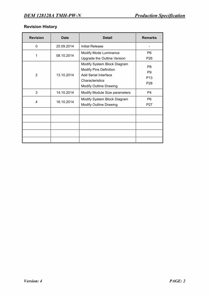
Revision History
Revision Date Detail Remarks
0 25.09.2014 Initial Release -
1 08.10.2014 Modify Mode Luminance Upgrade the Outline Version
P6 P26
2 13.10.2014
Modify System Block Diagram Modify Pins Definition Add Serial Interface Characteristics Modify Outline Drawing
P8 P9 P13 P28
3 14.10.2014 Modify Module Size parameters P4
4 16.10.2014 Modify System Block Diagram Modify Outline Drawing
P6 P27
DEM 128128A TMH-PW-N Production Specification
Version: 4 PAGE: 3
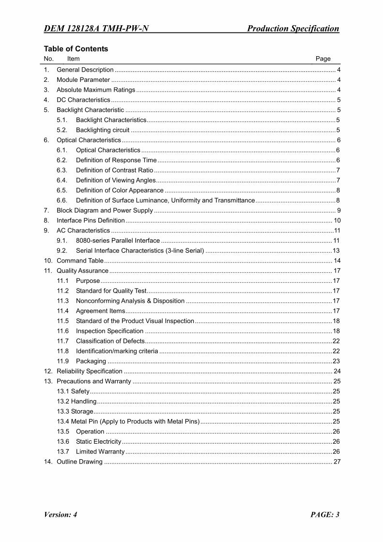
Table of Contents No. Item Page
1. General Description ............................................................................................................................ 4 2. Module Parameter .............................................................................................................................. 4 3. Absolute Maximum Ratings ................................................................................................................ 4 4. DC Characteristics .............................................................................................................................. 5 5. Backlight Characteristic ...................................................................................................................... 5
5.1. Backlight Characteristics .......................................................................................................... 5 5.2. Backlighting circuit ................................................................................................................... 5
6. Optical Characteristics ........................................................................................................................ 6 6.1. Optical Characteristics ............................................................................................................. 6 6.2. Definition of Response Time .................................................................................................... 6 6.3. Definition of Contrast Ratio ...................................................................................................... 7 6.4. Definition of Viewing Angles ..................................................................................................... 7 6.5. Definition of Color Appearance ................................................................................................ 8 6.6. Definition of Surface Luminance, Uniformity and Transmittance ............................................. 8
7. Block Diagram and Power Supply ...................................................................................................... 9 8. Interface Pins Definition .................................................................................................................... 10 9. AC Characteristics .............................................................................................................................11
9.1. 8080-series Parallel Interface ................................................................................................ 11 9.2. Serial Interface Characteristics (3-line Serial) ....................................................................... 13
10. Command Table ................................................................................................................................ 14 11. Quality Assurance ............................................................................................................................. 17
11.1 Purpose .................................................................................................................................. 17 11.2 Standard for Quality Test ........................................................................................................ 17 11.3 Nonconforming Analysis & Disposition .................................................................................. 17 11.4 Agreement Items .................................................................................................................... 17 11.5 Standard of the Product Visual Inspection ............................................................................. 18 11.6 Inspection Specification ......................................................................................................... 18 11.7 Classification of Defects ......................................................................................................... 22 11.8 Identification/marking criteria ................................................................................................. 22 11.9 Packaging .............................................................................................................................. 23
12. Reliability Specification ..................................................................................................................... 24 13. Precautions and Warranty ................................................................................................................ 25
13.1 Safety ........................................................................................................................................ 25 13.2 Handling .................................................................................................................................... 25 13.3 Storage ...................................................................................................................................... 25 13.4 Metal Pin (Apply to Products with Metal Pins) .......................................................................... 25 13.5 Operation ............................................................................................................................... 26 13.6 Static Electricity ...................................................................................................................... 26 13.7 Limited Warranty .................................................................................................................... 26
14. Outline Drawing ................................................................................................................................ 27
DEM 128128A TMH-PW-N Production Specification
Version: 4 PAGE: 4
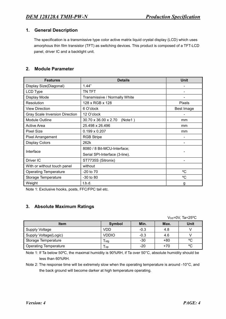
1. General Description
The specification is a transmissive type color active matrix liquid crystal display (LCD) which uses amorphous thin film transistor (TFT) as switching devices. This product is composed of a TFT-LCD panel, driver IC and a backlight unit.
2. Module Parameter
Features Details Unit Display Size(Diagonal) 1.44” - LCD Type TN TFT - Display Mode Transmissive / Normally White - Resolution 128 x RGB x 128 Pixels View Direction 6 O’clock Best Image Gray Scale Inversion Direction 12 O’clock - Module Outline 30.70 x 36.00 x 2.70 (Note1 ) mm Active Area 25.498 x 26.496 mm Pixel Size 0.199 x 0.207 mm Pixel Arrangement RGB Stripe - Display Colors 262k -
Interface 8080 / 8 Bit-MCU-Interface; Serial SPI-Interface (3-line).
-
Driver IC ST7735S (Sitronix) - With or without touch panel without Operating Temperature -20 to 70 ºC Storage Temperature -30 to 80 ºC Weight t.b.d. g Note 1: Exclusive hooks, posts, FFC/FPC tail etc.
3. Absolute Maximum Ratings
VSS=0V, Ta=25ºC Item Symbol Min. Max. Unit
Supply Voltage VDD -0.3 4.8 V Supply Voltage(Logic) VDDIO -0.3 4.6 V Storage Temperature Tstg -30 +80 ºC Operating Temperature Top -20 +70 ºC
Note 1: If Ta below 50ºC, the maximal humidity is 90%RH, if Ta over 50°C, absolute humidity should be less than 60%RH.
Note 2: The response time will be extremely slow when the operating temperature is around -10°C, and the back ground will become darker at high temperature operating.
DEM 128128A TMH-PW-N Production Specification
Version: 4 PAGE: 5
4. DC Characteristics
Item Symbol Min. Typ. Max. Unit
Supply Voltage VDD 2.6 2.75 3.3 V
VDDIO 1.65 1.9 3.3 V Logic Low Input Voltage VIL 0 - 0.3*VDDIO V Logic High Vnput Voltage VIH 0.7*VDDIO - VDDIO V Logic Low Output Voltage VOL GND - 0.2*VDDIO V Logic High Output Voltage VOH 0.8*VDDIO - VDDIO V Current Consumption Normal Mode ICC - 5 20 mA
5. Backlight Characteristic
5.1. Backlight Characteristics
Item Symbol Condition Min. Typ. Max. Unit Forward Voltage VF Ta=25 ºC, IF=20mA/LED 2.9 3.2 3.3 V Forward Current IF Ta=25 ºC, VF=3.2V/LED - 40 - mA Power Dissipation Pd - 64 - mW LED Lifetime - - 20000 hrs Uniformity Avg 80 85 - % Drive Method Constant current LED Configuration 2 White LED
Note: LED life time defined as follows: The final brightness is at 50% of original brightness. The environmental conducted under ambient air flow, at Ta=25±2 ºC, 60%RH±5%, IF=20mA.
5.2. Backlighting Circuit
A K
DEM 128128A TMH-PW-N Production Specification
Version: 4 PAGE: 6
6. Optical Characteristics
6.1. Optical Characteristics Ta=25ºC, DDV =2.75V, TN LC+ Polarizer
Bac
klig
ht O
n (T
rans
mis
sive
Mod
e)
Item Symbol Condition Specification
Unit Min. Typ. Max.
Luminance on
TFT( fI =20mA/LED) Lv
Normally viewing angle θX = φY =0º
240 300 - cd/m²
Contrast Ratio(See 6.3) CR - 350 - Response Time
(See 6.2) TR+TF - 25 40 ms
Chromaticity Transmissive
(See 6.5)
Red XR
(0.406) (0.556) (0.606) YR (0.264) (0.314) (0.364)
Green XG (0.247) (0.297) (0.347) YG (0.540) (0.590) (0.640)
Blue XB (0.091) (0.141) (0.191) YB (0.039) (0.089) (0.139)
White XW (0.195) (0.245) (0.295) YW (0.229) (0.279) (0.329)
Viewing Angle
(See 6.4)
Horizontal θX+
Center CR≥10
35 45 -
Deg. θX- 35 45 -
Vertical φY+ 35 45 - φY- 15 25 -
NTSC Ratio(Gamut) - 53 - %
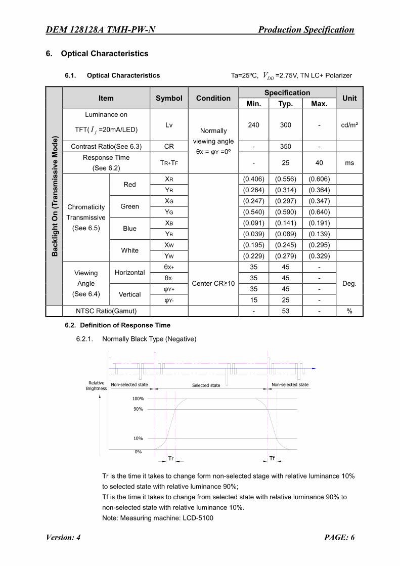
6.2. Definition of Response Time
6.2.1. Normally Black Type (Negative)
Selected stateNon-selected state
Tr Tf
Relative Brightness
100%
90%
10%
0%
Non-selected state
Tr is the time it takes to change form non-selected stage with relative luminance 10% to selected state with relative luminance 90%; Tf is the time it takes to change from selected state with relative luminance 90% to non-selected state with relative luminance 10%. Note: Measuring machine: LCD-5100
DEM 128128A TMH-PW-N Production Specification
Version: 4 PAGE: 7
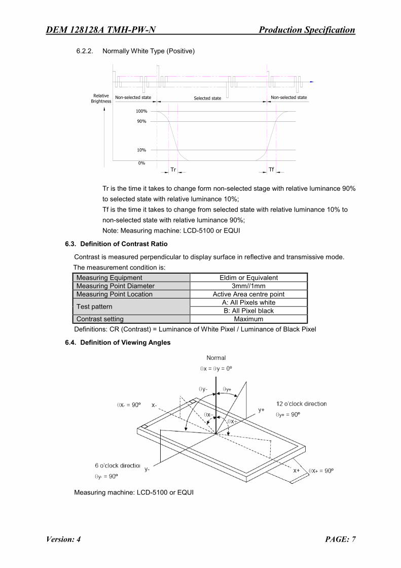
6.2.2. Normally White Type (Positive)
Selected stateNon-selected state
Tr Tf
Relative Brightness
100%
90%
10%
0%
Non-selected state
Tr is the time it takes to change form non-selected stage with relative luminance 90% to selected state with relative luminance 10%; Tf is the time it takes to change from selected state with relative luminance 10% to non-selected state with relative luminance 90%; Note: Measuring machine: LCD-5100 or EQUI
6.3. Definition of Contrast Ratio
Contrast is measured perpendicular to display surface in reflective and transmissive mode. The measurement condition is: Measuring Equipment Eldim or Equivalent Measuring Point Diameter 3mm//1mm Measuring Point Location Active Area centre point
Test pattern A: All Pixels white B: All Pixel black
Contrast setting Maximum Definitions: CR (Contrast) = Luminance of White Pixel / Luminance of Black Pixel
6.4. Definition of Viewing Angles
Measuring machine: LCD-5100 or EQUI
DEM 128128A TMH-PW-N Production Specification
Version: 4 PAGE: 8
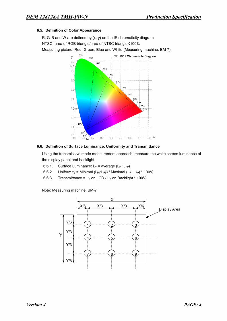
6.5. Definition of Color Appearance
R, G, B and W are defined by (x, y) on the IE chromaticity diagram NTSC=area of RGB triangle/area of NTSC triangleX100% Measuring picture: Red, Green, Blue and White (Measuring machine: BM-7)
6.6. Definition of Surface Luminance, Uniformity and Transmittance
Using the transmissive mode measurement approach, measure the white screen luminance of the display panel and backlight.
6.6.1. Surface Luminance: LV = average (LP1:LP9) 6.6.2. Uniformity = Minimal (LP1:LP9) / Maximal (LP1:LP9) * 100% 6.6.3. Transmittance = LV on LCD / LV on Backlight * 100%
Note: Measuring machine: BM-7
X
Y c
X/6 X/3 X/3 X/6
Y/6
Y/3
Y/3
Y/6
1 2 3
4 5 6
7 8 9
Display Area
DEM 128128A TMH-PW-N Production Specification
Version: 4 PAGE: 9
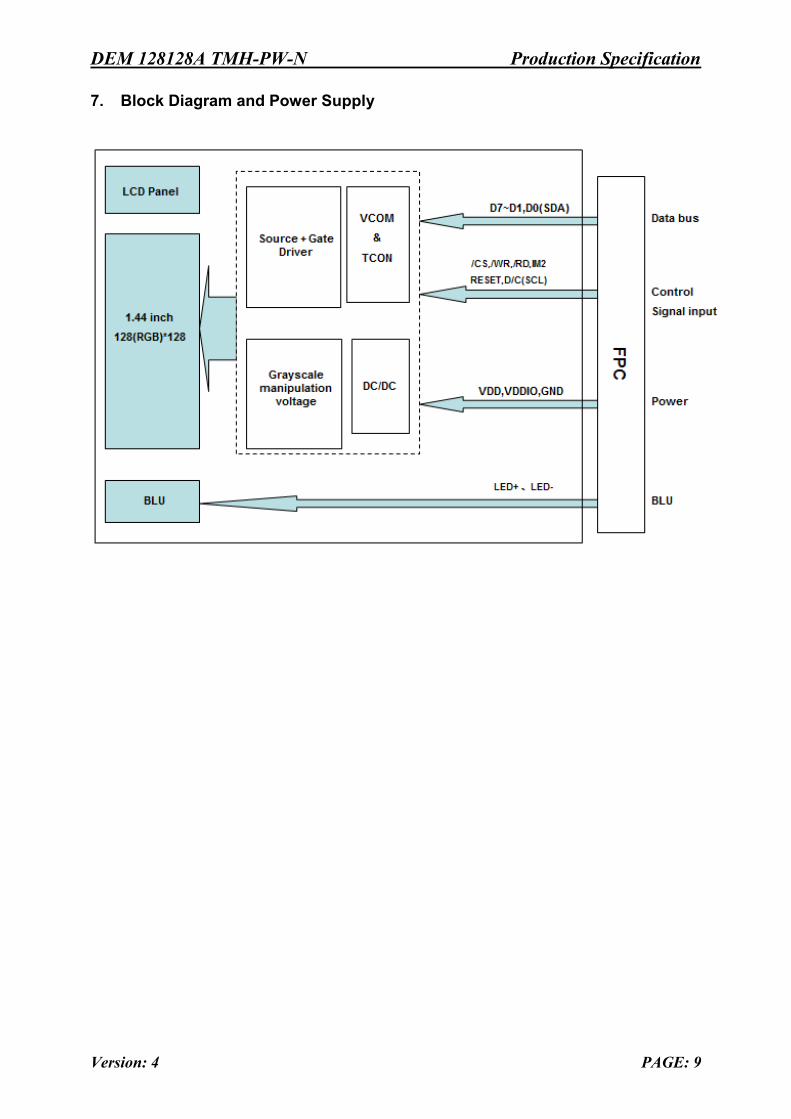
7. Block Diagram and Power Supply
DEM 128128A TMH-PW-N Production Specification
Version: 4 PAGE: 10
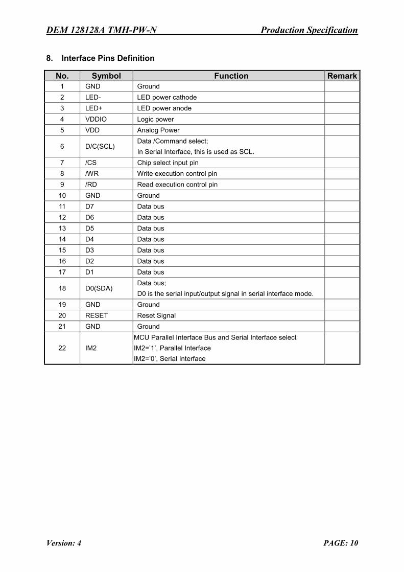
8. Interface Pins Definition
No. Symbol Function Remark 1 GND Ground 2 LED- LED power cathode 3 LED+ LED power anode 4 VDDIO Logic power 5 VDD Analog Power
6 D/C(SCL) Data /Command select; In Serial Interface, this is used as SCL.
7 /CS Chip select input pin 8 /WR Write execution control pin 9 /RD Read execution control pin 10 GND Ground 11 D7 Data bus 12 D6 Data bus 13 D5 Data bus 14 D4 Data bus 15 D3 Data bus 16 D2 Data bus 17 D1 Data bus
18 D0(SDA) Data bus; D0 is the serial input/output signal in serial interface mode.
19 GND Ground 20 RESET Reset Signal 21 GND Ground
22 IM2 MCU Parallel Interface Bus and Serial Interface select IM2=’1’, Parallel Interface IM2=’0’, Serial Interface
DEM 128128A TMH-PW-N Production Specification
Version: 4 PAGE: 11
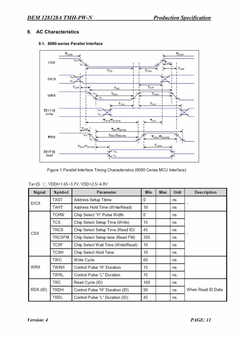
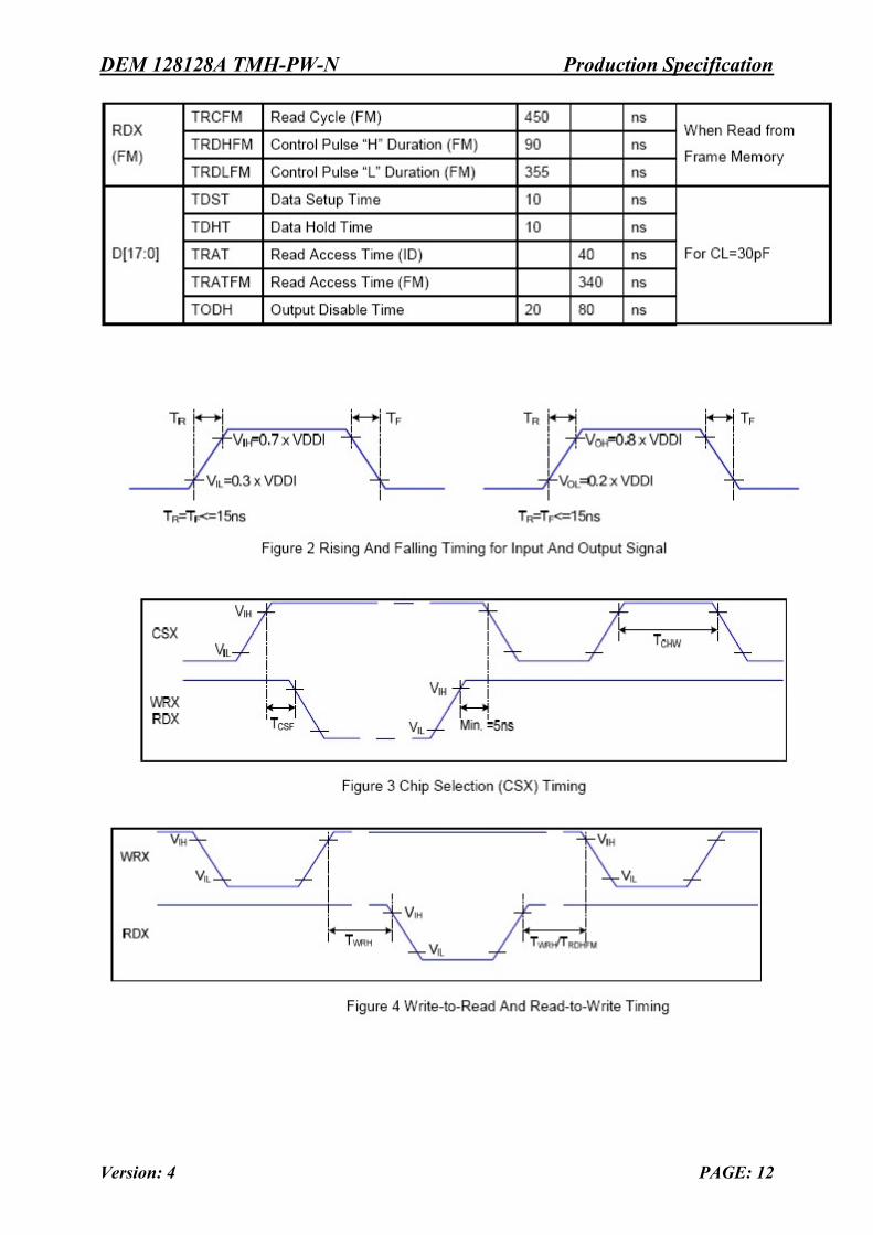
9. AC Characteristics
9.1. 8080-series Parallel Interface
DEM 128128A TMH-PW-N Production Specification
Version: 4 PAGE: 12
DEM 128128A TMH-PW-N Production Specification
Version: 4 PAGE: 13
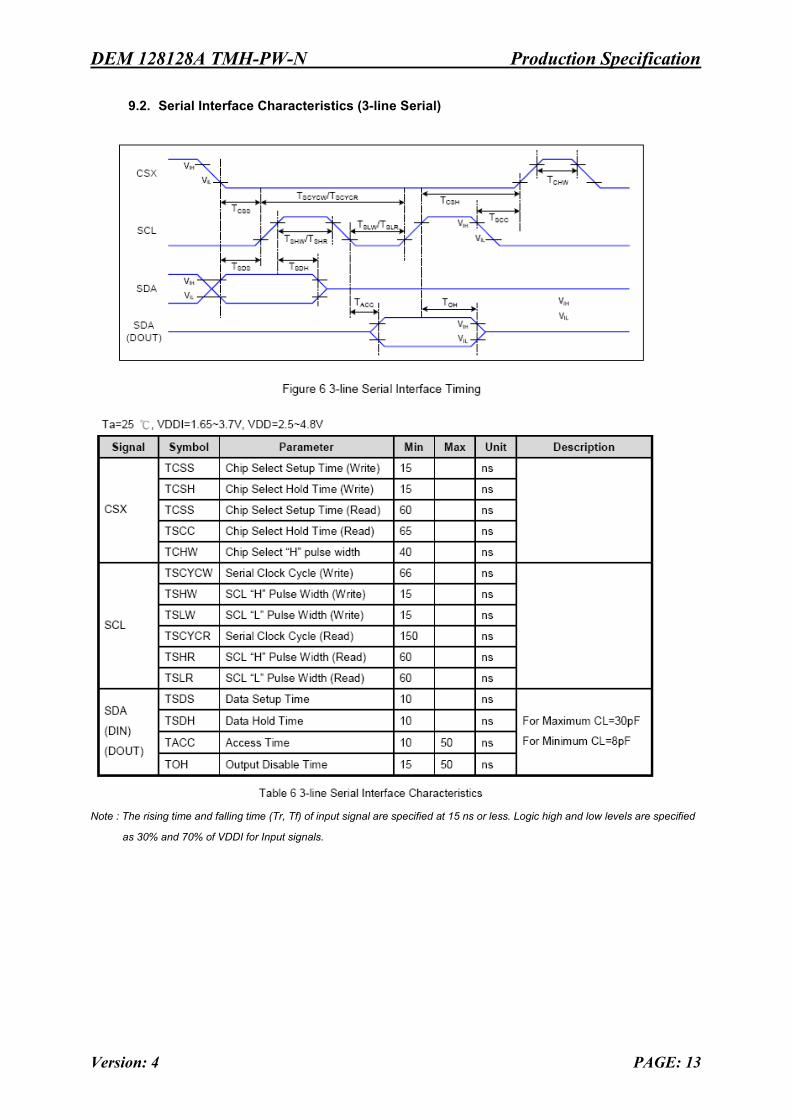
9.2. Serial Interface Characteristics (3-line Serial)
Note : The rising time and falling time (Tr, Tf) of input signal are specified at 15 ns or less. Logic high and low levels are specified
as 30% and 70% of VDDI for Input signals.
DEM 128128A TMH-PW-N Production Specification
Version: 4 PAGE: 14
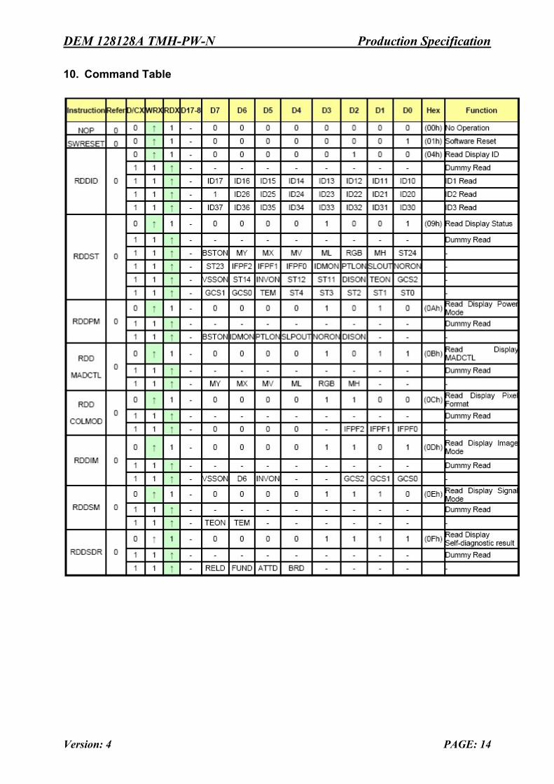
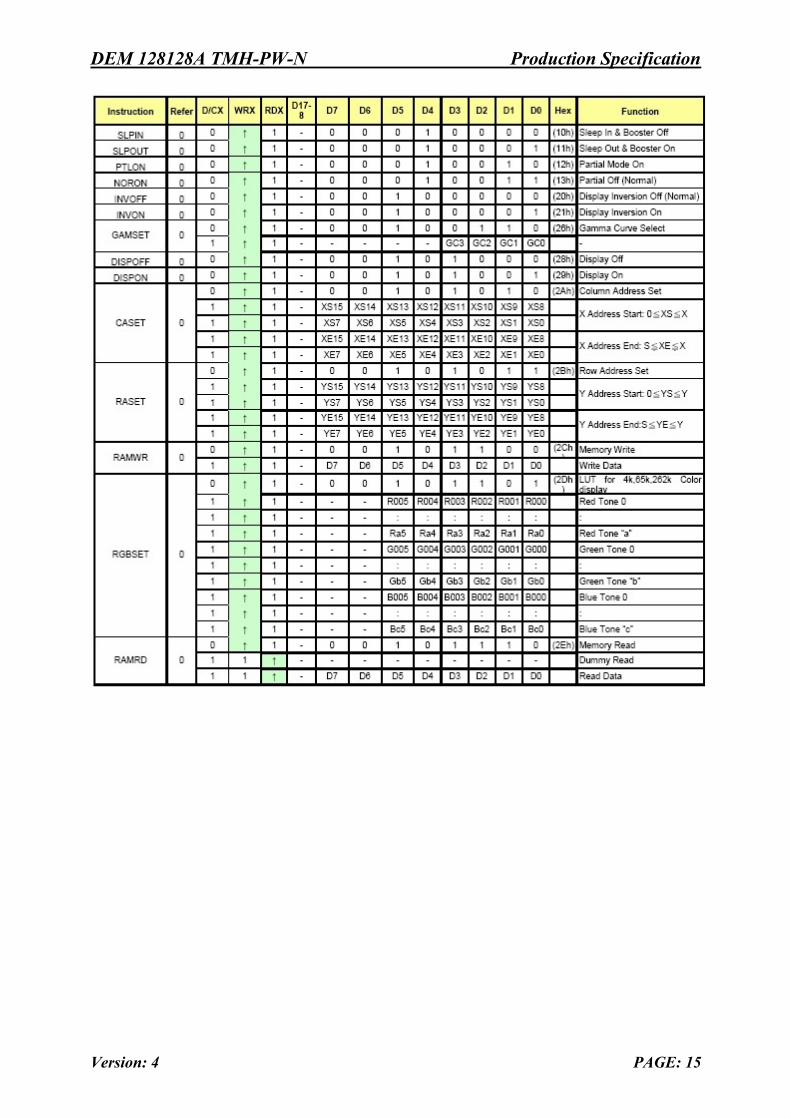
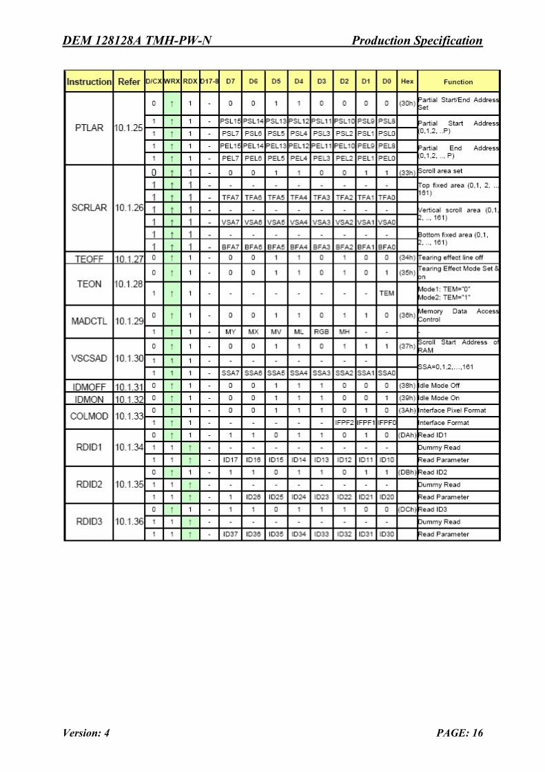
10. Command Table
DEM 128128A TMH-PW-N Production Specification
Version: 4 PAGE: 15
DEM 128128A TMH-PW-N Production Specification
Version: 4 PAGE: 16
DEM 128128A TMH-PW-N Production Specification
Version: 4 PAGE: 17
11. Quality Assurance
11.1 Purpose
This standard for Quality Assurance assures the quality of LCD module products supplied to customer.
11.2 Standard for Quality Test
11.2.1 Sampling Plan: GB2828.1-2003 Single sampling, general inspection level II 11.2.2 Sampling Criteria: Visual inspection: AQL 1.5% Electrical functional: AQL 0.65%. 11.2.3 Reliability Test: Detailed requirement refer to Reliability Test Specification.
11.3 Nonconforming Analysis & Disposition
11.3.1 Nonconforming analysis: 11.3.1.1 Customer should provide overall information of non-conforming sample for their
complaints. 11.3.1.2 After receipt of detailed information from customer, the analysis of nonconforming parts
usually should be finished in one week. 11.3.1.3 If can not finish the analysis on time, customer will be notified with the progress status. 11.3.2 Disposition of nonconforming: 11.3.2.1 Non-conforming product over PPM level will be replaced. 11.3.2.2 The cause of non-conformance will be analyzed. Corrective action will be discussed
and implemented.
11.4 Agreement Items
Shall negotiate with customer if the following situation occurs: 11.4.1 There is any discrepancy in standard of quality assurance. 11.4.2 Additional requirement to be added in product specification.
11.4.3 Any other special problem.
DEM 128128A TMH-PW-N Production Specification
Version: 4 PAGE: 18
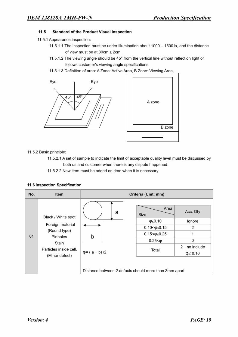
11.5 Standard of the Product Visual Inspection
11.5.1 Appearance inspection: 11.5.1.1 The inspection must be under illumination about 1000 – 1500 lx, and the distance
of view must be at 30cm ± 2cm. 11.5.1.2 The viewing angle should be 45° from the vertical line without reflection light or
follows customer's viewing angle specifications. 11.5.1.3 Definition of area: A Zone: Active Area, B Zone: Viewing Area,
11.5.2 Basic principle: 11.5.2.1 A set of sample to indicate the limit of acceptable quality level must be discussed by
both us and customer when there is any dispute happened. 11.5.2.2 New item must be added on time when it is necessary.
11.6 Inspection Specification
No. Item Criteria (Unit: mm)
01
Black / White spot
Foreign material (Round type)
Pinholes Stain
Particles inside cell. (Minor defect)
φ= ( a + b) /2 Distance between 2 defects should more than 3mm apart.
Area Size
Acc. Qty
φ≤0.10 Ignore 0.10<φ≤0.15 2 0.15<φ≤0.25 1
0.25<φ 0
Total 2 no include
φ≤ 0.10
A zone
B zone
45° 45°
Eye Eye
a
b
DEM 128128A TMH-PW-N Production Specification
Version: 4 PAGE: 19
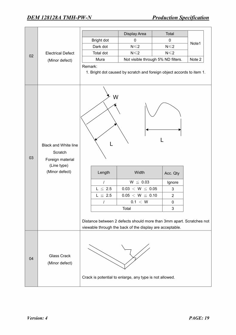
02 Electrical Defect
(Minor defect)
Display Area Total
Note1 Bright dot 0 0 Dark dot N≤2 N≤2 Total dot N≤2 N≤2
Mura Not visible through 5% ND filters. Note 2
Remark: 1. Bright dot caused by scratch and foreign object accords to item 1.
03
Black and White line
Scratch
Foreign material (Line type)
(Minor defect)
Length Width Acc. Qty
/ W ≦ 0.03 Ignore L ≦ 2.5 0.03 < W ≦ 0.05 3 L ≦ 2.5 0.05 < W ≦ 0.10 2
/ 0.1 < W 0 Total 3
Distance between 2 defects should more than 3mm apart. Scratches not viewable through the back of the display are acceptable.
04 Glass Crack
(Minor defect)
Crack is potential to enlarge, any type is not allowed.
W
L L
DEM 128128A TMH-PW-N Production Specification
Version: 4 PAGE: 20
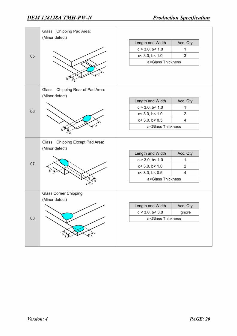
05
Glass Chipping Pad Area: (Minor defect)
Length and Width Acc. Qty c > 3.0, b< 1.0 1 c< 3.0, b< 1.0 3
a<Glass Thickness
06
Glass Chipping Rear of Pad Area: (Minor defect)
Length and Width Acc. Qty c > 3.0, b< 1.0 1 c< 3.0, b< 1.0 2 c< 3.0, b< 0.5 4
a<Glass Thickness
07
Glass Chipping Except Pad Area: (Minor defect)
Length and Width Acc. Qty c > 3.0, b< 1.0 1 c< 3.0, b< 1.0 2 c< 3.0, b< 0.5 4
a<Glass Thickness
08
Glass Corner Chipping: (Minor defect)
Length and Width Acc. Qty c < 3.0, b< 3.0 Ignore
a<Glass Thickness
DEM 128128A TMH-PW-N Production Specification
Version: 4 PAGE: 21
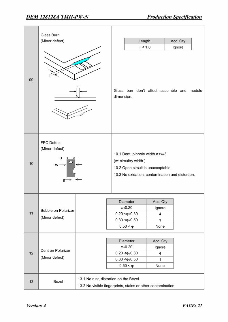
09
Glass Burr: (Minor defect)
Glass burr don’t affect assemble and module dimension.
Length Acc. Qty F < 1.0 Ignore
10
FPC Defect: (Minor defect)
10.1 Dent, pinhole width a<w/3.
(w: circuitry width.)
10.2 Open circuit is unacceptable.
10.3 No oxidation, contamination and distortion.
11 Bubble on Polarizer
(Minor defect)
Diameter Acc. Qty φ≤0.20 Ignore
0.20 <φ≤0.30 4 0.30 <φ≤0.50 1
0.50 < φ None
12 Dent on Polarizer
(Minor defect)
Diameter Acc. Qty φ≤0.20 Ignore
0.20 <φ≤0.30 4 0.30 <φ≤0.50 1
0.50 < φ None
13 Bezel 13.1 No rust, distortion on the Bezel.
13.2 No visible fingerprints, stains or other contamination.
a
w a
DEM 128128A TMH-PW-N Production Specification
Version: 4 PAGE: 22
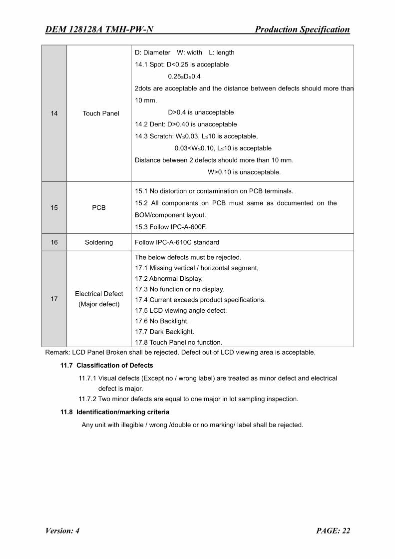
14 Touch Panel
D: Diameter W: width L: length 14.1 Spot: D<0.25 is acceptable
0.25≤D≤0.4
2dots are acceptable and the distance between defects should more than
10 mm.
D>0.4 is unacceptable
14.2 Dent: D>0.40 is unacceptable
14.3 Scratch: W≤0.03, L≤10 is acceptable,
0.03<W≤0.10, L≤10 is acceptable
Distance between 2 defects should more than 10 mm.
W>0.10 is unacceptable.
15 PCB
15.1 No distortion or contamination on PCB terminals.
15.2 All components on PCB must same as documented on the
BOM/component layout.
15.3 Follow IPC-A-600F.
16 Soldering Follow IPC-A-610C standard
17 Electrical Defect (Major defect)
The below defects must be rejected. 17.1 Missing vertical / horizontal segment, 17.2 Abnormal Display. 17.3 No function or no display. 17.4 Current exceeds product specifications. 17.5 LCD viewing angle defect. 17.6 No Backlight. 17.7 Dark Backlight. 17.8 Touch Panel no function.
Remark: LCD Panel Broken shall be rejected. Defect out of LCD viewing area is acceptable.
11.7 Classification of Defects
11.7.1 Visual defects (Except no / wrong label) are treated as minor defect and electrical defect is major.
11.7.2 Two minor defects are equal to one major in lot sampling inspection.
11.8 Identification/marking criteria
Any unit with illegible / wrong /double or no marking/ label shall be rejected.
DEM 128128A TMH-PW-N Production Specification
Version: 4 PAGE: 23
11.9 Packaging
11.9.1 There should be no damage of the outside carton box, each packaging box should have one identical label.
11.9.2 Modules inside package box should have compliant mark. 11.9.3 All direct package materials shall offer ESD protection
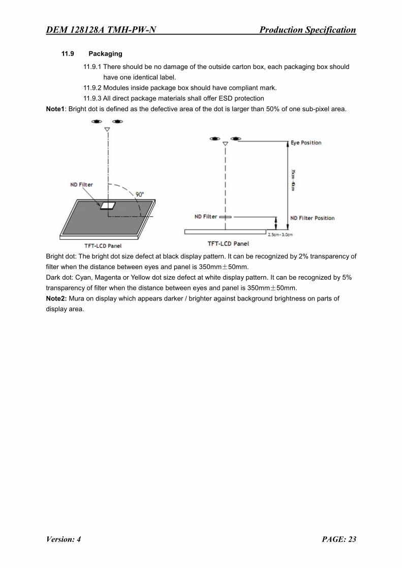
Note1: Bright dot is defined as the defective area of the dot is larger than 50% of one sub-pixel area.
Bright dot: The bright dot size defect at black display pattern. It can be recognized by 2% transparency of filter when the distance between eyes and panel is 350mm±50mm. Dark dot: Cyan, Magenta or Yellow dot size defect at white display pattern. It can be recognized by 5% transparency of filter when the distance between eyes and panel is 350mm±50mm. Note2: Mura on display which appears darker / brighter against background brightness on parts of display area.

DEM 128128A TMH-PW-N Production Specification
Version: 4 PAGE: 24
12. Reliability Specification
No Item Condition Quantity Criteria
1 High Temperature Operating 70℃, 96Hrs 2 GB/T2423.2 -2008
2 Low Temperature Operating -20℃, 96Hrs 2 GB/T2423.1 -2008
3 High Humidity 50℃, 90%RH, 96Hrs 2 GB/T2423.3 -2006
4 High Temperature Storage 80℃, 96Hrs 2 GB/T2423.2 -2008
5 Low Temperature Storage -30℃, 96Hrs 2 GB/T2423.1 -2008
6 Thermal Cycling Test -20℃, 60min~70℃, 60min, 20 cycles. 2 GB/T2423.22
-2012
7 Packing vibration Frequency range:10Hz~50Hz Acceleration of gravity:5G X, Y, Z 30 min for each direction.
2 GB/T5170.14 -2009
8 Electrical Static Discharge Air:±8KV 150pF/330Ω 5 times
2 GB/T17626.2 -2006 Contact:±4KV 150pF/330Ω 5 times
9 Drop Test (Packaged)
Height:80 cm,1 corner, 3 edges, 6 surfaces.
2 GB/T2423.8 -1995
Note1. No defection cosmetic and operational function allowable. Note2. Total current Consumption should be below double of initial value
DEM 128128A TMH-PW-N Production Specification
Version: 4 PAGE: 25
13. Precautions and Warranty
13.1 Safety
13.1.1 The liquid crystal in the LCD is poisonous. Do not put it in your mouth. If the liquid crystal touches your skin or clothes, wash it off immediately using soap and water. 13.1.2 Since the liquid crystal cells are made of glass, do not apply strong impact on them.
Handle with care.
13.2 Handling
13.2.1 Reverse and use within ratings in order to keep performance and prevent damage. 13.2.2 Do not wipe the polarizer with dry cloth, as it might cause scratch. If the surface of the LCD needs to be cleaned, wipe it swiftly with cotton or other soft cloth soaked with petroleum IPA, do not use other chemicals.
13.3 Storage
13.3.1 Do not store the LCD module beyond the specified temperature ranges.
13.4 Metal Pin (Apply to Products with Metal Pins)
13.4.1 Pins of LCD and Backlight 13.4.1.1 Solder tip can touch and press on the tip of Pin LEAD during the soldering 13.4.1.2 Recommended Soldering Conditions
Solder Type: Sn96.3~94-Ag3.3~4.3-Cu0.4~1.1 Maximum Solder Temperature: 370℃ Maximum Solder Time: 3s at the maximum temperature Recommended Soldering Temp: 350±20℃ Typical Soldering Time: ≤3s
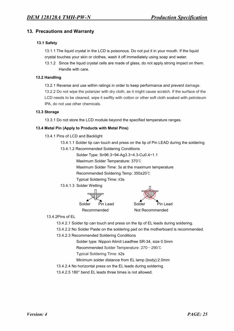
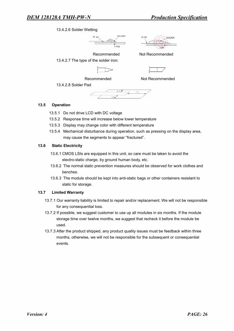
13.4.1.3 Solder Wetting
Solder Pin Lead Solder Pin Lead Recommended Not Recommended
13.4.2Pins of EL 13.4.2.1 Solder tip can touch and press on the tip of EL leads during soldering. 13.4.2.2 No Solder Paste on the soldering pad on the motherboard is recommended. 13.4.2.3 Recommended Soldering Conditions
Solder type: Nippon Alimit Leadfree SR-34, size 0.5mm Recommended Solder Temperature: 270~290℃ Typical Soldering Time: ≤2s
Minimum solder distance from EL lamp (body):2.0mm 13.4.2.4 No horizontal press on the EL leads during soldering. 13.4.2.5 180° bend EL leads three times is not allowed.
DEM 128128A TMH-PW-N Production Specification
Version: 4 PAGE: 26
13.4.2.6 Solder Wetting
Recommended Not Recommended
13.4.2.7 The type of the solder iron:
Recommended Not Recommended
13.4.2.8 Solder Pad
13.5 Operation
13.5.1 Do not drive LCD with DC voltage 13.5.2 Response time will increase below lower temperature 13.5.3 Display may change color with different temperature 13.5.4 Mechanical disturbance during operation, such as pressing on the display area,
may cause the segments to appear “fractured”.
13.6 Static Electricity
13.6.1 CMOS LSIs are equipped in this unit, so care must be taken to avoid the electro-static charge, by ground human body, etc.
13.6.2 The normal static prevention measures should be observed for work clothes and benches.
13.6.3 The module should be kept into anti-static bags or other containers resistant to static for storage.
13.7 Limited Warranty
13.7.1 Our warranty liability is limited to repair and/or replacement. We will not be responsible for any consequential loss.
13.7.2 If possible, we suggest customer to use up all modules in six months. If the module storage time over twelve months, we suggest that recheck it before the module be used.
13.7.3 After the product shipped, any product quality issues must be feedback within three months, otherwise, we will not be responsible for the subsequent or consequential events.
DEM 128128A TMH-PW-N Production Specification
Version: 4 PAGE: 27
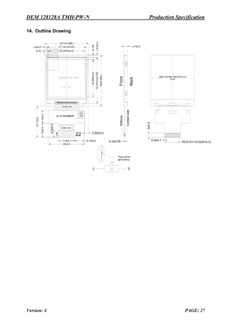
14. Outline Drawing
A K
30.7±0.2(BL)
25.4976(A.A)
2.7±0.227.7±0.2(LCD)
single area
36±0
.2(B
L)
26.4
96(A
.A)
32.2
4±0.
2(LC
D)
(3.1
8)
1.81
±0.2
(2.6)1.5±0.2
There will belight-leaking
Fron
t
Back
AK
single area
21.7
±0.5
10±0
.39±
0.2
11.5±0.125±0.3
6.75±0.2
2.85±0.3
0.3±0.05 P0.5*21=10.5(W=0.3)
3±0.
5
4.5±
0.5
0.5±0.1
1 22
Stif
fene
r
Con
tact
sid
e
UL E-NUMBER
DEM 128128A TMH-PW-N / EWYW