Embed Size (px)
Citation preview
1
DESIGN OF LOW NOISE AMPLIFIER
IN S-BAND
INTERNSHIP PROJECT REPORT
Submitted by
MYNAM HARIANTH
SC09B146
Communication Systems Group
ISRO SATELLITE CENTRE, BANGALORE
Department of Avionics
Indian Institute of Space Science and Technology
Thiruvananthapuram
June-July 2012
2
BONAFIDE CERTIFICATE
This is to certify that this project report titled DESIGN OF LOW NOISE
AMPLIFIER IN S-BAND submitted to Indian Institute of Space Science and
Technology, Thiruvananthapuram, is a bonafide record of work done by
Mr. MYNAM HARINATH under my supervision from JUNE 04th
2012 to
JULY 18th
2012.
Brijesh Kumar Soni
Sci. /Eng –SE
CMG
RAMA SUBRAMANIAN.R
DIVISION HEAD
CMG
Place : ISAC, Bangalore
Date :
3
Declaration by Author
This is to declare that this report has been written by me. No part of the report is plagiarized from
the other sources. All the information included from the other source has been mentioned in the
reference and acknowledged. I aver that if any part of the part of the report is found to be
plagiarized, I shall take full responsible for it.
(MYNAM HARINATH)
SC09B146
Place: ISAC, Bangalore
Date:
4
ABSTRACT
The following report presents the work done on the design simulation of low noise amplifier.
The purpose of amplifier is to amplify the received RF signals.
A brief description about how to approach for the designing of Low Noise Amplifier is discussed
here.
The main problem in designing an amplifier is which parameter we have to trade off to get other
one. How we can get low noise figure and stability by trading it with its system gain and vice
versa, is discussed here.
The criteria for choosing our substrate based on the required application and criteria for choosing
the device based on the requirements is discussed here.
There will be a lot of mathematical operations have to be done so I have chosen a simulation
environment, Advanced Design System (ADS). Using ADS simulation I have designed LNA for
optimal values of gain and noise figures.
5
ACKNOWLEDGEMENT
My first experiences of the project have been successful, thanks to the support staff
with gratitude. I wish to acknowledge all of them.
First of all I am very thankful to my project guide Mr. Brijesh Kumar Soni
under whose guideline I am able to complete my project. I am wholeheartedly
thankful to him for giving me his valuable time, attention and for providing me a
systematic way for completing my project in time.
I must make special mention of Mr. Rama Subramanian R our Division
Head for his co-operation.
I am also very thankful to Thomas Kurian sir our Dean and K.S. Das Gupta sir
our director who gave me an opportunity to present this project.
6
TABLE OF CONTENT
ABSTRACT………………………………………………………………………………. 4
ACKNOWLEDGEMENT………………………………………………………………... 5
CONTENTS……………………………………………………………………………… 6
ABRRIVATIONS………………………………………………………………………… 7
1. Introduction………………………………………................................................. 8
1.1 Methodology used …………………………………………………………… 9
1.2 Project Objective……………………............................................................... 9
2. RF Theory………………………………………………………………………… 10
2.1. Transmission Lines………………………………………………………….. 10
2.2. Selection of Substrate……………………………………………………….. 13
2.3. Devices………………………………………………………………………. 14
2.4. Power gains in Low noise amplifier…………………………………………. 17
2.5. Stability……………………………………………………………………… 21
2.6. Matching for maximum gain………………………………………………… 23
2.7. Noise in Microwave circuits…………………………………………………. 25
3. Designing of Low Noise Amplifier using ADS…………………………………. 27
3.1. Checking for Stability……………………………………………………….. 27
3.2. Minimizing the noise figure (First Stage)...…………………………… ……. 31
3.3. Maximizing the gain (Second Stage)………………………………………… 33
4. Final circuit of LNA……………………………….. ……………………………. 35
4.1. Two stage amplifier………………………………………………………….. 35
4.2. Layout of the LNA…………………………………………………………… 37
5. Results and Conclusion………………………………………………………….... 38
6. References………………………………………………………………………… 39
7
ABBRIVATIONS
NF, F NOISE FIGURE
LNA LOW NOISE AMPLIFIER
ADS ADVANCED NOISE FIGURE
MIC MICROWAVE INTEGRATED CIRCUITS
TEM TRANSVERSE ELECTROMAGNETIC
TE TRANSVERSE ELECTRIC
TM TRANSVERSE MAGNETIC
HBT HETRO JUNCTON BIPOLAR TRANSISTOR
HEMT HIGH ELECTRON MOBILITY TRANSISTOR
8
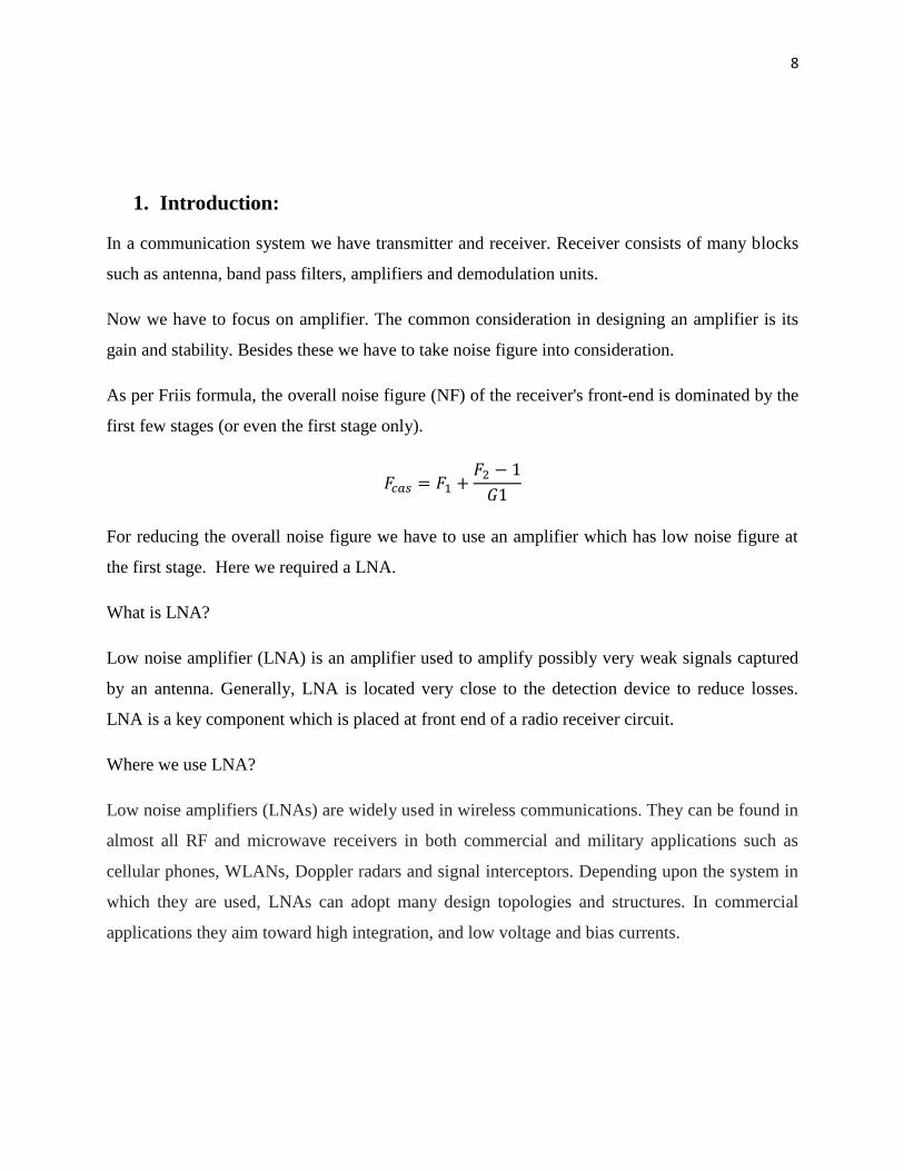
1. Introduction:
In a communication system we have transmitter and receiver. Receiver consists of many blocks
such as antenna, band pass filters, amplifiers and demodulation units.
Now we have to focus on amplifier. The common consideration in designing an amplifier is its
gain and stability. Besides these we have to take noise figure into consideration.
As per Friis formula, the overall noise figure (NF) of the receiver's front-end is dominated by the
first few stages (or even the first stage only).
For reducing the overall noise figure we have to use an amplifier which has low noise figure at
the first stage. Here we required a LNA.
What is LNA?
Low noise amplifier (LNA) is an amplifier used to amplify possibly very weak signals captured
by an antenna. Generally, LNA is located very close to the detection device to reduce losses.
LNA is a key component which is placed at front end of a radio receiver circuit.
Where we use LNA?
Low noise amplifiers (LNAs) are widely used in wireless communications. They can be found in
almost all RF and microwave receivers in both commercial and military applications such as
cellular phones, WLANs, Doppler radars and signal interceptors. Depending upon the system in
which they are used, LNAs can adopt many design topologies and structures. In commercial
applications they aim toward high integration, and low voltage and bias currents.
9
Why we use LNA?
LNAs are usually placed at the front-end of a receiver system, immediately following the
antenna. A band pass filter may be required in front of it if there are many adjacent interfering
bands leaking through the antenna, but this filter generally degrades the noise performance of the
system. The purpose of an LNA is to boost the desired signal power while adding as little noise
and distortion as possible so that retrieval of this signal is possible in the later stages in the
system.
1.1 Methodology used:
i. Choosing of the required substrate, device for the application.
ii. Learning the ADS simulation software used for designing the amplifier.
iii. Designing the amplifier based on the required specifications.
iv. Fitting the layout of the circuit in a given dimensions and adding biasing circuit to it.
1.2 Project Objective:
The main objective of our project is to design a LNA which has following specifications
Parameters Specifications
Operating frequency 2.1GHz
Gain(S(2,1)) Max gain possible (around 30dB)
Noise figure (NF) As minimum as possible(< 2.5dB)
S(1,1) < -10dB
S(2,2) < -15dB
Height of substrate 50mil
Relative permeability of substrate(εr) 10.5
104 Tanδ 1-20
10
2. RF Theory:
2.1 Transmission lines:
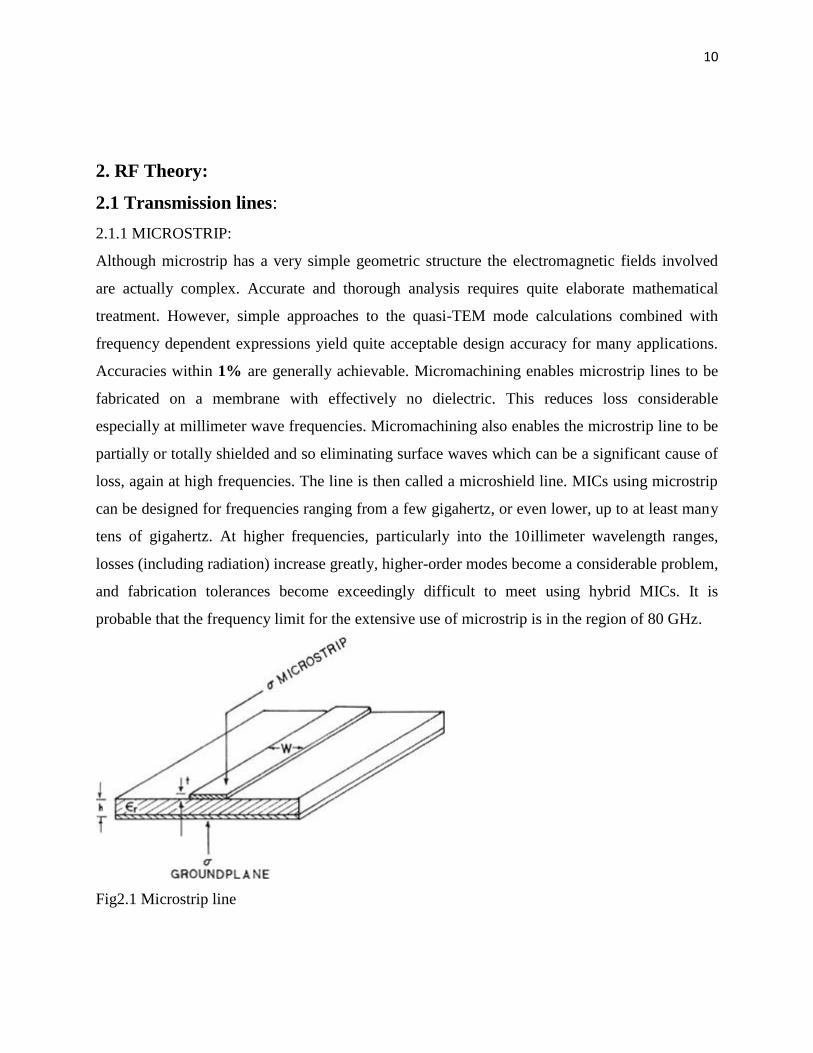
2.1.1 MICROSTRIP:
Although microstrip has a very simple geometric structure the electromagnetic fields involved
are actually complex. Accurate and thorough analysis requires quite elaborate mathematical
treatment. However, simple approaches to the quasi-TEM mode calculations combined with
frequency dependent expressions yield quite acceptable design accuracy for many applications.
Accuracies within 1% are generally achievable. Micromachining enables microstrip lines to be
fabricated on a membrane with effectively no dielectric. This reduces loss considerable
especially at millimeter wave frequencies. Micromachining also enables the microstrip line to be
partially or totally shielded and so eliminating surface waves which can be a significant cause of
loss, again at high frequencies. The line is then called a microshield line. MICs using microstrip
can be designed for frequencies ranging from a few gigahertz, or even lower, up to at least many
tens of gigahertz. At higher frequencies, particularly into the 10illimeter wavelength ranges,
losses (including radiation) increase greatly, higher-order modes become a considerable problem,
and fabrication tolerances become exceedingly difficult to meet using hybrid MICs. It is
probable that the frequency limit for the extensive use of microstrip is in the region of 80 GHz.
Fig2.1 Microstrip line
11
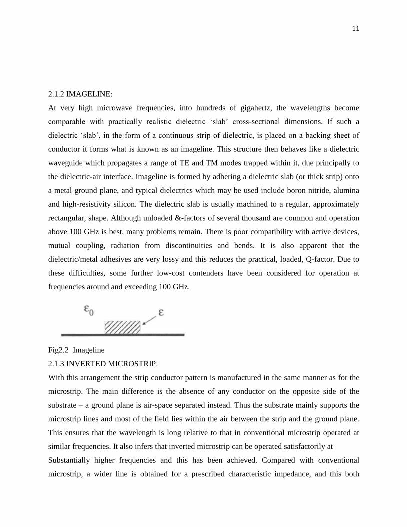
2.1.2 IMAGELINE:
At very high microwave frequencies, into hundreds of gigahertz, the wavelengths become
comparable with practically realistic dielectric ‘slab’ cross-sectional dimensions. If such a
dielectric ‘slab’, in the form of a continuous strip of dielectric, is placed on a backing sheet of
conductor it forms what is known as an imageline. This structure then behaves like a dielectric
waveguide which propagates a range of TE and TM modes trapped within it, due principally to
the dielectric-air interface. Imageline is formed by adhering a dielectric slab (or thick strip) onto
a metal ground plane, and typical dielectrics which may be used include boron nitride, alumina
and high-resistivity silicon. The dielectric slab is usually machined to a regular, approximately
rectangular, shape. Although unloaded &-factors of several thousand are common and operation
above 100 GHz is best, many problems remain. There is poor compatibility with active devices,
mutual coupling, radiation from discontinuities and bends. It is also apparent that the
dielectric/metal adhesives are very lossy and this reduces the practical, loaded, Q-factor. Due to
these difficulties, some further low-cost contenders have been considered for operation at
frequencies around and exceeding 100 GHz.
Fig2.2 Imageline
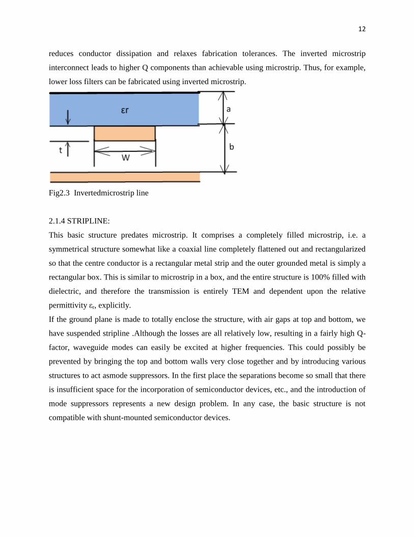
2.1.3 INVERTED MICROSTRIP:
With this arrangement the strip conductor pattern is manufactured in the same manner as for the
microstrip. The main difference is the absence of any conductor on the opposite side of the
substrate – a ground plane is air-space separated instead. Thus the substrate mainly supports the
microstrip lines and most of the field lies within the air between the strip and the ground plane.
This ensures that the wavelength is long relative to that in conventional microstrip operated at
similar frequencies. It also infers that inverted microstrip can be operated satisfactorily at
Substantially higher frequencies and this has been achieved. Compared with conventional
microstrip, a wider line is obtained for a prescribed characteristic impedance, and this both
12
reduces conductor dissipation and relaxes fabrication tolerances. The inverted microstrip
interconnect leads to higher Q components than achievable using microstrip. Thus, for example,
lower loss filters can be fabricated using inverted microstrip.
Fig2.3 Invertedmicrostrip line
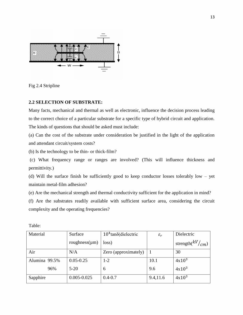
2.1.4 STRIPLINE:
This basic structure predates microstrip. It comprises a completely filled microstrip, i.e. a
symmetrical structure somewhat like a coaxial line completely flattened out and rectangularized
so that the centre conductor is a rectangular metal strip and the outer grounded metal is simply a
rectangular box. This is similar to microstrip in a box, and the entire structure is 100% filled with
dielectric, and therefore the transmission is entirely TEM and dependent upon the relative
permittivity εr, explicitly.
If the ground plane is made to totally enclose the structure, with air gaps at top and bottom, we
have suspended stripline .Although the losses are all relatively low, resulting in a fairly high Q-
factor, waveguide modes can easily be excited at higher frequencies. This could possibly be
prevented by bringing the top and bottom walls very close together and by introducing various
structures to act asmode suppressors. In the first place the separations become so small that there
is insufficient space for the incorporation of semiconductor devices, etc., and the introduction of
mode suppressors represents a new design problem. In any case, the basic structure is not
compatible with shunt-mounted semiconductor devices.
13
Fig 2.4 Stripline
2.2 SELECTION OF SUBSTRATE:
Many facts, mechanical and thermal as well as electronic, influence the decision process leading
to the correct choice of a particular substrate for a specific type of hybrid circuit and application.
The kinds of questions that should be asked must include:
(a) Can the cost of the substrate under consideration be justified in the light of the application
and attendant circuit/system costs?
(b) Is the technology to be thin- or thick-film?
(c) What frequency range or ranges are involved? (This will influence thickness and
permittivity.)
(d) Will the surface finish be sufficiently good to keep conductor losses tolerably low – yet
maintain metal-film adhesion?
(e) Are the mechanical strength and thermal conductivity sufficient for the application in mind?
(f) Are the substrates readily available with sufficient surface area, considering the circuit
complexity and the operating frequencies?
Table:
Material Surface
roughness(µm)
tanδ(dielectric
loss)
Dielectric
strength( ⁄ )
Air N/A Zero (approximately) 1 30
Alumina 99.5%
96%
0.05-0.25
5-20
1-2
6
10.1
9.6
4x
4x
Sapphire 0.005-0.025 0.4-0.7 9.4,11.6 4x
14
Quartz 0.006-0.025 1 3.8 10x
RT-Duroid 0.75-1 10-60 10.2-10.7 -
Si(high resistivity) 0.025 10-100 11.9 300
GaAs 0.025 6 12.85 350
2.3 Devices:
As devices aggressively scaled to reach ever higher operating frequencies, thinner base regions
and higher doping levels are required, which result in higher electric fields across narrow
depletion regions and give rise to significant leakage effects. As a result, conventional
technologies to define such thin, highly doped structures are being seriously stressed. More
specifically a number of features desirable for the realization of high frequency bipolar
transistors are conflicting. As an example, increasing the base and emitter doping concentrations
(to minimize the junction capacitance) actually reduces the device current gain, due to band gap
narrowing in the emitter and increased minority carrier injection from base to the emitter.
Bipolar technologies have embraced heterojunction strategies to great effect the additional
degree of freedom in engineering a device.
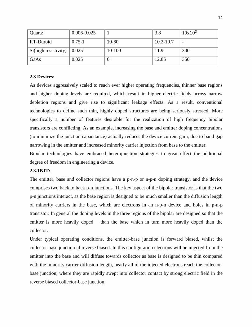
2.3.1BJT:
The emitter, base and collector regions have a p-n-p or n-p-n doping strategy, and the device
comprises two back to back p-n junctions. The key aspect of the bipolar transistor is that the two
p-n junctions interact, as the base region is designed to be much smaller than the diffusion length
of minority carriers in the base, which are electrons in an n-p-n device and holes in p-n-p
transistor. In general the doping levels in the three regions of the bipolar are designed so that the
emitter is more heavily doped than the base which in turn more heavily doped than the
collector.
Under typical operating conditions, the emitter-base junction is forward biased, whilst the
collector-base junction id reverse biased. In this configuration electrons will be injected from the
emitter into the base and will diffuse towards collector as base is designed to be thin compared
with the minority carrier diffusion length, nearly all of the injected electrons reach the collector-
base junction, where they are rapidly swept into collector contact by strong electric field in the
reverse biased collector-base junction.
15
Fig 2.5 Energy band diagram of BJT in forward bias.
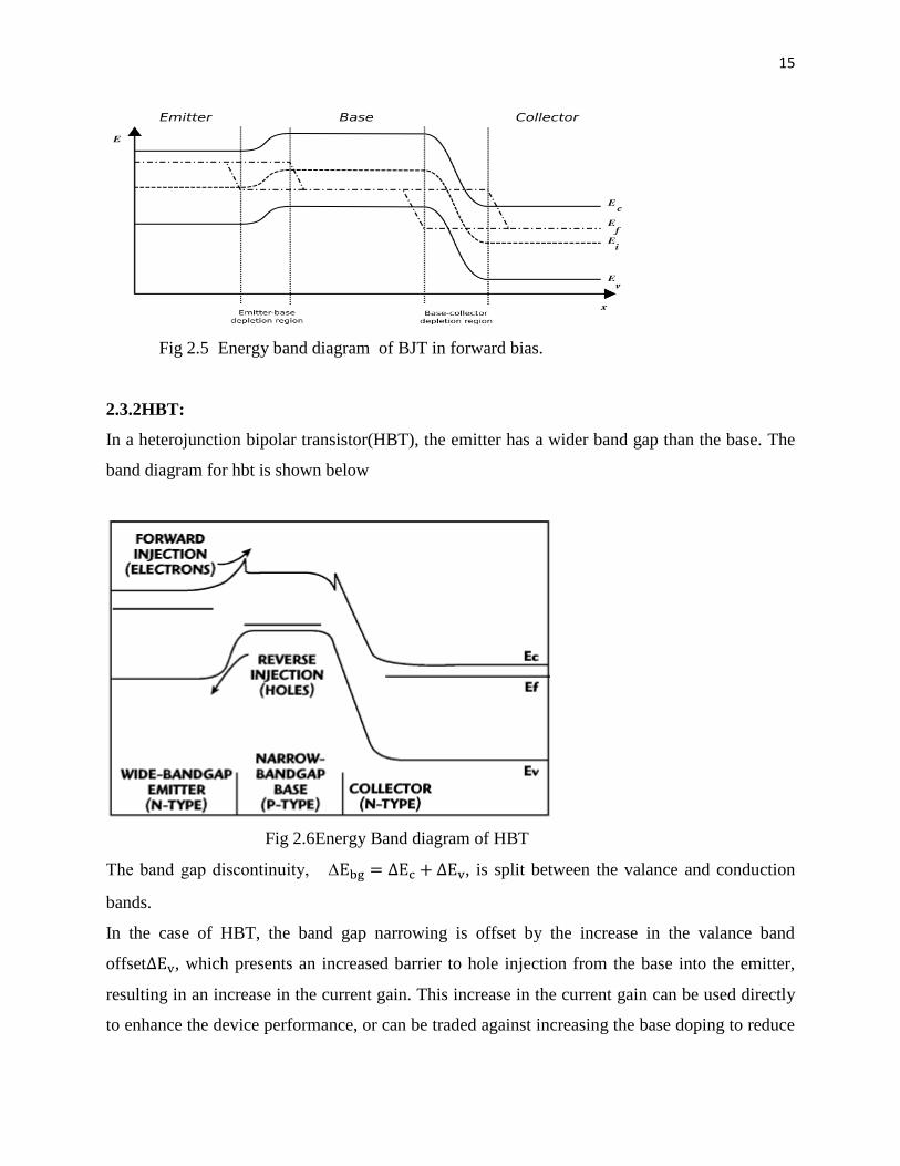
2.3.2HBT:
In a heterojunction bipolar transistor(HBT), the emitter has a wider band gap than the base. The
band diagram for hbt is shown below
Fig 2.6Energy Band diagram of HBT
The band gap discontinuity, ∆ , is split between the valance and conduction
bands.
In the case of HBT, the band gap narrowing is offset by the increase in the valance band
offset , which presents an increased barrier to hole injection from the base into the emitter,
resulting in an increase in the current gain. This increase in the current gain can be used directly
to enhance the device performance, or can be traded against increasing the base doping to reduce
16
base resistance, thus improving . As a further example, the conduction band offst at the
emitter-base junction means that the doping concentration of the emitter could be reduced, even
to a level below that of base, without compromising device operation. In this way, the emitter-
base capacitance can be reduced.
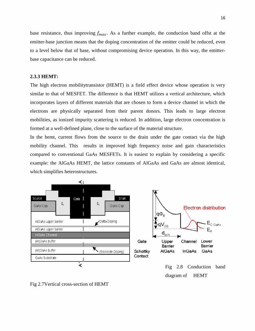
2.3.3 HEMT:
The high electron mobilitytransistor (HEMT) is a field effect device whose operation is very
similar to that of MESFET. The difference is that HEMT utilizes a vertical architecture, which
incorporates layers of different materials that are chosen to form a device channel in which the
electrons are physically separated from their parent donors. This leads to large electron
mobilities, as ionized impurity scattering is reduced. In addition, large electron concentration is
formed at a well-defined plane, close to the surface of the material structure.
In the hemt, current flows from the source to the drain under the gate contact via the high
mobility channel. This results in improved high frequency noise and gain characteristics
compared to conventional GaAs MESFETs. It is easiest to explain by considering a specific
example: the AlGaAs HEMT, the lattice constants of AlGaAs and GaAs are almost identical,
which simplifies heterostructures.
Fig 2.8 Conduction band
diagram of HEMT
Fig 2.7Vertical cross-section of HEMT
17
The doped GaAs cap facilitates the formation of low resistance ohmic contacts to the device. The
n-doped AlGaAs layer provides the electrons for the device channel, whilist the
undopedAlGaAs spacer layer is introduced to improve the channel mobility by spatially
separating the donor atoms from the electron accumulation layer. The aluminium concentration
determines the size of the conduction band discontinuity the AlGaAs/GaAs interface, which in
turn controls the concentration of the electron accumulation layer in the GaAs channel. The
larger the aluminium concentrations the larger the channel concentration.Aluminium
concentrations in the range 20-30% balance channel concentrations with mobility, which
decreases with aluminium concentration due to random alloy scattering. The high mobility
channel formed in the undopedGaAs channel layer results from the fact that AlGaAs has larger
bandgap than GaAs, and thus the electrons in the doped AlGaAs donar layer naturally
accumulate at the AlGaAs/GaAs interface as it is energetically favorable for them to reside in the
GaAs channel layer.
We have to choose a device based on the operating frequency, required gain and required noise
figure.
2.4 Power gains in Low noise amplifier:
Signal amplification is one of the most basic and prevalent circuit functions in modern RF and
microwave systems. For designing an amplifier we have to consider its gain and stability.
Now we are considering a general two port networks.
Fig 2.9 A two port network with arbitrary source and load impedances.
Consider an arbitrary two-port network, characterized by its scattering matrix, connectedto
source and load impedances and ..We will derive expressions for three types of power gain
18
in terms of the scattering parameters of the two-port network and the reflection coefficients,
and , of the source and load.
Power gain: G =
⁄ is the ratio of power dissipated in the load to thepower delivered to the
input of the two-port network. This gain is independent of , although the characteristics of
some active devices may be dependent on .
Available power gain: =
⁄ is the ratio of the power available from I-port network to
the power available from the source. This assumes conjugate matching of both the source and the
load, and depends on ,but not .
Transducer power gain : =
⁄ is the ratio of the power delivered to the load to the power
available from the source. This depends on both and
If the input and output are both conjugately matched to the two-port device then the gain is
maximized and G= = .
The reflection coefficient seen toward the load is
While the reflection coefficient seen toward source is
Where is the characteristic impedence.
We have
=
and
=
If peak values are assumed for all voltages, the average power delivered to the network is
| | | |
And power delivered to the load is
19
| | | |
The power gain can then be expressed as
The power available from the source, is the maximum power that can be delivered to the
network. This occurs when the input impedance of the terminated network is conjugately
matched to the source impedence, then
Similarly, the power available from the network, Pavn, is the maximum power that can be
delivered to the load, then
Pavs and Pavn have been expressed in terms of source voltage VS, which is independent of both
input or load impedences.
Then we obtain the available power gain as
The transducer power gain is
A special case of the transducer power gain occurs when both the input and output are matched
for zero reflection. Then ΓL= ΓS=0, and reduces
20
Another special case is the unilateral transducer power gain, GTU ,where S12=0,and ΓIN=S11 when
S12=0, so this gives the unilateral transducer power gain as
If the transducer is unilateral, so that S12=0, and Γin and Γout will become Γin=S11 and Γout=S22 and
the unilateral transducer gain reduces to GTU=GSG0GL, where
2.5 STABILITY:
Oscillations in the circuit is possible if either the input or output port impedence have a negative
real part, |Г in| > 1 or | Г out| > 1. Because |Г in| and |Г out | depends on source and load matching
networks. The stability of an amplifier depends on
ГS and ГL presented by matching networks. Thus we define two types of stability.
Unconditional stability: The network is unconditionally stable if |Г in| < 1 and |Г out| <
1for all passive source and load impedences.(i.e. |ГS |<1 and |ГL |<1).
Conditional stability: The network is conditionally stable if |Г in| > 1 or | Г out| > 1,
only for a certain range of passive source and load impedences.
Stability condition of an amplifier circuit is usually frequency dependent since the input
and output matching networks generally depend on frequency. It is therefore possible for
an amplifier to be stable at its design frequency but unstable at other frequencies.
21
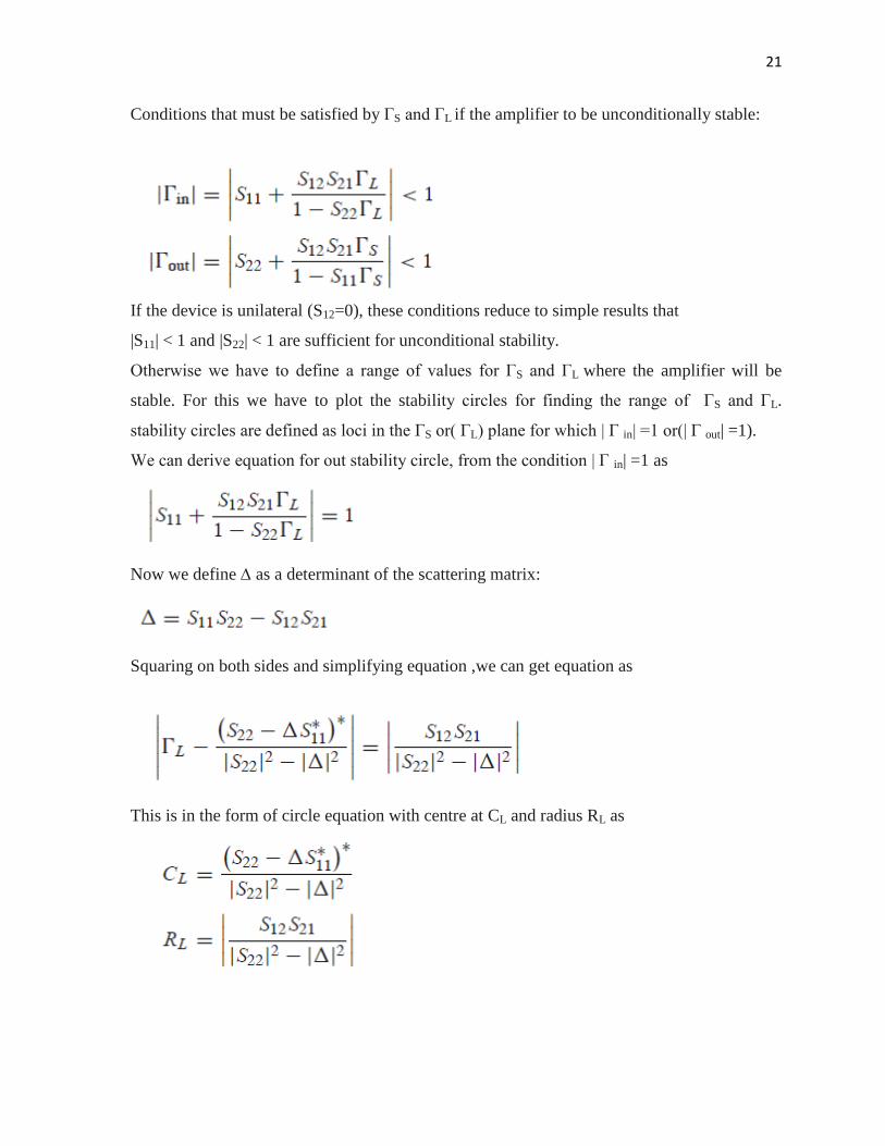
Conditions that must be satisfied by ГS and ГL if the amplifier to be unconditionally stable:
If the device is unilateral (S12=0), these conditions reduce to simple results that
|S11| < 1 and |S22| < 1 are sufficient for unconditional stability.
Otherwise we have to define a range of values for ГS and ГL where the amplifier will be
stable. For this we have to plot the stability circles for finding the range of ГS and ГL.
stability circles are defined as loci in the ГS or( ГL) plane for which | Г in| =1 or(| Г out| =1).
We can derive equation for out stability circle, from the condition | Г in| =1 as
Now we define as a determinant of the scattering matrix:
Squaring on both sides and simplifying equation ,we can get equation as
This is in the form of circle equation with centre at CL and radius RL as
22
For a given scattering matrix of transistor, we can plot input and output stability circles to
define where | Г in| =1 and | Г out| =1. On one side of input stability circle we will have | Г in| <
1 while on the other side we have | Г in| > 1.
If the device is unconditionally stable, the stability circles must be completely outside (or totally
enclose) the Smith chart. We can state this result mathematically as
Fig 2.10 For |S11| < 1. Fig 2.11 For |S11| > 1
Output stability circles for a conditionally stable
We have tests for checking unconditionally stability, K- test, where it can be shown that a
device will be unconditionally stable if Rollet’s condition, defined as
Along with the auxiliary condition that
are simultaneously satisfied these two conditions are necessary and sufficient conditions for
unconditionally stability, if the device scattering parameters do not satisfy the K- test, the
23
device is not unconditionally stable, and stability circles must be used to determine if there is any
values of ГS and ГL for which the device will be conditionally stable.\
K- test, is more mathematically rigorous for unconditional stability and it cannot be used for
relative stability of two or more devices.
We have another test involving only single parameter, defined as
Thus if >1 then the device is unconditionally stable. In addition we can say that larger values
of implies greater stability.
2.6 Designing for maximum Gain (Conjugate Matching):
After checking the stability of the transistor we have to match the circuit for maximum power
transfer.
Maximum power transfer from input matching network to the transistor will occur only when
Г in = ГS*, and maximum power transfer from transistor to output matching circuit only when
Г out = ГL*.
With assuming lossless matching circuit, these will maximize the overall transducer gain,
In addition with conjugate matching and losses matching sections, the input and output ports of
an amplifier are matched to Z0.
In general bilateral case Г in is effected by Г out. So input and output sections are matched
simultaneously by using
We can solve for ГS and ГL from the above
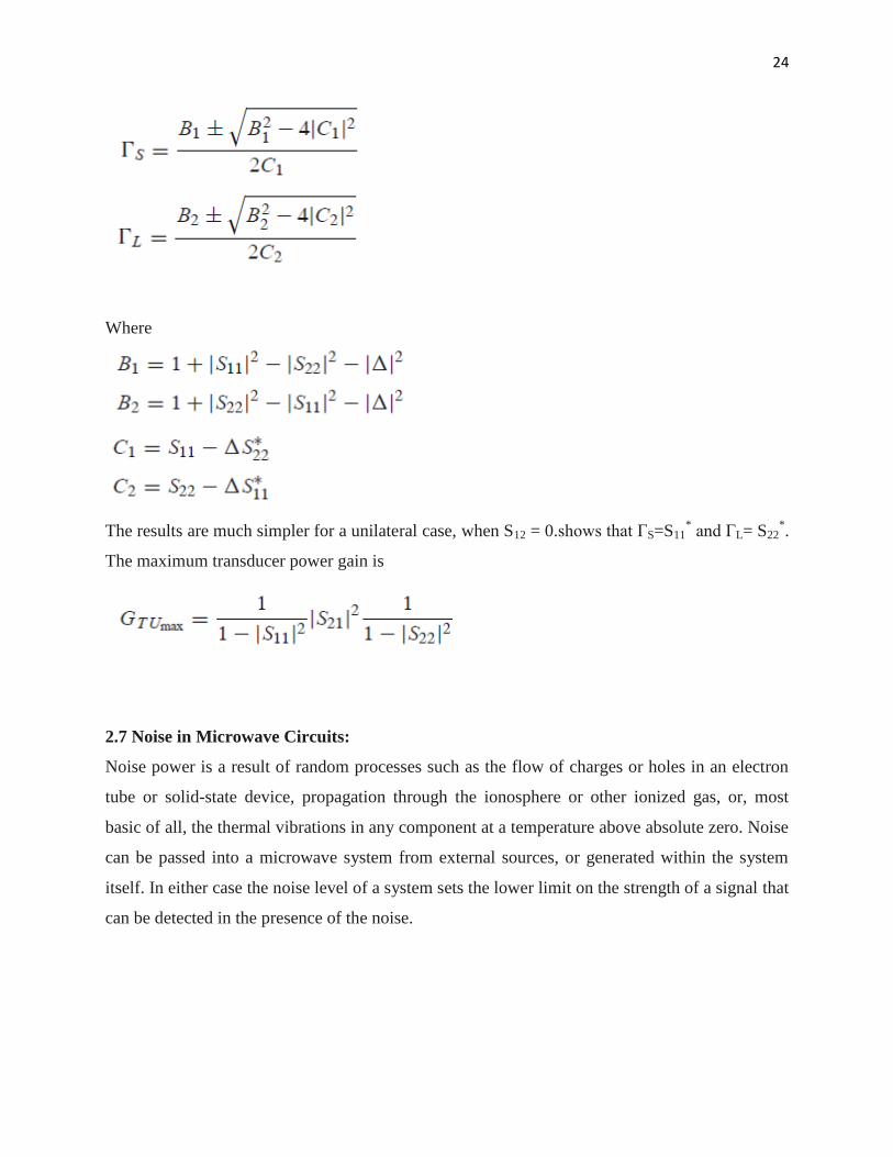
24
Where
The results are much simpler for a unilateral case, when S12 = 0.shows that ГS=S11* and ГL= S22
*.
The maximum transducer power gain is
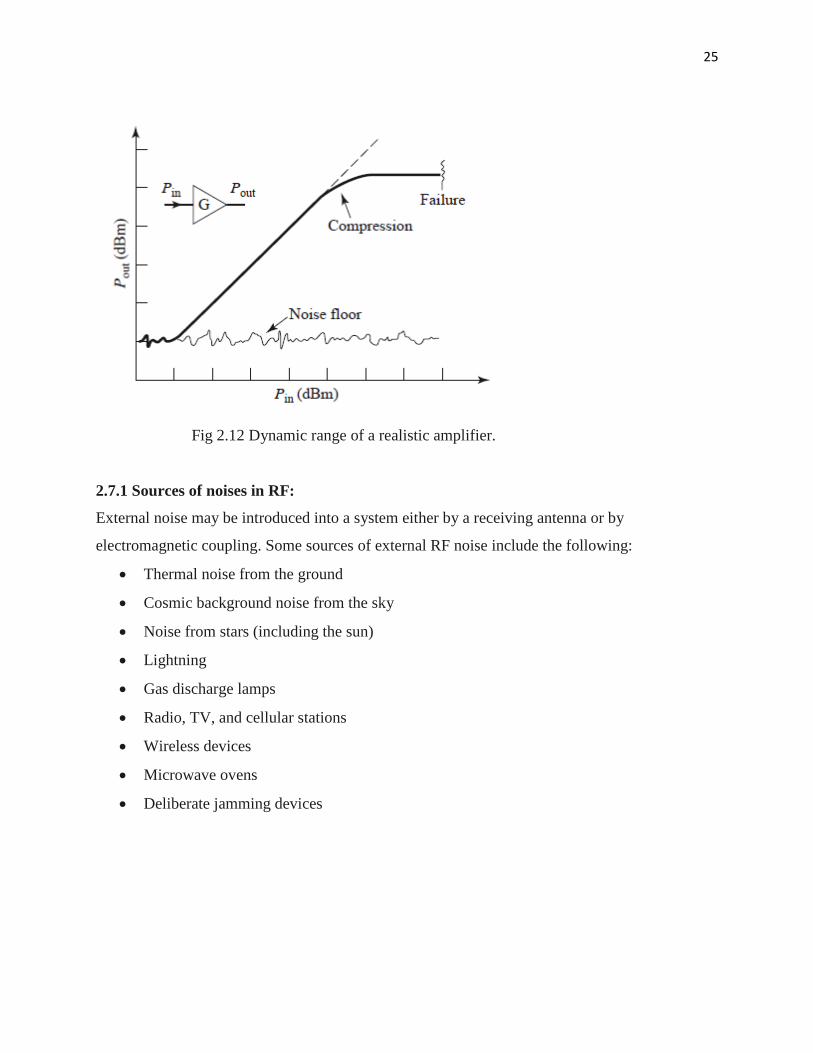
2.7 Noise in Microwave Circuits:
Noise power is a result of random processes such as the flow of charges or holes in an electron
tube or solid-state device, propagation through the ionosphere or other ionized gas, or, most
basic of all, the thermal vibrations in any component at a temperature above absolute zero. Noise
can be passed into a microwave system from external sources, or generated within the system
itself. In either case the noise level of a system sets the lower limit on the strength of a signal that
can be detected in the presence of the noise.
25
Fig 2.12 Dynamic range of a realistic amplifier.
2.7.1 Sources of noises in RF:
External noise may be introduced into a system either by a receiving antenna or by
electromagnetic coupling. Some sources of external RF noise include the following:
Thermal noise from the ground
Cosmic background noise from the sky
Noise from stars (including the sun)
Lightning
Gas discharge lamps
Radio, TV, and cellular stations
Wireless devices
Microwave ovens
Deliberate jamming devices
26
2.7.2 Noise figure:
The noise figure, F, is a measure of reduction in signal-to-noise ratio, and is defined as
Where Si, Ni are the input signal and noise powers and S0, N0 are the output signal and noise
powers.
Noise figure of cascaded system is
The noise figure of a two port amplifier can be expressed as
Where
The parameters Fmin, Гopt, and RN are characteristics of a particular transistor being used, are
called the noise parameters of a device.
We can give noise figure as
3. Designing of Low Noise Amplifier using ADS:
Now we have selected the substrate as RT-Duroid even tough sapphire is the best substrate, it
costs high so we have chosen alumina as our substrate and transmission line as microstrip line.
We selected device as HBT and all the other devices will work approximately same at our
desired frequency. (S-Band 2-4 GHz).
At first we have to check the stability of our device at the desired frequency using S-parameters.
27
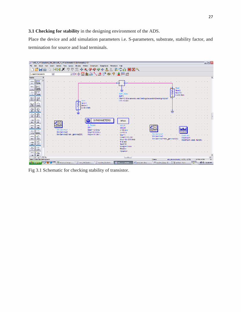
3.1 Checking for stability in the designing environment of the ADS.
Place the device and add simulation parameters i.e. S-parameters, substrate, stability factor, and
termination for source and load terminals.
Fig 3.1 Schematic for checking stability of transistor.
28
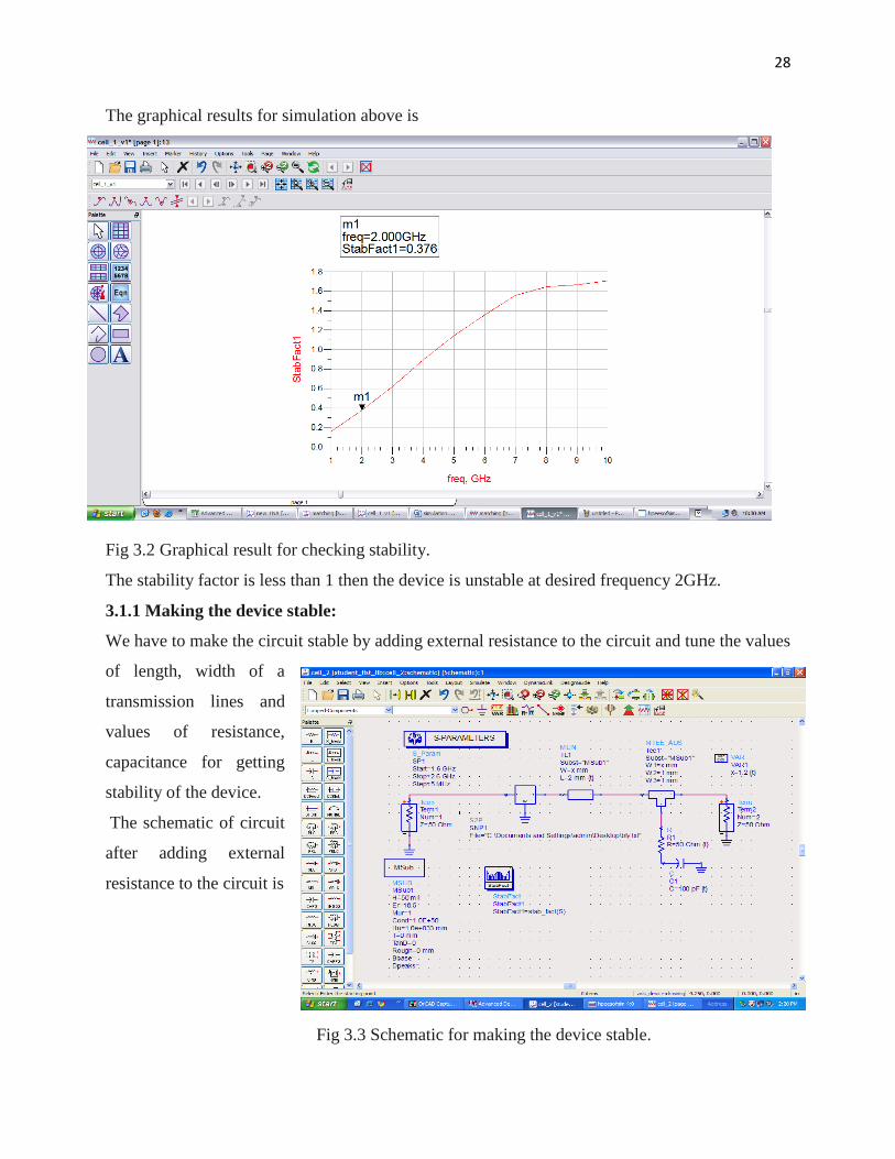
The graphical results for simulation above is
Fig 3.2 Graphical result for checking stability.
The stability factor is less than 1 then the device is unstable at desired frequency 2GHz.
3.1.1 Making the device stable:
We have to make the circuit stable by adding external resistance to the circuit and tune the values
of length, width of a
transmission lines and
values of resistance,
capacitance for getting
stability of the device.
The schematic of circuit
after adding external
resistance to the circuit is
Fig 3.3 Schematic for making the device stable.
29
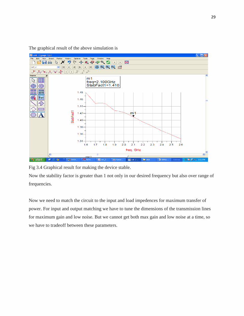
The graphical result of the above simulation is
Fig 3.4 Graphical result for making the device stable.
Now the stability factor is greater than 1 not only in our desired frequency but also over range of
frequencies.
Now we need to match the circuit to the input and load impedences for maximum transfer of
power. For input and output matching we have to tune the dimensions of the transmission lines
for maximum gain and low noise. But we cannot get both max gain and low noise at a time, so
we have to tradeoff between these parameters.
30
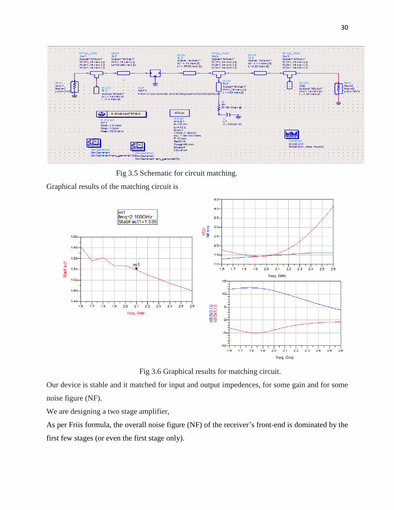
Fig 3.5 Schematic for circuit matching.
Graphical results of the matching circuit is
Fig 3.6 Graphical results for matching circuit.
Our device is stable and it matched for input and output impedences, for some gain and for some
noise figure (NF).
We are designing a two stage amplifier,
As per Friis formula, the overall noise figure (NF) of the receiver’s front-end is dominated by the
first few stages (or even the first stage only).
31
For reducing the overall noise figure we have make a minimum noise figure in the first stage.
And for the second stage we have to maximize the gain, for overall increase in gain of the circuit.
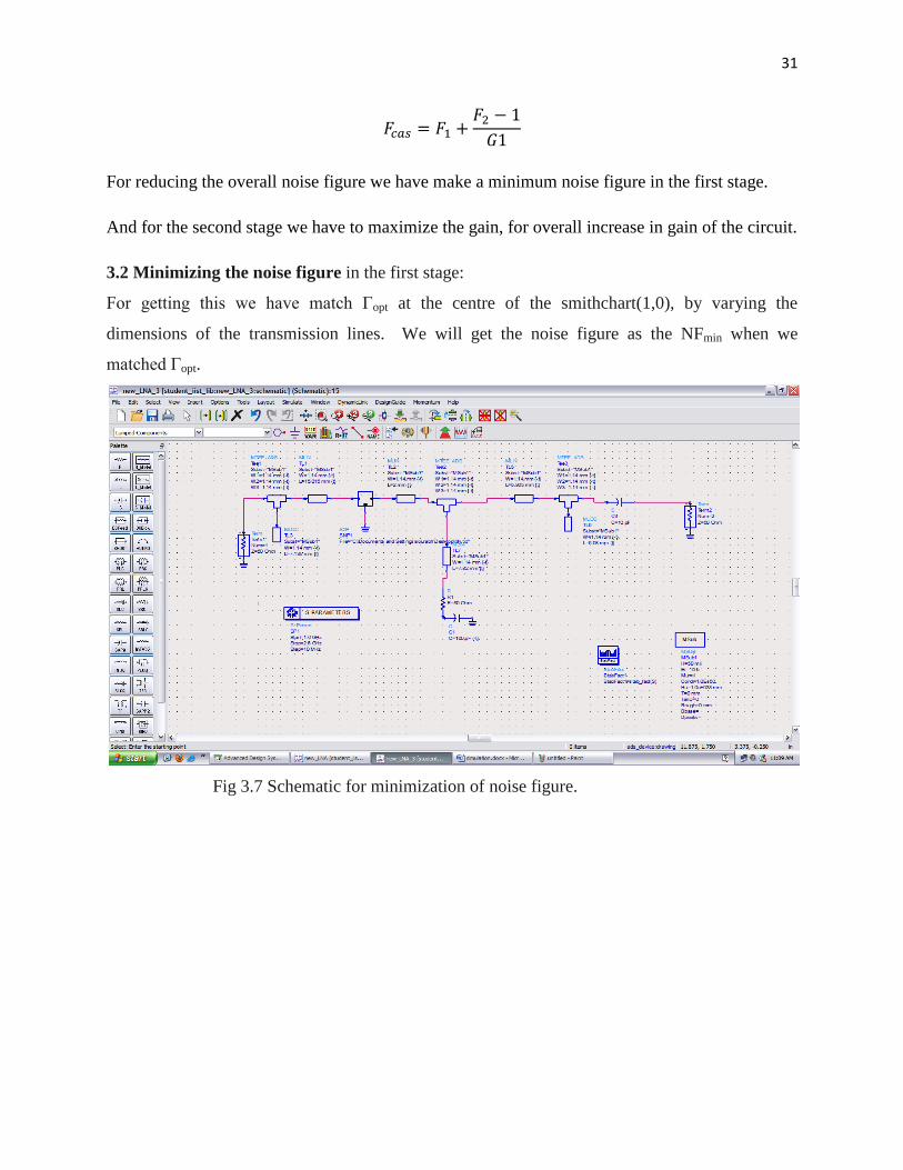
3.2 Minimizing the noise figure in the first stage:
For getting this we have match Гopt at the centre of the smithchart(1,0), by varying the
dimensions of the transmission lines. We will get the noise figure as the NFmin when we
matched Гopt.
Fig 3.7 Schematic for minimization of noise figure.
32
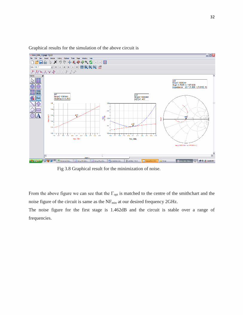
Graphical results for the simulation of the above circuit is
Fig 3.8 Graphical result for the minimization of noise.
From the above figure we can see that the Гopt is matched to the centre of the smithchart and the
noise figure of the circuit is same as the NFmin at our desired frequency 2GHz.
The noise figure for the first stage is 1.462dB and the circuit is stable over a range of
frequencies.
33
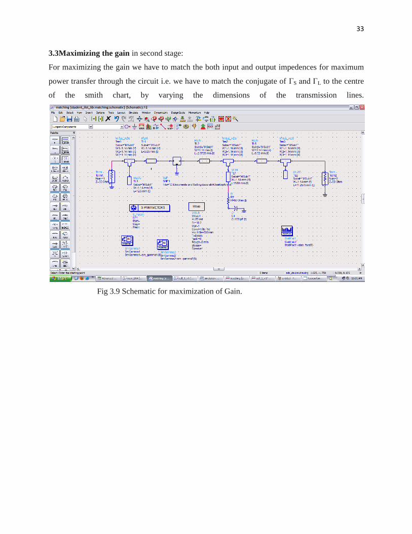
3.3Maximizing the gain in second stage:
For maximizing the gain we have to match the both input and output impedences for maximum
power transfer through the circuit i.e. we have to match the conjugate of ГS and ГL to the centre
of the smith chart, by varying the dimensions of the transmission lines.
Fig 3.9 Schematic for maximization of Gain.
34
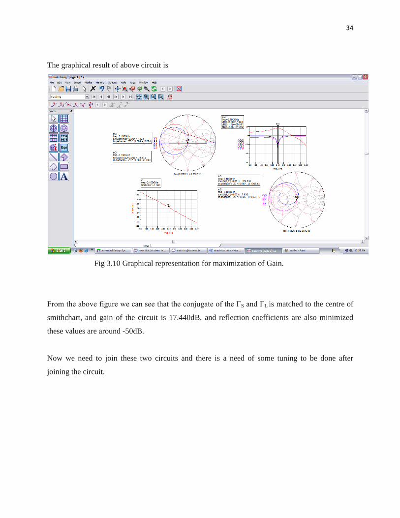
The graphical result of above circuit is
Fig 3.10 Graphical representation for maximization of Gain.
From the above figure we can see that the conjugate of the ГS and ГL is matched to the centre of
smithchart, and gain of the circuit is 17.440dB, and reflection coefficients are also minimized
these values are around -50dB.
Now we need to join these two circuits and there is a need of some tuning to be done after
joining the circuit.
35
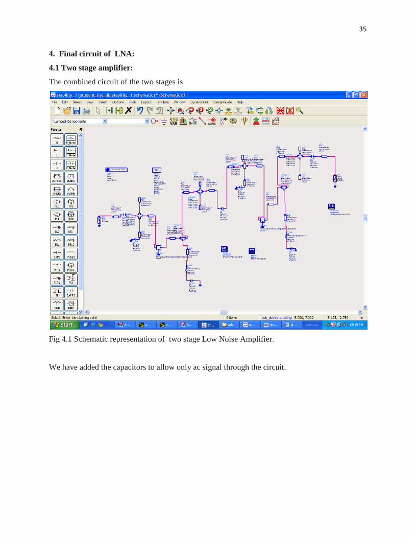
4. Final circuit of LNA:
4.1 Two stage amplifier:
The combined circuit of the two stages is
Fig 4.1 Schematic representation of two stage Low Noise Amplifier.
We have added the capacitors to allow only ac signal through the circuit.
36
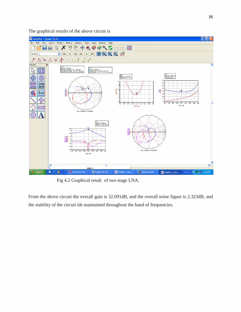
The graphical results of the above circuit is
Fig 4.2 Graphical result of two stage LNA.
From the above circuit the overall gain is 32.091dB, and the overall noise figure is 2.323dB, and
the stability of the circuit ids maintained throughout the band of frequencies.
37
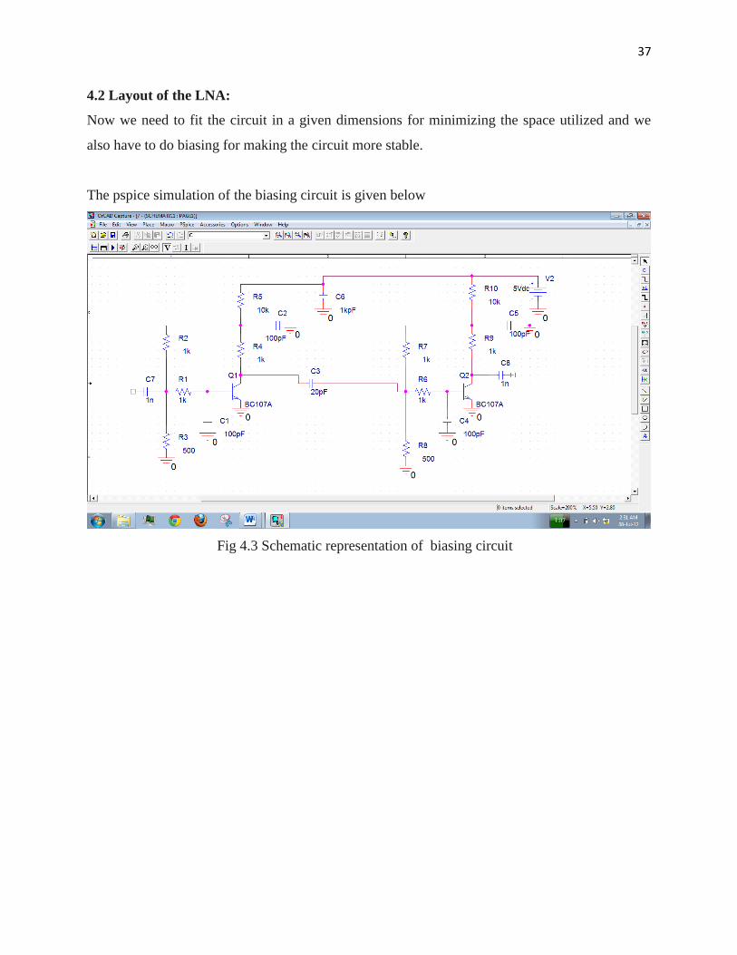
4.2 Layout of the LNA:
Now we need to fit the circuit in a given dimensions for minimizing the space utilized and we
also have to do biasing for making the circuit more stable.
The pspice simulation of the biasing circuit is given below
Fig 4.3 Schematic representation of biasing circuit
38
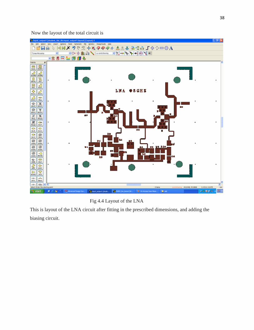
Now the layout of the total circuit is
Fig 4.4 Layout of the LNA
This is layout of the LNA circuit after fitting in the prescribed dimensions, and adding the
biasing circuit.
39
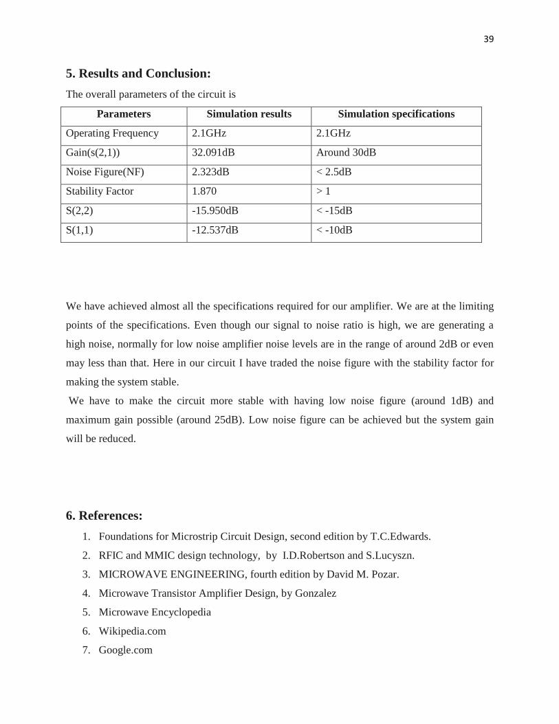
5. Results and Conclusion:
The overall parameters of the circuit is
Parameters Simulation results Simulation specifications
Operating Frequency 2.1GHz 2.1GHz
Gain(s(2,1)) 32.091dB Around 30dB
Noise Figure(NF) 2.323dB < 2.5dB
Stability Factor 1.870 > 1
S(2,2) -15.950dB < -15dB
S(1,1) -12.537dB < -10dB
We have achieved almost all the specifications required for our amplifier. We are at the limiting
points of the specifications. Even though our signal to noise ratio is high, we are generating a
high noise, normally for low noise amplifier noise levels are in the range of around 2dB or even
may less than that. Here in our circuit I have traded the noise figure with the stability factor for
making the system stable.
We have to make the circuit more stable with having low noise figure (around 1dB) and
maximum gain possible (around 25dB). Low noise figure can be achieved but the system gain
will be reduced.
6. References:
1. Foundations for Microstrip Circuit Design, second edition by T.C.Edwards.
2. RFIC and MMIC design technology, by I.D.Robertson and S.Lucyszn.
3. MICROWAVE ENGINEERING, fourth edition by David M. Pozar.
4. Microwave Transistor Amplifier Design, by Gonzalez
5. Microwave Encyclopedia
6. Wikipedia.com
7. Google.com


![RF Circuit Design - [Ch4-2] LNA, PA, and Broadband Amplifier](https://img.pdfslide.us/doc/110x75/55cf04aebb61eb002d8b45b4/rf-circuit-design-ch4-2-lna-pa-and-broadband-amplifier.jpg)