Embed Size (px)
Citation preview
LNA Design for Radio Navigation
Satellite System Receivers
Master of Science Thesis in the Master Degree Programme
Wireless and Photonics Engineering
ALEXANDRA ANDERSSON
Department of Microtechnology and Nanoscience
Division of Microwave Electronics Laboratory
CHALMERS UNIVERSITY OF TECHNOLOGY
Gothenburg, Sweden 2013

LNA Design for Radio Navigation Satellite
System Receivers
ALEXANDRA ANDERSSON
Department of Microtechnology and Nanoscience
Division of Microwave Electronics Laboratory
CHALMERS UNIVERSITY OF TECHNOLOGY
Gothenburg, Sweden 2013
LNA Design for Radio Navigation Satellite System Receivers
ALEXANDRA ANDERSSON
© ALEXANDRA ANDERSSON, 2013
Department of Microtechnology and Nanoscience
Chalmers University of Technology
SE-412 96 Gothenburg
Sweden
Telephone +46 (0)31-772 1000
Cover:
Photography of the complete LNA circuit, see section 5.5.
Chalmers Reproservice
Gothenburg, Sweden 2013
iii
LNA Design for Radio Navigation Satellite System Receivers
ALEXANDRA ANDERSSON
Department of Microtechnology and Nanoscience
Chalmers University of Technology
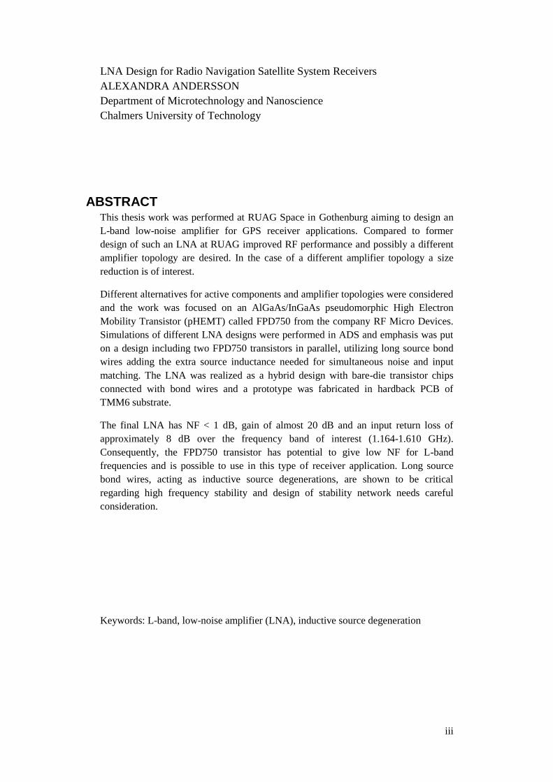
ABSTRACT This thesis work was performed at RUAG Space in Gothenburg aiming to design an
L-band low-noise amplifier for GPS receiver applications. Compared to former
design of such an LNA at RUAG improved RF performance and possibly a different
amplifier topology are desired. In the case of a different amplifier topology a size
reduction is of interest.
Different alternatives for active components and amplifier topologies were considered
and the work was focused on an AlGaAs/InGaAs pseudomorphic High Electron
Mobility Transistor (pHEMT) called FPD750 from the company RF Micro Devices.
Simulations of different LNA designs were performed in ADS and emphasis was put
on a design including two FPD750 transistors in parallel, utilizing long source bond
wires adding the extra source inductance needed for simultaneous noise and input
matching. The LNA was realized as a hybrid design with bare-die transistor chips
connected with bond wires and a prototype was fabricated in hardback PCB of
TMM6 substrate.
The final LNA has NF < 1 dB, gain of almost 20 dB and an input return loss of
approximately 8 dB over the frequency band of interest (1.164-1.610 GHz).
Consequently, the FPD750 transistor has potential to give low NF for L-band
frequencies and is possible to use in this type of receiver application. Long source
bond wires, acting as inductive source degenerations, are shown to be critical
regarding high frequency stability and design of stability network needs careful
consideration.
Keywords: L-band, low-noise amplifier (LNA), inductive source degeneration

iv
v
ACKNOWLEDGEMENTS Thanks to Robert Petersson at RUAG for giving me the opportunity to do this thesis
work. Also thanks to all of you at the department of Microwave Electronic Design at
RUAG for your support and encouragement. Especially thanks to Jonas Larsson for
being very helpful and patient with all my questions.

vi
vii
TABLE OF CONTENTS ABSTRACT .............................................................................................................................. iii
ACKNOWLEDGEMENTS ....................................................................................................... v
LIST OF ABBREVIATIONS ................................................................................................... ix
1 INTRODUCTION ............................................................................................................... 1
1.1 Background ................................................................................................................................ 1
1.2 Aim ............................................................................................................................................ 2
1.3 Approach to problem ................................................................................................................. 2
1.4 Thesis outline ............................................................................................................................. 2
2 LOW NOISE AMPLIFIER DESIGN.................................................................................. 3
2.1 Theory ........................................................................................................................................ 3
2.1.1 Noise figure ..................................................................................................................... 3
2.1.2 Input and output matching networks ............................................................................... 3
2.1.3 Conjugate match .............................................................................................................. 4
2.1.4 Stability ........................................................................................................................... 4
2.2 Classical LNA design techniques............................................................................................... 5
2.2.1 Classical noise matching (CNM) technique .................................................................... 5
2.2.2 Simultaneous noise and input matching (SNIM) technique ............................................ 5
2.2.3 Power-constrained noise optimization (PCNO) technique .............................................. 6
2.2.4 Power-constrained simultaneous noise and input matching (PCSNIM)
technique ......................................................................................................................................... 6
2.3 Broadband amplifier design ....................................................................................................... 6
2.4 Multi transistor amplifiers .......................................................................................................... 7
2.4.1 Transistors in parallel ...................................................................................................... 7
2.4.2 Transistors in cascade ...................................................................................................... 7
2.4.3 Transistors in cascode...................................................................................................... 8
3 FABRICATION TECHNOLOGIES ................................................................................... 9
3.1 Building practice ........................................................................................................................ 9
3.2 Choice of building practice, substrate and transistor ............................................................... 10
3.3 Chosen transistor ...................................................................................................................... 11
3.4 Benchmarks and comparison to other works ........................................................................... 11
4 INVESTIGATION OF AMPLIFIER TOPOLOGIES ...................................................... 13
4.1 Simulations of topologies and matching networks .................................................................. 13
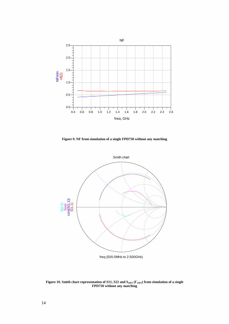
4.1.1 Characteristics of single transistor ................................................................................. 13
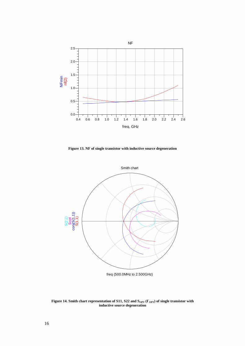
4.1.2 Single transistor with inductive source degeneration .................................................... 15
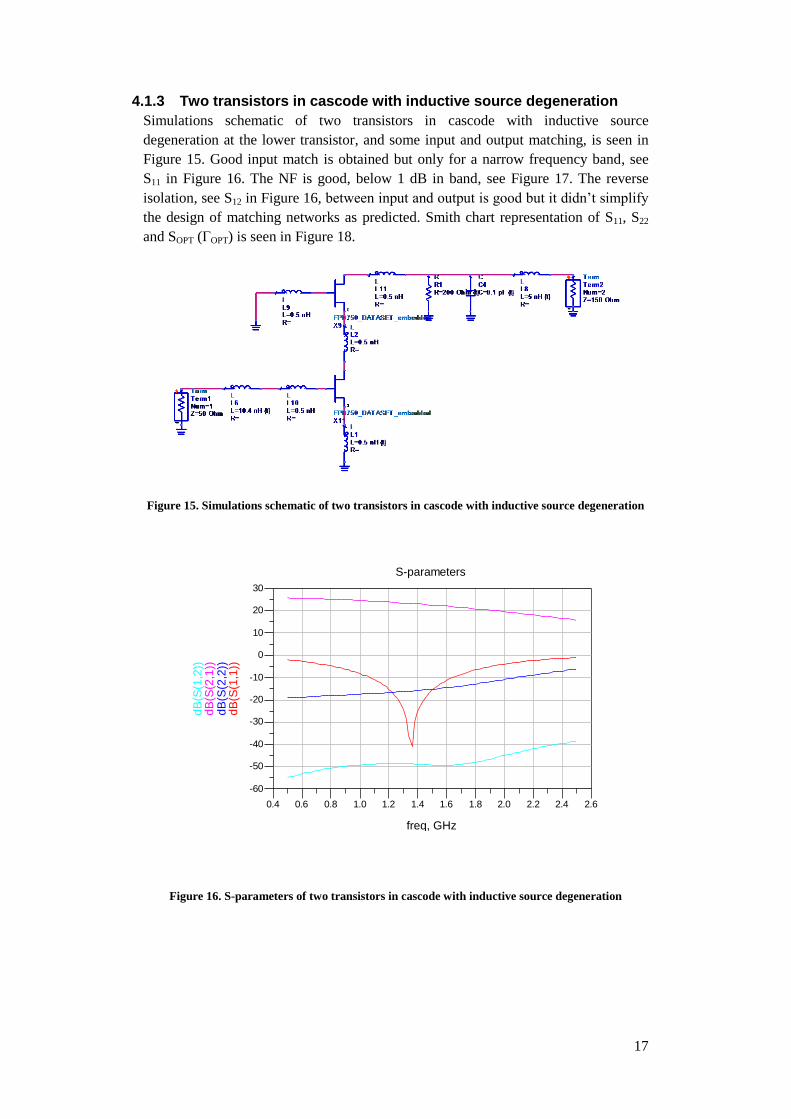
4.1.3 Two transistors in cascode with inductive source degeneration .................................... 17

viii
4.1.4 Two transistors with inductive source degeneration in parallel .................................... 20
4.1.5 Choice of topology ........................................................................................................ 22
5 DETAILED LNA DESIGN AND LAYOUT ................................................................... 23
5.1 Two transistors with inductive source degeneration in parallel ............................................... 23
5.1.1 Stability network ........................................................................................................... 23
5.1.2 De-embedding ............................................................................................................... 26
5.1.3 Input and output matching networks ............................................................................. 26
5.2 Simulated performance of the complete LNA ......................................................................... 29
5.3 Layout ...................................................................................................................................... 31
5.4 DC bias ..................................................................................................................................... 33
5.5 Fabrication and assembling ...................................................................................................... 34
5.6 Bond wire uncertainties ........................................................................................................... 36
6 MEASUREMENTS AND RESULTS............................................................................... 37
6.1 Bias tuning ............................................................................................................................... 37
6.2 RF measurements ..................................................................................................................... 38
6.2.1 Single transistor version ................................................................................................ 38
6.2.2 Dual transistor version ................................................................................................... 40
6.3 Comparison to existing balanced design .................................................................................. 42
7 CONCLUSIONS AND FUTURE WORK ........................................................................ 45
REFERENCES
APPENDIX A
APPENDIX B
APPENDIX C
ix
LIST OF ABBREVIATIONS
Abbreviation Description
GNSS Global Navigation Satellite System
LNA Low-noise amplifier
GPS Global Positioning System
RF Radio Frequency
MMIC Monolithic Microwave Integrated Circuit
pHEMT pseudomorphic High Electron Mobility Transistor
ADS Advanced Design System
LTCC Low temperature co-fired ceramic
VSWR Voltage standing wave ratio

x
1
1 INTRODUCTION The low-noise amplifier (LNA) is one of the most critical components determining
the sensitivity of a radio receiver. A particular challenge is the design of broadband
LNAs with simultaneously good noise figure (NF) and input return loss. An
application where broadband LNAs are required is in Global Navigation Satellite
System (GNSS) receivers.
1.1 Background GNSS is a collection of several satellite based navigation systems with global
coverage. The most familiar is probably the American GPS but it also contains
systems like the Russian GLONASS and the European Galileo. GNSS signals are
utilized by Radio occultation (RO) instruments in low Earth orbit (LEO) satellites.
RO is a remote sensing technique used for atmospheric sounding. It provides accurate
measurements from which vertical temperature profiles, pressure and humidity in the
atmosphere as well as profiles of electron content in the ionosphere can be derived.
GNSS RO has become an important tool in meteorology and climate monitoring
thanks to some key advantages: all-weather capability (not disturbed by clouds), high
vertical resolution, good accuracy of the retrieved temperature and long-term
consistency. [1]
In a simplified way a RO instrument in a LEO satellite works as follows. The
instrument acquires and tracks the GNSS signal at two frequencies, L1 and L2, above
the atmosphere. As the ray path descends into the atmosphere the Doppler shift (the
change in carrier phase) is recorded at the two frequencies. See Figure 1 for RO
geometry. [1]
Figure 1. Radio occultation geometry
Together with known spacecraft positions and velocities the Doppler shift provides
information on the directions of reception and transmission. Using the measurement
geometry and the spherically symmetric atmosphere condition the refraction index
profile as a function of the Earth radius is obtained from an integral transform (Abel
transform). The refractivity depends on the air pressure, temperature and water vapor
content. These parameters are then retrieved from the gas equation of state and the
2
hydrostatic equilibrium equation. In a similar approach the electron density profile
can be obtained from RO measurements in the ionosphere. [1] The instrument must
be able to track a sufficient number of GNSS satellites for RO and for usual real-time
navigation but it might also be equipped for precise orbit determination (POD) of the
LEO satellite itself.
At RUAG Space on-board receivers for this type of GNSS occultation and POD
instruments are developed. A receiver consists of several components such as
antenna, LNA, filters, mixer, local oscillator and power amplifier. An essential part is
the front-end, the LNA, since the noise contribution from the first component affects
the performance of the complete receiver.
1.2 Aim
This thesis work was performed at RUAG Space in Gothenburg aiming to design a
low-noise amplifier for GNSS receiver applications. Compared to existing design of
such an LNA at RUAG the objectives were:
Improved RF performance: focus on improved NF for maintained return loss
Reduced circuit size
The LNA needed to be stable and have sufficient gain. It was supposed to cover the
L-band (here referred to approximately 1.1-1.6 GHz). From design and fabrication
point of view also parameters as costs, mounting, interface, flexibility and time to
market needed to be considered.
1.3 Approach to problem RUAG’s existing LNA design for this GNSS receiver was studied together with
different alternatives for active components and amplifier topologies. After
considerations regarding RF performance, flexibility, time-to-market and costs it was
decided to continue the work focusing on an AlGaAs/InGaAs pseudomorphic High
Electron Mobility Transistor (pHEMT) called FPD750 from the company RF Micro
Devices. Using ADS a number of simulations were performed to investigate amplifier
topologies and configurations. Data from RF Micro Devices was used to model the
transistor. Emphasis was put on the most promising design and after optimizations
and layout work a breadboard (a prototype) was fabricated. Finally RF performance
of the complete circuit was measured and analyzed.
1.4 Thesis outline
The rest of this thesis is outlined as follows: Chapter 2 covers basic theory for design
of LNAs. Chapter 3 describes alternative technologies and choice of active
component is motivated. Chapter 4 discusses simulations performed in ADS to
analyze design alternatives for the chosen transistor. Chapter 5 presents detailed LNA
design and layout. Chapter 6 describes RF measurements and performance of the
breadboard. Chapter 7 includes conclusions and future work.
3
2 LOW NOISE AMPLIFIER DESIGN Typically the LNA is one of the key components as it tends to dominate the
sensitivity of the complete receiver. The received signal might be very weak and the
LNA is used to amplify the signal without adding too much noise from the LNA
itself. The LNA is usually placed close to the detection device (antenna) to reduce
losses and to avoid degradation of the signal-to-noise ratio (SNR). A good LNA adds
as little noise as possible to the signal and has high gain.
2.1 Theory
2.1.1 Noise figure
The noise of an amplifier can be described with a parameter called noise figure (NF).
NF is defined as the ratio of the available signal-to-noise power ratio at the input to
the available signal-to-noise power ratio at the output according to equation 1.
(1)
A minimum NF can be obtained by properly selecting the source reflection
coefficient (ΓS) of the amplifier, a method which is explained in following sections.
[2] The total NF for a chain of n cascaded amplifiers is
(2)
where GA is the available power gain. This shows that the noise contribution from the
first stage is significant for the complete amplifier performance. The objective when
designing LNAs is then to obtain low NF and high gain at the first amplifier stage.
Minimum NF and maximum power gain cannot be achieved simultaneously and
reflection coefficients have to be chosen as a compromise between noise and gain
performance.
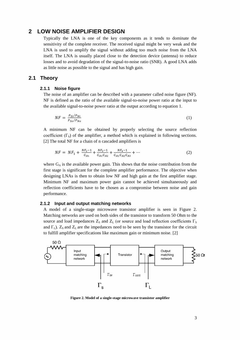
2.1.2 Input and output matching networks
A model of a single-stage microwave transistor amplifier is seen in Figure 2.
Matching networks are used on both sides of the transistor to transform 50 Ohm to the
source and load impedances ZS and ZL (or source and load reflection coefficients ΓS
and ΓL). ZS and ZL are the impedances need to be seen by the transistor for the circuit
to fulfill amplifier specifications like maximum gain or minimum noise. [2]
Figure 2. Model of a single-stage microwave transistor amplifier
4
2.1.3 Conjugate match
For a bilateral transistor (S12 ≠ 0) the input and output reflection coefficients are given
by
(3)
(4)
where S11, S12, S21 and S22 are the S-parameters of the transistor. For a unilateral
transistor (S12 = 0 or its effect is so small that it can be approximated to zero) the
input and output reflection coefficients are and .
Maximum transducer power gain is obtained by conjugate match and the source and
load reflection coefficients should be chosen as
(5)
and
(6)
See [2] for extended equations.
As most transistors appear as a significant impedance mismatch the frequency
response of the matching networks will be narrowband. This is an important aspect
for this project as the solution needs to be very wideband.
2.1.4 Stability
Stability is important to consider when designing microwave transistor amplifiers. If a
transistor is unconditionally stable it will not oscillate with any passive termination.
On the other hand a potentially unstable transistor can be stabilized by adding
resistive loadings. [2] One way of expressing necessary conditions for unconditional
stability is
(7)
and
(8)
where
(9)
and
(10)
Another alternative is to use the µ-factor where the condition µ > 1 alone is sufficient
for a circuit to be unconditionally stable. [3]
5
(11)
If the transistor is potentially unstable stability circles can be drawn in the Smith chart
to determine if there are values of ΓS and ΓL for which the transistor is conditionally
stable. [2]
2.2 Classical LNA design techniques
Designing LNAs involves tradeoffs between NF, gain, linearity, impedance matching
and power dissipation. The main goal is generally to design for simultaneous noise
and input impedance matching at any given amount of power dissipation. Four
common designing techniques are reviewed and analyzed in [4]. They are mentioned
as classical noise matching (CNM) technique, simultaneous noise and input matching
(SNIM) technique, power-constrained noise optimization (PCNO) technique and
power-constrained simultaneous noise and input matching (PCSNIM) technique.
2.2.1 Classical noise matching (CNM) technique
This method is based on designing the LNA for minimum NF by presenting the
optimum noise impedance ZOPT (or the optimum noise reflection coefficient ΓOPT) to
the given transistor. This is typically obtained by adding an input matching network
between the source and the input of the transistor. With this technique the amplifier
can be designed to have the lowest possible NF, Fmin, of the given transistor.
However, there can be a mismatch between ZOPT and ZIN* which is the desired input
matching network impedance for maximum gain. The amplifier might therefore
experience a significant gain mismatch at the input. As a result the CNM technique
requires compromise between gain and noise. [4]
2.2.2 Simultaneous noise and input matching (SNIM) technique
To achieve NF = Fmin of the amplifier the source reflection coefficient should be
chosen as ΓS = ΓOPT. In the same time, as described earlier, it is desirable to choose ΓS
= ΓIN* for maximum transducer power gain. Feedback is then a commonly used
technique to obtain both input matching and noise matching simultaneously when
designing LNA:s. With feedback the optimum noise impedance ZOPT can be shifted to
a desired point, in this case closer to the point of ZIN*. [4] This makes it possible to
choose a ΓS satisfying both noise and gain conditions simultaneously. Parallel
feedback is used for wide-band and improved input/output matching while series
feedback is preferred to obtain SNIM while causing no degradation of the NF. A
widely used series feedback technique is inductive source degeneration. It is applied
to common-source or cascode topologies and is done by adding an inductance LS in
series at the source of the transistor. [4]
For a small transistor size, hence for low power dissipation, and the LNA operating at
low frequencies it is not possible to achieve SNIM by adding inductive source
degeneration as the value of LS becomes too large and in the end instead increases the
minimum achievable NF. However, input matching can still be satisfied by proper
selection of LS as there exists an optimum transistor size that provides a minimum
NF. But this achievable minimum NF will be higher than Fmin of the original
common-source transistor. [4] This leads to the next topic, the PCNO technique.
6
2.2.3 Power-constrained noise optimization (PCNO) technique
As mentioned in the previous section the simultaneous gain and noise matching
approach can still be used for a constrained amount of power dissipation. For any
given amount of power dissipation, input matching can be obtained by proper
selection of LS for the given transistor size in combination with an input matching
circuit, typically a series inductance. For a fixed drain current and satisfied input
matching there exists a transistor size for which the NF of the amplifier is minimum.
However, this minimum NF is higher than Fmin of the original common-source
transistor due to the mismatch between ZS and ZOPT and/or the high value of LS which
can increase the minimum achievable NF. [4]
2.2.4 Power-constrained simultaneous noise and input matching (PCSNIM)
technique
For low-power applications, like for radio transceivers, SNIM and PCNO techniques
still don’t satisfy simultaneous noise and gain match. With an extended input
matching network, an additional capacitor, this can be solved and simultaneous
matching can be achieved for any amount of power dissipation. Limitations of this
technique are higher values of noise resistance (makes it less wide-band) and lower
effective cut-off frequency. [4]
2.3 Broadband amplifier design Designing broadband amplifiers requires careful considerations due to variations of
S-parameters, NF and VSWR with frequency. Two commonly used techniques when
designing broadband amplifiers are compensated matching networks and negative
feedback. Compensated matching networks involve mismatching the input and output
a bit to compensate for the variation of S21 with frequency. The networks are designed
for best input and output VSWR but it will only be optimum for certain frequencies in
the wide frequency band.
To achieve good input and output VSWR, gain flatness and low NF simultaneously
for a large bandwidth the use of balanced amplifiers is a practical method. This means
connecting two individual amplifiers by 3-dB hybrid couplers like Lange couplers or
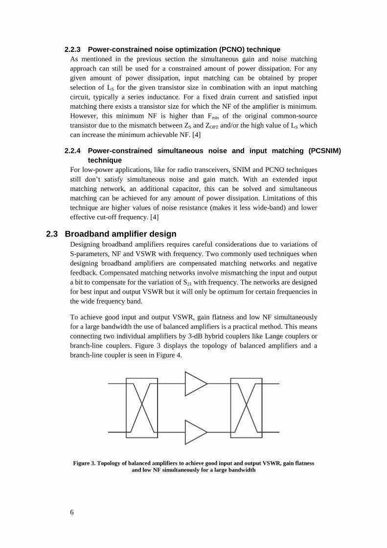
branch-line couplers. Figure 3 displays the topology of balanced amplifiers and a
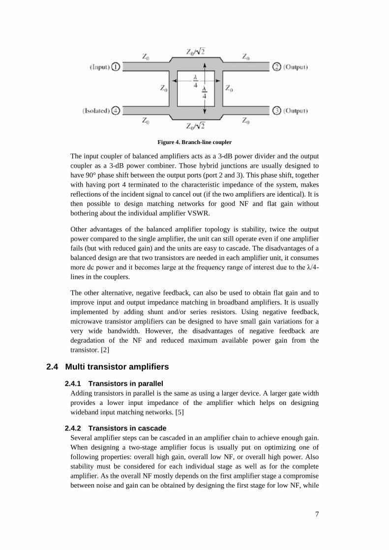
branch-line coupler is seen in Figure 4.
Figure 3. Topology of balanced amplifiers to achieve good input and output VSWR, gain flatness
and low NF simultaneously for a large bandwidth
7
Figure 4. Branch-line coupler
The input coupler of balanced amplifiers acts as a 3-dB power divider and the output
coupler as a 3-dB power combiner. Those hybrid junctions are usually designed to
have 90° phase shift between the output ports (port 2 and 3). This phase shift, together
with having port 4 terminated to the characteristic impedance of the system, makes
reflections of the incident signal to cancel out (if the two amplifiers are identical). It is
then possible to design matching networks for good NF and flat gain without
bothering about the individual amplifier VSWR.
Other advantages of the balanced amplifier topology is stability, twice the output
power compared to the single amplifier, the unit can still operate even if one amplifier
fails (but with reduced gain) and the units are easy to cascade. The disadvantages of a
balanced design are that two transistors are needed in each amplifier unit, it consumes
more dc power and it becomes large at the frequency range of interest due to the λ/4-
lines in the couplers.
The other alternative, negative feedback, can also be used to obtain flat gain and to
improve input and output impedance matching in broadband amplifiers. It is usually
implemented by adding shunt and/or series resistors. Using negative feedback,
microwave transistor amplifiers can be designed to have small gain variations for a
very wide bandwidth. However, the disadvantages of negative feedback are
degradation of the NF and reduced maximum available power gain from the
transistor. [2]
2.4 Multi transistor amplifiers
2.4.1 Transistors in parallel
Adding transistors in parallel is the same as using a larger device. A larger gate width
provides a lower input impedance of the amplifier which helps on designing
wideband input matching networks. [5]
2.4.2 Transistors in cascade
Several amplifier steps can be cascaded in an amplifier chain to achieve enough gain.
When designing a two-stage amplifier focus is usually put on optimizing one of
following properties: overall high gain, overall low NF, or overall high power. Also
stability must be considered for each individual stage as well as for the complete
amplifier. As the overall NF mostly depends on the first amplifier stage a compromise
between noise and gain can be obtained by designing the first stage for low NF, while
8
a higher NF is allowed in the second stage. Of course the first stage still needs to have
significant gain according to equation (2) to make use of the low NF. [2]
2.4.3 Transistors in cascode
When transistors are put in cascode one transistor operates as a common-source and
the other as a common-gate. It means that the drain of one transistor is connected to
the source of the other transistor. This improves the input-output isolation as there is
no direct coupling between the output and the input. The cascode topology is popular
due to advantages like large bandwidth, high gain and high reverse isolation. [4]
However, a drawback of this configuration compared to a simple common-source
amplifier is slightly higher noise figure. [6]
9
3 FABRICATION TECHNOLOGIES
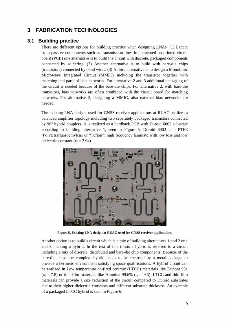
3.1 Building practice There are different options for building practice when designing LNAs. (1) Except
from passive components such as transmission lines implemented on printed circuit
board (PCB) one alternative is to build the circuit with discrete, packaged components
connected by soldering. (2) Another alternative is to build with bare-die chips
(transistors) connected by bond wires. (3) A third alternative is to design a Monolithic
Microwave Integrated Circuit (MMIC) including the transistor together with
matching and parts of bias networks. For alternative 2 and 3 additional packaging of
the circuit is needed because of the bare-die chips. For alternative 2, with bare-die
transistors, bias networks are often combined with the circuit board for matching
networks. For alternative 3, designing a MMIC, also external bias networks are
needed.
The existing LNA-design, used for GNSS receiver applications at RUAG, utilizes a
balanced amplifier topology including two separately packaged transistors connected
by 90° hybrid couplers. It is realized as a hardback PCB with Duroid 6002 substrate
according to building alternative 1, seen in Figure 5. Duroid 6002 is a PTFE
(Polytetrafluoroethylene or “Teflon”) high frequency laminate with low loss and low
dielectric constant (εr = 2.94).
Figure 5. Existing LNA-design at RUAG used for GNSS receiver applications
Another option is to build a circuit which is a mix of building alternatives 1 and 2 or 1
and 3, making a hybrid. In the rest of this thesis a hybrid is referred to a circuit
including a mix of discrete, distributed and bare-die chip components. Because of the
bare-die chips the complete hybrid needs to be enclosed by a metal package to
provide a hermetic environment satisfying space qualifications. A hybrid circuit can
be realized in Low temperature co-fired ceramic (LTCC) materials like Dupont 951
(εr = 7.8) or thin film materials like Alumina 99.6% (εr = 9.5). LTCC and thin film
materials can provide a size reduction of the circuit compared to Duroid substrates
due to their higher dielectric constants and different substrate thickness. An example
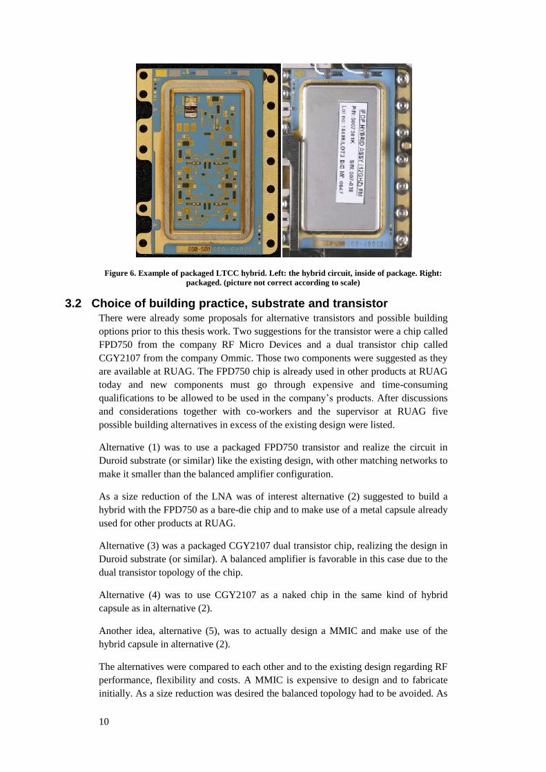
of a packaged LTCC hybrid is seen in Figure 6.
10
Figure 6. Example of packaged LTCC hybrid. Left: the hybrid circuit, inside of package. Right:
packaged. (picture not correct according to scale)
3.2 Choice of building practice, substrate and transistor There were already some proposals for alternative transistors and possible building
options prior to this thesis work. Two suggestions for the transistor were a chip called
FPD750 from the company RF Micro Devices and a dual transistor chip called
CGY2107 from the company Ommic. Those two components were suggested as they
are available at RUAG. The FPD750 chip is already used in other products at RUAG
today and new components must go through expensive and time-consuming
qualifications to be allowed to be used in the company’s products. After discussions
and considerations together with co-workers and the supervisor at RUAG five
possible building alternatives in excess of the existing design were listed.
Alternative (1) was to use a packaged FPD750 transistor and realize the circuit in
Duroid substrate (or similar) like the existing design, with other matching networks to
make it smaller than the balanced amplifier configuration.
As a size reduction of the LNA was of interest alternative (2) suggested to build a
hybrid with the FPD750 as a bare-die chip and to make use of a metal capsule already
used for other products at RUAG.
Alternative (3) was a packaged CGY2107 dual transistor chip, realizing the design in
Duroid substrate (or similar). A balanced amplifier is favorable in this case due to the
dual transistor topology of the chip.
Alternative (4) was to use CGY2107 as a naked chip in the same kind of hybrid
capsule as in alternative (2).
Another idea, alternative (5), was to actually design a MMIC and make use of the
hybrid capsule in alternative (2).
The alternatives were compared to each other and to the existing design regarding RF
performance, flexibility and costs. A MMIC is expensive to design and to fabricate
initially. As a size reduction was desired the balanced topology had to be avoided. As
11
the dual transistor chip from Ommic preferably is used in a balanced design, to
actually utilize the advantage of having two transistors in the same chip, it was also
discarded. It was decided that this work was about to progress with focus on the
FPD750 transistor used as a bare-die chip, realizing the LNA as a hybrid design. For
breadboard fabrication high frequency laminates called TMM6 (εr = 6) and TMM10
(εr = 9.20) can be used to mimic LTCC and thin film materials. Only TMM6 material
was available at RUAG at the moment and it was chosen as substrate for breadboard
fabrication of the LNA.
3.3 Chosen transistor FPD750 is an AlGaAs/InGaAs 0.5 Watt power pHEMT. It is preferably used in
power amplifiers but at relatively low frequencies, such as the L-band, it is probably
applicable also in LNAs. An objective of the prospective work was to determine if
this actually is suitable. Except from being a practical choice as an existing
component at RUAG, another advantage of this transistor is that it tolerates high input
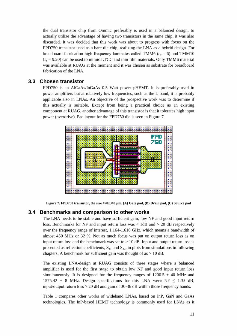
power (overdrive). Pad layout for the FPD750 die is seen in Figure 7.
Figure 7. FPD750 transistor, die size 470x340 µm. (A) Gate pad, (B) Drain pad, (C) Source pad
3.4 Benchmarks and comparison to other works The LNA needs to be stable and have sufficient gain, low NF and good input return
loss. Benchmarks for NF and input return loss was < 1dB and > 20 dB respectively
over the frequency range of interest, 1.164-1.610 GHz, which means a bandwidth of
almost 450 MHz or 32 %. Not as much focus was put on output return loss as on
input return loss and the benchmark was set to > 10 dB. Input and output return loss is
presented as reflection coefficients, S11 and S22, in plots from simulations in following
chapters. A benchmark for sufficient gain was thought of as > 10 dB.
The existing LNA-design at RUAG consists of three stages where a balanced
amplifier is used for the first stage to obtain low NF and good input return loss
simultaneously. It is designed for the frequency ranges of 1200.5 ± 40 MHz and
1575.42 ± 8 MHz. Design specifications for this LNA were NF ≤ 1.35 dB,
input/output return loss ≥ 20 dB and gain of 30-36 dB within those frequency bands.
Table 1 compares other works of wideband LNAs, based on InP, GaN and GaAs
technologies. The InP-based HEMT technology is commonly used for LNAs as it
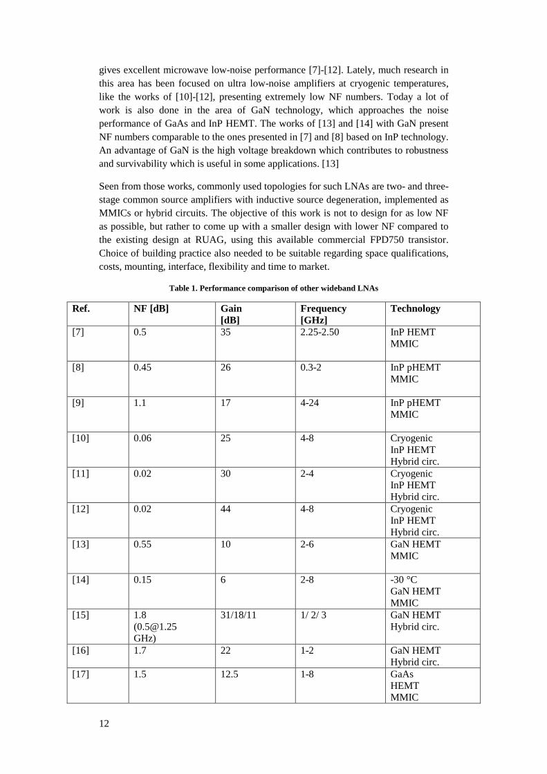
12
gives excellent microwave low-noise performance [7]-[12]. Lately, much research in
this area has been focused on ultra low-noise amplifiers at cryogenic temperatures,
like the works of [10]-[12], presenting extremely low NF numbers. Today a lot of
work is also done in the area of GaN technology, which approaches the noise
performance of GaAs and InP HEMT. The works of [13] and [14] with GaN present
NF numbers comparable to the ones presented in [7] and [8] based on InP technology.
An advantage of GaN is the high voltage breakdown which contributes to robustness
and survivability which is useful in some applications. [13]
Seen from those works, commonly used topologies for such LNAs are two- and three-
stage common source amplifiers with inductive source degeneration, implemented as
MMICs or hybrid circuits. The objective of this work is not to design for as low NF
as possible, but rather to come up with a smaller design with lower NF compared to
the existing design at RUAG, using this available commercial FPD750 transistor.
Choice of building practice also needed to be suitable regarding space qualifications,
costs, mounting, interface, flexibility and time to market.
Table 1. Performance comparison of other wideband LNAs
Ref. NF [dB] Gain
[dB]
Frequency
[GHz]
Technology
[7] 0.5 35 2.25-2.50 InP HEMT
MMIC
[8] 0.45 26 0.3-2 InP pHEMT
MMIC
[9] 1.1 17 4-24 InP pHEMT
MMIC
[10] 0.06 25 4-8 Cryogenic
InP HEMT
Hybrid circ.
[11] 0.02
30 2-4 Cryogenic
InP HEMT
Hybrid circ.
[12] 0.02
44 4-8 Cryogenic
InP HEMT
Hybrid circ.
[13] 0.55
10 2-6
GaN HEMT
MMIC
[14] 0.15 6 2-8 -30 °C
GaN HEMT
MMIC
[15] 1.8
GHz)
31/18/11 1/ 2/ 3 GaN HEMT
Hybrid circ.
[16] 1.7 22 1-2 GaN HEMT
Hybrid circ.
[17] 1.5 12.5 1-8 GaAs
HEMT
MMIC
13
4 INVESTIGATION OF AMPLIFIER TOPOLOGIES As it was of interest to avoid a balanced amplifier other designs had to be considered.
Different configurations and simple matching networks were simulated using ADS to
see if there was any topology more advantageous than the others. Analyzed
topologies were a single transistor, putting two transistors in cascode or in parallel
and with or without inductive source degeneration. Available FPD750 transistor data,
from RF Micro Devices, are S-parameters and noise parameters measured up to 6
GHz for a packaged transistor chip and S-parameters measured up to 26.5 GHz for a
bare-die transistor chip. The available data was measured for a DC bias of Vd=3.3 V
and Id=50 mA.
4.1 Simulations of topologies and matching networks To start with the data file with S-parameters and noise parameters measured up to 6
GHz was used to plot S-parameters, Fmin and NF for a single transistor and later for
the different topologies and simple matching networks. Only ideal component models
were used for inductances and capacitors in the matching networks at this point.
4.1.1 Characteristics of single transistor
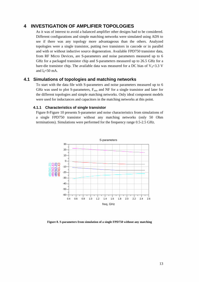
Figure 8-Figure 10 presents S-parameter and noise characteristics from simulations of
a single FPD750 transistor without any matching networks (only 50 Ohm
terminations). Simulations were performed for the frequency range 0.5-2.5 GHz.
Figure 8. S-parameters from simulation of a single FPD750 without any matching
0.6 0.8 1.0 1.2 1.4 1.6 1.8 2.0 2.2 2.40.4 2.6
-50
-40
-30
-20
-10
0
10
20
-60
30
freq, GHz
dB
(S(1
,1))
dB
(S(2
,2))
dB
(S(2
,1))
dB
(S(1
,2))
S-parameters
14
Figure 9. NF from simulation of a single FPD750 without any matching
Figure 10. Smith chart representation of S11, S22 and SOPT (ΓOPT) from simulation of a single
FPD750 without any matching
0.6 0.8 1.0 1.2 1.4 1.6 1.8 2.0 2.2 2.40.4 2.6
0.5
1.0
1.5
2.0
0.0
2.5
freq, GHz
nf(
2)
NF
min
NF
freq (500.0MHz to 2.500GHz)
S(1
,1)
co
nj(S
(1,1
))S
op
tS
(2,2
)
Smith chart
15
4.1.2 Single transistor with inductive source degeneration
Simulations schematic for a single transistor with inductive source degeneration and
input and output matching networks is seen in Figure 11. With inductive source
degeneration curves for S11* (= ΓIN* if S12 is approximated to zero) and SOPT (ΓOPT)
come closer to each other, seen in the smith chart plot in Figure 14. The NF is good,
see Figure 13, but despite matching networks at input and output the specifications on
S11 and S22 are still not fulfilled in the complete L-band, see Figure 12.
Figure 11. Simulations schematic of single transistor with inductive source degeneration
Figure 12. S-parameters of single transistor with inductive source degeneration
0.6 0.8 1.0 1.2 1.4 1.6 1.8 2.0 2.2 2.40.4 2.6
-50
-40
-30
-20
-10
0
10
20
-60
30
freq, GHz
dB
(S(1
,1))
dB
(S(2
,2))
dB
(S(2
,1))
dB
(S(1
,2))
S-parameters
16
Figure 13. NF of single transistor with inductive source degeneration
Figure 14. Smith chart representation of S11, S22 and SOPT (ΓOPT) of single transistor with
inductive source degeneration
0.6 0.8 1.0 1.2 1.4 1.6 1.8 2.0 2.2 2.40.4 2.6
0.5
1.0
1.5
2.0
0.0
2.5
freq, GHz
nf(
2)
NF
min
NF
freq (500.0MHz to 2.500GHz)
S(1
,1)
co
nj(S
(1,1
))S
op
tS
(2,2
)
Smith chart
17
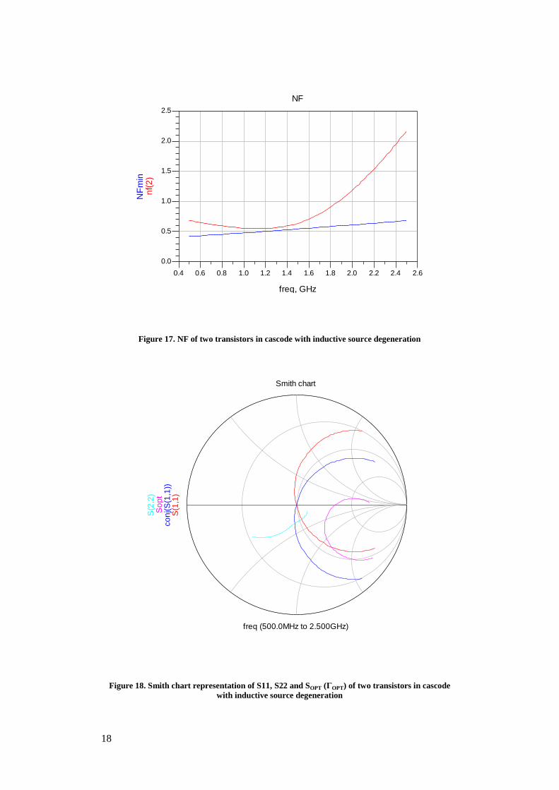
4.1.3 Two transistors in cascode with inductive source degeneration
Simulations schematic of two transistors in cascode with inductive source
degeneration at the lower transistor, and some input and output matching, is seen in
Figure 15. Good input match is obtained but only for a narrow frequency band, see
S11 in Figure 16. The NF is good, below 1 dB in band, see Figure 17. The reverse
isolation, see S12 in Figure 16, between input and output is good but it didn’t simplify
the design of matching networks as predicted. Smith chart representation of S11, S22
and SOPT (ΓOPT) is seen in Figure 18.
Figure 15. Simulations schematic of two transistors in cascode with inductive source degeneration
Figure 16. S-parameters of two transistors in cascode with inductive source degeneration
0.6 0.8 1.0 1.2 1.4 1.6 1.8 2.0 2.2 2.40.4 2.6
-50
-40
-30
-20
-10
0
10
20
-60
30
freq, GHz
dB
(S(1
,1))
dB
(S(2
,2))
dB
(S(2
,1))
dB
(S(1
,2))
S-parameters
18
Figure 17. NF of two transistors in cascode with inductive source degeneration
Figure 18. Smith chart representation of S11, S22 and SOPT (ΓOPT) of two transistors in cascode
with inductive source degeneration
0.6 0.8 1.0 1.2 1.4 1.6 1.8 2.0 2.2 2.40.4 2.6
0.5
1.0
1.5
2.0
0.0
2.5
freq, GHz
nf(
2)
NF
min
NF
freq (500.0MHz to 2.500GHz)
S(1
,1)
co
nj(S
(1,1
))S
op
tS
(2,2
)
Smith chart
19
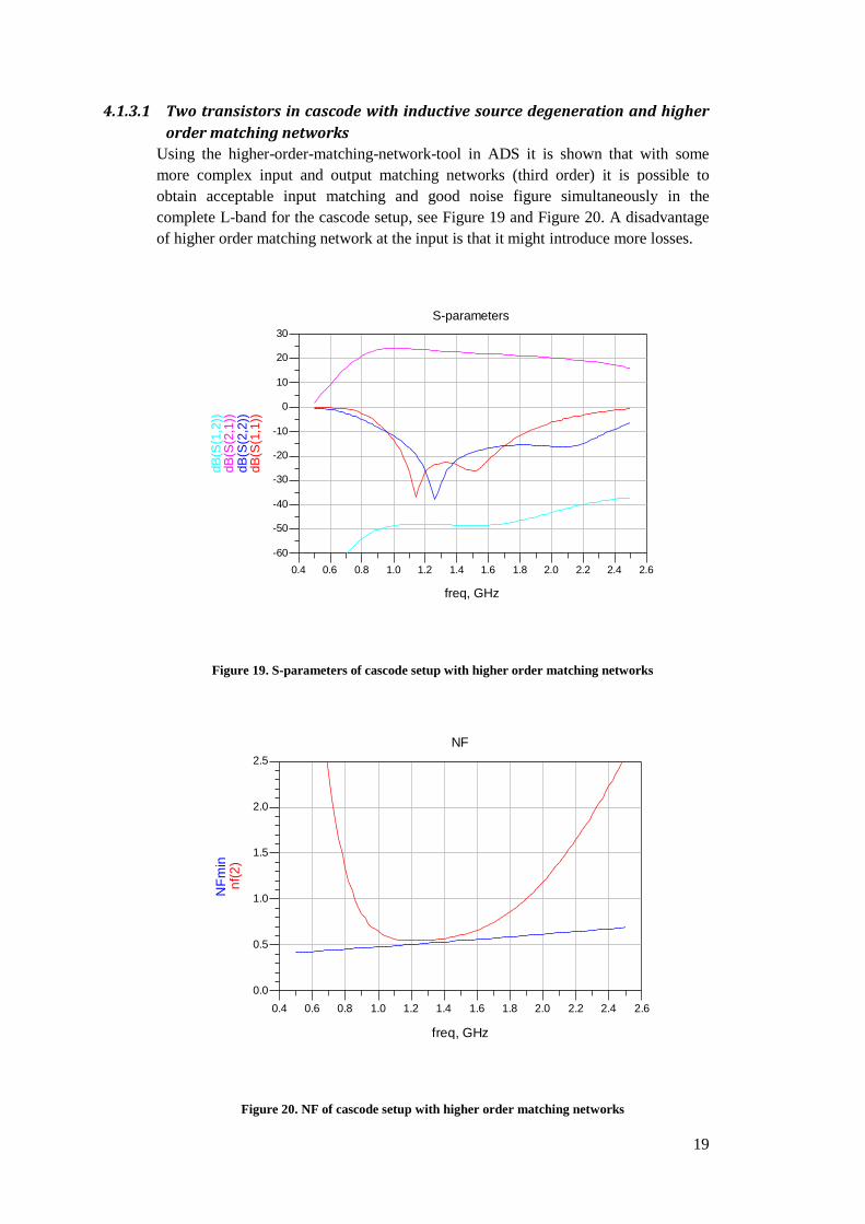
4.1.3.1 Two transistors in cascode with inductive source degeneration and higher
order matching networks
Using the higher-order-matching-network-tool in ADS it is shown that with some
more complex input and output matching networks (third order) it is possible to
obtain acceptable input matching and good noise figure simultaneously in the
complete L-band for the cascode setup, see Figure 19 and Figure 20. A disadvantage
of higher order matching network at the input is that it might introduce more losses.
Figure 19. S-parameters of cascode setup with higher order matching networks
Figure 20. NF of cascode setup with higher order matching networks
0.6 0.8 1.0 1.2 1.4 1.6 1.8 2.0 2.2 2.40.4 2.6
-50
-40
-30
-20
-10
0
10
20
-60
30
freq, GHz
dB
(S(1
,1))
dB
(S(2
,2))
dB
(S(2
,1))
dB
(S(1
,2))
S-parameters
0.6 0.8 1.0 1.2 1.4 1.6 1.8 2.0 2.2 2.40.4 2.6
0.5
1.0
1.5
2.0
0.0
2.5
freq, GHz
nf(
2)
NF
min
NF
20
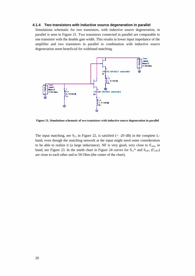
4.1.4 Two transistors with inductive source degeneration in parallel
Simulations schematic for two transistors, with inductive source degeneration, in
parallel is seen in Figure 21. Two transistors connected in parallel are comparable to
one transistor with the double gate width. This results in lower input impedance of the
amplifier and two transistors in parallel in combination with inductive source
degeneration seem beneficial for wideband matching.
Figure 21. Simulations schematic of two transistors with inductive source degeneration in parallel
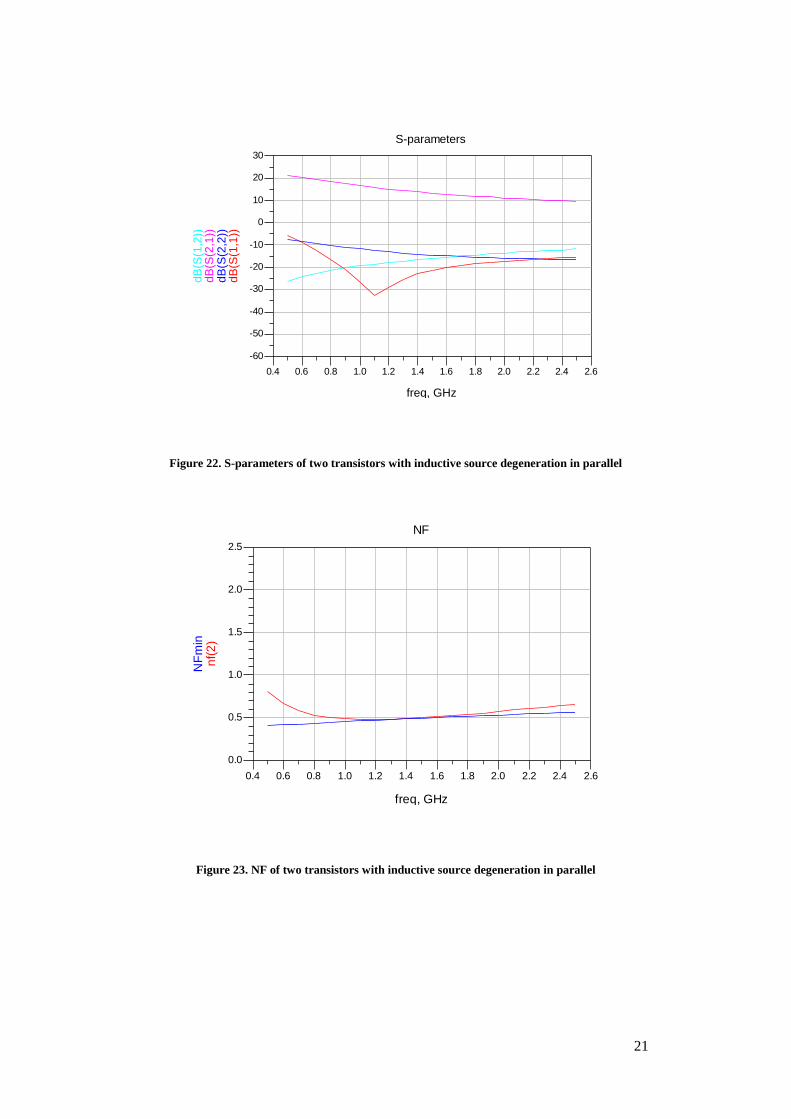
The input matching, see S11 in Figure 22, is satisfied (< -20 dB) in the complete L-
band, even though the matching network at the input might need some consideration
to be able to realize it (a large inductance). NF is very good, very close to Fmin, in
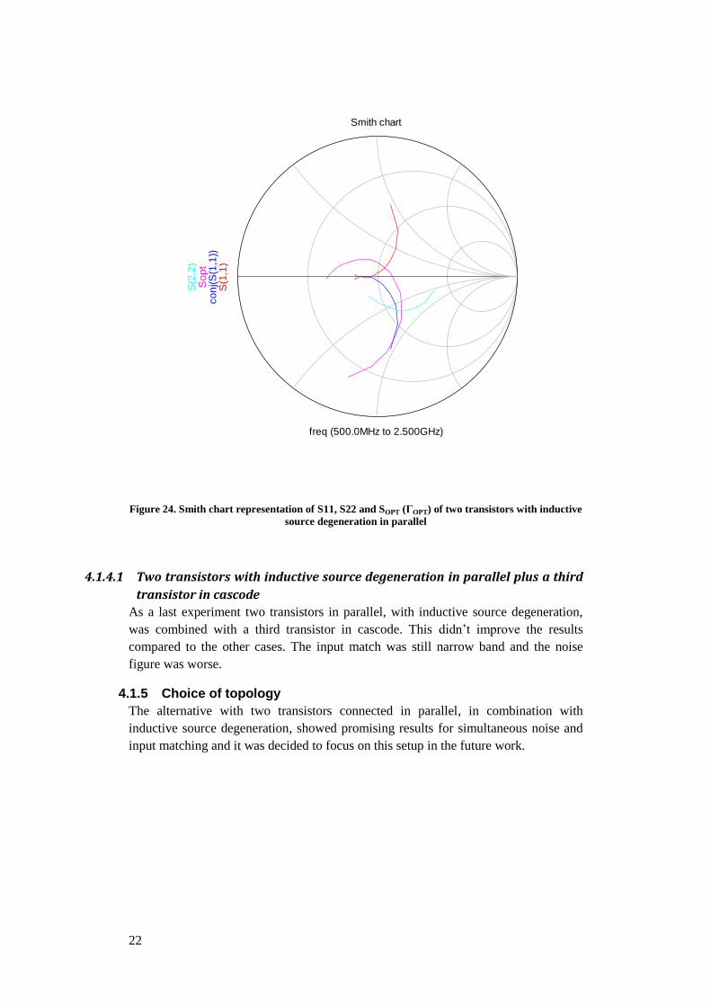
band, see Figure 23. In the smith chart in Figure 24 curves for S11* and SOPT (ΓOPT)
are close to each other and to 50 Ohm (the center of the chart).
21
Figure 22. S-parameters of two transistors with inductive source degeneration in parallel
Figure 23. NF of two transistors with inductive source degeneration in parallel
0.6 0.8 1.0 1.2 1.4 1.6 1.8 2.0 2.2 2.40.4 2.6
-50
-40
-30
-20
-10
0
10
20
-60
30
freq, GHz
dB
(S(1
,1))
dB
(S(2
,2))
dB
(S(2
,1))
dB
(S(1
,2))
S-parameters
0.6 0.8 1.0 1.2 1.4 1.6 1.8 2.0 2.2 2.40.4 2.6
0.5
1.0
1.5
2.0
0.0
2.5
freq, GHz
nf(
2)
NF
min
NF
22
Figure 24. Smith chart representation of S11, S22 and SOPT (ΓOPT) of two transistors with inductive
source degeneration in parallel
4.1.4.1 Two transistors with inductive source degeneration in parallel plus a third
transistor in cascode
As a last experiment two transistors in parallel, with inductive source degeneration,
was combined with a third transistor in cascode. This didn’t improve the results
compared to the other cases. The input match was still narrow band and the noise
figure was worse.
4.1.5 Choice of topology
The alternative with two transistors connected in parallel, in combination with
inductive source degeneration, showed promising results for simultaneous noise and
input matching and it was decided to focus on this setup in the future work.
freq (500.0MHz to 2.500GHz)
S(1
,1)
co
nj(S
(1,1
))S
op
tS
(2,2
)
Smith chart
23
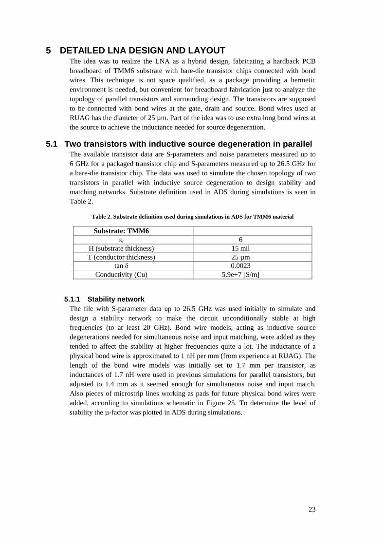
5 DETAILED LNA DESIGN AND LAYOUT The idea was to realize the LNA as a hybrid design, fabricating a hardback PCB
breadboard of TMM6 substrate with bare-die transistor chips connected with bond
wires. This technique is not space qualified, as a package providing a hermetic
environment is needed, but convenient for breadboard fabrication just to analyze the
topology of parallel transistors and surrounding design. The transistors are supposed
to be connected with bond wires at the gate, drain and source. Bond wires used at
RUAG has the diameter of 25 µm. Part of the idea was to use extra long bond wires at
the source to achieve the inductance needed for source degeneration.
5.1 Two transistors with inductive source degeneration in parallel The available transistor data are S-parameters and noise parameters measured up to
6 GHz for a packaged transistor chip and S-parameters measured up to 26.5 GHz for
a bare-die transistor chip. The data was used to simulate the chosen topology of two
transistors in parallel with inductive source degeneration to design stability and
matching networks. Substrate definition used in ADS during simulations is seen in
Table 2.
Table 2. Substrate definition used during simulations in ADS for TMM6 material
Substrate: TMM6
εr 6
H (substrate thickness) 15 mil
T (conductor thickness) 25 µm
tan δ 0.0023
Conductivity (Cu) 5.9e+7 [S/m]
5.1.1 Stability network
The file with S-parameter data up to 26.5 GHz was used initially to simulate and
design a stability network to make the circuit unconditionally stable at high
frequencies (to at least 20 GHz). Bond wire models, acting as inductive source
degenerations needed for simultaneous noise and input matching, were added as they
tended to affect the stability at higher frequencies quite a lot. The inductance of a
physical bond wire is approximated to 1 nH per mm (from experience at RUAG). The
length of the bond wire models was initially set to 1.7 mm per transistor, as
inductances of 1.7 nH were used in previous simulations for parallel transistors, but
adjusted to 1.4 mm as it seemed enough for simultaneous noise and input match.
Also pieces of microstrip lines working as pads for future physical bond wires were
added, according to simulations schematic in Figure 25. To determine the level of
stability the µ-factor was plotted in ADS during simulations.
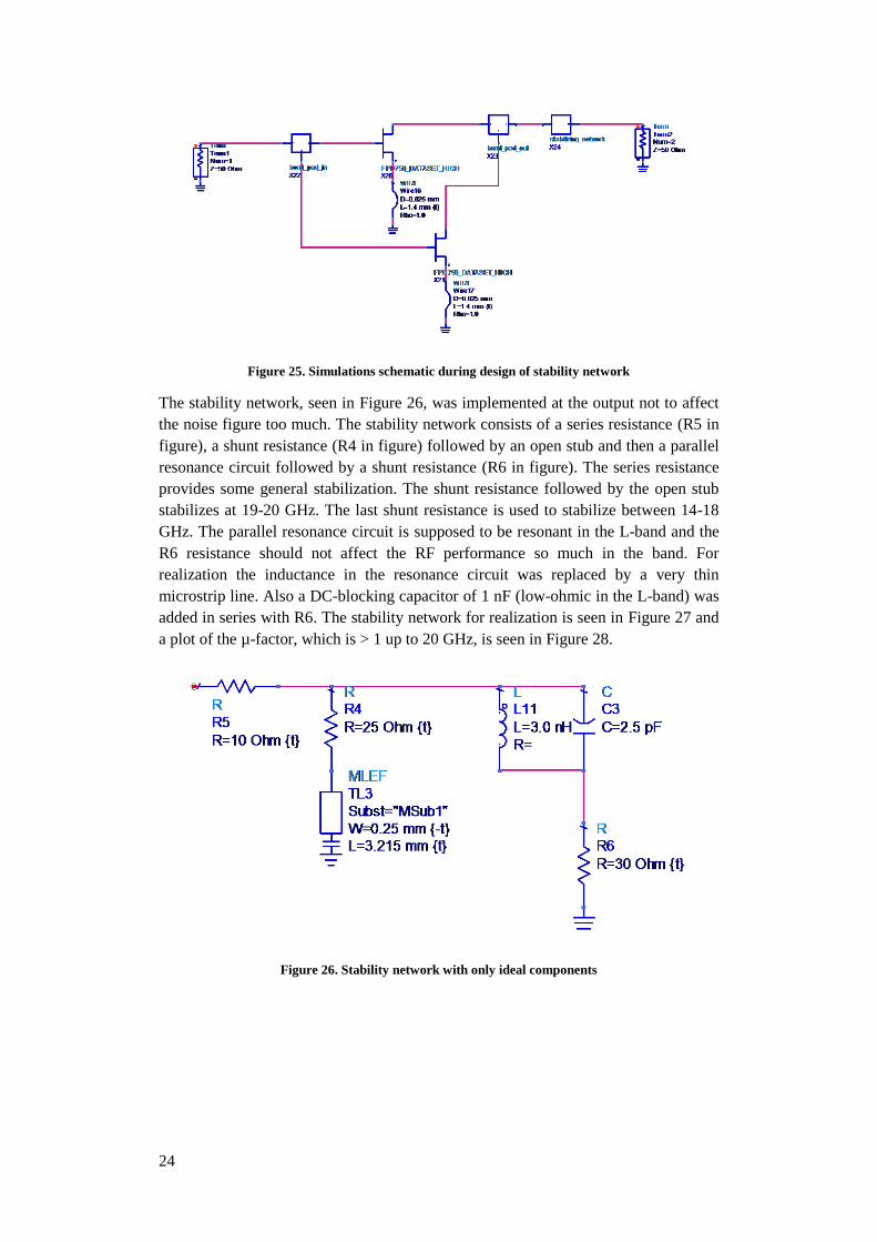
24
Figure 25. Simulations schematic during design of stability network
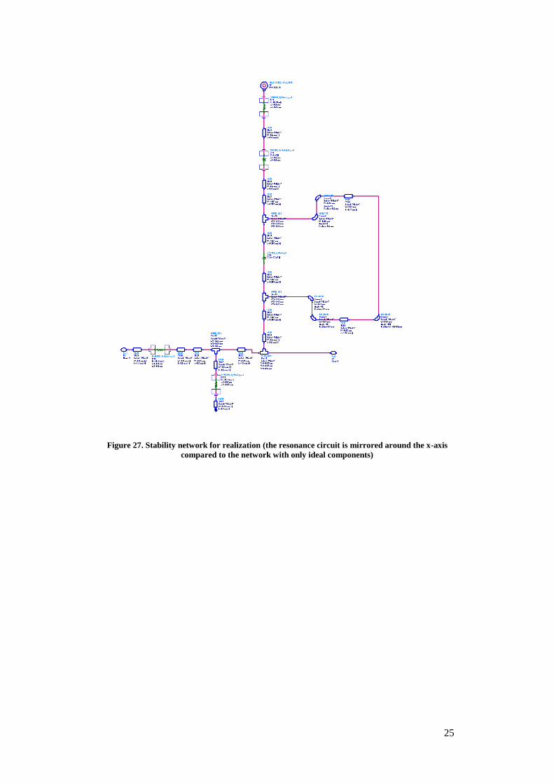
The stability network, seen in Figure 26, was implemented at the output not to affect
the noise figure too much. The stability network consists of a series resistance (R5 in
figure), a shunt resistance (R4 in figure) followed by an open stub and then a parallel
resonance circuit followed by a shunt resistance (R6 in figure). The series resistance
provides some general stabilization. The shunt resistance followed by the open stub
stabilizes at 19-20 GHz. The last shunt resistance is used to stabilize between 14-18
GHz. The parallel resonance circuit is supposed to be resonant in the L-band and the
R6 resistance should not affect the RF performance so much in the band. For
realization the inductance in the resonance circuit was replaced by a very thin
microstrip line. Also a DC-blocking capacitor of 1 nF (low-ohmic in the L-band) was
added in series with R6. The stability network for realization is seen in Figure 27 and
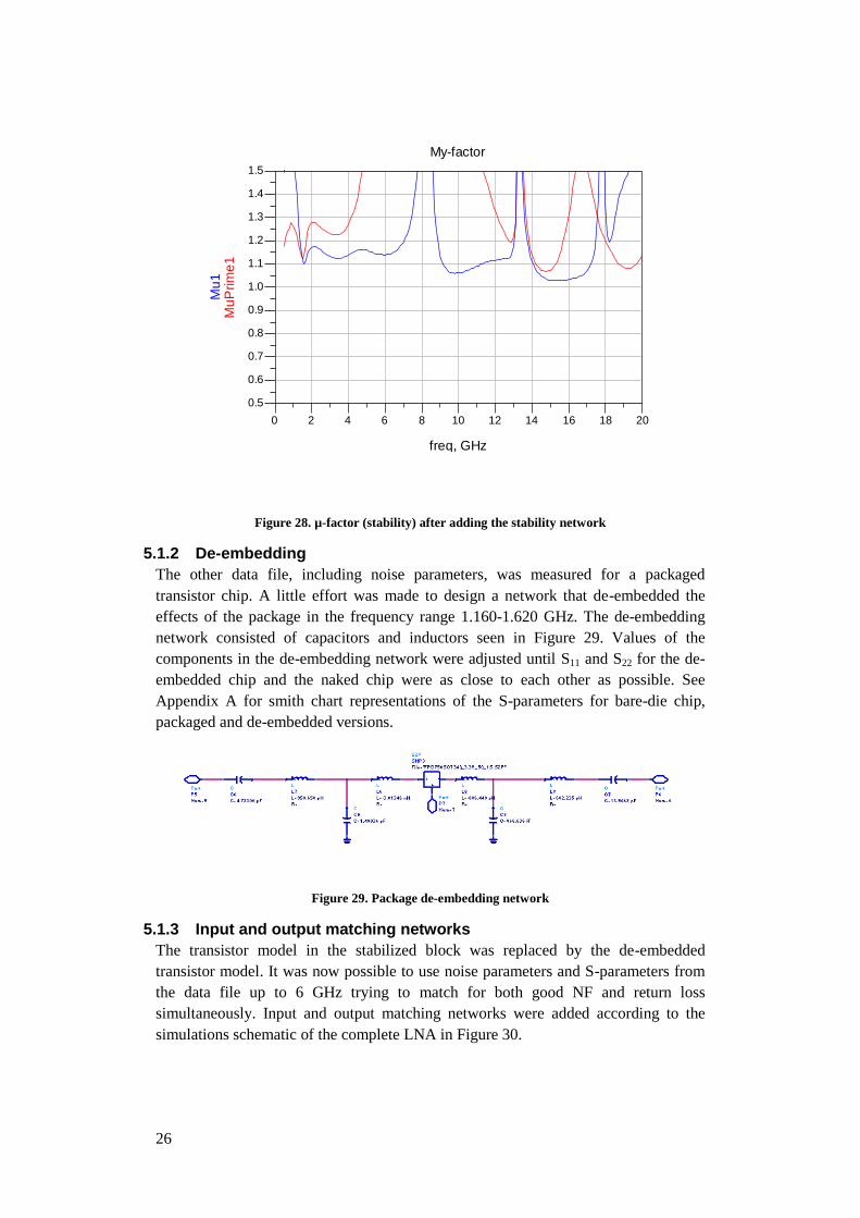
a plot of the µ-factor, which is > 1 up to 20 GHz, is seen in Figure 28.
Figure 26. Stability network with only ideal components
25
Figure 27. Stability network for realization (the resonance circuit is mirrored around the x-axis
compared to the network with only ideal components)
26
Figure 28. µ-factor (stability) after adding the stability network
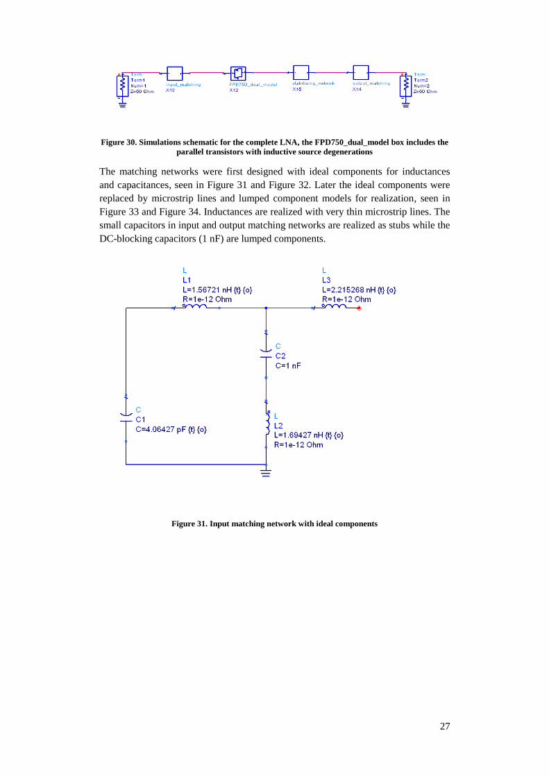
5.1.2 De-embedding
The other data file, including noise parameters, was measured for a packaged
transistor chip. A little effort was made to design a network that de-embedded the
effects of the package in the frequency range 1.160-1.620 GHz. The de-embedding
network consisted of capacitors and inductors seen in Figure 29. Values of the
components in the de-embedding network were adjusted until S11 and S22 for the de-
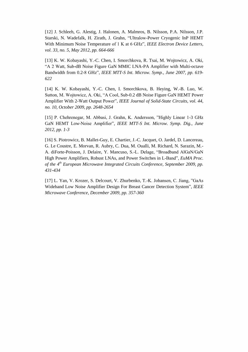
embedded chip and the naked chip were as close to each other as possible. See
Appendix A for smith chart representations of the S-parameters for bare-die chip,
packaged and de-embedded versions.
Figure 29. Package de-embedding network
5.1.3 Input and output matching networks
The transistor model in the stabilized block was replaced by the de-embedded
transistor model. It was now possible to use noise parameters and S-parameters from
the data file up to 6 GHz trying to match for both good NF and return loss
simultaneously. Input and output matching networks were added according to the
simulations schematic of the complete LNA in Figure 30.
2 4 6 8 10 12 14 16 180 20
0.6
0.7
0.8
0.9
1.0
1.1
1.2
1.3
1.4
0.5
1.5
freq, GHz
Mu
Prim
e1
Mu
1
My-factor
27
Figure 30. Simulations schematic for the complete LNA, the FPD750_dual_model box includes the
parallel transistors with inductive source degenerations
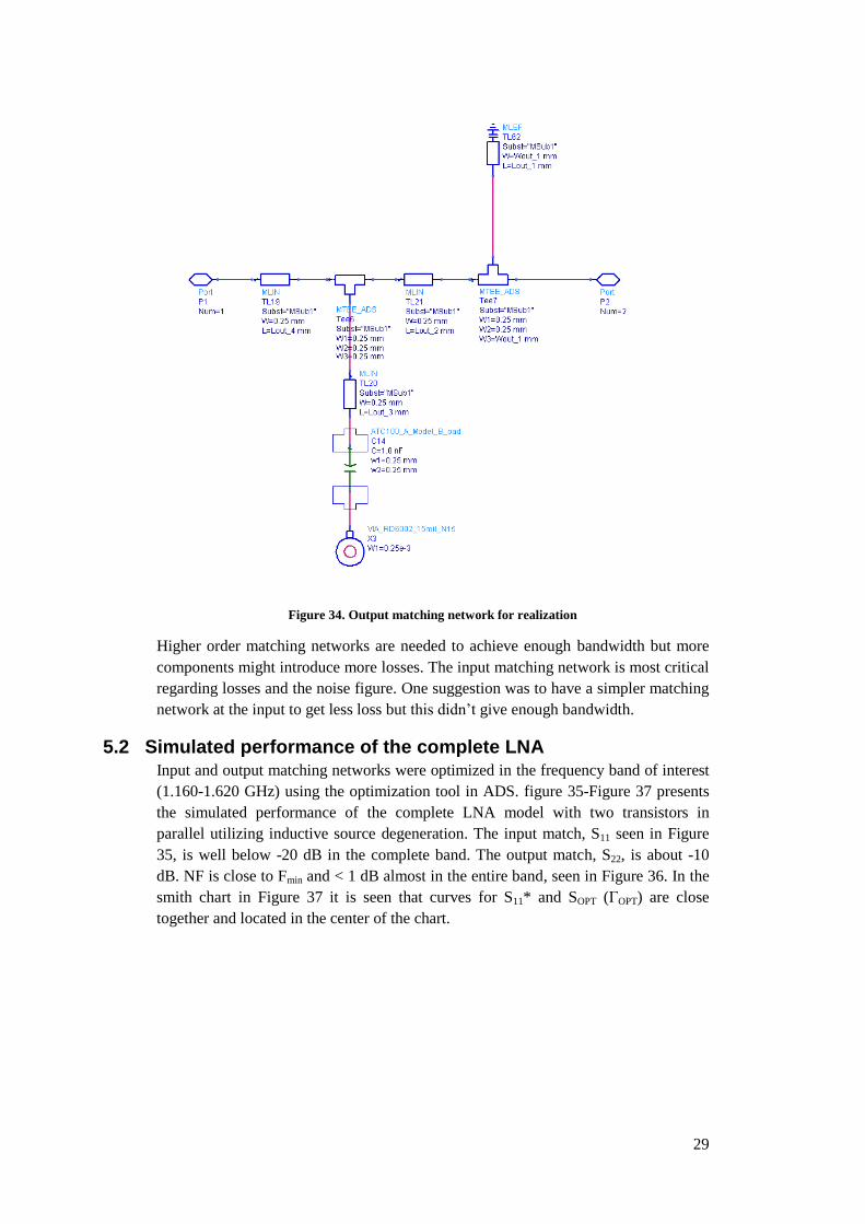
The matching networks were first designed with ideal components for inductances
and capacitances, seen in Figure 31 and Figure 32. Later the ideal components were
replaced by microstrip lines and lumped component models for realization, seen in
Figure 33 and Figure 34. Inductances are realized with very thin microstrip lines. The
small capacitors in input and output matching networks are realized as stubs while the
DC-blocking capacitors (1 nF) are lumped components.
Figure 31. Input matching network with ideal components
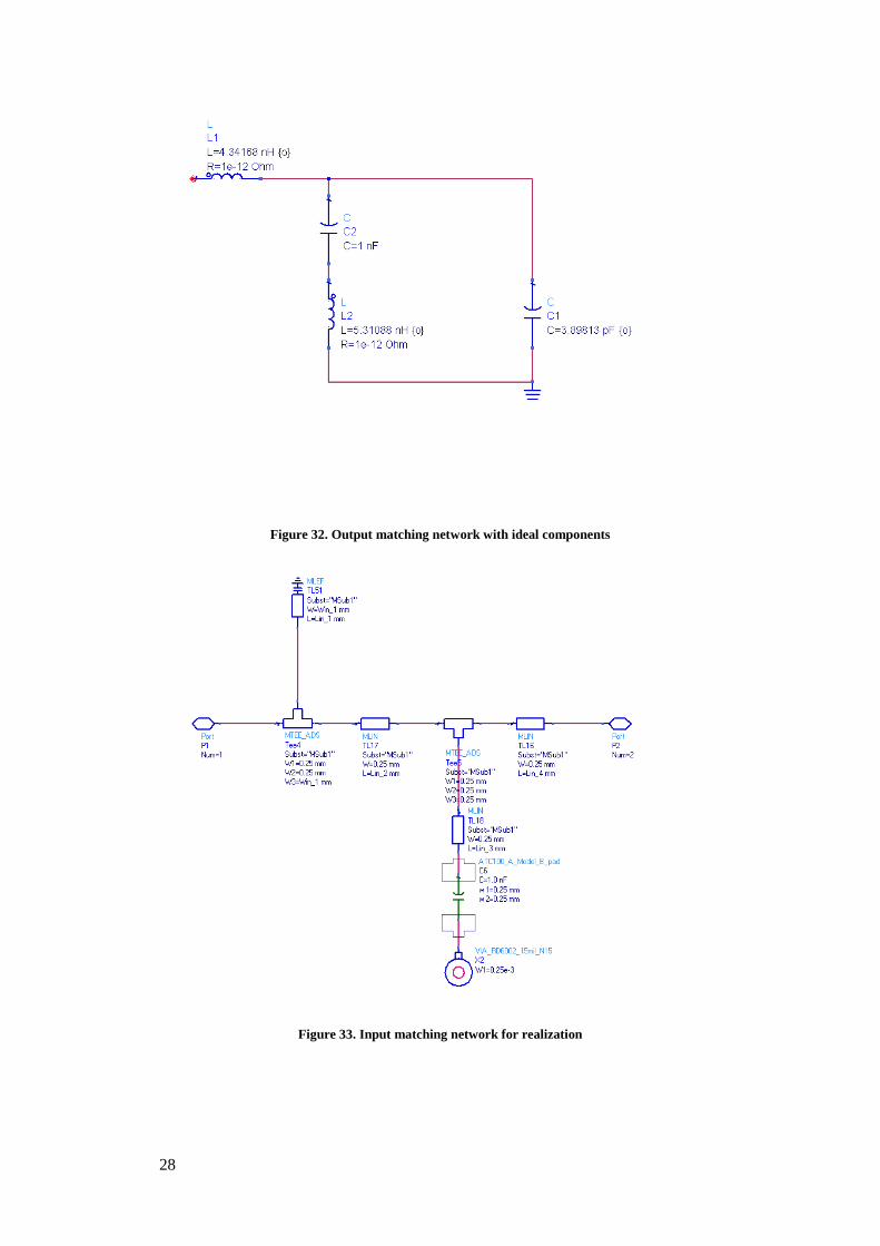
28
Figure 32. Output matching network with ideal components
Figure 33. Input matching network for realization
29
Figure 34. Output matching network for realization
Higher order matching networks are needed to achieve enough bandwidth but more
components might introduce more losses. The input matching network is most critical
regarding losses and the noise figure. One suggestion was to have a simpler matching
network at the input to get less loss but this didn’t give enough bandwidth.
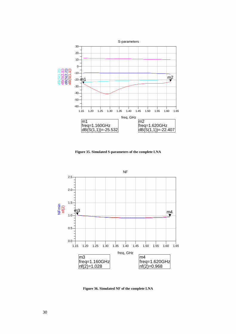
5.2 Simulated performance of the complete LNA
Input and output matching networks were optimized in the frequency band of interest
(1.160-1.620 GHz) using the optimization tool in ADS. figure 35-Figure 37 presents
the simulated performance of the complete LNA model with two transistors in
parallel utilizing inductive source degeneration. The input match, S11 seen in Figure
35, is well below -20 dB in the complete band. The output match, S22, is about -10
dB. NF is close to Fmin and < 1 dB almost in the entire band, seen in Figure 36. In the
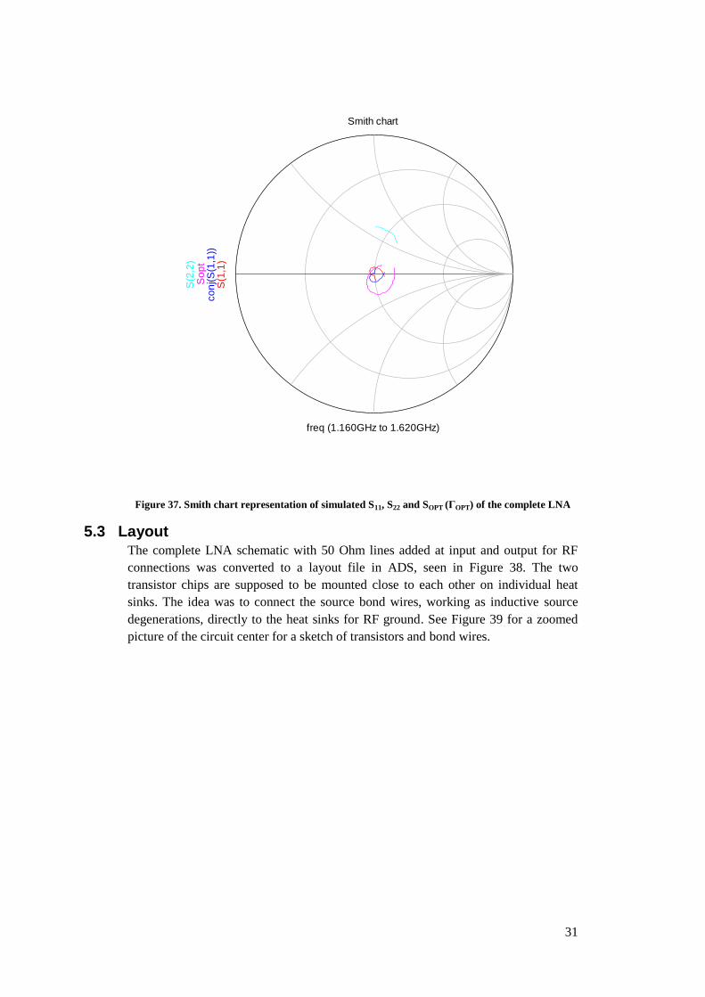
smith chart in Figure 37 it is seen that curves for S11* and SOPT (ΓOPT) are close
together and located in the center of the chart.
30
Figure 35. Simulated S-parameters of the complete LNA
Figure 36. Simulated NF of the complete LNA
1.20 1.25 1.30 1.35 1.40 1.45 1.50 1.55 1.601.15 1.65
-50
-40
-30
-20
-10
0
10
20
-60
30
freq, GHz
dB
(S(1
,1))
Readout
m1
Readout
m2
dB
(S(2
,2))
dB
(S(2
,1))
dB
(S(1
,2))
S-parameters
m1freq=dB(S(1,1))=-25.532
1.160GHzm2freq=dB(S(1,1))=-22.407
1.620GHz
1.20 1.25 1.30 1.35 1.40 1.45 1.50 1.55 1.601.15 1.65
0.5
1.0
1.5
2.0
0.0
2.5
freq, GHz
nf(
2)
Readout
m3
Readout
m4NF
min
NF
m3freq=nf(2)=1.028
1.160GHzm4freq=nf(2)=0.968
1.620GHz
31
Figure 37. Smith chart representation of simulated S11, S22 and SOPT (ΓOPT) of the complete LNA
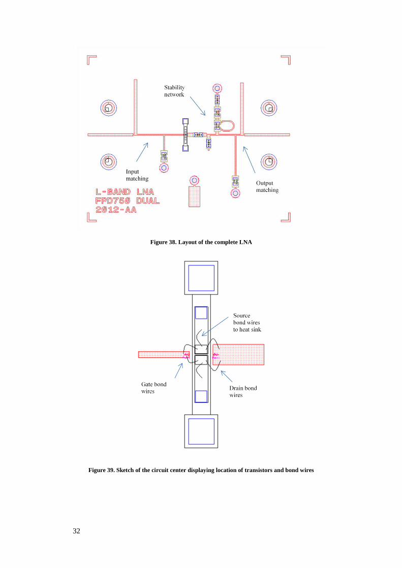
5.3 Layout The complete LNA schematic with 50 Ohm lines added at input and output for RF
connections was converted to a layout file in ADS, seen in Figure 38. The two
transistor chips are supposed to be mounted close to each other on individual heat
sinks. The idea was to connect the source bond wires, working as inductive source
degenerations, directly to the heat sinks for RF ground. See Figure 39 for a zoomed
picture of the circuit center for a sketch of transistors and bond wires.
freq (1.160GHz to 1.620GHz)
S(1
,1)
co
nj(S
(1,1
))S
op
tS
(2,2
)
Smith chart
32
Figure 38. Layout of the complete LNA
Figure 39. Sketch of the circuit center displaying location of transistors and bond wires
33
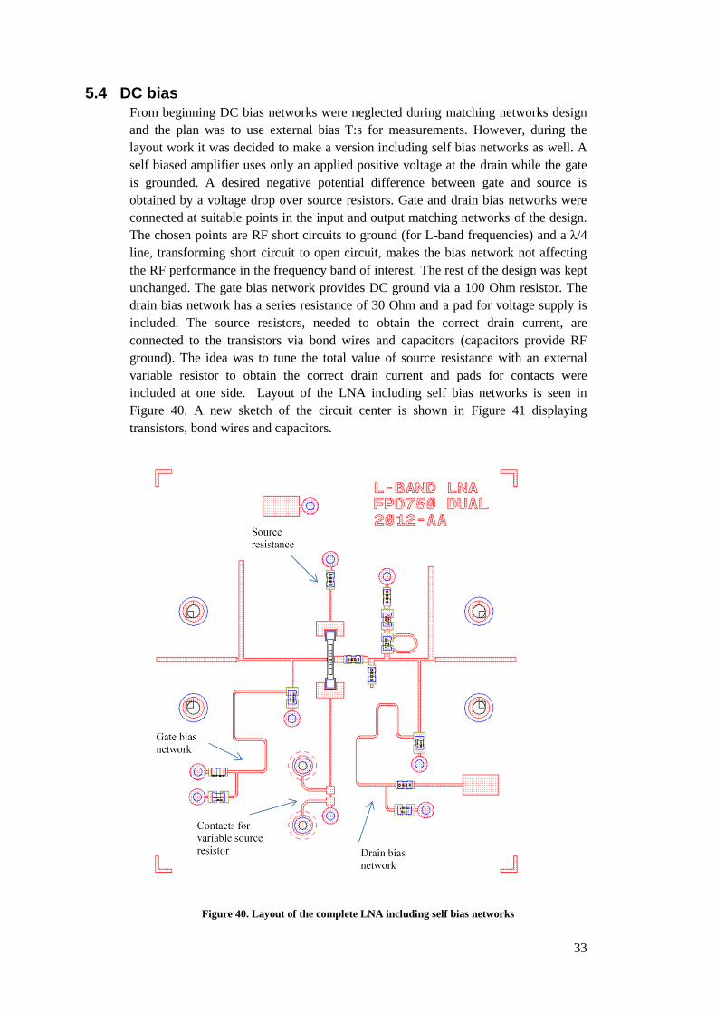
5.4 DC bias
From beginning DC bias networks were neglected during matching networks design
and the plan was to use external bias T:s for measurements. However, during the
layout work it was decided to make a version including self bias networks as well. A
self biased amplifier uses only an applied positive voltage at the drain while the gate
is grounded. A desired negative potential difference between gate and source is
obtained by a voltage drop over source resistors. Gate and drain bias networks were
connected at suitable points in the input and output matching networks of the design.
The chosen points are RF short circuits to ground (for L-band frequencies) and a λ/4
line, transforming short circuit to open circuit, makes the bias network not affecting
the RF performance in the frequency band of interest. The rest of the design was kept
unchanged. The gate bias network provides DC ground via a 100 Ohm resistor. The
drain bias network has a series resistance of 30 Ohm and a pad for voltage supply is
included. The source resistors, needed to obtain the correct drain current, are
connected to the transistors via bond wires and capacitors (capacitors provide RF
ground). The idea was to tune the total value of source resistance with an external
variable resistor to obtain the correct drain current and pads for contacts were
included at one side. Layout of the LNA including self bias networks is seen in
Figure 40. A new sketch of the circuit center is shown in Figure 41 displaying
transistors, bond wires and capacitors.
Figure 40. Layout of the complete LNA including self bias networks
34
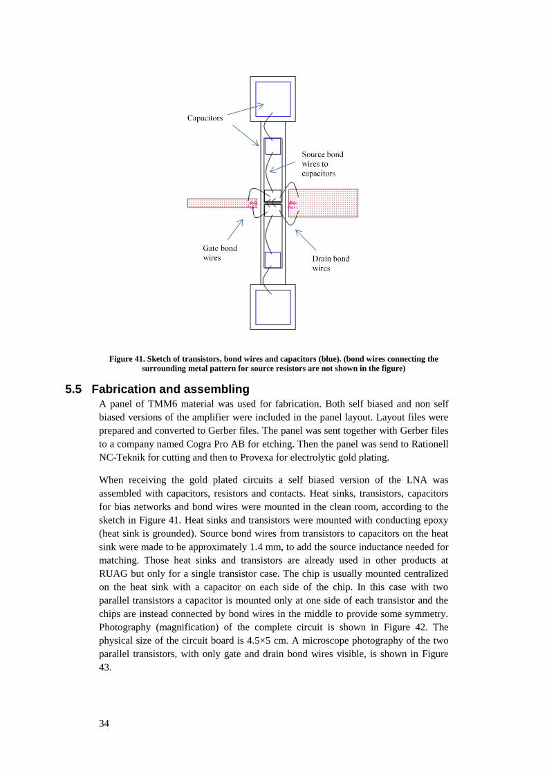
Figure 41. Sketch of transistors, bond wires and capacitors (blue). (bond wires connecting the
surrounding metal pattern for source resistors are not shown in the figure)
5.5 Fabrication and assembling A panel of TMM6 material was used for fabrication. Both self biased and non self
biased versions of the amplifier were included in the panel layout. Layout files were
prepared and converted to Gerber files. The panel was sent together with Gerber files
to a company named Cogra Pro AB for etching. Then the panel was send to Rationell
NC-Teknik for cutting and then to Provexa for electrolytic gold plating.
When receiving the gold plated circuits a self biased version of the LNA was
assembled with capacitors, resistors and contacts. Heat sinks, transistors, capacitors
for bias networks and bond wires were mounted in the clean room, according to the
sketch in Figure 41. Heat sinks and transistors were mounted with conducting epoxy
(heat sink is grounded). Source bond wires from transistors to capacitors on the heat
sink were made to be approximately 1.4 mm, to add the source inductance needed for
matching. Those heat sinks and transistors are already used in other products at
RUAG but only for a single transistor case. The chip is usually mounted centralized
on the heat sink with a capacitor on each side of the chip. In this case with two
parallel transistors a capacitor is mounted only at one side of each transistor and the
chips are instead connected by bond wires in the middle to provide some symmetry.
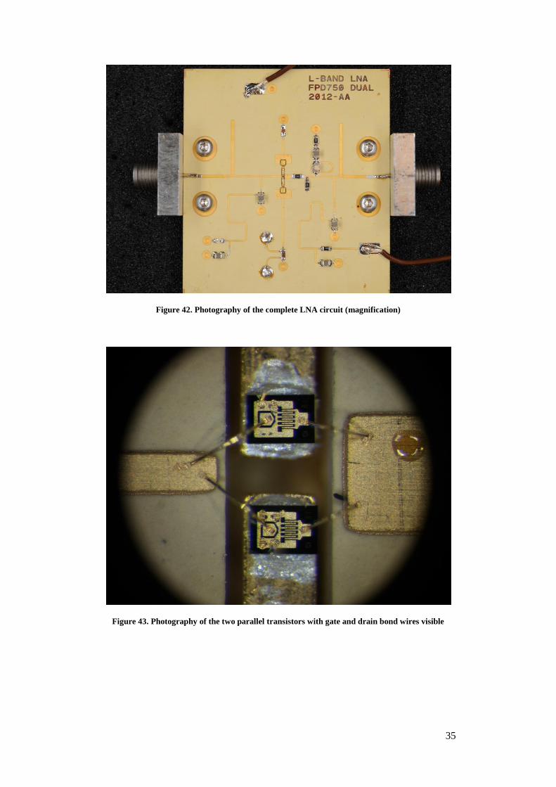
Photography (magnification) of the complete circuit is shown in Figure 42. The
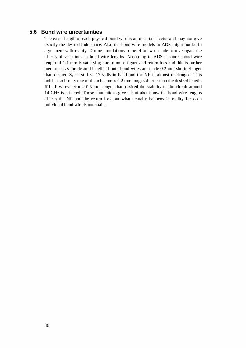
physical size of the circuit board is 4.5×5 cm. A microscope photography of the two
parallel transistors, with only gate and drain bond wires visible, is shown in Figure
43.
35
Figure 42. Photography of the complete LNA circuit (magnification)
Figure 43. Photography of the two parallel transistors with gate and drain bond wires visible
36
5.6 Bond wire uncertainties
The exact length of each physical bond wire is an uncertain factor and may not give
exactly the desired inductance. Also the bond wire models in ADS might not be in
agreement with reality. During simulations some effort was made to investigate the
effects of variations in bond wire lengths. According to ADS a source bond wire
length of 1.4 mm is satisfying due to noise figure and return loss and this is further
mentioned as the desired length. If both bond wires are made 0.2 mm shorter/longer
than desired S11 is still < -17.5 dB in band and the NF is almost unchanged. This
holds also if only one of them becomes 0.2 mm longer/shorter than the desired length.
If both wires become 0.3 mm longer than desired the stability of the circuit around
14 GHz is affected. Those simulations give a hint about how the bond wire lengths
affects the NF and the return loss but what actually happens in reality for each
individual bond wire is uncertain.
37
6 MEASUREMENTS AND RESULTS
6.1 Bias tuning During simulations transistor data for DC bias Vd=3.3 V and Id=50 mA per transistor
was used. As two transistors are put in parallel the total current is supposed to be
Id=100 mA when the LNA is in use (and during measurements). A total series
resistance of 40 Ohm at the drain gives a voltage drop of 4 V for Id=100 mA and the
applied voltage should be 3.3+4=7.3 V. The strategy was to tune the total source
resistance using an external variable resistor to obtain Id=100 mA. This voltage drop
over the source resistors should result in a negative potential difference between gate
and source as the gate is grounded. According to transistor data Vp is approximately
-0.6 V.
When trying to tune the source resistance, to obtain the correct bias, stability
problems were discovered. The LNA was unstable at approximately 17 GHz and it
was not possible to obtain Id=100 mA. The oscillation problem resulted in a negative
potential at the gate even though the gate is supposed to have zero potential. Because
of uncertainties with the combination of long source bond wires and capacitors,
connecting transistors and source resistors, the circuit was modified a bit. Sources of
the transistors were grounded without resistors and an external bias T was used
instead to apply a negative voltage at the gate.
Pieces of a field absorbing material, Eccosorb, was placed on different parts of the
circuit to see if there were any critical areas regarding the stability problem. No
obvious effects were seen and the hypothesis was that reasons for the stability
problem were coupled to the area close to the transistors. To exclude any problems
with broken transistors and breakdown phenomena DC parameters were measured
and compared with tables. The transistors seemed intact anyhow.
After going back doing some simulations in ADS it was decided to remove the
source-to-source bond wires connecting the two transistors as they tended to affect
the stability. According to simulations also the length of gate and drain bond wires
affected the stability quite a lot. Even though the source-to-source bond wires were
removed there were still some stability problems at 10 and 18-19 GHz when trying to
biasing the amplifier. It was only possible to reach Id=10 mA before oscillations
appeared. As an experiment one of the transistors was disabled by means of removing
gate, drain and source bond wires for this chip. It was now possible to bias the circuit
with Vd=3.3 V and Id=25 mA for this single transistor case. Anyhow the situation was
not satisfying and the length of the source bond wires (the inductive source
degenerations) was up for discussion as a critical factor due to stability. It was seen
already during simulations that long source bond wires, needed for simultaneous
noise and input match, can become a problem regarding high frequency stability. This
was considered during design of the stability network but perhaps it was not working
sufficiently enough in reality. The remaining source bond wire was removed and a
new, shorter one was connected to the source and attached directly to the heat sink
providing RF and DC ground, like in the original design. The capacitors were not
necessary anyway as the circuit was no longer self biased and an external bias T was
used at the gate. With a shorter source bond wire improved stability was predicted,
but also degraded NF and input match.
38
Finally the LNA was stable also at higher frequencies and possible to bias correctly
(Vd=3.3 V and Id=50 mA) and Vgs≈-0.73 V. If measurements from this single
transistor version of the LNA showed promising results the plan was to connect the
other transistor chip again, also with a shorter source bond wire directly to the heat
sink to maintain stability.
6.2 RF measurements
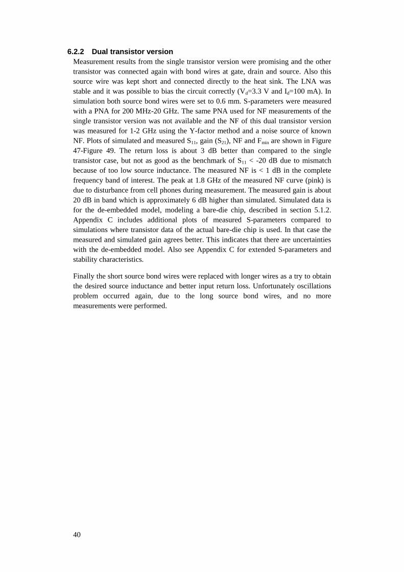
6.2.1 Single transistor version
S-parameters of the single transistor version of the LNA were measured with a power
network analyzer (PNA). Also NF was measured with the PNA (cold source
measurement). Noise is relevant to measure in band and so the NF was measured for
1-2 GHz, while S-parameters were measured for 100 MHz-20 GHz. During
measurements bias was applied through the PNA. Plots of simulated and measured
S11, gain (S21), NF and Fmin are shown in Figure 44-Figure 46. S-parameters are
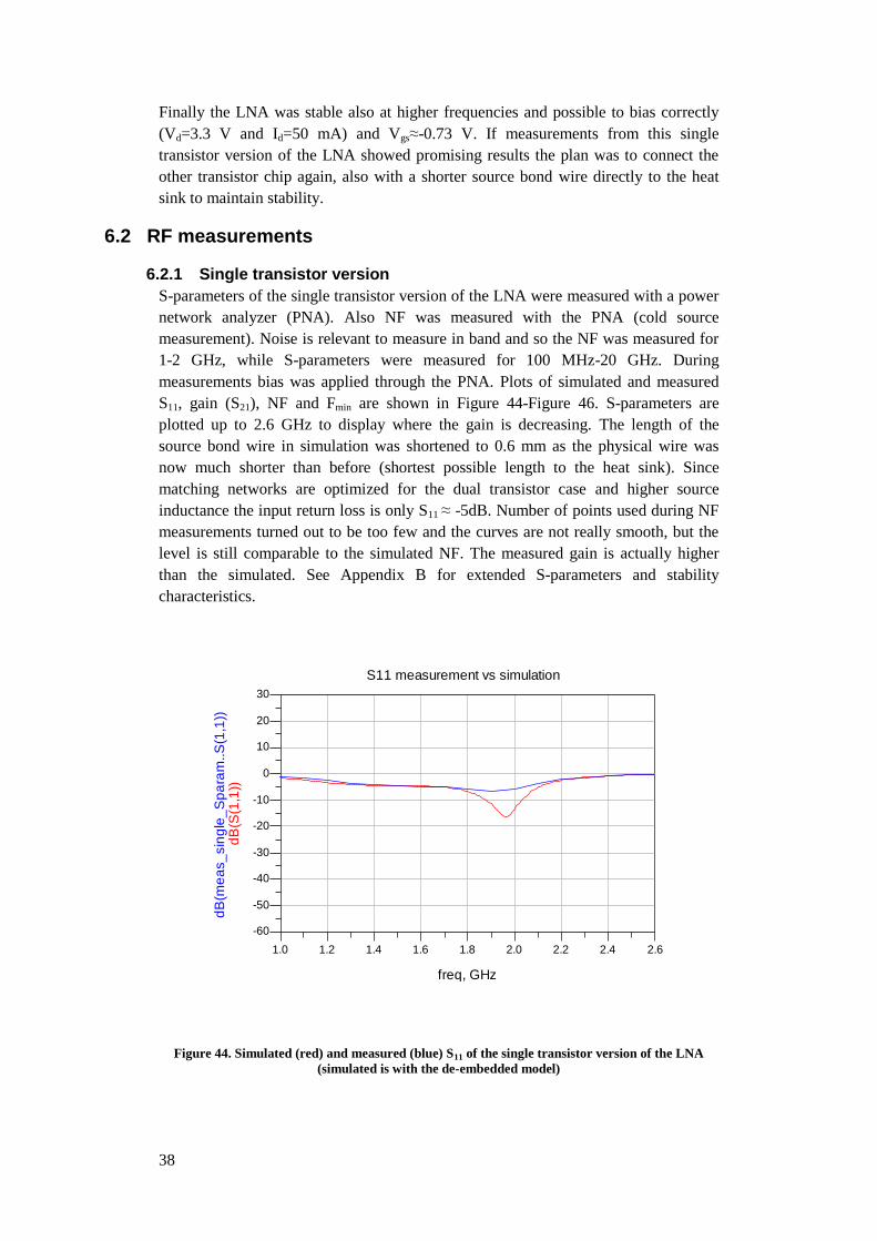
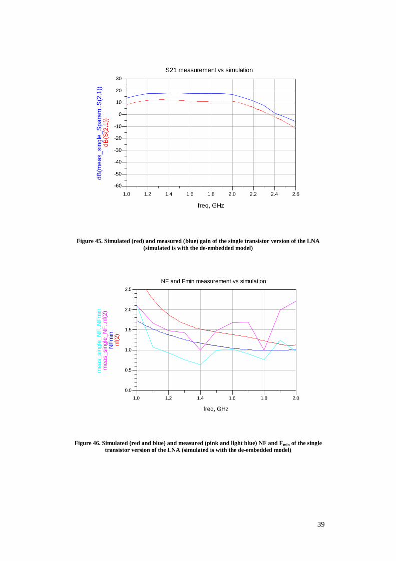
plotted up to 2.6 GHz to display where the gain is decreasing. The length of the
source bond wire in simulation was shortened to 0.6 mm as the physical wire was
now much shorter than before (shortest possible length to the heat sink). Since
matching networks are optimized for the dual transistor case and higher source
inductance the input return loss is only S11 ≈ -5dB. Number of points used during NF
measurements turned out to be too few and the curves are not really smooth, but the
level is still comparable to the simulated NF. The measured gain is actually higher
than the simulated. See Appendix B for extended S-parameters and stability
characteristics.
Figure 44. Simulated (red) and measured (blue) S11 of the single transistor version of the LNA
(simulated is with the de-embedded model)
1.2 1.4 1.6 1.8 2.0 2.2 2.41.0 2.6
-50
-40
-30
-20
-10
0
10
20
-60
30
freq, GHz
dB
(S(1
,1))
dB
(me
as_
sin
gle
_S
pa
ram
..S
(1,1
))
S11 measurement vs simulation
39
Figure 45. Simulated (red) and measured (blue) gain of the single transistor version of the LNA
(simulated is with the de-embedded model)
Figure 46. Simulated (red and blue) and measured (pink and light blue) NF and Fmin of the single
transistor version of the LNA (simulated is with the de-embedded model)
1.2 1.4 1.6 1.8 2.0 2.2 2.41.0 2.6
-50
-40
-30
-20
-10
0
10
20
-60
30
freq, GHz
dB
(S(2
,1))
dB
(me
as_
sin
gle
_S
pa
ram
..S
(2,1
))
S21 measurement vs simulation
1.2 1.4 1.6 1.81.0 2.0
0.5
1.0
1.5
2.0
0.0
2.5
freq, GHz
nf(
2)
NF
min
meas_sin
gle
_N
F..nf(
2)
meas_sin
gle
_N
F..N
Fm
in
NF and Fmin measurement vs simulation
40
6.2.2 Dual transistor version
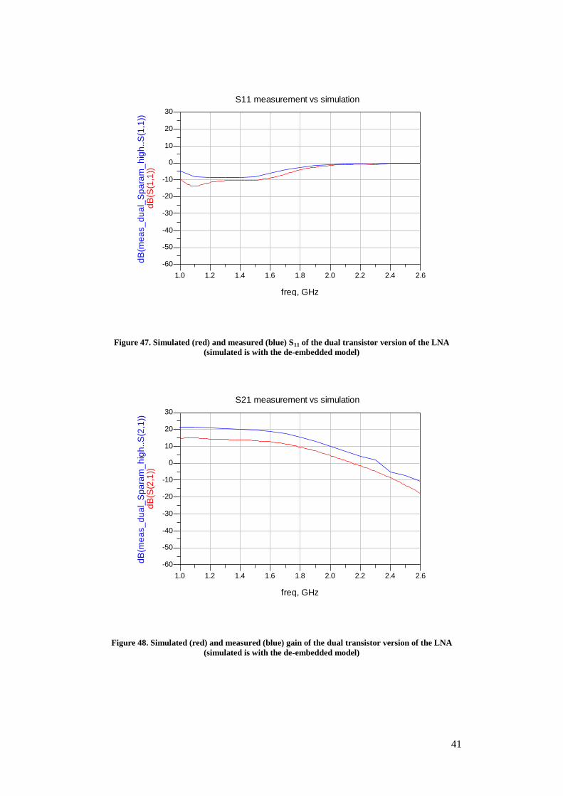
Measurement results from the single transistor version were promising and the other
transistor was connected again with bond wires at gate, drain and source. Also this
source wire was kept short and connected directly to the heat sink. The LNA was
stable and it was possible to bias the circuit correctly (Vd=3.3 V and Id=100 mA). In
simulation both source bond wires were set to 0.6 mm. S-parameters were measured
with a PNA for 200 MHz-20 GHz. The same PNA used for NF measurements of the
single transistor version was not available and the NF of this dual transistor version
was measured for 1-2 GHz using the Y-factor method and a noise source of known
NF. Plots of simulated and measured S11, gain (S21), NF and Fmin are shown in Figure
47-Figure 49. The return loss is about 3 dB better than compared to the single
transistor case, but not as good as the benchmark of S11 < -20 dB due to mismatch
because of too low source inductance. The measured NF is < 1 dB in the complete
frequency band of interest. The peak at 1.8 GHz of the measured NF curve (pink) is
due to disturbance from cell phones during measurement. The measured gain is about
20 dB in band which is approximately 6 dB higher than simulated. Simulated data is
for the de-embedded model, modeling a bare-die chip, described in section 5.1.2.
Appendix C includes additional plots of measured S-parameters compared to
simulations where transistor data of the actual bare-die chip is used. In that case the
measured and simulated gain agrees better. This indicates that there are uncertainties
with the de-embedded model. Also see Appendix C for extended S-parameters and
stability characteristics.
Finally the short source bond wires were replaced with longer wires as a try to obtain
the desired source inductance and better input return loss. Unfortunately oscillations
problem occurred again, due to the long source bond wires, and no more
measurements were performed.
41
Figure 47. Simulated (red) and measured (blue) S11 of the dual transistor version of the LNA
(simulated is with the de-embedded model)
Figure 48. Simulated (red) and measured (blue) gain of the dual transistor version of the LNA
(simulated is with the de-embedded model)
1.2 1.4 1.6 1.8 2.0 2.2 2.41.0 2.6
-50
-40
-30
-20
-10
0
10
20
-60
30
freq, GHz
dB
(S(1
,1))
dB
(me
as_
du
al_
Sp
ara
m_
hig
h..S
(1,1
))
S11 measurement vs simulation
1.2 1.4 1.6 1.8 2.0 2.2 2.41.0 2.6
-50
-40
-30
-20
-10
0
10
20
-60
30
freq, GHz
dB
(S(2
,1))
dB
(me
as_
du
al_
Sp
ara
m_
hig
h..S
(2,1
))
S21 measurement vs simulation
42
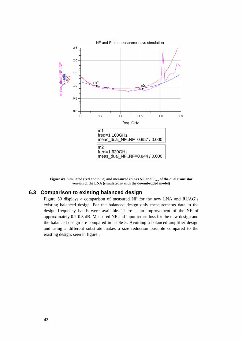
Figure 49. Simulated (red and blue) and measured (pink) NF and Fmin of the dual transistor
version of the LNA (simulated is with the de-embedded model)
6.3 Comparison to existing balanced design
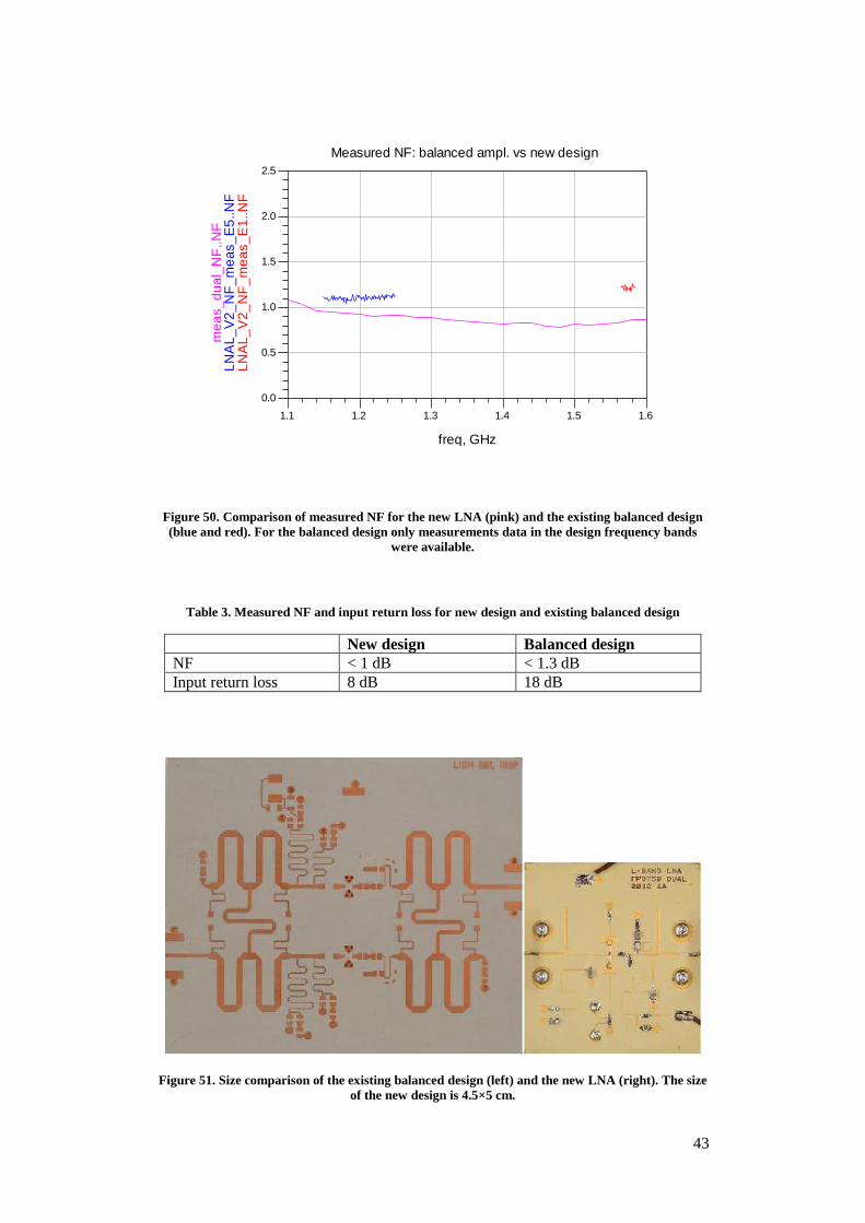
Figure 50 displays a comparison of measured NF for the new LNA and RUAG’s
existing balanced design. For the balanced design only measurements data in the
design frequency bands were available. There is an improvement of the NF of
approximately 0.2-0.3 dB. Measured NF and input return loss for the new design and
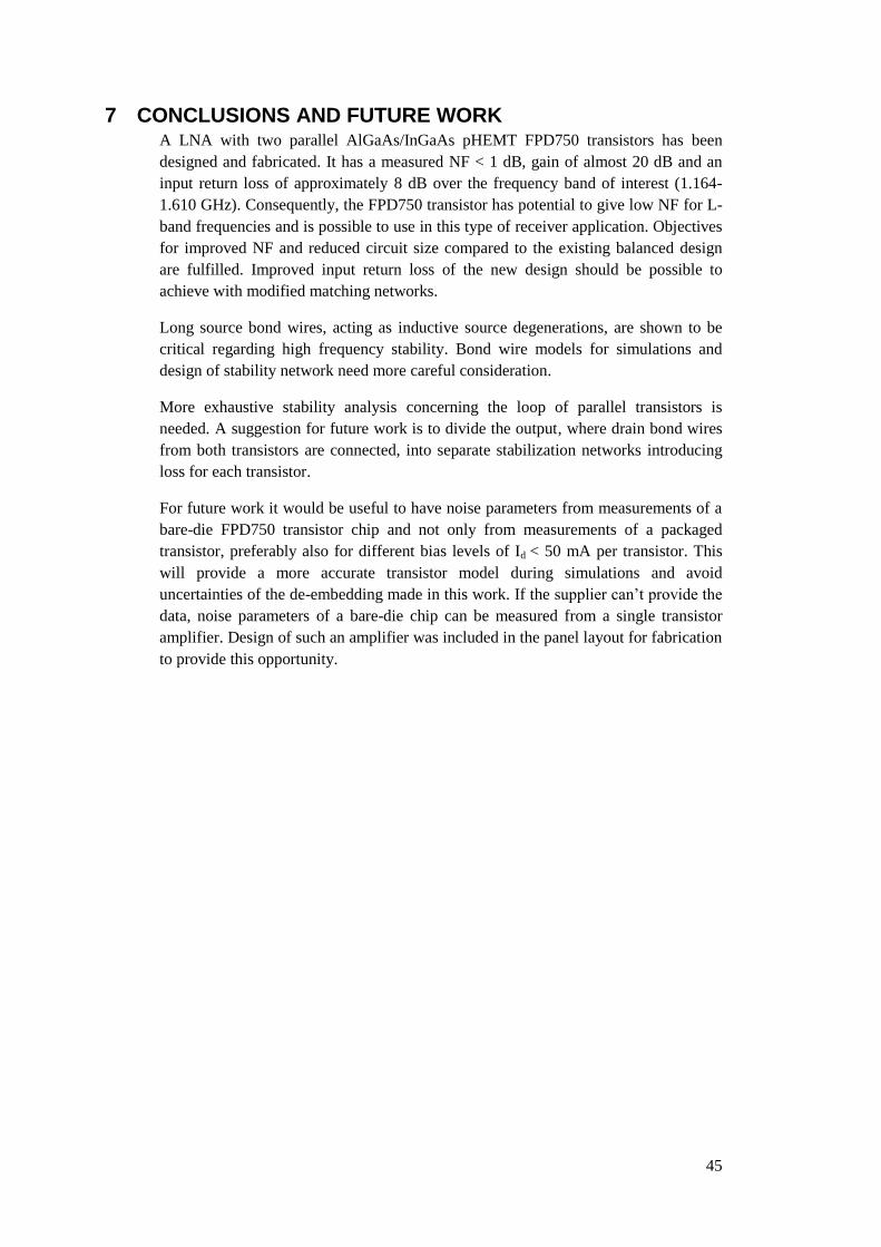
the balanced design are compared in Table 3. Avoiding a balanced amplifier design
and using a different substrate makes a size reduction possible compared to the
existing design, seen in figure .
1.2 1.4 1.6 1.81.0 2.0
0.5
1.0
1.5
2.0
0.0
2.5
freq, GHz
nf(
2)
NF
min
me
as_
du
al_
NF
..N
F
Readout
m1
Readout
m2
NF and Fmin measurement vs simulation
m1freq=meas_dual_NF..NF=0.957 / 0.000
1.160GHz
m2freq=meas_dual_NF..NF=0.844 / 0.000
1.620GHz
43
Figure 50. Comparison of measured NF for the new LNA (pink) and the existing balanced design
(blue and red). For the balanced design only measurements data in the design frequency bands
were available.
Table 3. Measured NF and input return loss for new design and existing balanced design
New design Balanced design
NF < 1 dB < 1.3 dB
Input return loss 8 dB 18 dB
Figure 51. Size comparison of the existing balanced design (left) and the new LNA (right). The size
of the new design is 4.5×5 cm.
1.2 1.3 1.4 1.51.1 1.6
0.5
1.0
1.5
2.0
0.0
2.5
freq, GHz
LN
AL
_V
2_
NF
_m
ea
s_
E1
..N
FL
NA
L_
V2
_N
F_
me
as_
E5
..N
Fm
ea
s_
du
al_
NF
..N
F
Measured NF: balanced ampl. vs new design

44
45
7 CONCLUSIONS AND FUTURE WORK A LNA with two parallel AlGaAs/InGaAs pHEMT FPD750 transistors has been
designed and fabricated. It has a measured NF < 1 dB, gain of almost 20 dB and an
input return loss of approximately 8 dB over the frequency band of interest (1.164-
1.610 GHz). Consequently, the FPD750 transistor has potential to give low NF for L-
band frequencies and is possible to use in this type of receiver application. Objectives
for improved NF and reduced circuit size compared to the existing balanced design
are fulfilled. Improved input return loss of the new design should be possible to
achieve with modified matching networks.
Long source bond wires, acting as inductive source degenerations, are shown to be
critical regarding high frequency stability. Bond wire models for simulations and
design of stability network need more careful consideration.
More exhaustive stability analysis concerning the loop of parallel transistors is
needed. A suggestion for future work is to divide the output, where drain bond wires
from both transistors are connected, into separate stabilization networks introducing
loss for each transistor.
For future work it would be useful to have noise parameters from measurements of a
bare-die FPD750 transistor chip and not only from measurements of a packaged
transistor, preferably also for different bias levels of Id < 50 mA per transistor. This
will provide a more accurate transistor model during simulations and avoid
uncertainties of the de-embedding made in this work. If the supplier can’t provide the
data, noise parameters of a bare-die chip can be measured from a single transistor
amplifier. Design of such an amplifier was included in the panel layout for fabrication
to provide this opportunity.

REFERENCES [1] P. Silvestrin, R. Bagge, M. Bonnedal, A. Carlström, J. Christensen, M. Hägg, T.
Lindgren, F. Zangerl, “Spaceborne GNSS Radio Occultation Instrumentation for
Operational Applications”, URL:
http://www.cosmic.ucar.edu/related_papers/2000_silvestrin_ion.pdf (2012-11-21)
[2] G. Gonzalez, “Microwave Transistor Amplifiers: Analysis and Design”, 2nd
ed.,
Prentice-Hall Inc. Upper Saddle River, 1997, ISBN 0-13-254335-4
[3] M. L. Edwards, J. H. Sinsky, “A New Criterion for Linear 2-Port Stability Using a
Single Geometrically Derived Parameter”, IEEE Transactions on microwave theory
and techniques, vol. 40, no. 12, December 1992, pp. 2303-2311
[4] T.-K. Nguyen, C.-H. Kim, G.-J. Ihm, M.-S. Yang, S.-G. Lee, “CMOS Low-Noise
Amplifier Design Optimization Techniques”, IEEE Transactions on microwave
theory and techniques, vol. 52, no. 5, May 2004, pp. 1433-1442
[5] S.-E. Shih, W. R. Deal, D. M. Yamauchi, W. E. Sutton, W.-B. Luo, Y. Chen, I. P.
Smorchkova, B. Heying, M. Wojtowicz, M. Siddiqui, “Design and Analysis of Ultra
Wideband GaN Dual-Gate HEMT Low-Noise Amplifiers”, IEEE Transactions on
microwave theory and techniques, vol. 57, no. 12, December 2009, pp. 3270-3277
[6] G. Girlando, G. Palmisano, “Noise Figure and Impedance Matching in RF
Cascode Amplifiers”, IEEE Transactions on circuits and systems – II: Analog and
digital signal processing, vol. 46, no. 11, November 1999, pp. 1388-1396
[7] S. E. Rosenbaum, L. M. Jelloian, L. E. Larson, U. K. Mishra, D. A. Pierson, M. S.
Thompson, T. Liu, A. S. Brown, “A 2-GHz Three-Stage AlInAs-GaInAs-InP HEMT
MMIC Low-Noise Amplifier”, IEEE Microwave and guided wave letters, vol. 3, no.
8, August 1993, pp. 265-267
[8] B. Boudjelida, A. Sobih, S. Arshad, A. Bouloukou, S. Boulay. J. Sly, M. Missous,
“Sub-0.5 dB NF broadband low-noise amplifier using a novel InGaAs/InAlAs/InP
pHEMT”, IEEE Advanced Semiconductor Devices and Microsystems, October 2008,
pp. 75-78
[9] P. S. Chen, D-H. Kim, J. Bergman, J. Hacker, B. Brar, ”Wideband Low-Noise-
Amplifier (LNA) with Lg = 50 nm InGaAs pHEMT and Wideband RF Chokes”, IEEE
MTT-S Int. Microw. Symp. Dig., June 2011
[10] A. Mellberg, N. Wadefalk, N. Rorsman, E. Choumas, J. Stenarson, I. Angelov,
P. Starski, E. Kollberg, J. Grahn, H. Zirath, ”InP HEMT-BASED, CRYOGENIC,
WIDEBAND LNAs FOR 4-8 GHz OPERATING AT VERY LOW DC-POWER”,
IEEE Indium Phosphide and Related Materials Conference, 2002, pp. 459-462
[11] A. Mellberg, N. Wadefalk, I. Angelov, E. Choumas, E. Kollberg, N. Rorsman, P.
Starski, J. Stenarson, H. Zirath, ”Cryogenic 2-4 GHz Ultra Low Noise Amplifier”,
IEEE MTT-S Digest, vol. 1, June 2004, pp. 161-163
[12] J. Schleeh, G. Alestig, J. Halonen, A. Malmros, B. Nilsson, P.A. Nilsson, J.P.
Starski, N. Wadefalk, H. Zirath, J. Grahn, “Ultralow-Power Cryogenic InP HEMT
With Minimum Noise Temperature of 1 K at 6 GHz”, IEEE Electron Device Letters,
vol. 33, no. 5, May 2012, pp. 664-666
[13] K. W. Kobayashi, Y.-C. Chen, I. Smorchkova, R. Tsai, M. Wojtowicz, A. Oki,
“A 2 Watt, Sub-dB Noise Figure GaN MMIC LNA-PA Amplifier with Multi-octave
Bandwidth from 0.2-8 GHz”, IEEE MTT-S Int. Microw. Symp., June 2007, pp. 619-
622
[14] K. W. Kobayashi, Y.-C. Chen, I. Smorchkova, B. Heying, W.-B. Luo, W.
Sutton, M. Wojtowicz, A. Oki, “A Cool, Sub-0.2 dB Noise Figure GaN HEMT Power
Amplifier With 2-Watt Output Power”, IEEE Journal of Solid-State Circuits, vol. 44,
no. 10, October 2009, pp. 2648-2654
[15] P. Chehrenegar, M. Abbasi, J. Grahn, K. Andersson, ”Highly Linear 1-3 GHz
GaN HEMT Low-Noise Amplifier”, IEEE MTT-S Int. Microw. Symp. Dig., June
2012, pp. 1-3
[16] S. Piotrowicz, B. Mallet-Guy, E. Chartier, J.-C. Jacquet, O. Jardel, D. Lancereau,
G. Le Coustre, E. Morvan, R. Aubry, C. Dua, M. Oualli, M. Richard, N. Sarazin, M.-
A. diForte-Poisson, J. Delaire, Y. Mancuso, S.-L. Delage, “Broadband AlGaN/GaN
High Power Amplifiers, Robust LNAs, and Power Switches in L-Band”, EuMA Proc.
of the 4th European Microwave Integrated Circuits Conference, September 2009, pp.
431-434
[17] L. Yan, V. Krozer, S. Delcourt, V. Zhurbenko, T.-K. Johansen, C. Jiang, ”GaAs
Wideband Low Noise Amplifier Design For Breast Cancer Detection System”, IEEE
Microwave Conference, December 2009, pp. 357-360


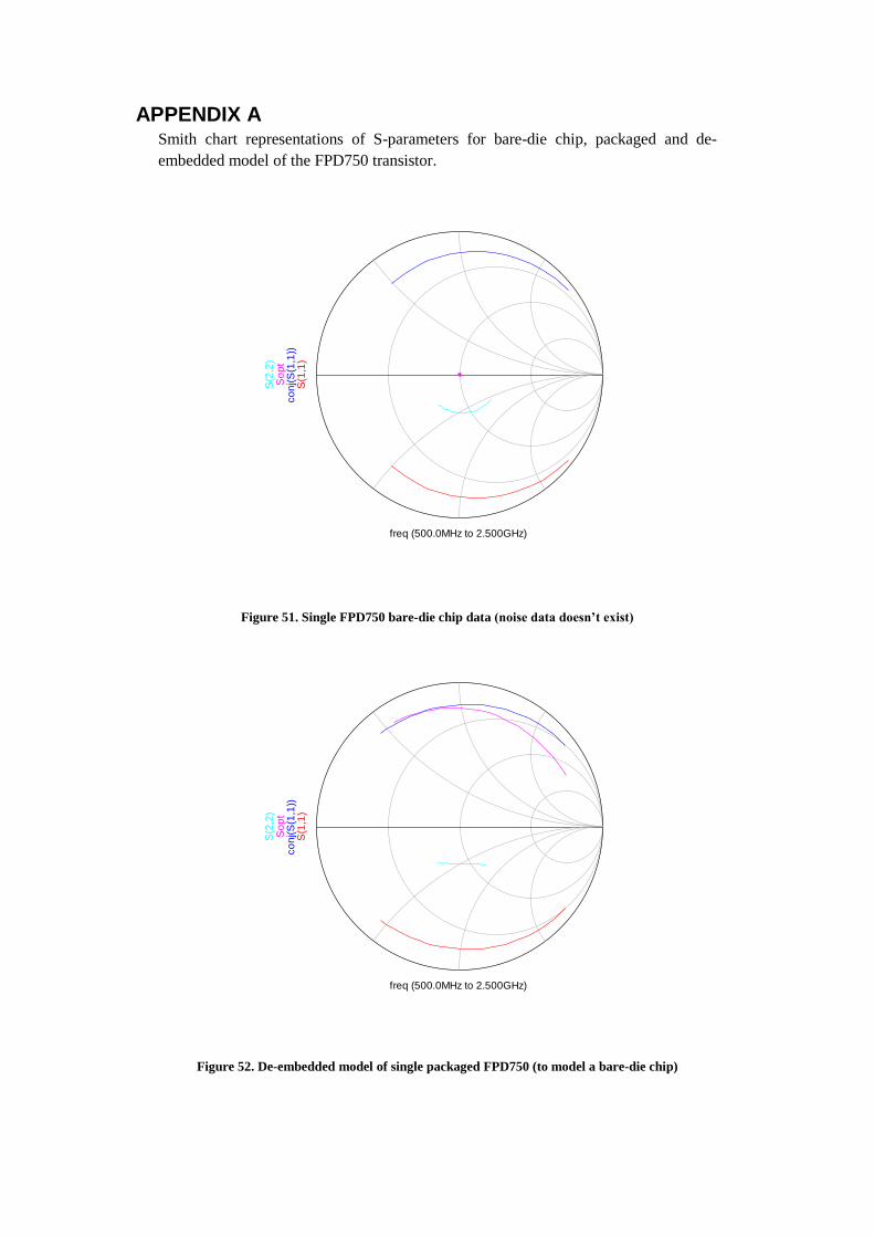
APPENDIX A Smith chart representations of S-parameters for bare-die chip, packaged and de-
embedded model of the FPD750 transistor.
Figure 51. Single FPD750 bare-die chip data (noise data doesn’t exist)
Figure 52. De-embedded model of single packaged FPD750 (to model a bare-die chip)
freq (500.0MHz to 2.500GHz)
S(1
,1)
co
nj(S
(1,1
))S
op
tS
(2,2
)
freq (500.0MHz to 2.500GHz)
S(1
,1)
co
nj(S
(1,1
))S
op
tS
(2,2
)
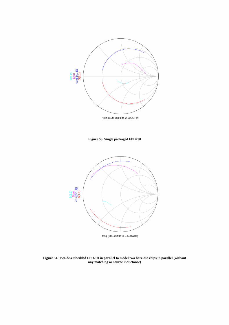
Figure 53. Single packaged FPD750
Figure 54. Two de-embedded FPD750 in parallel to model two bare-die chips in parallel (without
any matching or source inductance)
freq (500.0MHz to 2.500GHz)
S(1
,1)
co
nj(S
(1,1
))S
op
tS
(2,2
)
freq (500.0MHz to 2.500GHz)
S(1
,1)
co
nj(S
(1,1
))S
op
tS
(2,2
)
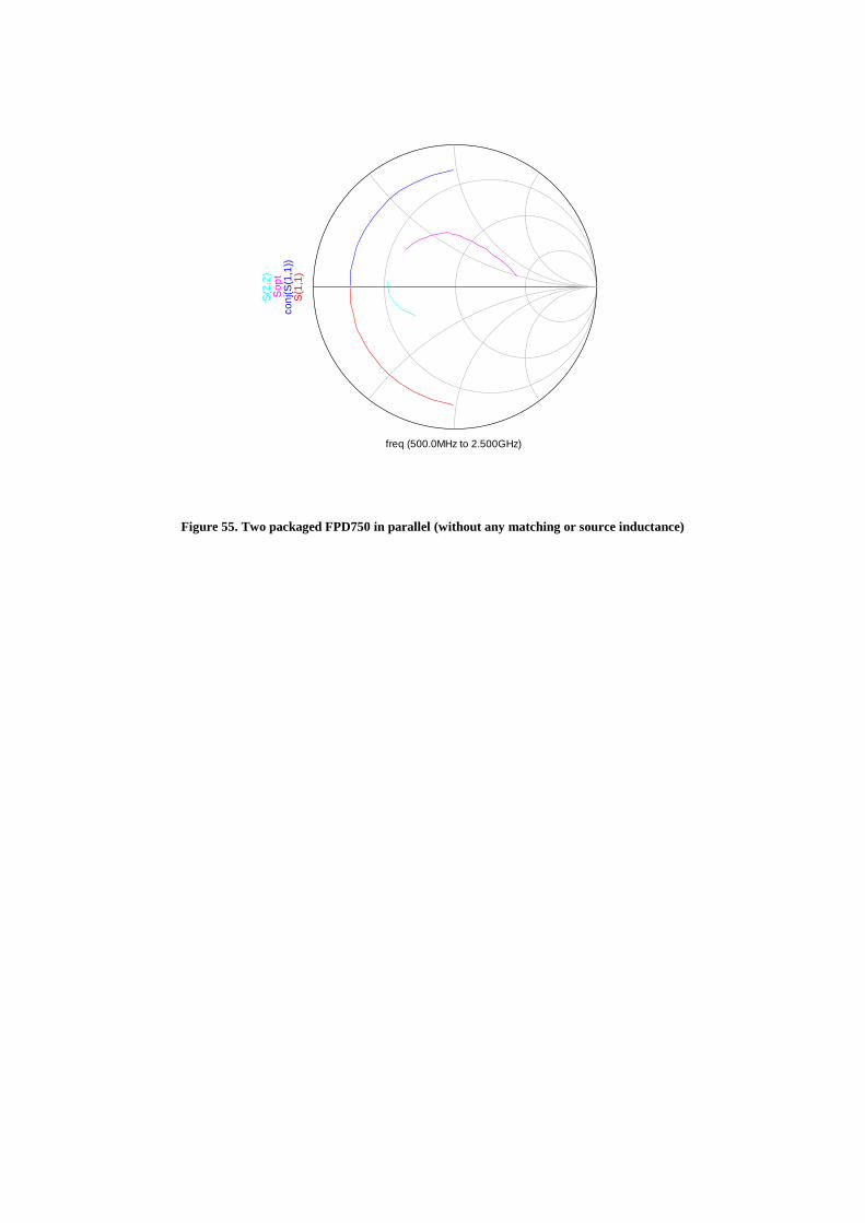
Figure 55. Two packaged FPD750 in parallel (without any matching or source inductance)
freq (500.0MHz to 2.500GHz)
S(1
,1)
co
nj(S
(1,1
))S
op
tS
(2,2
)

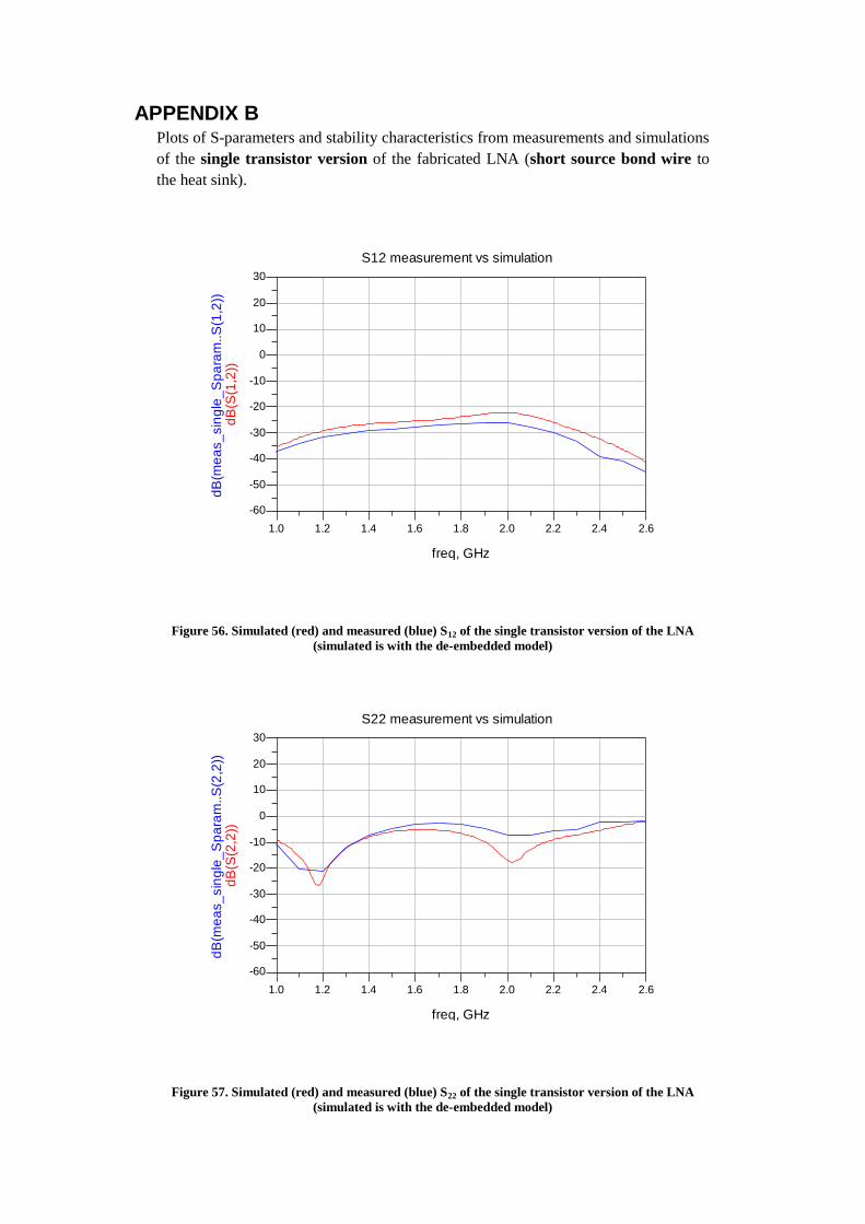
APPENDIX B Plots of S-parameters and stability characteristics from measurements and simulations
of the single transistor version of the fabricated LNA (short source bond wire to
the heat sink).
Figure 56. Simulated (red) and measured (blue) S12 of the single transistor version of the LNA
(simulated is with the de-embedded model)
Figure 57. Simulated (red) and measured (blue) S22 of the single transistor version of the LNA
(simulated is with the de-embedded model)
1.2 1.4 1.6 1.8 2.0 2.2 2.41.0 2.6
-50
-40
-30
-20
-10
0
10
20
-60
30
freq, GHz
dB
(S(1
,2))
dB
(me
as_
sin
gle
_S
pa
ram
..S
(1,2
))
S12 measurement vs simulation
1.2 1.4 1.6 1.8 2.0 2.2 2.41.0 2.6
-50
-40
-30
-20
-10
0
10
20
-60
30
freq, GHz
dB
(S(2
,2))
dB
(me
as_
sin
gle
_S
pa
ram
..S
(2,2
))
S22 measurement vs simulation
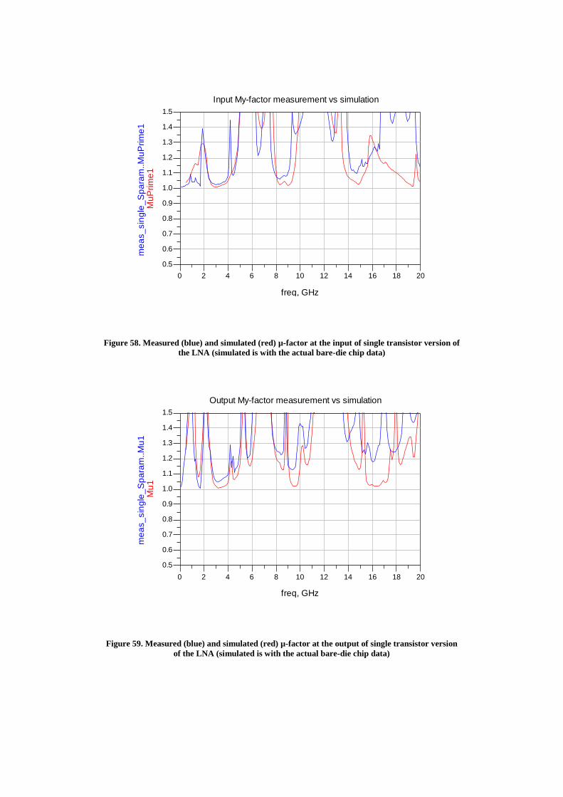
Figure 58. Measured (blue) and simulated (red) µ-factor at the input of single transistor version of
the LNA (simulated is with the actual bare-die chip data)
Figure 59. Measured (blue) and simulated (red) µ-factor at the output of single transistor version
of the LNA (simulated is with the actual bare-die chip data)
2 4 6 8 10 12 14 16 180 20
0.6
0.7
0.8
0.9
1.0
1.1
1.2
1.3
1.4
0.5
1.5
freq, GHz
Mu
Prim
e1
me
as_
sin
gle
_S
pa
ram
..M
uP
rim
e1
Input My-factor measurement vs simulation
2 4 6 8 10 12 14 16 180 20
0.6
0.7
0.8
0.9
1.0
1.1
1.2
1.3
1.4
0.5
1.5
freq, GHz
Mu
1m
ea
s_
sin
gle
_S
pa
ram
..M
u1
Output My-factor measurement vs simulation
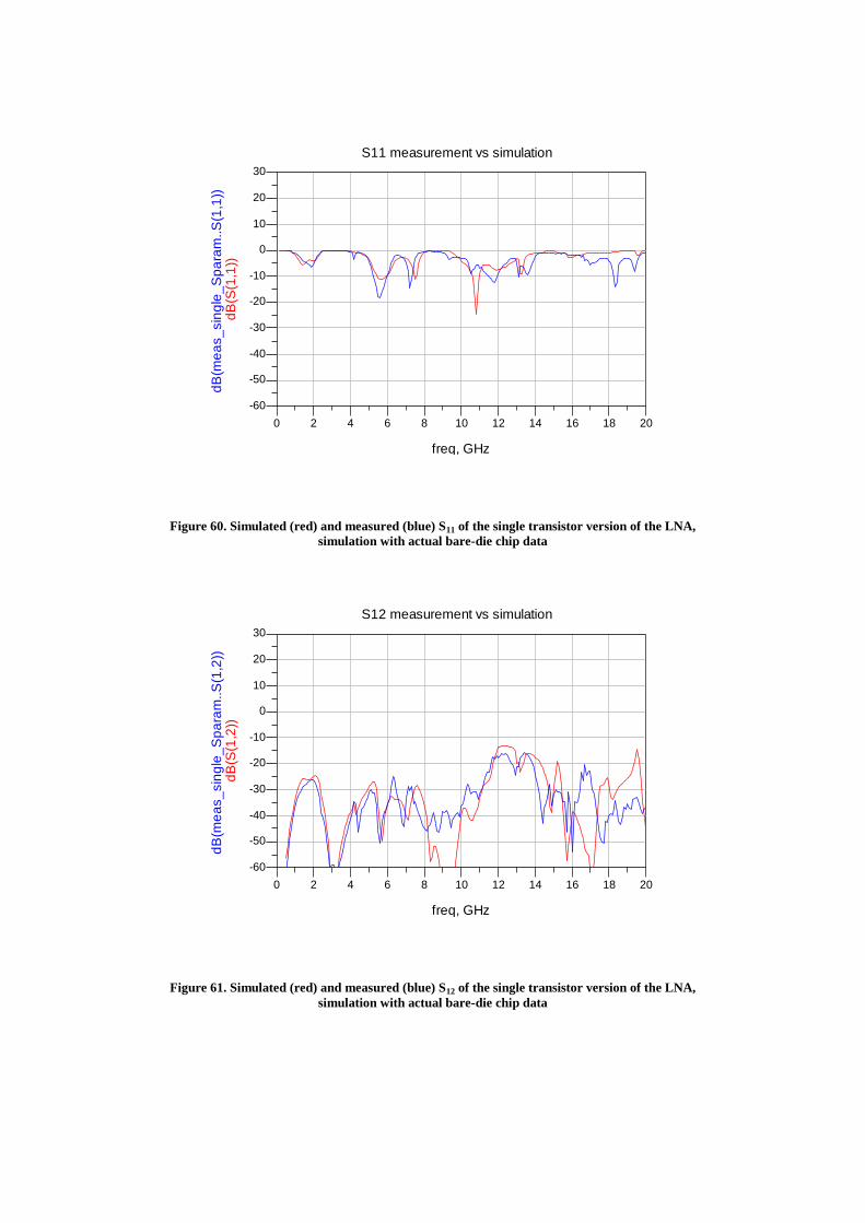
Figure 60. Simulated (red) and measured (blue) S11 of the single transistor version of the LNA,
simulation with actual bare-die chip data
Figure 61. Simulated (red) and measured (blue) S12 of the single transistor version of the LNA,
simulation with actual bare-die chip data
2 4 6 8 10 12 14 16 180 20
-50
-40
-30
-20
-10
0
10
20
-60
30
freq, GHz
dB
(S(1
,1))
dB
(me
as_
sin
gle
_S
pa
ram
..S
(1,1
))
S11 measurement vs simulation
2 4 6 8 10 12 14 16 180 20
-50
-40
-30
-20
-10
0
10
20
-60
30
freq, GHz
dB
(S(1
,2))
dB
(me
as_
sin
gle
_S
pa
ram
..S
(1,2
))
S12 measurement vs simulation
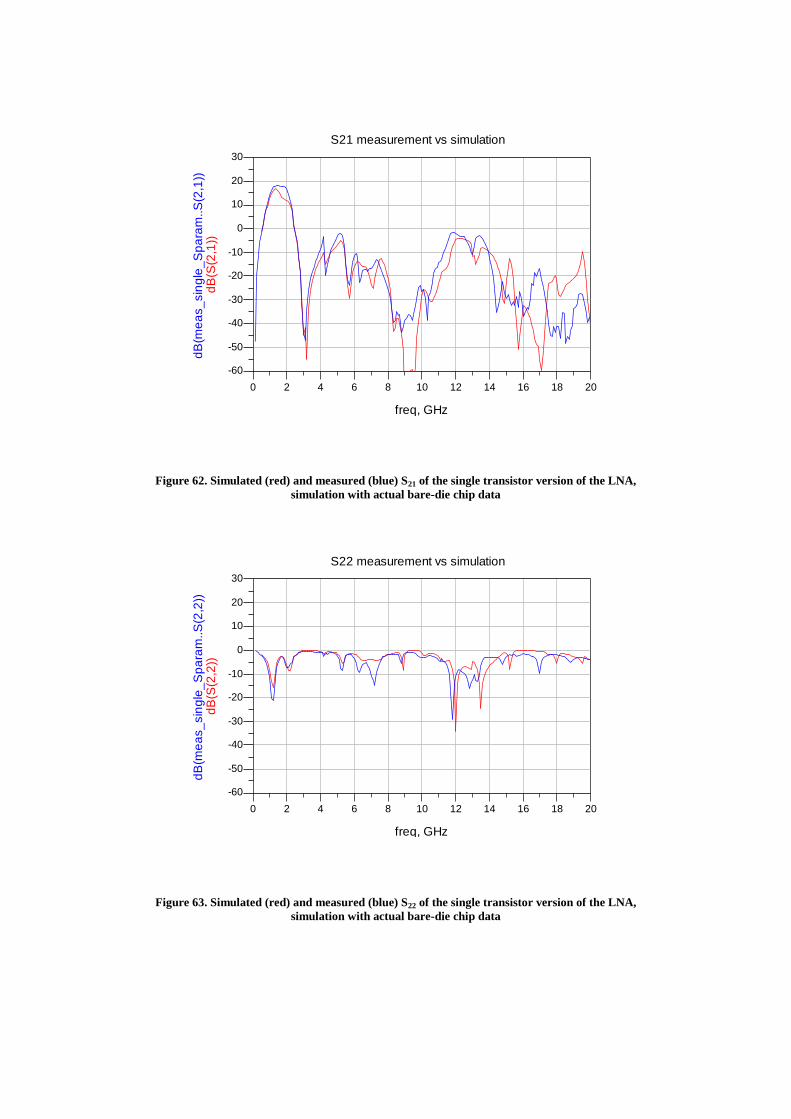
Figure 62. Simulated (red) and measured (blue) S21 of the single transistor version of the LNA,
simulation with actual bare-die chip data
Figure 63. Simulated (red) and measured (blue) S22 of the single transistor version of the LNA,
simulation with actual bare-die chip data
2 4 6 8 10 12 14 16 180 20
-50
-40
-30
-20
-10
0
10
20
-60
30
freq, GHz
dB
(S(2
,1))
dB
(me
as_
sin
gle
_S
pa
ram
..S
(2,1
))
S21 measurement vs simulation
2 4 6 8 10 12 14 16 180 20
-50
-40
-30
-20
-10
0
10
20
-60
30
freq, GHz
dB
(S(2
,2))
dB
(me
as_
sin
gle
_S
pa
ram
..S
(2,2
))
S22 measurement vs simulation
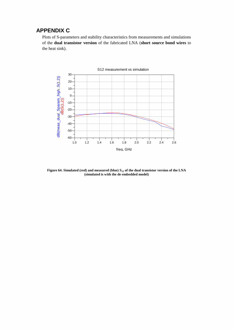
APPENDIX C Plots of S-parameters and stability characteristics from measurements and simulations
of the dual transistor version of the fabricated LNA (short source bond wires to
the heat sink).
Figure 64. Simulated (red) and measured (blue) S12 of the dual transistor version of the LNA
(simulated is with the de-embedded model)
1.2 1.4 1.6 1.8 2.0 2.2 2.41.0 2.6
-50
-40
-30
-20
-10
0
10
20
-60
30
freq, GHz
dB
(S(1
,2))
dB
(me
as_
du
al_
Sp
ara
m_
hig
h..S
(1,2
))
S12 measurement vs simulation
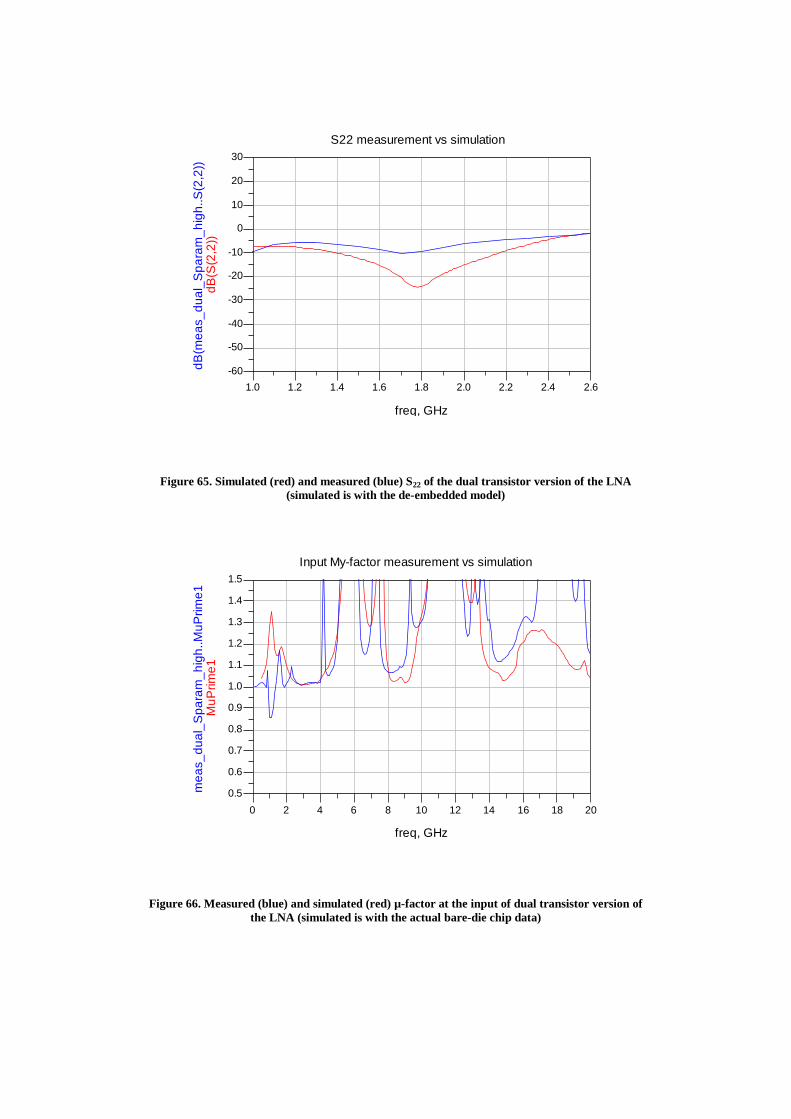
Figure 65. Simulated (red) and measured (blue) S22 of the dual transistor version of the LNA
(simulated is with the de-embedded model)
Figure 66. Measured (blue) and simulated (red) µ-factor at the input of dual transistor version of
the LNA (simulated is with the actual bare-die chip data)
1.2 1.4 1.6 1.8 2.0 2.2 2.41.0 2.6
-50
-40
-30
-20
-10
0
10
20
-60
30
freq, GHz
dB
(S(2
,2))
dB
(me
as_
du
al_
Sp
ara
m_
hig
h..S
(2,2
))
S22 measurement vs simulation
2 4 6 8 10 12 14 16 180 20
0.6
0.7
0.8
0.9
1.0
1.1
1.2
1.3
1.4
0.5
1.5
freq, GHz
Mu
Prim
e1
me
as_
du
al_
Sp
ara
m_
hig
h..M
uP
rim
e1
Input My-factor measurement vs simulation
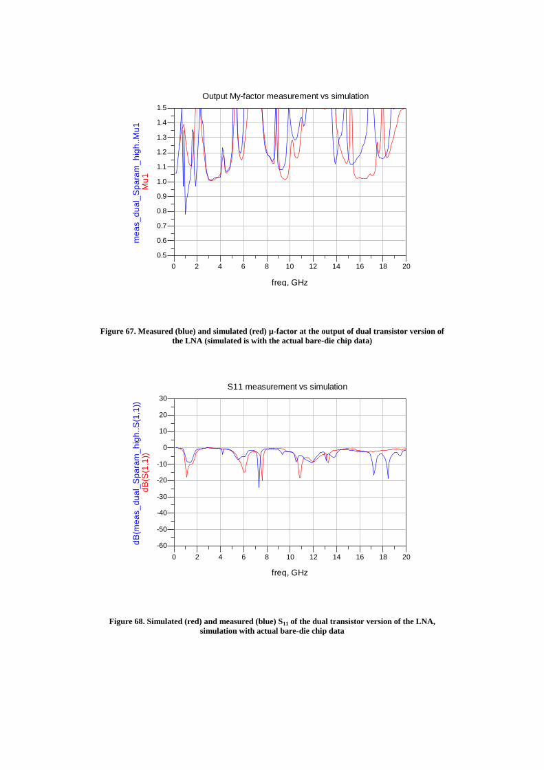
Figure 67. Measured (blue) and simulated (red) µ-factor at the output of dual transistor version of
the LNA (simulated is with the actual bare-die chip data)
Figure 68. Simulated (red) and measured (blue) S11 of the dual transistor version of the LNA,
simulation with actual bare-die chip data
2 4 6 8 10 12 14 16 180 20
0.6
0.7
0.8
0.9
1.0
1.1
1.2
1.3
1.4
0.5
1.5
freq, GHz
Mu
1m
ea
s_
du
al_
Sp
ara
m_
hig
h..M
u1
Output My-factor measurement vs simulation
2 4 6 8 10 12 14 16 180 20
-50
-40
-30
-20
-10
0
10
20
-60
30
freq, GHz
dB
(S(1
,1))
dB
(me
as_
du
al_
Sp
ara
m_
hig
h..S
(1,1
))
S11 measurement vs simulation
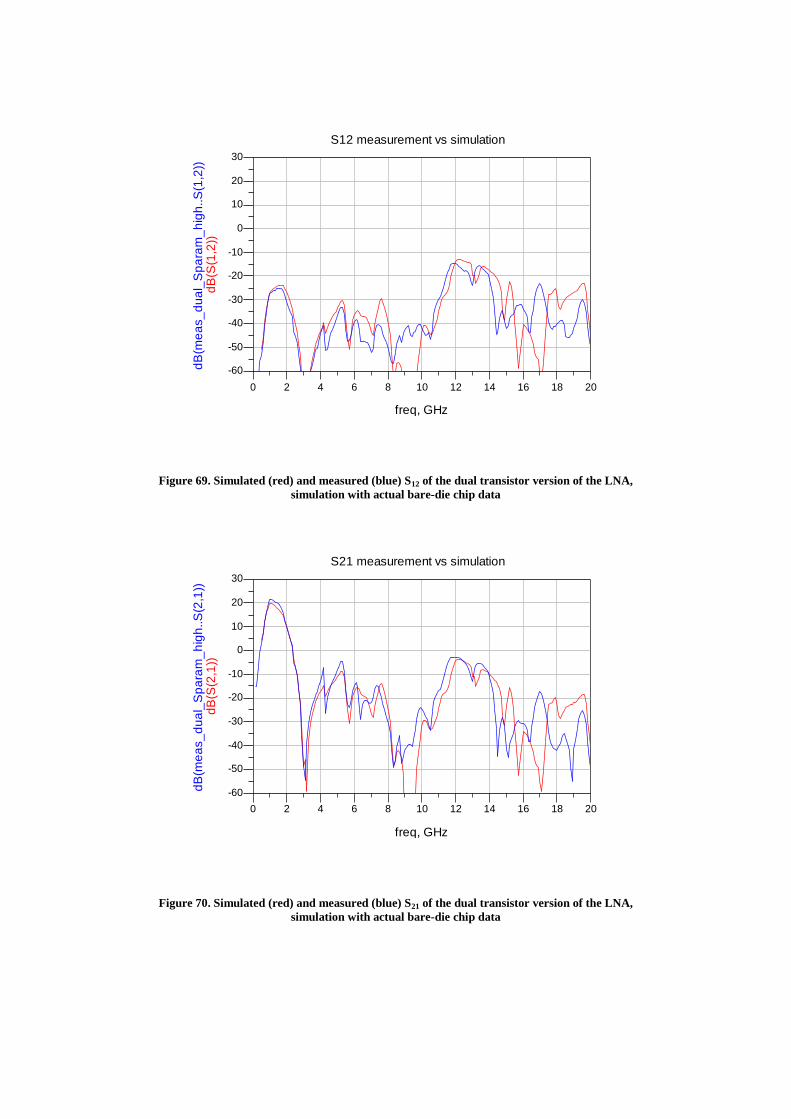
Figure 69. Simulated (red) and measured (blue) S12 of the dual transistor version of the LNA,
simulation with actual bare-die chip data
Figure 70. Simulated (red) and measured (blue) S21 of the dual transistor version of the LNA,
simulation with actual bare-die chip data
2 4 6 8 10 12 14 16 180 20
-50
-40
-30
-20
-10
0
10
20
-60
30
freq, GHz
dB
(S(1
,2))
dB
(me
as_
du
al_
Sp
ara
m_
hig
h..S
(1,2
))
S12 measurement vs simulation
2 4 6 8 10 12 14 16 180 20
-50
-40
-30
-20
-10
0
10
20
-60
30
freq, GHz
dB
(S(2
,1))
dB
(me
as_
du
al_
Sp
ara
m_
hig
h..S
(2,1
))
S21 measurement vs simulation
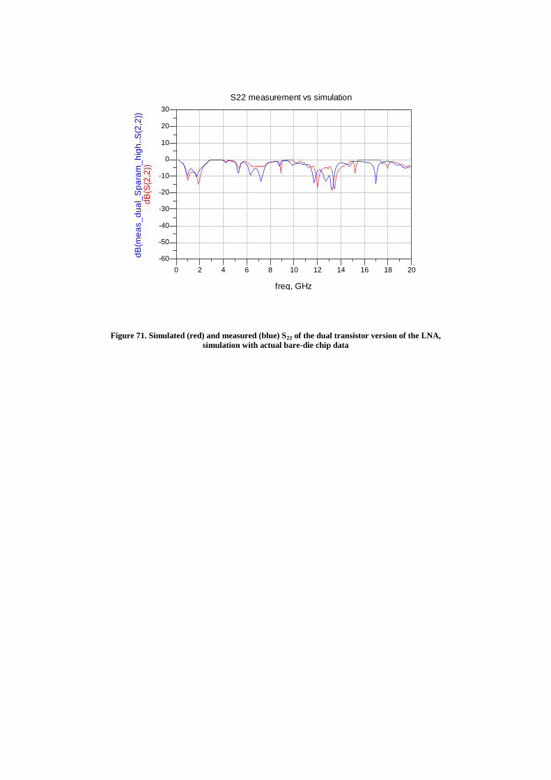
Figure 71. Simulated (red) and measured (blue) S22 of the dual transistor version of the LNA,
simulation with actual bare-die chip data
2 4 6 8 10 12 14 16 180 20
-50
-40
-30
-20
-10
0
10
20
-60
30
freq, GHz
dB
(S(2
,2))
dB
(me
as_
du
al_
Sp
ara
m_
hig
h..S
(2,2
))
S22 measurement vs simulation
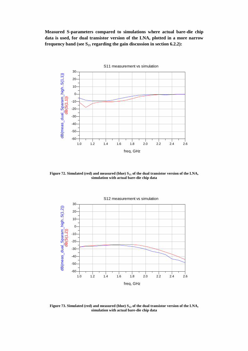
Measured S-parameters compared to simulations where actual bare-die chip
data is used, for dual transistor version of the LNA, plotted in a more narrow
frequency band (see S21 regarding the gain discussion in section 6.2.2):
Figure 72. Simulated (red) and measured (blue) S11 of the dual transistor version of the LNA,
simulation with actual bare-die chip data
Figure 73. Simulated (red) and measured (blue) S12 of the dual transistor version of the LNA,
simulation with actual bare-die chip data
1.2 1.4 1.6 1.8 2.0 2.2 2.41.0 2.6
-50
-40
-30
-20
-10
0
10
20
-60
30
freq, GHz
dB
(S(1
,1))
dB
(me
as_
du
al_
Sp
ara
m_
hig
h..S
(1,1
))
S11 measurement vs simulation
1.2 1.4 1.6 1.8 2.0 2.2 2.41.0 2.6
-50
-40
-30
-20
-10
0
10
20
-60
30
freq, GHz
dB
(S(1
,2))
dB
(me
as_
du
al_
Sp
ara
m_
hig
h..S
(1,2
))
S12 measurement vs simulation
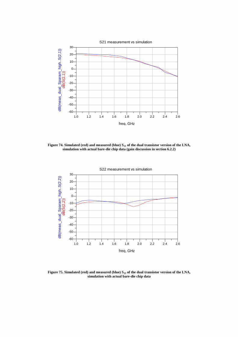
Figure 74. Simulated (red) and measured (blue) S21 of the dual transistor version of the LNA,
simulation with actual bare-die chip data (gain discussion in section 6.2.2)
Figure 75. Simulated (red) and measured (blue) S22 of the dual transistor version of the LNA,
simulation with actual bare-die chip data
1.2 1.4 1.6 1.8 2.0 2.2 2.41.0 2.6
-50
-40
-30
-20
-10
0
10
20
-60
30
freq, GHz
dB
(S(2
,1))
dB
(me
as_
du
al_
Sp
ara
m_
hig
h..S
(2,1
))
S21 measurement vs simulation
1.2 1.4 1.6 1.8 2.0 2.2 2.41.0 2.6
-50
-40
-30
-20
-10
0
10
20
-60
30
freq, GHz
dB
(S(2
,2))
dB
(me
as_
du
al_
Sp
ara
m_
hig
h..S
(2,2
))
S22 measurement vs simulation