Embed Size (px)
Citation preview

CARBON BASED SMART SYSTEM FOR WIRELESS APPLICATION
Start Date : 01/09/12 Project n° 318352 Duration : 45 months Topic addressed : Very advanced nanoelectronic comp onents: design, engineering, technology and manufacturability
WORK PACKAGE 7 : Project management
DELIVERABLE D7.18
Progress Activity Report #4 Covered period: T0+18 – T0+24
Due date : T0+24 Submission date : T0+33
Lead contractor for this deliverable: TRT
Dissemination level : PU – Public

D7.18 - Progress Activity Report #4 (T0+18 – T0+24)
2/35
2
WORK PACKAGE 7: Project management
PARTNERS ORGANISATION APPROVAL
Name Function Date Signature
Prepared by: S.Xavier R&D Engineer 22/06/15
Approved by: Afshin Ziaei Research Program Manager
22/06/15
DISTRIBUTION LIST
QUANTITY ORGANIZATION NAMES
1 ex Thales Research and Technology TRT Afshin ZIAEI
1 ex Chalmers University of Technology CHALMERS Johan LIU
1 ex Foundation for Research & Technology - Hellas FORTH George KONSTANDINIS
1 ex Laboratoire d’Architecture et d’Analyse des Systèmes
CNRS-LAAS Patrick PONS
1 ex Université Pierre et Marie Curie UPMC Charlotte TRIPON-CANSELIET
1 ex National Research and Development Institute for Microtechnologies
IMT Mircea DRAGOMAN
1 ex Graphene Industries GI Peter BLAKE
1 ex Thales Systèmes Aéroportés TSA Yves MANCUSO
1 ex SHT Smart High-Tech AB SHT Yifeng FU
1 ex Universita politecnica delle Marche UNIVPM Luca PIERANTONI
1 ex Linköping University LiU Rositsa YAKIMOVA
1 ex Fundacio Privada Institute Catala de Nanotecnologia
ICN Clivia SOTOMAYOR
1 ex Tyndall-UCC Tyndall Mircea MODREANU

D7.18 - Progress Activity Report #4 (T0+18 – T0+24)
3/35
3
CHANGE RECORD SHEET
REVISION LETTER DATE PAGE NUMBER DESCRIPTION
v0 07/2013 10 Initial version
v1 24/09/2014 30 All partners contributions
v2 31//10/2014 34 Final version
V3 22/06/2015 35 Correction after 2nd review meeting

D7.18 - Progress Activity Report #4 (T0+18 – T0+24)
4/35
4
CONTENTS
1 PROJECT OBJECTIVES AND MAJOR ACHIEVEMENTS DURING RE PORTING PERIOD (T0+18 – T0+24) 7
1.1 PROJECT OBJECTIVES DURING THE REPORTING PERIOD (T0+18-T0+24) 7
1.2 MAJOR ACHIEVEMENTS DURING THE REPORTING PERIOD (T0+18-T0+24) 8
1.2.1 WP2 : Design and simulation activities 8
1.2.2 WP3 : Fabrication activities 8
1.2.3 WP4 : Test activities 9
1.2.4 WP6 : Dissemination and exploitation activities 9
1.2.5 WP7 : Management activities 9
2 MANAGEMENT ACTIVITIES (WP7) 9
2.1 MEETING 9
3 PROGRESS IN THE ACTIVE THECNICAL WORKPACKAGE 2 10
3.1 WP2 : DESIGN AND SIMULATION ACTIVITIES 10
3.1.1 WP OBJECTIVES 10
3.1.2 PROGRESS TOWARD OBJECTIVES : STATUS OF ACTIVES TASKS 10
3.1.2.1 Task 2.1: Design of the CNT FET (FORTH/IMT) 10
3.1.2.2 Task 2.3 : Design of the CNT filter/oscillator (LAAS/IMT) 11
3.1.2.1 Task 2.5 : Design and simulation of RF grapheme devices (UNIVPM/FORTH) 13
4 PROGRESS IN THE ACTIVE THECNICAL WORKPACKAGE 3 14
4.1 WP3 : FABRICATION ACTIVITIES 14
4.2 WP OBJECTIVES 14
4.2.1 PROGRESS TOWARD OBJECTIVES : STATUS OF ACTIVES TASKS 15
4.2.1.1 Task.3.1 CNT and graphene growth technology 15
4.2.1.2 Task.3.2 CNT and graphene material characterization 19
4.2.1.3 Task.3.3 Fabrication of CNT FET 21
4.2.1.4 Task.3.4 CNT RF switch fabrication (TRT) 21
4.2.1.5 Task.3.6 CNT based antenna fabrication (TRT/SHT/UPMC) 22
4.2.1.6 Task.3.7 Development of carbon nanotube interconnects (SHT/CHALMERS) 23
4.2.1.7 Task.3.8 Development of RF graphene devices 24
5 PROGRESS IN THE ACTIVE THECNICAL WORKPACKAGE 4 28
5.1 WP4 : TEST ACTIVITIES 28
5.2 WP OBJECTIVES 28
5.3 PROGRESS TOWARD OBJECTIVES : STATUS OF ACTIVES TASKS 28
5.3.1 Task.4.1 CNT and graphene FET tests 28
5.3.2 Task.4.4 CNT and graphene based antenna tests 29
6 DISSEMINATION AND EXPLOITATION ACTIVITIES (WP6) 32
6.1 PUBLICATIONS & CONFERENCE 32

D7.18 - Progress Activity Report #4 (T0+18 – T0+24)
5/35
5
FIGURES Figure 1 : NANO-RF Timetable ............................................................................................................ 8
Figure 2 : Layers used during fabrication and their details ................................................................. 10
Figure 3 : 3D images of one of the simulated devices (top) and their corresponding RF performance (bottom). It is verified that the designed FETs are gate capacitance limited. The output port is resistance governed. ................................................................................................................... 11
Figure 4 : CST MWS final design of the: a) whole filter; b) single spiral inductor-varactor branch ..... 12
Figure 5 : CST MWS final design of the: a) whole filter; b) single meandered inductor-varactor branch .................................................................................................................................................... 12
Figure 6 : The tunability of the cNT filter as a functionon of applied DC on CNT varactor. ................. 13
Figure 7 : Increasing the gate voltage, charge transmittivity increases (green) and reflectivity reduces (blue). .......................................................................................................................................... 14
Figure 8 : CNTs horizontally growth using growth optimized condition ............................................... 16
Figure 9 : Newly constructed etching-growth system under operation conditions. ............................. 17
Figure 10 : AFM phase contrast images: Graphene grown at a) high and b) low Argon pressure. Darker area is 2 ML. ........................................................................................................................................... 17
Figure 11 : AFM phase contrast image. Argon is let in the growth cell at 1200oC. White patches are 2MLs. .......................................................................................................................................... 18
Figure 12 : AFM images in different modes taken from a) clean graphene surface and after appearance of adsorbates. .......................................................................................................... 18
Figure 13 : The single layer graphene coverage of SiC: samples G480 and G481 supplied by partner Linköping University .................................................................................................................... 20
Figure 14 : Horizontally aligned CNTs grown on quartz substrate ...................................................... 21
Figure 15 : AFM scanning of SWCNTs grown on quartz substrate .................................................... 21
Figure 16 : Fabrication of CNTs RF switch ........................................................................................ 22
Figure 17 : Generic layout for CNT-based monopole in CPW technology (HR Si and quartz substrate) .................................................................................................................................................... 22
Figure 18 : CNTs antenna fabrication and growth .............................................................................. 23
Figure 20 : 0.2µm wide gate deposited in a 0.6µm wide Source – Drain distance. Note that the source drain is beyond the specification put forward by the optical lithography and the resist used. ....... 25
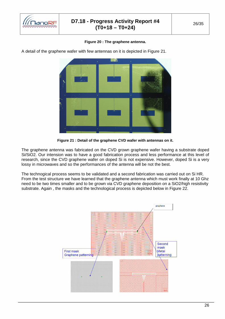
Figure 21 : The graphene antenna..................................................................................................... 26
Figure 22 : Detail of the graphene CVD wafer with antennas on it. .................................................... 26
Figure 23 : The graphene antenna on high resistivity Si. ................................................................... 27
Figure 24 : Proposed antenna configurations for biasing the graphene. ............................................ 27
Figure 25 : Graphene antenna on high resistivity Si. .......................................................................... 27
Figure 26: Low access resistance (<6 Ohms) and the Dirac point accessible by gate voltage from devices fabricated on Graphene consortium material (SiC). ........................................................ 28
Figure 27 : Previous generation of graphene FET have been characterised in RF. Maximum stable gain in embedded data is shown. ................................................................................................ 29
Figure 28 : Source – drain current of a CNTFET with 4µm S-D distance and its respective transconductance verifying that that operates as a normally off device ....................................... 29
Figure 29 : S11 for the graphene antenna ......................................................................................... 30
Figure 30 : The simulated radition pattern.......................................................................................... 31
Figure 31 : S11 of the graphene antenna on Si.high resistivity .......................................................... 31
Figure 32 : S21 and gain of graphene antenna on high resistivity Si substrate. ................................. 32

D7.18 - Progress Activity Report #4 (T0+18 – T0+24)
6/35
6
TABLES Table 1 : Information about the graphene flakes produced during the last 6 month ........................... 19
Table 2 : Single layer graphene coverage of SiC (LiU) as determined from high-resolution, large area MicroRaman mapping measurements ......................................................................................... 20
Table 3: Table of specific contact resistivity measured on graphene contacts ................................... 25

D7.18 - Progress Activity Report #4 (T0+18 – T0+24)
7/35
7
1 PROJECT OBJECTIVES AND MAJOR ACHIEVEMENTS DURING REPORTING PERIOD (T0+18 – T0+24)
1.1 PROJECT OBJECTIVES DURING THE REPORTING PERIOD (T0+18-T0+24)
According to the timetable (see Figure 1), the project objectives over the reporting period are:
• Within the framework of WP 2 ‘Design and simulation activities’ : according to the first review
meeting, the work for WP2 continues in parallel of WP3 during the second year of the project
• Within the framework of WP 3 ‘Fabrication activities’ to: all the CNT and graphene based sub-modules that have been designed in the work package 2. The principal objective of this work package is to fabricate the test structures and also final components based on the results of WP2
• Within the framework of WP 4 ‘Test activities’: the different manufactured CNT components will be tested, consisting of the following test:
CNT FET and graphene electrical characterization: DC to RF o CNT RF switch tests o CNT based filter/oscillator tests§ CNT based antenna tests o RF graphene device (LNA ,mixer, detector) o Calibration of basic equivalent circuit models (parameter extraction based on
experimental data)
• Within the framework of WP 6 ‘Dissemination and exploitation activities : dissemination information and results of the project within the partners and youside the project, as well as proposing exploitation transfer plans and managing the Intellectual
List of publication and conference Explotation activities
• Within the framework of WP 7 ‘Project Management’ : to establish durable basis for the
project management and monitoring all along the project duration, through the following actions:
Regular project and technical meetings;
As described in the following sections, all these objectives have progressed between T0+18 and T0+24.

D7.18 - Progress Activity Report #4 (T0+18 – T0+24)
8/35
8
Figure 1 : NANO-RF Timetable
1.2 MAJOR ACHIEVEMENTS DURING THE REPORTING PERIOD (T0+18-T0+24)
1.2.1 WP2 : Design and simulation activities In the reporting period (T0+18-T0+24), different devices of the project have been redesigned:
- CNT Filters - CNT FET - Design and simulation of RF graphene devices
Mask necessary for the fabrication has been also designed after strong collaboration with WP3 (to take account the technological constraint.
1.2.2 WP3 : Fabrication activities Regarding the development of the technology for the CNT and graphene growth, some achievements have been obtained:
- CNT growth condition optimization for CNT switch and filter - Improvement of density for the horizontally aligned SWCNT for CNT FET - Improvement of the quality of CVD graphene after growth condition modification - Better understanding of the role of bilayer inclusion (their percentage decrease to 3.5%)
and in house optical characterization for grahene on SiC - Expansion of the SiC graphene area (20x20mm²)

D7.18 - Progress Activity Report #4 (T0+18 – T0+24)
9/35
9
Several CNT and graphene samples are also prepared and delivered to the consortium. During the period, some devices have been also fabricated:
- A process flow has been established for the realization of RF NEMS devices compatible with the high temperature of the CNTs growth. Using this process flow, first RF NEMS f have been fabricated
- Following the design determined for the CNTs antenna, the first CNTs antenna has been fabricated. The first tests showed that the CNTs diameter to length ratio is critical.
- Development of the stacking process to enable multi-layer 3D interconnect structure using CNT bundles
- Optimization of the dielectric layer (HfO2) deposition on graphene - Fist fabrication of graphene FET and graphene antenna
1.2.3 WP4 : Test activities The different manufactured CNT components fabricated in WP3 are measured:
Electrical characterization (DC to RF) for CNT FET CNT based antenna tests Calibration of basic equivalent circuit models (parameter extraction based on experimental
data)
1.2.4 WP6 : Dissemination and exploitation activiti es During the period reported, Nano-RF workshop was organized at Rome during the European microwave conference 2014. There are also several publication and conference.
1.2.5 WP7 : Management activities During the period several meeting were organized :
- 2 project meetings, where all the partners are represented - 2 technical meetings for WP 3, where only the partners involved in the given WP are
represented
2 MANAGEMENT ACTIVITIES (WP7)
WP leader Involved Partners
Duration Deliverables Milestones
Active Tasks Status
TRT
TRT, CHALMERS,
FORTH, LAAS, IMT, TSA,
SHT, UNIVPM, ICN, Tyndall
T0 – T0+36 D7.1 to D7.21 M7.1 - On-Going
2.1 MEETING In order to ensure a correct progress and a high coherence of the collaborative project, during the reporting period, numerous meetings were organized: 2 project meetings, where all the partners are represented
o 18-Month Meeting, held in Bucharest on 27th May 2014;

D7.18 - Progress Activity Report #4 (T0+18 – T0+24)
10/35
10
o 24-Month Meeting, held in Ancona on 17th September 2014;
2 technical meetings for WP 3, where only the partners involved in the given WP are represented: o Technical Meeting, held in Brussels on 02nd May 2014 and 18th July 2014;
The agendas, minutes and presentations made for these meetings are downloadable on the private area of the website.
3 PROGRESS IN THE ACTIVE THECNICAL WORKPACKAGE 2
3.1 WP2 : DESIGN AND SIMULATION ACTIVITIES
WP leader Involved Partners
Duration Deliverables Milestones
Active Tasks Status
IMT
TRT, UPMC, IMT, TSA,
UNIVPM, LiU, ICN
T0 +3 – T0+12 D2.1 to D2.5 M2.1 T2.1 to T2.5 Postpone
All the deliverable for WP2 are submitted at T0+13.
3.1.1 WP OBJECTIVES In this WP, we will design and simulate all the CNTs and graphene based sub-components forming the nano T/R module to be demonstrated in WP5 comprising filters/oscillators, switches, mixers, LNAs and PAs and finally an antenna. The main technical objectives are:
Design and modeling of CNT and graphene based FET and then design and modeling of LNA, PA and mixer based on either CNT or graphene
Design and modeling of CNT switch Design and modeling of CNT filter/oscillator and graphene mixer Design and modeling of CNT antenna Design and modeling of LNA based graphene Design and modeling of a graphene loaded antenna.
3.1.2 PROGRESS TOWARD OBJECTIVES : STATUS OF ACTIVE S TASKS
3.1.2.1 Task 2.1: Design of the CNT FET (FORTH/IMT) FET devices defined in the last mask set designed in LAAS were simulated using Agilent ADS and their RF performance was studied.
Figure 2 : Layers used during fabrication and their details

D7.18 - Progress Activity Report #4 (T0+18 – T0+24)
11/35
11
Figure 2 shows the layers used. The technology finalized permits fabrication of capacitors and inductors that will enable the complete circuits to be fabricated.
Figure 3 shows the simulation result of the CNT FET device.
Figure 3 : 3D images of one of the simulated device s (top) and their corresponding RF performance (bottom). It is verified that the designed FETs are gate capacitance limited. The output port is resis tance governed.
3.1.2.2 Task 2.3 : Design of the CNT filter/oscillator (LAAS/IMT) In this task, we have designed two distinct configurations of filters based CNT having the following prerequisites: 1. Resonance frequency in the 8-12GHz band; 2. Exploitation of carbon nanotubes for designing a variable capacitor (varactor). We have also designed their associated masks according to fabrication process. The two design are described in Figure 4 and Figure 5

D7.18 - Progress Activity Report #4 (T0+18 – T0+24)
12/35
12
(a) (b) Figure 4 : CST MWS final design of the: a) whole fi lter; b) single spiral inductor-varactor branch
(a) (b) Figure 5 : CST MWS final design of the: a) whole fi lter; b) single meandered inductor-varactor branch
We have considered two different inductor layouts: a spiral inductor with air bridge (Figure 4). We will refer to this solution as solution #1; a meandered inductor (Figure 5). We will refer to this solution as solution #2. The two solutions provide different filtering properties in the band of interest, since the inductance and the overall electromagnetic effects change. This two solutions were chosen by the following reasons :
-solution # 1: the spiral inductor is high Q inductor, but the technological process implies 6 masks, 5 masks are based on optical lithography for L, C realization and the other one is based on e-beam lithography for CNT growth )and rather elaborated technological step to get the CNT filter

D7.18 - Progress Activity Report #4 (T0+18 – T0+24)
13/35
13
-solution #2 : the meander inductor implies a technological process of only two masks ( one mask is based on optical lithography for L,C realization and the other one is based on e-beam lithography for CNT growth.
The CNT-based varactor is in the form of an interdigitated (IDT) structure, whose electrodes (350 nm-wide digits made of 50 nm-thick molybdenum – Mo –) are used to grow the vertical CNTs with a diameter of 100 nm and a height of 2 µm. The usage of Mo is necessary due to its high melting temperature (2620 °C or 2893.15 K). The drawback is that Mo is not a conductor as good as gold, in fact it has a conductivity σMo = 1.82x10⁷ S/m vs. σAu = 4.561x10⁷ S/m, hence σAu = 2.5*σMo. It means that Mo is more lossy than gold and we can expect a little degradation in the filter’s performance. The solution 2 which is simpler to be fabricated displays tunability for the filter parameter as it is shown in Figure 6.
Figure 6 : The tunability of the cNT filter as a fu nctionon of applied DC on CNT varactor.
3.1.2.1 Task 2.5 : Design and simulation of RF grapheme devices (UNIVPM/FORTH)
The present modelling step is aimed at going towards the actual fabricated FET device and taking into account the experimental results, to have and provide reciprocal feedbacks. The starting geometry in shown in Figure 7(a): the transistor is considered as uniform in the x direction. In this case, many electrons can be injected, at different angles, and different energies, into the channel. Figure 7(b) shows transmission of charge in the direction perpendicular to the Source and Drain electrodes (precisely, at an angle of 1° from the perpendicular).

D7.18 - Progress Activity Report #4 (T0+18 – T0+24)
14/35
14
Figure 7 : Increasing the gate voltage, charge tran smittivity increases (green) and reflectivity reduc es (blue). The above calculation is demonstrative, and is preliminary to the final analysis, about the I-V characteristic of the graphene transistor. To this aim, the fabrication data (geometry, material) are being exchanged with FORTH, and parametric analysis is presently being performed.
4 PROGRESS IN THE ACTIVE THECNICAL WORKPACKAGE 3
4.1 WP3 : FABRICATION ACTIVITIES
WP leader Involved Partners
Duration Deliverables Milestones
Active Tasks Status
FORTH
TRT, CHALMERS,
FORTH, LAAS, UPMC, IMT, GI, SHT, LiU, ICN, Tyndall
T0 +3 – T0+25 D3.1 to D3.8 M3.1 T3.1 to T3.10 On Going
D3.1 and D3.2 are submitted at T0+13.
4.2 WP OBJECTIVES In this work package we will fabricate all the CNT and graphene based sub-modules that have been designed in the previous work package. The principal objective of this work package is to fabricate the test structures and also final components based on the results of WP2. The manufacturing

D7.18 - Progress Activity Report #4 (T0+18 – T0+24)
15/35
15
process in this WP will be optimised and the products will be delivered to WP4. The technical objectives for this work package are:
- To develop CNT growth technology to achieve the desired structure following results of the design activities. CNT growth must be compatible with all the substrate technology to achieve the desired RF components as specified in Work-package 1.
- To develop graphene growth techniques either based on exfoliation for proof of concept RF graphene devices and at the wafer scale for graphene circuits to be used in the sub-modules
- To set-up a pilot line for manufacturing CNT for microwave applications.
- To fully characterize the CNT that have been grown by thermal CVD or plasma enhanced CVD . The characterization of graphene via exfoliation or epitaxial growth on SiC. The goal will be to verify that physical, structural, etc. properties will be compatible with the RF functions we want to achieve.
- To fabricate the RF submodules designed in the previous work package: CNT FET (LNA, PA and mixer), the RF switch, the RF filter/oscillator and the antenna, LNA based on graphene, graphene antenna , graphene mixer and graphene detector
- To develop various technologies that will allow for the integration of the sub-modules produced within this work package to be integrated on a single Si carrier wafer.
- To supply other work packages with CNT and graphene for characterization, modeling, simulation and demonstration and to optimize CNT and graphene according to their feedbacks.
4.2.1 PROGRESS TOWARD OBJECTIVES : STATUS OF ACTIVE S TASKS
4.2.1.1 Task.3.1 CNT and graphene growth technology
CNT growth (SHT/TRT)
In the past half year, SHT is focusing on CNT material improvement. We optimized the growth for three applications, the CNT filter/oscillator, the CNT FET and the CNT based RF switch. For filter and FET application, the CNTs are grown by thermal CVD (TCVD) method while for RF switch application the CNTs are grown by plasma enhanced CVD method (PECVD). We tested different growth conditions including catalyst thickness, annealing time and temperature, growth time, gas volume ratio, etc. to improve the quality of CNTs, in particularly for RF switch application since in this case the CNTs are grown on conductive underlayer which will influence the catalyst diffusion and electric field distribution in the CNT growth chamber. More details can be found in D3.5. For CNT growth in the FET application, we also tested different gases for carbon source supply except the optimization of other parameters like in the case of filter and switch. Because in the CNT FET application we need to grow horizontally aligned single-walled CNTs (SWCNTs) for device fabrication, and the substrate and growth conditions as well as the required gas concentration are very different. For example, we used ST-cut quartz substrate rather than Si substrate so that the growth of SWCNTs can follow the crystal direction of the substrate surface. On the other hand, we installed new gas sources in our growth system, because for horizontally aligned SWCNT growth, it is
D7.18 - Progress Activity Report #4 (T0+18 – T0+24)
16/35
16
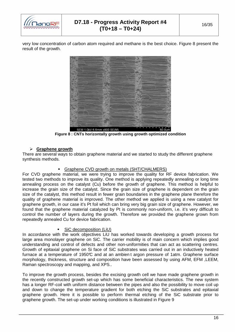
very low concentration of carbon atom required and methane is the best choice. Figure 8 present the result of the growth.
Figure 8 : CNTs horizontally growth using growth op timized condition
Graphene growth There are several ways to obtain graphene material and we started to study the different graphene synthesis methods.
Graphene CVD growth on metals (SHT/CHALMERS) For CVD graphene material, we were trying to improve the quality for RF device fabrication. We tested two methods to improve its quality. One method is applying repeatedly annealing or long time annealing process on the catalyst (Cu) before the growth of graphene. This method is helpful to increase the grain size of the catalyst. Since the grain size of graphene is dependent on the grain size of the catalyst, this method result in fewer grain boundaries in the graphene plane therefore the quality of graphene material is improved. The other method we applied is using a new catalyst for graphene growth, in our case it’s Pt foil which can bring very big grain size of graphene. However, we found that the graphene material catalyzed by Pt is commonly non-uniform, i.e. it’s very difficult to control the number of layers during the growth. Therefore we provided the graphene grown from repeatedly annealed Cu for device fabrication.
SiC decomposition (LiU) In accordance with the work objectives LiU has worked towards developing a growth process for large area monolayer graphene on SiC. The carrier mobility is of main concern which implies good understanding and control of defects and other non-uniformities that can act as scattering centres. Growth of epitaxial graphene on Si face of SiC substrates was carried out in an inductively heated furnace at a temperature of 1950°C and at an ambien t argon pressure of 1atm. Graphene surface morphology, thickness, structure and composition have been assessed by using AFM, EFM ,LEEM, Raman spectroscopy and mapping, and XPS.. To improve the growth process, besides the excising growth cell we have made graphene growth in the recently constructed growth set-up which has some beneficial characteristics. The new system has a longer RF-coil with uniform distance between the pipes and also the possibility to move coil up and down to change the temperature gradient for both etching the SiC substrates and epitaxial graphene growth. Here it is possible to perform thermal etching of the SiC substrate prior to graphene growth. The set-up under working conditions is illustrated in Figure 9

D7.18 - Progress Activity Report #4 (T0+18 – T0+24)
17/35
17
Figure 9 : Newly constructed etching-growth system under operation conditions. By using both growth reactors we have fabricated 25 samples with increasing size in mm2: 7x7 > 10x10 > 15x15 > 20x20. The common tendency observed is that increasing size of the substrate results in increasing percentage of a second graphene layer close to the periphery of the sample. Here we have studied the effect of argon pressure on graphene layer thickness and the thickness uniformity (graphene layer continuity). We have shown that the higher argon pressure result in thinner and more uniform graphene layer (Figure 10a), while with low pressure the thickness can be increase but not uniformly (Figure 10b). The effect of temperature distribution was also studied. For this study we have used a symmetric crucible to have better temperature uniformity and also study the effect of temperature difference in the cell (crucible) on the thickness uniformity. Our preliminary results show that a smaller growth volume improves graphene homogeneity even at low argon pressure. These results contributed to the optimization of the growth process
Figure 10 : AFM phase contrast images: Graphene grown at a) high and b) low Argon pressure. Darker area is 2 ML.
We have studied the effect of the temperature at which argon gas is introduced on the thickness uniformity of graphene. A temperature interval of 1000-1400oC was explored and it was found that the best uniformity occurs at 1200°C. Figure 11 sho ws only small patches of bilayer graphene.

D7.18 - Progress Activity Report #4 (T0+18 – T0+24)
18/35
18
Figure 11 : AFM phase cont rast image. Argon is let in the growth cell at 1200 oC. White patches are 2MLs.
Epitaxial graphene on SiC is a very stable material as to treatment by different liquid agents. However we observed that the open atmosphere starts influencing the epitaxial graphene in terms of adsorption after one or a few months of its growth as illustrated in Figure 12. The rate of adsorption is found to be different on different areas of same sample which confirms that the surface morphology of the sample plays a significant role in this mechanism. Here we tried to identify the adsorbates, the reason behind surface modification of graphene and how to avoid adsorption.
(a) (b) (c) (d) (e)
Figure 12 : AFM images in different modes taken fro m a) clean graphene surface and after appearance of adsorbates. Figure 12a shows surface morphology of clean graphene layer after 1 month (Figure 12a) and completely decorated with adsorbed material after about 10 months (Figure 12b). The adsorption on the surface which appears as bright spots is not uniform. Figure 12(c-e) shows that adsorption occurs just on monolayer (ML) graphene and not on 2ML. The second monolayer was distinguished by phase contrast mode and EFM (Figure 12 d and e), and it is confirmed by the LEEM images as well. The EFM image of the large-scale area taken with Vtip=3V demonstrates two major levels of contrast, where the dark contrast corresponds to a single layer of graphene and the bright one to bilayer graphene (Figure 12e). On 2ML adsorption occurs first on the edge of steps and then on wrinkles due to the geometry of the π bonds. Large area samples e.g. 20x20 mm2 have been grown and characterized as to their thickness homogeneity. Large area AFM image in phase contrast mode illustrates that a second layer is preferentially formed on the step edges and it appears as long nano-ribbons. In order to enable express characterization of graphene with a fast feed back to the growth process parameters we have developed a combined optical method comprising Raman mapping and reflectance mapping which is made at the same laser wave length . This technique can give

D7.18 - Progress Activity Report #4 (T0+18 – T0+24)
19/35
19
thickness mapping which is the most useful but also mapping of different graphene characteristics extracted from the Raman spectra.
Graphite ex-foliation (GI) Based on requirements from consortium partners, particularly Tyndall, we have concentrated on producing graphene flakes on oxidised silicon wafers (thermally grown oxide) for this period. In total, >20 mono-crystalline graphene flakes have been prepared across 4 samples (T+18M → T+24M). The Table 1 below contains more information about the samples. Sample Ref # Substrate material Flakes Delivered to S8150 High resistivity Si with 300 nm
of SiO₂ (dry thermal growth) 5 monolayers, 2 bilayers
Mircea Modreanu, TYNDALL
S8151 High resistivity Si with 300 nm SiO₂ (dry thermal growth)
4 mixed (mono-, bi-) Mircea Modreanu, TYNDALL
S8152 High resistivity Si with 300 nm of SiO₂ (dry thermal growth)
4 monolayers 2 mixed (bi-, tri-)
Mircea Modreanu, TYNDALL
S8153 High resistivity Si with 300 nm of SiO₂ (dry thermal growth)
1 monolayer 1 mixed (mono-, bi-, tri-) 1 mixed (mono-, bi-)
Mircea Modreanu, TYNDALL
Table 1 : Information about the graphene flakes pro duced during the last 6 month Datasheets for the samples can be found at: http://grapheneindustries.com/datasheets/NanoRF Each flake contains homogeneous regions >20µm wide that are suitable for a range of characterisation techniques and device fabrication needs.
4.2.1.2 Task.3.2 CNT and graphene material characterization
Graphene characterization (Tyndall, ICN, LiU) High resolution Raman spectroscopy was conducted continuously during the progress of the project in collaboration with FORTH, Tyndall and LIU. Based on the precise peak positions, intensity ratios and line shapes of the typical D, 2D, and G modes of graphene, a qualitative and quantitative analysis of important material parameters such as strain, defect concentration and number of graphene layers was obtained for several batches of graphene samples. The previously started analysis of the thermal conductivity variations in different free standing graphene flakes on Cu grid windows was extended to increase the statistical relevance and precision of the obtained data. In order to obtain statistical information about the variations in the thermal conductivity between different graphene flakes, power dependent Raman thermometry measurements were conducted on more than 60 flakes. A large difference (factor of 6) in the slope of the Raman Shift as function of the incident power was observed which points towards large variations in the thermal conductivity of the CVD grown graphene with a minimum slope (maximum thermal conductivity) of 0.7 cm-1/mW, and maximum slope of 4.2 cm-1/mW. These results demonstrate that large thermal conductivity fluctuations are present within the same deposition of a CVD grown graphene monolayer which might play an important role in the final performance of the graphene based devices. In addition, the newly developed experimental technique of 2-laser Raman thermometry was successfully applied to obtain precise measurements of free standing membranes with thicknesses down to 6nm. In the next step, 2-laser Raman thermometry will be performed in free standing CVD

D7.18 - Progress Activity Report #4 (T0+18 – T0+24)
20/35
20
grown graphene to obtain a more precise determination of the heat distribution and thermal conductivity in monolayer graphene. Following the continuous progress in the fabrication of CNT and graphene based devices in the NANO-RF project, 2-laser Raman thermometry measurements will also be applied to study the temperature distribution of graphene and CNT based modules under operation in order to identify thermal hotspots and heat propagation in these kinds of devices. In parallel, a study on the SiC graphene was carried out during last 6 month. In the Table 2 below are summarise the main MicroRaman results of epitaxial growth graphene on SiC supplied by partner Linköping University. Table 2 : Single layer graphene coverage of SiC (Li U) as determined from high-resolution, large area MicroRaman mapping measurements
Sample ID SLG coverage (%) Growth conditions
G480 66 2000oC, 25 min
G481 78 2000oC, 20 min
G517 64 1950oC, 20 min
G518 61 1950oC, 20 min
G519 61 1950oC, 20 min
G520 39/53 1950oC, 20 min
In Figure 13 is shown the histogram of single layer graphene coverage of SiC for two samples supplied by partner Linköping University.
10 20 30 40 50 60 70 80 90 1000
5
10
15
20
25
30
G480=66% SLG G481=78% SLGassuming 2D HWHM=20-50cm
-1
Per
cent
age
(%)
2D phonon mode HWHM (cm-1)
G480 Epitaxial Graphene on SiC G481 Epitaxial Graphene on SiC
Figure 13 : The single layer graphene coverage of SiC: samples G480 and G481 supplied by partner Linköping University It is concluded that the sample G481, grown at 2000oC for 25 min, has the best single layer graphene coverage from the six samples supplied by Linköping University (see details presented in Table 1).
D7.18 - Progress Activity Report #4 (T0+18 – T0+24)
21/35
21
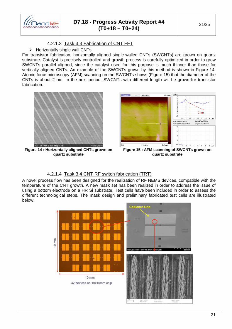
4.2.1.3 Task.3.3 Fabrication of CNT FET Horizontally single wall CNTs
For transistor fabrication, horizontally aligned single-walled CNTs (SWCNTs) are grown on quartz substrate. Catalyst is precisely controlled and growth process is carefully optimized in order to grow SWCNTs parallel aligned, since the catalyst used for this purpose is much thinner than those for vertically aligned CNTs. An example of the SWCNTs grown by this method is shown in Figure 14. Atomic force microscopy (AFM) scanning on the SWCNTs shows (Figure 15) that the diameter of the CNTs is about 2 nm. In the next period, SWCNTs with different length will be grown for transistor fabrication.
Figure 14 : Horizontally aligned CNTs grown on
quartz substrate Figure 15 : AFM scanning of SWCNTs grown on
quartz substrate
4.2.1.4 Task.3.4 CNT RF switch fabrication (TRT) A novel process flow has been designed for the realization of RF NEMS devices, compatible with the temperature of the CNT growth. A new mask set has been realized in order to address the issue of using a bottom electrode on a HR Si substrate. Test cells have been included in order to assess the different technological steps. The mask design and preliminary fabricated test cells are illustrated below.

D7.18 - Progress Activity Report #4 (T0+18 – T0+24)
22/35
22
Figure 16 : Fabrication of CNTs RF switch
4.2.1.5 Task.3.6 CNT based antenna fabrication (TRT/SHT/UPMC) Layout definition for selected antenna integrated technology
Optimized designs on highly resistive Silicon and quartz substrates have been selected and transfered to TRT for process (Figure 17). This final layout allowed the fabrication of sixteen individual CPW CNT-based monopoles, allowing the experimental influence of some keys parameters over measurement results, such as CNT bundle diameter and length, RF access geometry and surrounded ground plane design. Deembedding structures have been also inserted for S-parameter on-wafer calibration standards determination and also for Material parameters extraction (ε, µ).
Figure 17 : Generic layout for CNT-based monopole i n CPW technology (HR Si and quartz substrate)
Technological process issues Following the design, first CNTs antenna has been fabricated. On Figure 18a, we can see the structure realized before CNTs growth. Technological processes matching with expected antenna design have to be overcome, as CNT diameter-to-length ratio is critical (Figure 18b). Some process procedure and design modifications are under work to overcome fabrication constraints.

D7.18 - Progress Activity Report #4 (T0+18 – T0+24)
23/35
23
(a) (b)
Figure 18 : CNTs antenna fabrication and growth
4.2.1.6 Task.3.7 Development of carbon nanotube interconnects (SHT/CHALMERS)
In the past half year, Chalmers have continued to characterize resistance of the CNT interconnects made by the new transfer method. The best single via resistance is around 1.6 Ohm, which is smaller to that of the old method (2.7 Ohm) and the linearity of the I-V curve remains high. This improvement on resistivity is expected, as this new polymer transfer technique is less destructive than the previous indium transfer technique. In the previous process, the CNTs have to be pressed onto the target substrate, which is coated with indium. This pressing process is likely to distort the CNT bundles and introduce bending in the CNT pillars. It is very difficult to avoid such bending as the control of height and pressure during the pressing process is extremely inaccurate, due to the limitation of the flip chip bonder machines. And also, the previous press and heat method requires a third assistant silicon wafer with indium coating serving as the transfer medium for inserting the CNT bundles in to the target silicon wafer. This third substrate is an overburden of the process and thus increases the cost and complexity of the process. On contrast, with our new transfer process, we eliminate the need of the third indium coated substrate, and also the need of compression on the CNT bundles during transfer. This greatly improves the quality of the transferred CNT vias and reduces the complexity, thus cost, of the overall process. The reduced resistance of the CNT vias indicates a good signal that the new method not only improves the yield but also the quality of the CNT vias after fabrication. Chalmers have also managed to stack the CNT TSV interconnect to make multilayer structures. The stacking of two silicon layers with CNT vias is demonstrated. The stacking is achieved by optical alignment and in house isotropic conductive adhesives. After that the whole stacked chip is mounted onto PCB board for testing purpose. The resistance of the stacked CNT vias are measured and compared to the resistance of single layer CNT vias. The average double layer interconnect resistance is around 1.2 Ohm, while the average single layer CNT interconnect resistance is around 0.7 Ohm. The resistance is quite stable across the measurement points of over 8 via interconnects measured for one sample. This result is quite promising as the single layer CNT via resistance is below 1 Ohm, which is suitable for some applications where low resistance requirement is not strict.

D7.18 - Progress Activity Report #4 (T0+18 – T0+24)
24/35
24
4.2.1.7 Task.3.8 Development of RF graphene devices Dielectrics (Tyndall, ICN) The work has continued towards developing a room temperature e-beam process for the growth of high-k metal oxides (HfO2) suitable as gate oxides for graphene (and CNT FET) devices. During reporting period, Tyndall-UCC high-k dielectrics growth activity is summarised as mentioned below:
Two runs of 10nm HfO2 thin films grown by ALD on GaAs substrates with Pd/Au electrodes for FETs on CNT's and on Graphene; these samples have been send to partner FORTH
Three runs of 5, 10 and 15nm HfO2 thin film grown at RT by e-beam on Pt/Ti/Si and on Si substrates • One batch of three samples: 5, 10 and 15nm HfO2 RT beam on Pt/Ti/Si(100) send to
FORTH for conductive AFM/AFM/electrical characterisation; these samples have been send to partner FORTH
• One batch of three samples: 5, 10 and 15nm HfO2 RT beam on Pt/Ti/Si(100) send to IMT for additional characterisation; these samples have been send to partner FORTH and IMT
• One batch of six samples: 5, 10 and 15nm HfO2 RT beam on Si (100), 40nm HfO2 thin film on Si(100), 180 nm HfO2 thin film on Si(100), 420nm HfO2 thin film on Si (111); the samples have been send to partner ICN for XPS, thermal conductivity, AFM measurements
The structural, chemical and thermal properties of high-k metal oxide thin films (HfO2 and ZrO2) were investigated by XPS, AFM, and 3-omega measurements. The samples were grown and provided by Tyndall with varying thicknesses. X-ray photoelectron spectroscopy (XPS) measurements of HfO2 on Si were performed with film thicknesses of 5nm to 420nm. The quantitative analysis of the experimental data provided detailed information of the O/Hf ratio and the binding energies as function of the film thickness for ultra-thin high-k dielectric films. The surface roughness of the HfO2 layers was determined by atomic force microscopy (AFM). All measured samples exhibited a RMS value well below 1nm (0.72nm for 420nm thick HfO2) which represents nearly atomically flat surfaces and demonstrates the well-controlled deposition of the high-k dielectrics by Tyndall. Moreover, the cross-plane thermal conductivity of ZrO2 and HfO2 thin films was measured using the 3-omega method. The thermal conductivity was determined in a wide temperature range between 30 K and 300 K. The cross-plane thermal conductivity at room temperature was found to be 0.88 W/mK for ZrO2 and 0.65 W/mK for HfO2, respectively. Graphene FET (FORTH)
Ohmic contact optimization To improve ohmic contact quality in metal – graphene containing devices, we performed a study of graphene pretreatment before the Pd contact deposition. This resulted in a significant improvement of contact resistance thus reducing the series resistance which is especially important on active devices (FETs). The results are summarized on Table 3

D7.18 - Progress Activity Report #4 (T0+18 – T0+24)
25/35
25
Pretreatment time (sec)
Best measured ρc (specific contact resistivity Ωcm2)
0 3.09e-07
5 1.15e-07
10 4.46e-09
Table 3: Table of specific contact resistivity meas ured on graphene contacts Those results are under investigation regarding the repeatability of the obtained values.
Source – Drain miniaturization Optimizing the source drain distance with respect to the gate length is important to reduce acces resistance and provide an optimum FET device. On Figure 19, we present a 0.2µm wide gate deposited in à.6µm wide source.
Figure 19 : 0.2 µm wide gate deposited in a 0.6 µm wide Source – Drain distance. Note that the sourc e
drain is beyond the specification put forward by th e optical lithography and the resist used. Graphene Antenna (IMT) The fabrication of graphene antenna was presented in the previous report. The fabricated antenna is shown in Figure 20.
D7.18 - Progress Activity Report #4 (T0+18 – T0+24)
26/35
26
Figure 20 : The graphene antenna. A detail of the graphene wafer with few antennas on it is depicted in Figure 21.
Figure 21 : Detail of the graphene CVD wafer with a ntennas on it. The graphene antenna was fabricated on the CVD grown graphene wafer having a substrate doped Si/SiO2. Our intension was to have a good fabrication process and less performance at this level of research, since the CVD graphene wafer on doped Si is not expensive. However, doped Si is a very lossy in microwaves and so the performances of the antenna will be not the best. The technogical process seems to be validated and a second fabrication was carried out on Si HR. From the test structure we have learned that the graphene antenna which must work finally at 10 Ghz need to be two times smaller and to be grown via CVD graphene deposition on a SiO2/high resistivity substrate. Again , the masks and the technological process is depicted below in Figure 22.

D7.18 - Progress Activity Report #4 (T0+18 – T0+24)
27/35
27
Figure 22 : The graphene antenna on high resistivit y Si.
In Fig. 11 different biasing solutions for graphene antenna are proposed.
Figure 23 : Proposed antenna configurations for bia sing the graphene. The role of biasing the graphene is to change the slot properties such that a tunning of S11 to be done. Here the bias the done by polarization of the CPW line and doping the graphene near the two metallic contacts. Also, the same structure will be done on a CVD graphene on a doped SiO2 substrate to test the back gate bias and for performance comparison purposes. First, we have fabricated an antenna at 10 GHz on high resistivity substrate to test its performances. The graphene antenna configuration and some fabricated trsuctures are presented in Fig. 12.
(a) (b)
Figure 24 : Graphene antenna on high resistivity Si .
D7.18 - Progress Activity Report #4 (T0+18 – T0+24)
28/35
28
5 PROGRESS IN THE ACTIVE THECNICAL WORKPACKAGE 4
5.1 WP4 : TEST ACTIVITIES
WP leader Involved Partners
Duration Deliverables Milestones
Active Tasks Status
LAAS
TRT, CHALMERS,
FORTH, LAAS, UPMC,IMT, GI, SHT,UNIVPM, LIU,TYNDALL
T0 +15 – T0+26 D4.1 to D4.7 MS4 T4.1 to T4.6 On Going
5.2 WP OBJECTIVES This work package is dedicated to the electrical characterization (DC to RF) of all the devices fabricated in WP3. The results obtained will be compared with the results obtained through simulations in WP2 and basic equivalent circuit models will be calibrated following parameter extraction from static (DC) to high-frequency (HF) measurements. A strong interaction is planned with WPs 2 and 3, in order to take into account all the fabrication available parameters as well to feedback into fabrication and application design the needed optimization
5.3 PROGRESS TOWARD OBJECTIVES : STATUS OF ACTIVES TASKS
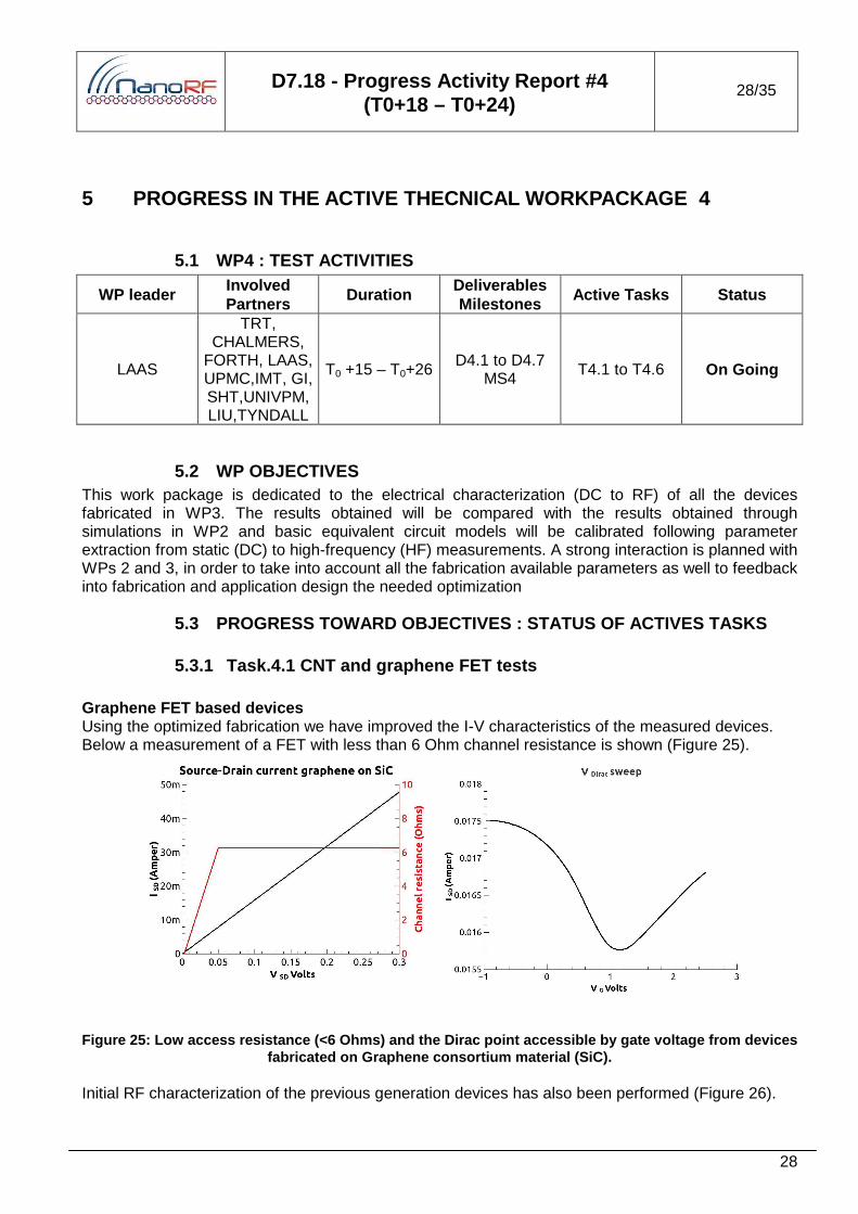
5.3.1 Task.4.1 CNT and graphene FET tests Graphene FET based devices Using the optimized fabrication we have improved the I-V characteristics of the measured devices. Below a measurement of a FET with less than 6 Ohm channel resistance is shown (Figure 25).
Figure 25: Low access resistance (<6 Ohms) and the Dirac point accessible by gate voltage from devices fabricated on Graphene consortium material (SiC).
Initial RF characterization of the previous generation devices has also been performed (Figure 26).

D7.18 - Progress Activity Report #4 (T0+18 – T0+24)
29/35
29
Figure 26 : Previous generation of graphene FET hav e been characterised in RF. Maximum stable gain in embedded data is shown.
CNT FET based devices Carbon nano-tube devices formed out of random nano-tube network have been realised. Those fabrication runs were designed to provide normally off CNT FETs (using a Pd gate).
Initial (first run) fabrication was done with a surface density of 200ngrams/mm2 (Figure 27).
.
Figure 27 : Source – drain current of a CNTFET with 4µm S-D distance and its respective transconductance verifying that that operates as a normally off device
The following runs incorporated smaller S-D distances and are currently under characterization.
5.3.2 Task.4.4 CNT and graphene based antenna tests
CNT antenna on Si
We have measured the S11 of several graphene antennas on the same CVD graphene wafer. The results are depicted in Figure 28 in the UNBIASED CASE. At this level i.e. the test structure the bias was not introduced on the graphene antenna, because we do not have a top electrode for a back-gate configuration.

D7.18 - Progress Activity Report #4 (T0+18 – T0+24)
30/35
30
Figure 28 : S11 for the graphene antenna We see that antenna is resonating arround 5 GHz . The problem of the initial simulations was that it was considered a value of εeff = 2.7, so tha λg = λ0/√εeff = 18.26 mm @ 10 GHz, whereas the effective refraction index n = √εeff = 2.7, hence εeff = 7. From the theory of the slot loop antenna, be 2p the perimeter of the slot, hence we have λg = 2p = 22.4 mm. With the real value of εeff = 7 we have:
• λg = 22.22 mm @ 5 GHz • λg = 11.11 mm @ 10 GHz
This means that the unbiased antenna (the situation considered in the measurements) should resonate around 5 GHz, as it is apparent from the measurements and the simulation in Figure 28. The simulation is close to the measured results, the are some measured values even better for simulations fact that it is typical for antennas since the simulation of free-space in which antenna is working takes a lot of memory and time to simulate it. We note that the peaks of S11 are very wide and this is due to the doped Si substrate which is lossy. Finally, using all the above data, the radiation pattern is depicted in Figure 29.

D7.18 - Progress Activity Report #4 (T0+18 – T0+24)
31/35
31
Figure 29 : The simulated radition pattern.
CNT antenna on Si HR The antennas were fabricated on a high resistivity Si having a thickness of 520 µm and the gold metallization was 0.3 µm. The S11 measured and simulated are presented in Figure 30.
Figure 30 : S11 of the graphene antenna on Si.high resistivity
We see that S11 is within the specs (10 GHz bandwidth , S11 < -10 dB) of the graphene antenna and that simulated results are close to measured results. We see sharp peaks of S11 indicating the strong confinement of the electromagnetic field at the resonance frequency due to absence of strong losses. The radiation was qualitatively measured by pacing above the antenna a receiving antenna –the other probe-tip of the VNA. The results are depicted in Figure 31.

D7.18 - Progress Activity Report #4 (T0+18 – T0+24)
32/35
32
Figure 31 : S21 and gain of graphene antenna on hig h resistivity Si substrate.
We see that antenna radiates maximum where the S11 has a sharp resonance and the expect gain of the antenna is 5 dB at the same resonance frequency of 9.5.Ghz.
6 DISSEMINATION AND EXPLOITATION ACTIVITIES (WP6)
WP leader Involved Partners
Duration Deliverables Milestones
Active Tasks Status
TRT TRT, ICN T0 +0 – T0+36 D6.1 to D6.6 - On Going
6.1 PUBLICATIONS & CONFERENCE A Nano-RF workshop was organized at Rome during the European microwave conference 2014 (06/10/2014)
Publications
• Mircea Dragoman, Detection of electromagnetic waves with a single carbon atom sheet, Proc. Romanian Academy, series A . vol.15, pp.208-215 (2014)
• Martino Aldrigo, Mircea Dragoman,1,and Daniela Dragoman Smart antennas based on graphene, JOURNAL OF APPLIED PHYSICS 116, 114302 (2014)
• Daniela Dragoman and Mircea Dragoman, Enhanced architectures for room-temperature reversible
logic gates in graphene, Applied Physics Letters 105, 113109 (2014)
• Mircea Dragoman, Adrian Dinescu and Daniela Dragoman, Negative differential resistance in graphenebased ballistic field-effect transistor with oblique top gate, Nanotechnology 25 415201 (2014)
• J. S. Reparaz, E. Chavez-Angel, M. R. Wagner, B. Graczykowski, J. Gomis-Bresco, F. Alzina, and C. M.
Sotomayor Torres, "A novel contactless technique for thermal field mapping and thermal conductivity determination: Two-Laser Raman Thermometry", Rev. Sci. Instr. 85, 034901 (2014)

D7.18 - Progress Activity Report #4 (T0+18 – T0+24)
33/35
33
• D. Mencarelli, L. Pierantoni, A. Di Donato, M. Farina, “The close relation between gyrotropic materials and ferrite: application to full-wave solvers”, Journal of Computational Electronics, Dec. 2014
• L. Pierantoni, D. Mencarelli, M. Bozzi, R. Moro, S. Bellucci, “Graphene-based Electronically Tunable Microstrip Attenuator”, Nanomaterials and Nanotechnology, June 2014, 6:14.
• D. Mencarelli, L. Pierantoni, T. Rozzi, F. Coccetti, “Nanoscale Simulation of Three-Contact Graphene Ballistic Junctions”, Nanomaterials and Nanotechnology, April 2014, 4:14, pp. 1-7
• V. Prudkovskiy, "Influence of ozone treatment on the electronic doping of graphene" (poster) Graphene school 2014, Cargese, France, 8-18 April 2014.
• G. Vincenzi, G. Deligeorgis, F. Coccetti, P. Pons, “Open-Thru de-embedding for Graphene RF devices, ” in proceedings of IEEE International Microwave Symposium Tampa 1-6 June 2014.
• G. Vincenzi “Investigation of microwave transport in graphene based devices”, Université de Toulouse –
LAAS-CNRS PhD Thesis Manuscript – Janvier 2014
• Liang Xu, Di Jiang, Yifeng Fu, Stephane Xavier, Shailendra Bansropun, Afshin Ziaei, Shan-Tung Tu, Johan Liu. Effect of substrates and underlayer on CNT synthesis by plasma enhanced CVD, Advances in Manufacturing, 1, 2013.
Conference
• D. Masotti, M. Aldrigo, A. Costanzo, F. Mastri, M. Dragoman, Graphene-Based Nano-Rectenna in the Far Infrared Frequency Band, European Microwave Conference, October 2014, Rome Italy.
• 6M.Aldrigo, M.Dragoman, A. Constanzo, and D. Masotti, Exploitation of Graphene as HIS and RIS for Devices in the MW and THz Frequency Ranges, European Microwave Conference, October 2014, Rome Italy.
• A novel high resolution contactless technique for thermal field mapping and thermal conductivity determination: Two-Laser Raman Thermometry" (oral) E. Chávez-Ángel, F. Alzina, and C. M. Sotomayor Torres, E-MRS spring 2014, 26-30 May 2014, Lille (France)
• "Heat propagation and thermal phonon dynamics in group IV nanostructures" (poster) M. R. Wagner, J. S. Reparaz, J. Gomis-Bresco, E. Chávez-Ángel, B. Graczykowski, F. Alzina, and C. M. Sotomayor Torres, E-MRS spring 2014, 26-30 May 2014, Lille (France)
• "Thermal conductivity and thermal field distribution determination in free-standing Si and Ge membranes" (oral) J. S. Reparaz, E. Chavez-Angel, M. R. Wagner, A. Shchepetov, M. Prunnila, J. Ahopelto, P. Vaccaro, I. Alonso, M. Garriga, A. R. Goñi, F. Alzina, and C. M. Sotomayor Torres, E-MRS spring 2014, 26-30 May 2014, Lille (France)
• "A novel contactless technique for thermal field mapping and thermal conductivity determination: Two-Laser Raman Thermometry" (oral) J. S. Reparaz, E. Chavez-Angel, M. R. Wagner, B. Graczykowski, J. Gomis-Bresco, F. Alzina, and C. M. Sotomayor Torres, NanoSpain 2014, 11-14 March 2014, Madrid (Spain)
• "Acoustic phonon dynamics in free standing group IV semiconductor membranes studied by ultra-fast pump & probe spectroscopy" (poster) M. R. Wagner, J. S. Reparaz, J. Gomis-Bresco, E. Chávez-Ángel, B. Graczykowski, F. Alzina, and C. M. Sotomayor-Torres, NanoSpain 2014, 11-14 March 2014, Madrid (Spain)

D7.18 - Progress Activity Report #4 (T0+18 – T0+24)
34/35
34
• "Impact of boundary scattering on nanoscale thermal transport properties in ultra-thin Si-based nanostructures" (oral) M. R. Wagner, E. Chávez Ángel, J. Gomis Bresco, J. Sebastian Reparaz, A. Shchepetov, M. Prunnila, J. Ahopelto, F. Alzina Sureda, and C. M. Sotomayor Torres, ASME 2013 International Mechanical Engineering, 15-21 Nov. 2013, San Diego (USA)
• "Raman thermometry as contactless method for thermal conductivity determination: The case of thermal conductivity reduction in Si and Ge" (oral) J. S. Reparaz, E. Chávez Ángel, J. Gomis Bresco, M. R. Wagner, J. Cuffe, V. Shah, M. Myronov, D. Leadley, A. Shchepetov, M. Prunnila, J. Ahopelto, F. Alzina Sureda, C. M. Sotomayor Torres, ASME 2013 International Mechanical Engineering, 15-21 Nov. 2013, San Diego (USA)
• "Thermal Conductivity of nm-scale Membranes by Raman Thermometry" (oral) E. Chávez-Ángel, J. S. Reparaz, J. Gomis-Bresco, M. R. Wagner, J. Cuffe, A. Shchepetov, M. Prunnila, J. Ahopelto, F. Alzina, and C. M. Sotomayor Torres, 26th International Microprocesses and Nanotechnology Conference, 5-8 November 2013, Saporo (Japan)
• F. Coccetti, D. Mencarelli, L. Pierantoni, “Carbon Based Ballistic RF Electronics”, Invited Paper, Proc. of Asia-Pacific Microwave Conference 2014, (APMC 2014), Sendai, Japan, Nov. 4-7, 2014.
• L. Pierantoni, D. Mencarelli, M. Bozzi, R, Moro, A. Sindona, L. Spurio, S. Bellucci, “Full-wave techniques for the electromagnetic-quantum transport modeling in nano-devices”, Invited Paper, Proceeding of the 2014 International Semiconductor Conference (CAS 2014), 13-15 Oct. 2014, Sinaia, Romania.
• L. Pierantoni, D. Mencarelli, M. Bozzi, R. Moro, S. Bellucci, “Microwave Applications of Graphene for Tunable Devices”, Proceeding of the 17th European Microwave Week (EuMW), Rome, Italy, Oct. 5-10, 2014.
• L. Pierantoni, D. Mencarelli, “Full-Wave Techniques for the Multiphysics Quantum and Electrodynamics Modeling of Nanodevices”, Invited Paper, Proceedings of the 15th Intern. Conference on Nanoscience & Nanotechnology 2014 (N&N 2014), INFN-LNF, Frascati, Italy, Oct. 6-7, 2014.
• D. Mencarelli, L. Pierantoni, “Modeling and Simulation of Carbon Nanotransistors”, Invited Paper, Proceedings of the 15th Intern. Conference on Nanoscience & Nanotechnology 2014 (N&N 2014), INFN-LNF, Frascati, Italy, Oct. 6-7, 2014.
• L. Pierantoni, D. Mencarelli, Invited Paper, “Numerical simulation of the combined quantum-electromagnetic problem in nano-structured devices”, Proceeding of the 14th IEEE International Conference on Nanotechnology (IEEE-NANO 2014), August 18-21, 2014, Toronto, ON, Canada.
• L. Pierantoni, D. Mencarelli, “Radio-Frequency Nanoelectronics - Bridging the Gap between Nanotechnology and R.F. Engineering Applications”, Proceedings of the 15th annual IEEE Wireless and Microwave Technology Conference (WAMICON 2014), Tampa, Florida, June 6, 2014.
• D. Mencarelli, L. Pierantoni, “Electromagnetic Simulators for the Modelling of Magnetically Biased Graphene”, Proceedings of the 2014 International Microwave Symposium (IMS), Microwave Symposium Digest (MTT), Tampa Bay, FL, USA, June 1-6, 2014, pp. 1-3.
• D. Mencarelli, L. Pierantoni, F. Coccetti, “Nanoscale Modeling of Three-Contacts Graphene Ballistic Junctions: Analysis of the Non-Linear Transport”, Proceedings of the 2014 International Microwave Symposium (IMS), Microwave Symposium Digest (MTT), Tampa Bay, FL, USA, June 1-6, 2014.
• L. Pierantoni, D. Mencarelli, “Advanced techniquse for the electromagnetic-quantum transport modeling in 2D nanomaterials beyond Graphene”, 2014 International Microwave Symposium (IMS). Notes of the Workshop on: Beyond Graphene Electronic Devices and their Potential for High-Frequency Applications”, Tampa Bay, FL, USA, June 1-6, 2014.
• L. Pierantoni, D. Mencarelli, “Efficient Characterization of the Electromagnetic-Quantum Transport Coupling of Wired CNT- and Graphene Antennas”, 8th IEEE European Conference on Antennas and Propagation (EuCAP), The Hague, The Netherlands, 6-11 April 2014.

D7.18 - Progress Activity Report #4 (T0+18 – T0+24)
35/35
35
• RF Nano Electromechanical Systems based on Vertically Aligned Carbon Nanotubes” , Stéphane Xaviera, Yifeng Fub, Johan Liuc, Matthieu Leballifa, Paolo Martinsa, Shailendra Bansropuna, Afshin Ziaeia, Gothenburg, Sweden, European Microwave Conf, Oct -5-10, 2014, Rome, Italy.
• Investigation of the E-beam evaporation and Atomic Layer Deposition of Metal Oxides growth on Pristine Graphene, Mircea Modreanu,Ian Povey, Raluca Gavrila, Mircea Dragoman, Stephane Xavier, Frederic Wyczisk, Andrea Di Donato, Davide Mencarelli, Peter Blake, Yifeng Fu, Johan Liu,George Deligeorgis, EUMW2014