Embed Size (px)
Citation preview

IMT-BucharestIMT-Bucharest
Ministry of Education, Research and Innovation RomaniaMinistry of Education, Research and Innovation Romania
National Authority for Scientific ResearchNational Authority for Scientific Research
Your reliable partner: IMT-BucharestYour reliable partner: IMT-Bucharest
From Technological Services, From Technological Services,
to Scientific Cooperationto Scientific Cooperation

IMTIMT-MINAF-MINAFABAB, launched in Brussels at an event organized by Romania, with the
participation of the European Commission.
On 8th of May 2009, this facility was presented in “New Materials, Micro- and Nanotechnologies: discover a goodpartner in Romania” at Brussells, an event organized by ROST - Romanian Office for Science and Technology fromEuropean Union.
IMT-MINAFAB i.e. “IMT-Centre for MIcro and NAnoFABrication” provides scientific and technological support for partners
from research, education and industry. It is an “open centre”, facilitating easy access in variety of ways.. IMT-MINAFAB
facilitates R&D common projects and the direct access of the innovative companies to technology. Details about MINAFAB
services are available on the web page: http://www.imt.ro/MINAFAB.
Dr. Alexandru Muller, nominated for the
Descartes Prize (2002), is presenting to the
Commissioner the newest results in RF
MEMS obtained with partners which founded
AMICOM (NoE financed by FP 6)
The Commissioner
appreciated IMT as: “... a pioneer of
integration in ERA in Eastern Europe”.
Dr. Renzo Tomellini, Head of Unit
"Value-added materials”, European
Commission, DG RTD,
DG “Industrial Technologies”
Mr. Louis Bellemin,
honorary director of the
European Commission
Prof. Alain Pompidou, President of the
French Academy of Technologies, former
President of the European Patent Office.
Dr. Francisco Ibańez, Deputy Head of Unit
“Micro- and nanosystems ICT Programme”,
European Commission, DG INFSO, DG
“Components & Systems”
Dr. Christophe
Bruynseraede, Business
Program Manager,
IMEC, Belgium
Mrs Mihaela Ionita,
funding coordinator,
INFINEON, Romania
AA visit to remember:visit to remember: MrMr. PHILIPPE BUSQUIN,. PHILIPPE BUSQUIN,the European Commissioner for Research:
IMT as “... a pioneer of integration in ERA in Eastern Europe” (IMT-Bucharest on 6th of February 2004)

Designed by IMT-Bucharest
Your reliable partner: IMT-BucharestYour reliable partner: IMT-Bucharest
From technological services, to scientific cooperationFrom technological services, to scientific cooperation

Your reliable partner: IMT-Bucharest
Table of Contents:
Introduction
IMT in brief
IMT-MINAFAB
Scientific and technological services
� Technological processes
� Mask shop
� Characterization
� Reliability
� Computing
Competences in scientific research
� Microsystems technologies
� Nanotechnology
Education
Technology transfer
Electronic dissemination and networking
Editing and publishing
Organizing scientific conferences and other events

1Your reliable partner: IMT-Bucharest
IMT in briefIMT in brief
The full name of IMT – Bucharest (or simply IMT) is the National Institute for R&D in Microtechnologies
(http://www.imt.ro), a unit coordinated by the National Authority for Scientific Research (Ministry of Education,
Research and Innovation, Romania).
The main competences of IMT are in micro-nanosystems and nanobiotechnology (see the box below). An
interdisciplinary group of laboratories and their top-level equipments is called “Centre of Nanotechnologies”, and
works under the aegis of the Romanian Academy (of Sciences). Another pair of labs - specialized in microwave
and photonics - is grouped as the MIMOMEMS proposal achieved financing by the EC through the REGPOT
programme (2008-2011). IMT became visible at the national level, especially by coordinating various projects
financed from the National Programme MATNANTECH (New Materials, Micro and Nanotechnologies) (2001-
2006). In the period 2003-2009 IMT was involved in approximately 25 European projects (FP6, FP7 and related).
In the landscape of the new member states of UE, IMT is an active actor in RTD. The investments in
equipment (7 millions of euro in 2006-2009) provide an excellent support for the experimental work (details inside
this brochure). Through the Centre for Micro- and Nanofabrication (IMT-MINAFAB) these facilities are
available to customers from industry, research and education (www.imt.ro/MINAFAB).
IMT acts basically as an autonomous, non-profit research company. As far as the participation to national and
European projects is concerned, IMT is assimilated to a public research institution. Apart from scientific research
and technological development, IMT is active in technology transfer and innovation, as well as in education
and training. Since 2005, IMT includes an autonomous Centre for Technology Transfer in Microengineering
(CTT-Baneasa), and in June 2006, a Science and Technology Park for Micro- and Nanotechnologies
(MINATECH-RO) was set-up by a consortium with just two partners: IMT (housing most of the park area), and
University “Politehnica” of Bucharest. The facilities provided to companies in the park include rooms for working
points, priority of access to scientific and technological services provided by IMT, as well as the possibility to
install their own equipments in the technological area of IMT. The last possibility is just to be implemented now
and opens the way for an exchange of services with IMT, including cooperation in a small-scale production. In
2009 IMT put the basis for the cooperation with important international companies.
IMT is open for educational activities in cooperation with universities: undergraduate, M.Sc. and Ph.D. studies,
and also for “hands-on training”. IMT was active in a Marie Curie training by research network and also in
Leonardo programme. Occasional training courses have been provided in IMT by companies and by research
partners in European projects. IMT is organizing the Annual Conference for Semiconductors (CAS), an IEEE
event (CAS 2009 was the 32th edition), now largely devoted to micro- and nanotechnologies. IMT is also
organizing within the Romanian Academy the “National Seminar for Nano-science and Nanotechnologies”
(the 8th edition - in 2009). The institute is editing or co-editing the following publications (all in English): “Micro-and Nanotechnology Bulletin” (quarterly magazine, since 2000); “Romanian Journal for Information Science
and Technology” (since 2008, in the ISI Thomson database), a publication of the Romanian Academy; the series
of volumes “Micro- and Nanoengineering”, in the Publishing House of the Romanian Academy (12 volumes
until 2008).
IntroductionIntroduction
Microsystems technologies are the core of technologies of the IMT Bucharest. Based on these technologies many
innovative devices are designed, characterized and fabricated. These devices divided in three main categories:
(i) RF MEMS (RF MicroElectroMechanicalSystems) which address the applications of microsystem technologies in the area
of microwaves and millimeter waves with applications in advanced communications systems
(ii) Optoelectronics and photonics which are dealing with the microsystem technologies at optical wavelengths based on
the key concept of MOEMS (MicroOptoElectroMechanicalSystems) The RF MEMS and MOEMES devices are the key
concept of the European Center of Excellence MIMOMES financed by UE unifying research forces and equipments in these
groundbreaking microsystems technologies covering the electromagnetic spectrum from RF up to infrared wavelengths.
(iii) Sensors are key components focussed for a better quality of live of the citizens. Based on the microsystems
technologies sensors are the key devices to detect pesticides or herbicides in water or in the food, toxic gases, or to provide
an early warning alarm in construction or bridges, or cancer or other harmful illnesses. Microsystems technologies allow
the miniaturization of the sensors such that they are integrated in walls, in paper, or other materials conferring them a sort
of “intelligence”. We are developing smart walls, smart paper and smart dust. The sensor activities are merged in a Center
of Research for the Technologies Integration.

2 Your reliable partner: IMT-Bucharest
“IMT“IMT-MINAF-MINAFAB” IMT Centre for MIcro and NAnoFAB” IMT Centre for MIcro and NAnoFABricationABrication
A new infrastructure initiated in 2008, IMT-MINAFAB, should be seen as an interface which will be created byIMT-Bucharest in order to fully exploit its tangible and intangible assets in micro- and nanotechnologies(clean-room facility, equipments, human resources, partners and clients). The so-called “fabrication
centre” will be in fact a complex technological platform including also CAD tools, characterization
equipments, a mask shop, a reliability lab. The fabrication itself, whenever necessary, is accompanied by
specific testing and design, as shown in the following examples:
(i) the COVENTOR software package for modelling and simulation of microsystems provides design verification,as well as the direct input data for mask fabrication; (ii) the on-wafer RF testing allows immediate testing of experimental RF components; (iii) the nano-plotter and microarray scanner (NanoBioLab, in cleanroom environment) allow on-chip controlleddeposition of biological molecules etc.The term “fabrication” in this context means “physical realization” and not necessarily production. In some
cases, the equipments can be used for both research and “small-scale production”.
The role of IMT's R&D laboratories in MINAFAB is twofold. First, they operate the characterization and design
tools, and secondly, they provide multivalent research expertise, from quantum dots to microarrays and from
novel CNT applications to micro- and nanofluidics. The majority of the equipments were purchased through the
investments taking place recently (approximativelly 6.5 million euro in 2006-2008).
Clean room facilities, class 1,000 (200 sqm). The present clean room (class 100 to class 1000) contains a mask
shop with a DWL 66 (1 mm resolution), RIE, vacuum deposition system (E-Beam and sputtering), double-face
alignment, deep pen nanolithography, etc. A new clean room (to be operational in 2009) will contain LPCVD,PECVD, APCVD, RTP equipments, etc.). Characterization area, class 100,000 (220 sqm): The
characterization area (class 100,000) is equipped with SEM/EBL, nanoengineering workstation (Raith
e_Line), FEG-SEM, SPM (AFM, STM etc.), nanoindenter, X-ray difractometer, Raman Spectrometer, SNOM,
WLI, electrochemical impedance spectrometer, fluorescence, phosphorescence and lifetime
spectrometer, nanoplotter and nanoscanner for microarrays, etc.
A strategic target for IMT-MINAFAB is to initiate at the national level a network of complementary facilities in
micro- and nanotechnologies. Such a network is planned to be set-up in 2009 starting from the links established
between IMT and other RTD institutes in the so-called “technological networks” (financed between 2005 and
2008), as well as in common research projects. IMT intends to exchange services with such partners and mostly
elaborate a joint offer of services to third parties. Partnerships with external organizations are also extremely
important. Existing partners are LAAS/CNRS, Toulouse, France, and FORTH, Heraklion, Greece, the interaction
being financed by twinning activities within the MIMOMEMS centre of excellence.
As far as the industrial clients are concerned, IMT is promoting cooperation in two ways: first, usingMINATECH-RO, the science and technology park for micro- and nanotechnologies (whereby, for example,companies can place their own equipment in the technological area); secondly, by facilitating the interaction withother companies and research groups through the network for knowledge and technology transfer with more than60 partners (the information is exchanged through the Centre for technology transfer in micro-engineering, partof IMT). Partnership with important foreign companies should be promoted, whenever possible.
The basic categories of services are: • Partnership in RTD activities, sharing the IP resulting from common
research (with research centres, universities, companies); • Scientific and technological services, including
design, consultancy, training and education (for universities and companies); • Direct access to equipments for
“hands-on” activities, after appropriate training (for companies protecting their IP, for postgraduate and
postdoctoral students).
How to access IMT-MINAFAB?• First, consult the extended information about the equipments and technologies available on the public website
at: http://www.imt.ro/MINAFAB. You may also e-mail a request for further details to the person in charge with
certain equipment (the process engineer or the application scientist).
• If you are ready to order a service, please contact the IMT-MINAFAB executive team, by emailing at:
[email protected]. Inquires could be also made by fax at +40-21 490 82 38 or by phone at +40-21 490 82 12 ext
19 (Dr. Radu Popa).

Scientific and technological servicesScientific and technological services
Your reliable partner: IMT-Bucharest
�� Mask manufacturing using Pattern generator - DWL 66fs Laser LithographySystem
• Applications: It can be used for mask
manufacturing or direct exposure on basically
any flat material coated with photoresist.
Numerous optional features increase the
flexibility and make the system suitable for more
applications. If one of your applications requires
a special technology, it can most likely be
implemented in the DWL 66FS.
• Critical Dimensions Specifications: The
current spec for the critical dimensions is 2
micron with a 0.2 micron tolerance. The CD can
be pushed down to 2 micron, but results depend
strongly on the layout and are not guaranteed.
• Mask File Acceptable Formats: Either CIF of
GDSII formats are preferred. DXF is also acceptable, but please verify the pattern with the process engineer
before submitting it as we have found incompatibility problems.
• Available Plates: We currently have Chrome Soda Lime Masks and the available sizes are 4inch, 5inch, and
6inch (maximum 6 inch, only on command). We DO NOT supply Iron Oxide masks and there is currently no plan
to have that kind of masks available in the near future. If you need Iron Oxide, please contact other mask shops.
• Cost of Mask: to estimate the cost of the mask, the extents of the pattern have to be specified. The extents
are the X and Y dimensions of a rectangle that completely covers all the features of the pattern of the mask. Once
you have these dimensions, you can contact the process engineer to obtain the cost of the mask.
• Mask fabrication time: depends on the masks design and the number of masks requested. An average time
of about 2 day after the file is accepted, for dimensions bigger than 5 microns and for dimensions between 1-4
microns it strongly depends of the area to expose and it can be about 6 days.
If you want to order a mask please visit www.imt.ro/MINAFAB/ or contact:
Eng. Gabriela Dragan, ([email protected]); Eng. Florentina Gheorghe, ([email protected])
�� Double Side Mask Aligner - MA6/BA 6 (Suss MicroTec)
Description
• 4”,5”, fragments >5x5 cm;
• Alignement range: X: ± 10 mm; Y: ± 5 mm ; Θ: ± 5ο.
Mechanical increment resolution: 0.1 µm.
• Top side alignment (TSA)–optical microscope “split field”, 0.5
µm.
• Bottom side alignment – high resolution LCD cameras, 0.1 µm.
• Enhanced Image Storage System (EISS).
• Exposure: contact, vacuum, proximity, flood.
• UV 365 nm, 1000 W (Hg).
• DEEP UV 249 nm 500 W (Hg / Xe).
• UV- NIL
Applications:
All standard litography; double side alignment/exposure ()UV,
DUV); nanoimprint litography (NIL) for 4’’-6’’.
Contact person: Eng. Adrian Albu, [email protected]
3
1. PROCESSING SER1. PROCESSING SERVICESVICES

4
Scientific and technological servicesScientific and technological services
Your reliable partner: IMT-Bucharest
�� Structuring at nanoscale range using Electron Beam Lithography andnanoengineering workstation- Raith e_Line from RAITH GmbH
Ultra high resolution EBL (Electron Beam Lithography)
and nano engineering workstation Raith e_Line is a
versatile electron beam lithography system having
complied with the specific requirements of
interdisciplinary research, which allow nanoscale
structuring. Selected options for nanomanipulation,
EBID and EBIE expand this system to a nano-
engineering workstation.
Basic hardware features:
• Thermal assisted field emission gun;
• Minimum line width < 20 nm; Stitching accuracy 40
nm; Overlay accuracy 40 nm; • Cross-over free column with highest beam current density at 2 nm spot size; •
Laser interferometer stage with 100 mm by 100 mm travel range and 2 nm resolution achieved by closed-loop
piezo-positioning; • 10 MHZ DSP-controlled digital pattern generator; • Optional gas injection system up to five
capillaries, nanomanipulators, optical microscope, loadlock, FBMS mode exposure;
Applications: The state-of-the-art e_LiNE electron column matches perfectly with a number of key applications
in: nanoelectroniccs, photonic crystals (PCs), Difractve Optic Elements (DOE), CNTs interconnects,
nanodevices and nanosystems for fundamental research and bio applications. • Nano lithography with sub 20 nm
resolution; • High speed devices e.g. HEMT; • CMOS process and device developments; • Resist-less
lithography; • E-beam induced deposition and etching (EBID-EBIE); • Imprint template fabrication; • Nano probing
and electrical measurements; • Nano and pattern placement metrology; • Gratings, DFB lasers, SAW devices;
Partnership: • CATHERINE - Carbon nAnotube Technology for High-speed nExt-geneRation nano-InterconNEcts, STREP, FP7-ICT, 2008-2011.Project Coordinator: Consorzio Sapienza Innovazione (CSI).
web: http://www.catherineproject.eu/
Contact person: Phys. Adrian Dinescu, [email protected]
SAW device for microwave applications obtained using EBL lithography (details of digits
and interdigits 150 nm)
Mix-and-match lithography for biomedical applications: optical lithography (left),
combined with EBL (right)
High aspect ratio (12:1) structures
in PMMA with applications in
nanotechnology. top: crosslines;
bottom nanopilars.

Scientific and technological servicesScientific and technological services
Your reliable partner: IMT-Bucharest
�� Dry etching processes using Reactive Ion Etching (RIE) Plasma Etcher-Etchlab 200 (SENTECH Instruments, Germany);
Reactive Ion Etching instrument, manual loading, capable of processing wafers up to 6", four process gases:
CF4, SF6, O2 and Ar, maximum RF power 600W, equipped with a fore pump and a turbo molecular pump
capable of reaching pressures in the reaction chamber down to 10-6 mbar.
Applications:
• the etching of dielectrics (SiO2, Si3N4),
• semiconductors (Si),
• polymers and metals (Au, Pt, Ti, Ni).
Contact person: Dr. Marioara Avram ([email protected])
�� Chemical deposition processes
• PECVD - LPX-CVD, with LDS module (STS, UK);
• LPCVD - LC100 (AnnealSys, France);
• APCVD - PYROX (Tempress, UK);
�� Physical deposition using Electron Beam Evaporation an DC sputteringsystem - AUTO 500 (BOC Edwards, UK);
Front loading thin film system for R&D or pre-production services (500mm
x 500mm chamber). Flexible substrate dimensions: 260mm-diameter
work-holder plate. Up to 6 coatings in a single vacuum process (4 E-Beam,
and 2 DC-sputtering). Coating materials using sputtering system: Al, Cr,
Au AlSi1%,ITO,Si,Nb,Ti . Up to 250oC substrate heating. Optional
substrate plasma pre-cleaning. Ultimate vacuum: 7 x 10⁻⁷ mbar. PLC
control and thickness monitoring with 0.1 nm resolution.
Applications: Vacuum depositions of thin films of Al, Cr, Au,Ti electron-
beam evaporation.
Contact person: Eng. Carmen Iorga, [email protected]
�� Nanoprint (also rapid prototyping regim) using Dip Pen nanolithography System
It allows the drawing of dots and lines with sizes as small as 20 nm under
controlled conditions. Complex figures may also be realized. Is a
nanolithography system that "prints" an "ink" directly on the substrate. The
size of the geometrical features can vary from few tens of nanometers (in
best conditions - 20 nm) up to several microns. It allows both a bottom-up
approach and a top-down one when constructing the nanostructures. The
working principle is that of wetting an AFM-type cantilever with an "ink"
and writing down onto a substrate, similar with an ink pen that writes on a
paper. The process is serial and is quite slow, but can be highly
parallelized by using 2D arrays of cantilevers (55,000 such cantilevers on
an array) and thus becomes efficient from the speed and through output
points of view. Many materials can be used as "inks", as are solutions of polymers, small organic molecules, sol-
gel precursors, macromolecules, nanoparticle colloids.
Applications: • surface functionalization (with direct liaison to proteomics, DNA recognition, virus identification);
• photolithographic masks correction; • molecular electronics; • realization of master stamps for NIL (Nanoimprint
lithography); • novel devices (photonic and electronic);
Contact Person: Dr. Phys. Gabriel Moagar-Poladian, [email protected]
5

6
Scientific and technological servicesScientific and technological services
Your reliable partner: IMT-Bucharest
2. MICROPHYSICAL2. MICROPHYSICAL CHARACTERIZACHARACTERIZATION TION
�� Scanning Electron Microscopy characterization of materials and devicesusing Field Emission Gun Scanning Electron Microscope (FEG-SEM) - NovaNanoSEM 630 (FEI Company, USA)
The equipment is a high-quality nanoscale research tool that offers a
variety of applications that involve sample characterization,
analysis and prototyping. It features a superior low voltage
resolution and high surface sensitivity imaging in the range of Ultra
high Resolution Field Emission Scanning Electron Microscopes (UhR
FE-SEM). The Nova NanoSEM 630 presents also low-vacuum
imaging capabilities for spectacular nanoscale characterization on
charging and/or contaminating nanotech materials. The
NovaNanoSEM 630 also offers the most extensive set of tools for
nanoprototyping, including an on-board digital pattern generator and
dedicated patterning software, a high speed electrostatic beam
blanker, gas injection system for direct electron beam writing of
nanostructures and its high stability 150 mm piezo stage.
Basic hardware features:
• Ultra-high resolution characterization at high
and low voltage in high vacuum: 1.6 nm @ 1
kV;
• Beam deceleration mode with sub-100 V and
high surface sensitivity imaging;
• Low and very low kV backscattered electron
imaging for compositional characterization in
high and low vacuum;
• Novel high stability Schottky field emission
gun enabling a beam current up to 100 nA for
analysis;
• 150 x 150 mm high precision and stability
piezo stage;
• True high resolution low vacuum FESEM, with
a resolution of 1.8 nm @ 3 kV;
• The characterization solution for charging
and/or contaminating nano-materials/devices;
• Full prototyping solution with on-board 4 k x 4
k digital pattern generator, dedicated patterning
software, fast beam blanker and gas
chemistries;
Applications: microphysical characterization
of a variety of challenging nanotechnology
materials such as metals, magnetic materials,
nano-particles and powders, nano-tubes and -wires, porous materials (e.g. silicon), plastic Electronics, glass
substrates, organic materials, diamond films, cross-sections, microdevices etc.
Targeting: • RESEARCH: Materials Qualification; Materials&Sample Preparation; Nanoprototyping;
Nanometrology; Device Testing and Characterization;
• INDUSTRY: Macro Sample to Nanometer Metrology; Particle Detection and Characterization;
Partneship: CATHERINE- Carbon nAnotube Technology for High-speed nExt-geneRation nano-InterconNEcts,
STREP, FP7-ICT, 2008-2011, Project Coordinator: Consorzio Sapienza Innovazione (CSI).
web: http://www.catherineproject.eu
Contact Person: Phys. Adrian Dinescu, [email protected]
The structure of an composite
material used in aeronautics-
sample from INFN Italy
Detail of a SAW structure
patterned with e-beam lithography
Micro and nanospheres produced
in the process of CNTs growth.
Porous alumina membrane
covered with Ni catalyst used as
template for CNTs growth
Scientific and technological servicesScientific and technological services
Your reliable partner: IMT-Bucharest
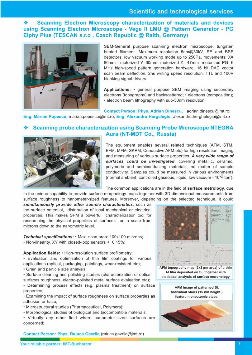
�� Scanning Electron Microscopy characterization of materials and devicesusing Scanning Electron Microscope - Vega II LMU @ Pattern Generator - PGElphy Plus (TESCAN s.r.o , Czech Republic @ Raith, Germany)
SEM-General purpose scanning electron microscope, tungsten
heated filament. Maximum resolution 5nm@30kV, SE and BSE
detectors, low vacuum working mode up to 250Pa, movements: X=
80mm - motorized Y=60mm -motorized Z= 47mm -motorized PG- 6
MHz high-speed pattern generation hardware, 16 bit DAC vector
scan beam deflection, 2ns writing speed resolution, TTL and 100V
blanking signal drivers.
Applications: • general purpose SEM imaging using secondary
electrons (topography) and backscattered; • electrons (composition);
• electron beam lithography with sub-50nm resolution;
Contact Person: Phys. Adrian Dinescu, [email protected];
Eng. Marian Popescu, [email protected]; Eng. Alexandru Hergelegiu, [email protected]
�� Scanning probe characterization using Scanning Probe Microscope NTEGRAAura (NT-MDT Co., Russia)
The equipment enables several related techniques (AFM, STM,
EFM, MFM, SKPM, Conductive AFM etc) for high resolution imaging
and measuring of various surface properties. A very wide range ofsurfaces could be investigated, covering metallic, ceramic,
polymeric and semiconducting materials, no matter of sample
conductivity. Samples could be measured in various environments
(normal ambient, controlled gaseous, liquid, low vacuum - 10-2 torr).
The common applications are in the field of surface metrology, due
to the unique capability to provide surface morphology maps together with 3D dimensional measurements from
surface roughness to nanometer-sized features. Moreover, depending on the selected technique, it could
simultaneously provide other sample characteristics, such as
the surface potential, distribution of local mechanical or electrical
properties. This makes SPM a powerful characterization tool for
researching the physical properties of surfaces on a scale from
microns down to the nanometric level.
Technical specifications: • Max. scan area: 100x100 microns;
• Non-linearity, XY with closed-loop sensors < 0.15%;
Application fields: • High-resolution surface profilometry;
• Evaluation and optimization of thin film coatings for various
applications (optical, packaging, paintings, wear-resistant etc);
• Grain and particle size analysis;
• Surface cleaning and polishing studies (characterization of optical
surfaces roughness, electro-polished metal surface evaluation etc);
• Determining process effects (e.g. plasma treatment) on surface
properties;
• Examining the impact of surface roughness on surface properties as
adhesion or haze;
• Microstructural studies (Pharmaceutical, Polymers);
• Morphological studies of biological and biocompatible materials;
• Virtually any other field where nanometer-sized surfaces are
concerned;
Contact Person: Phys. Raluca Gavrila ([email protected])
AFM topography map (2x2 μμm area) of a thin
Al film deposited on Si, together with
statistical analysis of surface morphology
AFM image of patterned Si.
Individual stairs (15 nm height )
feature monoatomic steps.
7

Scientific and technological servicesScientific and technological services
Your reliable partner: IMT-Bucharest
�� Nanomechanical characterization using Nano Indenter G200 -Nanomechanical Characterization Equipment Agilent Technologies
G200 is a nanomechanical characterization equipment which provides access
to various mechanical properties of small-volume samples, such as thin
films, but could be equally applied to investigate bulk samples. The Nano
Indenter G200 enables users to measure Young's modulus and hardness in
compliance with ISO 14577 and ASTM 2546 standards. The patented CSM
technique yields the elastic modulus and hardness values as a function
of depth in a single measurement (especially useful for thin films) and
allows characterization of the time dependent mechanical behavior of
samples (e.g. polymers).
Applications: High resolution mechanical characterization of a wide
variety of materials (metals, semiconductors, ceramics, biocompatible
materials), especially in the form of thin films, coatings etc. The
characterized properties include hardness, Young’s modulus, film
adherence, wear behaviour, dynamic testing of polymers.
Contact Person: phys. Raluca Gavrila, [email protected]
�� Microphysical characterization using Scanning Near-field OpticalMicroscope - SNOM (Witec alpha 300S, Witec, Germany)
The Alpha300S System is a Scanning Near-field Optical Microscope that
combines the characterization methods of SNOM, Confocal Microscopy
(CM) and Atomic Force Microscopy (AFM) in a single equipment. The
Alpha300S uses patented micro-fabricated SNOM cantilever sensors
(aperture size typically 100nm) for optical microscopy with spatial
resolution below the diffraction limit (optical resolution of 50-100 nm).
Operating modes: Near field optical microscopy: transmission,
reflection, collection, fluorescence; Confocal microscopy: transmission,
reflection, fluorescence, can be upgraded with a Raman spectrometer; Atomic force microscopy: contact and AC–
Mode. The flexibility of this equipment and its operation modes allows a large variety of applications innanotechnology and nanosciences. It allows the optical characterization (in transmission and reflection mode) of
various samples (nanostructures, biological samples, polymers) with a resolution of 50-90 nm in visible spectral
range with the possibility of extension in the IR range. Working in the collection or photon
scanning tunnelling microscope (PSTM) mode the SNOM allows the imaging of
propagating optical field in various metallic and dielectric waveguides providing a powerful
method to characterize and investigate nanophotonics and nanoplasmonic structures and
devices. The AFM module working in both contact and alternative contact modes (with
possibility of extension to magnetic force measurements and pulsed force mode) allows
the topographical and chemical characterization of various surfaces and nanostructures.
Applications: Imaging the optical properties of a sample with resolution below the
diffraction limit with applications in nanotechnology, nanophotonics, nanooptics and
plasmonics; Materials research and polymers; Single molecule detection; Life sciences;
Partnership: • MIMOMEMS - European Centre of Excellence in Microwave, Millimetre
Wave and Optical Devices, based on Micro-Electro-Mechanical Systems for Advanced
Communication Systems and Sensors (FP7-Capacities) 2008-2010; Coordinator: IMT-Bucharest. web: http://www.imt.ro/mimomems/
• FLEXPAET - Flexible Patterning of Complex Micro Optical Structures using Adaptive
Embossing Technology (IP- FP7/NMP) 2008-2010; Coordinator: Fraunhofer Gesellschaftzur Förderung der angewandten Forschung e.V. Fraunhofer Institut fürProduktionstechnolgie (IPT). web: http://www.e-squizoide.com/flexpaet/project.php
Contact Person: Dr. Cristian Kusko ([email protected])
Nanostructure
characterized on SNOM:
top - transmission mode
image of a hexagonal
array of Al regions
deposited on a glass
substrate (Fisher pattern).
bottom - reflection mode
image of an array of
polymer stripes realized
by EBL.
Depth profiling of Young’s modulus
for a thin SiO2 film grown on Si
8

Scientific and technological servicesScientific and technological services
Your reliable partner: IMT-Bucharest
�� Investigations of electrochemical active surfaces using Scanning Electro-chemical Microscope - ElProScan (HEKA, Germany)
The HEKA ElProScan is an Electrochemical Probe Scanner used to characterize processes and structural
features of the samples. The scanning electrochemical microscopy (SECM) resembles the scanning tunneling
microscopy (STM) technique in its use of a tip to scan over a substrate surface, the fundamental difference in
principles of operation being determined by the nature of recorded currents: in SECM the current is carried by
redox processes at tip and substrate in solutions.
System components:
• Bipotentiostat/Galvanostat PG340 with two low current
Preamplifiers.
• High precision real time controlled positioning system with
3 stepper motors mounted on a stable holder made of
granite and a piezo translator; resolution in XY: 100 nm or 15
nm stepper motors, resolution in Z: 100 nm stepper motor +
Fast real time controlled Z-piezo with 5 nm resolution and
100 mm scan range, closed loop regulated.
• Real-Time Computer System with real-time processing
boards, counter and data acquisition modules - software
POTMASTER with SCAN extension.
Applications:
• Surface science: SECM is not only able to reveal the topography (3D images) of samples in solution, but it
may also detect and visualise local variations in the conductivity and electro-chemical reactivity of the
investigated samples. For example, measuring the catalytic activity of microelectrode arrays directly and local
distribution of feedback currents allows a quality control of microsensor production.
• Two dimensional mapping of reaction rates: spatially resolved imaging of dc and ac transport properties by
nanoimpedance spectroscopy (NIS) technique allows the correlation of average transport properties with
individual microstructural elements. Therefore, Nanoimpedance Microscopy/Spectroscopy (NIM) has both
imaging and spectroscopic modes that differentiate processes at interfaces and defects by the time constants
associated with local relaxations.
• Bioelectroanalysis: SECM is a powerful approach for imaging chemical gradients in the diffusion layer
surrounding cell and tissue, the catalytic activity of immobilised enzymes/antibodies, or hybridisation events on
DNA microarrays.
• Characterization of hybrid interfaces and interfacial processes with high spatial and temporal resolution,
including: study of charge transport at the interface between two immiscible electrolyte solutions (ITIES),
molecular transport across membranes, heterogeneous electron-transfer reactions, adsorption/desorption
processes, corrosion processes. For example, polyelectrolyte, electronically conductive polymers, passivation
films on metals and dissolution processes.
• Micropatterning: is a convenient tool for local surface derivatization due to its ability to generate micrometric
sources of a broad range of reactive chemical species. By means of SECM, it is possible to induce a local
polymerisation process under the positioned micro-electrode resulting in a well-defined functionalised polymer
spot at which enzymes, e.g. glucose oxidize, could be covalently immobilized and moreover the surfaces can
also be local structured with different thiol monolayer by means of micro-contact printing with high reproducibility.
Contact Person: Dr. Mihaela Miu, [email protected]
9

Scientific and technological servicesScientific and technological services
Your reliable partner: IMT-Bucharest
�� X-ray Metrology in Semiconductor Industry using Ultra High TrIple AxisRotating Anode 9kW X-ray Thin Film Diffraction System, Rigaku SmartLab,(Rigaku Corporation, Japan)
Main technical characteristics are:
• 9kW rotating anode (45kV, 200mA), up 200mm wafer samples, triple
axis, vertical goniometer, independent theta - theta arms, horizontal
sample mount, Euler cradle (chi, phi, omega independent axis), in-
plane arm, DTexUltra 1D high speed real time detector (SSD–Silicon
multistrip);
• Automatic software alignment (or manual user computer controlled
alignement) of the optics modules and sample for each measurement;
• Bragg-Brentano (+1D DTexUltra SSD detector), parallel beam
(multilayer mirror), different monochromators/analyzers (Ge(220)
crystals with two and four bounce reflections, Ge(440) four bounce
reflection, graphite C(0002) analyzer bent/flat,etc.), X-Y micro area
mapping unit-phase composition, strain&stress, tilt&twist, lattice
parameter modifications/values Δd/d=10-7–10-9, depth distributions of
phase composition, strain, etc;
SmartLab makes thin films analysis more flexible. SmartLab approach is to aid users in choosing the specific
measurement conditions, experimental geometries and application methods best suited to their particular
sample. The system is multimodular (quick alignment computer aided, small measurement time), X-ray sources
9kW rotating anode, real time ultraspeed detectors and diffraction data processing (software, databases, etc).
The system offers multiple measurement techniques:
• X-ray Powder Diffraction (XRPD), can use DTexUltra high speed
SSD;
• High resolution Powder Diffraction (polycrystals) - HRXRPD,
using expanded range of monochromators: Ge (220) 2/4 bounce
Ge(440) 4 bounce and the and the new CALSA analyzer - Ge(111)
high performance compact multi-crystal single reflexion analyzer;
• High resolution X-ray diffraction (HRXRD) (including multiple
reflection HR-MRMCXRD Ge(220) 2/4 bounce monochromator,
Ge(440) 4 bounce monochromator, Ge(220) 2 bounce analyzer,
focussing/flat diffracted beam monchromator);
• X-ray reflectometry (XRR, including HRMR XRR);
• Grazing incidence diffraction (GIXRD);
• Transmision diffraction&SAXS measurements;
• In-plane grazing incidence diffraction (IPGID);
• Small angle X-ray scattering (SAXS, USAXS);
• Single crystal diffraction (SCD);
Some of the characterized structure parameters are:
• multilayer structure&thickness&composition (1~103nm), density
(H2O~Heavy metals), roughness (0.2~several nm);
• phase identification- interface, transition layer;
• crystal structure-crystal quality, lattice parameter (several nm);
• crystal orientation-single: orientation relation of the substrate and
film;
• poly: preferred orientation, pole figures; particle/pore size analysis
1~102 nm;
Applications: • crystal structure (HR RSM, HR RC); • film thickness, density, roughness; • characterization of
the ultra thin film (in plane XRD, grazing incidence); • particle/ pore size analysis (reflection SAXS, transmission
SAXS); • phase identification, crystal structure (powder/thin film/poly/ mono/ crystal, trace, small area/quantity);
Persoana de contact: Phys. Mihai Danila, [email protected];
RSM [parallel beam+Ge(220)4 bounce
monochromator of 300nm(400)-
InP/p+InGaAs(1mm)/n-InP(2mm)/n+-InP,
symetric reflection
High resolution (Ge (220) 4 bounce mono) and
ultra high resolution X-ray diffraction spectra
(Ge(220) 4 bounce mono and Ge (220) 2
bounce analyzer
10

Scientific and technological servicesScientific and technological services
Your reliable partner: IMT-Bucharest
�� Non-contact profiling surface measurements by interferometry using WhiteLight Interferometer - Photomap 3D (Fogale Nanotech, France)
The white light interferometer perform optical, non-contact profiling of rough surfaces, that uses
interferometric techniques as well as digital signal processing algorithms to produce fast, accurate,
repeatable two and three-dimensional surface profile
measurements. The method of determining surface height is based on
white light as the source in an interferometer, and measurements of the
fringe modulation degree, or coherence, instead of the phase of
interference fringes. The white light interferometric profilometer uses the
measurement of surface height through vertical scanning of the reference
arm of the interferometer, and calculate the relative modulation of the
intensity signal as a function of vertical position. The equipment present
sub-nanometer vertical resolution (down to 0.1 nm), non-contact
measurements allowing accurate and repeatable results, all axes
motorization enabling automatic stitching of multiples fields of view, sub-
nanometric roughness measurements, reflectivity 1% to 100%, ability to
measure transparent films and require no sample preparation.
Characteristics: • manual translation stage 100x100 mm range, 20µm resolution; • optical head vertical range
150mm; nanometric objective translation unit; capacitive sensor closed loop control, 500µm range; • white light
and Monochromatic light source; • automatic switching, software control; antivibration feet; • field of view 126x96
µm up to 2.5x1.9mm depending on objective (without zoom); • white light profilometry, 3nm rms z resolution;
• monochromatic light profilometry, 0.1nm rms z resolution; • automatic step height and roughness measurement;
• semi-automatic focus detection; • results exploitation (heights, roughness, dimensions, field stitching, filtering,
3D view, bump size, height, roughness measurements); • motorized x0.35 to 1.6 zoom; • out of plane
measurements (by stroboscopic interferometry within range 100Hz-2MHz and by time averaged operation
without frequency limitations); synthesized function generator: 2 channels controlled by software (one channel
for stroboscopic illumination, the other one for MEMS AC voltage supply); • high voltage module (amplitude up
to 200V; offset up to 200V; 1% resolution; sinusoidal and square signal; power 20W; current output max 100mA);
• multi-reflectivity (5%,25%,50%,85%) objectives (x2.5, x5, x20); • motorised XY stage; • active vibration isolation
stage.
Applications: • surface topography of diverse materials (metals, plastics,
semiconductors, biological materials etc); • residual stress measurement
for different thin film deposition layers; • conceived not only for statistical
surface roughness measurements but also for high precision
measurement of mechanical or chemical micromachining;
• transparent layers thickness measurements (plastics, glasses or
varnish) with known refraction index; • MEMS dynamic measurements
Partnership: • MEMS-4-MMIC- Enabling MEMS-MMIC technology for
cost-effective multifunctional RF system integration; STREP, FP7-ICT-
2007-2, Contract no. 204101, 2008-2011; Coordinator: IMST GmbH. web:
http://www.mems4mmic.com/
• MIMOMEMS-European Centre of Excellence in Microwave, Millimetre
Wave and Optical Devices, based on Micro-Electro-Mechanical Systems
for Advanced Communication Systems and Sensors, FP7-Capacities,
2008-2010; http://www.imt.ro/mimomems
• GIGASABAR-SAW and FBAR type resonators dedicated to
applications in communications for 2-6 GHz, based on micro and
nanomachining of wide band semiconductors (GaN and AlN); PN II
Partnership, 2008-2011; http://www.imt.ro/gigasabar
• MIMFOMEMS - Advanced circuits for microwave, millimeter wave and
photonics based on MEMS technologies, PN II Partnership, 2007-2010,
http://www.imt.ro/mimfomems
Contact Person: Dr. Alina Cismaru, [email protected]
Optoelectronics: SU8 guide
manufactured on silicon substrate
Analysis of the stress influence
over the circuit topography
11

Scientific and technological servicesScientific and technological services
Your reliable partner: IMT-Bucharest
�� Spectroscopy services using High Resolution Raman Spectrometer -LabRAM HR 800 (HORIBA Jobin Yvon, Japan)
LabRAM HR 800 Raman Spectrometer is a powerful optical technique for
materials study and characterization based on inelastic scattering of light
due to light-matter interaction during which the wavelength of the incident
laser will be shifted. This energy loss is characteristic for a particular bond in
the molecule. The Raman spectrum provide qualitative and quantitative
information: peak position is determined by chemical species; line intensity
is proportional to concentration; shift in position of the peak indicate the
stress and temperature effect and the line width the structural disorder.
Characteristics: • Flexible system with confocal microscope and mapping
options; • He-Ne laser (λ = 633 nm) and tunable air cooled Ar laser (λ = 488
nm and 514 nm); • High spectral resolution (0.3 cm-1/pixel at 633 nm);
• Large spectral range of Raman shift from 30 to 4000 cm-1 ideal for organic
and inorganic species; • LabSpec Software for control the instrument, data
acquisition, data manipulation and mapping option;
Applications: LabRAM HR 800 Raman
Spectrometer can be used for the analysis of solids,
liquids and solutions for: • chemical identification,
characterization of molecular structures; • to
determine the composition and phase
(crystalline/amorphous) of composites materials;
• environmental stress on a sample and crystal
quality and composition of alloy semiconductors;
• polymers characterizations and polymer
nanocomposites; • chemical and biological
detection using SERS technique; • Micro/nano
structures characterization (micro/nano rods,
carbon annotates), self assembled molecule (SAM)
on functionalized substrate and other.
Partnership: • MIMOMEMS - European Centre of Excellence in Microwave, Millimetre Wave and Optical
Devices, based on Micro-Electro-Mechanical Systems for Advanced Communication Systems and Sensors (FP7-
Capacities) 2008-2010; Project Coordinator: IMT-Bucharetst. web: http://www.imt.ro/mimomems/
• FLEXPAET - Flexible Patterning of Complex Micro Optical Structures using Adaptive Embossing Technology
(IP-FP7/NMP) 2008-2010; Project Coordinator:Fraunhofer Gesellschaft zur Förderung der angewandtenForschung e.V. Fraunhofer Institut für Produktionstechnolgie (IPT). web: http://www.e-squizoide.com/flexpaet/project.php
Contact persons: Dr. Phys. Munizer Purica, [email protected].
Eng. Florin Comanescu, [email protected];
�� Spectroscopy services using UV-VIS-NIR Spectrophotometer - SPECORDM42 (Zeiss, Germany)
The spectrophotometer SPECORDM42 with double spot and 200-900nm spectral range contains modules for
transmittance and reflectance measurements and enables data acquisition by a PC in order to processing of the
measured data with specific softwares. It operates in any transparent ambient, including vacuum, gases and air.
Applications: • optical characterization by recording the transmission dand absorption spectra for transparent
samples and for solutions with +/- 0.3 nm precision in wavelength; • thin films characterization by recording the
transmittance, absorbance spectra [T(λ) , A(λ) ] and the reflectance, R(λ) used for optical coatings;
• surface reflectivity characterization of the texturized and porosified surfaces; • material properties: the
absorption coefficient and the bandgap for the semiconductor and dielectric films obtained by processing of T(λ)
and R(λ).
Contact Person: Dr. Munizer Purica, [email protected]; Phys. Elena Budianu, [email protected]
12

Scientific and technological servicesScientific and technological services
Your reliable partner: IMT-Bucharest
�� Spectroscopy services using Spectroscopic ellipsometer - SE 800 XUV(SENTECH Instruments, Germany)
The SE 800 XUV is a high performance spectroscopic ellipsometer in
the UV/VIS range featuring both fast data acquisition and full spectral
resolution. The high measurement precision is further improved by
tracking the computer controlled motorized polarizer.
Characteristics: • Spectral range: 240 -800 nm; • Micro-spot diameter:
200 mm; • X-Y maping option; • Software: SPECTRARAY II/WINDOW;
SE800XUV ellipsometer assures fast measurement of ψ and Δ spectra
makes and is an ideal tool for analysis and characterization for the
nanometric thin films, interfaces, multilayer structures from different
materials - dielectrics, conductive oxides, polymers, semiconductors. The software includes modelling,
simulation, and fit programs in order to support the customer for successfully processing even complex tasks. It
is also able to fit any multilayer structure (single, stack, periodical groups) for ψ, Δ; tan ψ, cos Δ and Fourier
coefficients, transmission, reflection, etc. This includes anisotropic layers, dispersion relations for layers-Cauchy,
Sellmeier model, Schott glass, Drude-Lorentz model (oscillators), Lorentz, Urbach, Leng oscillator, Tauc-Lorentz
oscillator, Forouhi-Bloomer, polynomial dispersion and index gradient (effective medium approx-Maxwell-Garnett,
Bruggeman, Lorentz-Lorenz, Clausius-Mossotti).
Applications: • measuring optical constant, index of refraction
(n) and the extinction coefficient (k) for a single layer permits to
determine the material composition and modelling of optical
performance; • thickness of thin films and multilayer structures. If
the optical constants are approximately known, then ellipsometry
can determine the thickness, interface roughness,
inhomogeneity in multilayer structures; • thin-film deposition
process optimisation.
Ellipsometry can be used to study the formation and properties of thin films on thick substrates, ZnO, CdS, ITO,
polymer on semiconductor substrate (Si, SiO2/Si, A3B5). Layers characterized regarding refraction and thickness
index are transparent oxide layers (TiO2, ZnO, SiO2, SiON, SnO2 e.a); porous semiconductor layers;
nanocomposite materials (doped layers); polymers (PMMA, PVA, PANI), silicon, glasses.
Partneship: • FLEXPAET-Flexible Patterning of Complex Micro Optical Structures using Adaptive Embossing
Technology, IP, FP7/NMP, 2008-2010; Project Coordinator: Fraunhofer Gesellschaft zur Förderung derangewandten Forschung e.V. Fraunhofer Institut für Produktionstechnolgie (IPT). web: http://www.e-squizoide.com/flexpaet/project.php
Contact Persons: Dr. phys. Munizer Purica, [email protected];
Eng. Florin Comanescu, [email protected];
Other equipments that provide Spectroscopy services:
�� Fourier-Transform Infrared Spectrometer-Tensor 27 (Bruker Optics, Germany)
Characteristics: Spectral Range: 4000-400 cm-1, Resolution: 0,5 cm-1; Wavenumber Accuracy: 0.01 cm-1, Scan
Speed: 3 velocities, 2.2-20 kHz (1.4-12.7mm/sec opd).
Applications: • polymers, coatings; • liquid, e.g. solvents, varnish; • powder; • waxes, gels, pastes;
Contact Person: chem. Vasilica Schiopu, [email protected]
�� UV-Vis-NIR Thermo-Electric Cooled Fiber Optic Spectrometer-AvaSpec2048TEC (Avantes, The
Netherlands) Characteristics: • UV-, Vis-, NIR-region; • Spectral Range: 200-1100 nm; • Resolution: 0,5 nm; •
Applications: • absorbance, transmittance, reflection, fluorescence and irradiance.
Contact Person: Chem. Vasilica Schiopu, [email protected]
�� NIR Spectrometer-AvaSpec NIR256-2.2 (Avantes, The Netherlands)
Characteristics: • Wavelength range: 1100-2100nm; • Resolution: 10.0-60 nm;
Applications: • Absorbance, transmittance/reflectance, luminescence; • layers with thickness 10 nm - 50 mm with
resolution of 1nm; • optical transparent coatings on metals and glass substrates;
Contact persons: Dr. Rodica Plugaru, [email protected], Dr. Cristian Kusko, [email protected]
13

Scientific and technological servicesScientific and technological services
Your reliable partner: IMT-Bucharest
�� Fluorescence and phosphorescence spectrometry services using CombinedTime Resolved and Steady State Fluorescence Spectrometer - FLS920P(Edinburgh Instruments, UK)
Fluorescence lifetime and steady-state spectrometer (FLSP 920) is
a suite of combined steady state and time resolved luminescence
(fluorescence and phosphorescence spectrometers. All
instruments of the FLSP 920 series are based on modular
construction, enabling systems to be flexibly configured to meet
individual research needs. The steady state mode uses single
photon counting whilst lifetime measurements are based on Time
Correlated Single Photon Counting: the technique widely accepted
to be the method of choice for maximum sensitivity, dynamic range,
accuracy and precision. The system sensitivity guarantees a signal/noise ratio of 6000:1 for water Raman
spectrum measured with excitation at 350nm, emission at 397nm, in 1sec integration time and 5nm spectral
bandwidth.
Characteristics: Lifetime ranges 10 ps - 10 s; UV - Vis - NIR spectral range; Single Photon Counting sensitivity;
Sensitivity: Water Raman Spectrum Excitation wavelength= 350nm; Spectral bandwidth 5nm, integration time
1s; Peak Counts > 750,000cps @ 397nm; RMS Noise < 125cps @ 450nm; Signal to Noise Ratio > 6000:1
Applications in the broad areas of photophysics, photochemistry, biophysics and semiconductor study. Complex
intermolecular interactions can be revealed by lifetime measurements made across an emission spectrum which
has little structure. Time resolved polarisation measurements reveal the rotation rates of the emitting molecules
and have many applications in structure determination, membrane fluidity, polymer dynamics and protein
engineering. • Biomedical field: study of enzymes, dynamics and structure of nucleic acids, protein folding and
DNA sequencing, use a-priori fluorescence lifetime knowledge of the fluorescent probe to characterise various
systems. • Materials physics: study semiconductors and novel structures such as quantum wells and quantum
dots or for the quality control monitoring in a wafer foundry, to characterise the doping or impurity level present.
• Pharmaceutical sector: for monitoring drug interactions.
Contact Person: Chem. Adina Bragaru, [email protected]; Phys. Monica Simion, [email protected]
�� Impedance spectroscopy using Electrochemical Impedance Spectrometer -PARSTAT 2273 (Princeton Applied Research, USA)
The equipment consists of hardware capable of ±10V scan ranges, 2A current
capability (1.2fA current resolution), 100V compliance, >1013Ω input impedance,
<5pF of capacitance and 10µHz to 1MHz built in analyzer for impedance
measurements, Electrochemistry PowerSuite software required for data analysis and
ZSimpWin-EIS modelling software package. The system could be useful for: materials
and fabrication processes characterization; electrochemical systems and physico-
chemical phenomena characterization of the coresponding interfaces; bio-
electrochemical systems characterization.
Applications: • microelectronics - development of new processes and materials with improved electrical
properties; • energy - development of new fuel cell devices as clean energy sources; • sensors area -
development of electrochemical immunosensor devices for food, pharmaceutical chemistry and clinical
diagnostics industry; • solar cells area - development of new structures with improved parameters; • biomedicalapplications - implant biocompatibility studies; • fundamental studies of physico-chemical phenomena at bio-
hybrid interfaces;
Partnership: • "Study of membrane - electro-catalyst nanocomposite assemblies on silicon for fuel cell
application", PNII, 2007-2010); http://www.imt.ro/electrocatalizatori/index.htm
• "Miniaturised power source for portable electronics realised by 3D assembling of complex hybrid micro- and
nanosystems-MiNaSEP", PNII, 2007-2010, http://www.imt.ro/minasep/
Contact Person: Dr. Phys. Mihaela Miu, [email protected]
14

Scientific and technological servicesScientific and technological services
Your reliable partner: IMT-Bucharest
�� Particle size and zeta potential measurements services using Zeta Potentialand Submicron Particle Size Analyzer - DelsaNano (Beckman Coulter, USA)
Is a new generation of instruments that use photon correlation spectroscopy (PCS), which determines particle
size by measuring the rate of fluctuations in laser light intensity scattered by particles as they diffuse through a
fluid, for size analysis measurements and/or electrophoretic light scattering (ELS), which determines
electrophoretic movement of charged particles under an applied electric field from the Doppler shift of scattered
light, for zeta potential determination. The equipment has a broad range of capabilities, including conventional
static and automatic titration measurements for both size and zeta
potential distributions of suspended particles in a wide range of size
and concentration. The DelsaNano also can measure zeta potential
of a solid surface (as glass, metal, metal oxide, ceramics, etc.) or
film. Due to the high sensitivity size and zeta potential, it can
measure particles from 6 Angstrom to 7 micron in suspension with
concentration ranging from 0.001% to 40%.
Range: -100mV - +100 mV; Temperature Range: 10° C - 90° C;
Environmental Operating Specifications: temp 10°C-40°C;
Humidity: 0-90% w/o condensation; Light Source: Laser diode, 658
nm, 30 mW; Scattering Angle: 15°, 30°, 160°;
Applications: • Preparation of colloidal dispersions: of nanoparticle Au, Pt, Ag, Fe, Fe2O3/Fe3/O4; SiO2, TiO2,
SnO2 or of core-shell systems, functionalized or non-functionalized;
• capillary phenomena which are
important in the wetting of
powders; • coating of surfaces;
• absorption of impurities;
• Biomedical and Pharmaceutical:
Proteins, lipids, polysaccharides,
bacteria, blood cells, viruses,
colloids drug carrier systems,
drugs in aqueous suspension,
micelles for biomaterials.
Contact Persons: Chem. Teodora Ignat, [email protected]; Chem. Adina Bragaru, [email protected]
�� Semiconductor Characterization System (DC) with Wafer Probing Station -4200-SCS/C/Keithley Easyprobe EP6/ Suss MicroTec (Keithley Instruments, USA;Suss MicroTec, Germany)
It is fully programmable for on-wafer/structure sourcing and measurements of DC voltage and current
simultaneously. 4200-SMU power: 2.2W (max.105mA, 210V). It has shielded manual probe station with 4 triaxial
cable manipulators. Can measure on wafers and substrates up to 150 mm (6"). Positioning resolution: 3um.
Current upgrade status: 2x 4200-SMU and 2x4200-PA. Semiconductor Characterization System 4200-SCS
configured with the 4200-PA Remote Preamplifiers, offers exceptional low current measurement capability with a
resolution of 0.1fA and 5mV. The software is Keithley Interactive Test Environment (KITE) for device
characterization application.
Applications: • Characterization of nanodevice structures: electronic
nanodevices (diodes, transistors, field effect transistors, capacitors),
sensors, special devices with unique properties.
• Research of nanoscale materials: characterization of resistance and
conductivity over wide ranges for nanocrystals, nanotubes, nanowires,
nanofibres, thin layers. • Resistance measurements and I-V curve
generation on macro/microscale components and materials using a two-
point electrical measurement technique. • Low resistance measurements
for: molecular wires, semiconducting nanowires, and carbon nanotubes.
Contact Persons: Dr. Phys. Rodica Plugaru, [email protected]; Dr. Eng. Radu Popa, [email protected].
15

Scientific and technological servicesScientific and technological services
Your reliable partner: IMT-Bucharest
�� Probes, on-wafer, electrical characterization using Microwave networkanalyzer (0.04-110GHz) with Manual Probing Station - Lightning 37397DVNA/Anritsu; PM5/Suss MicroTec (Anritsu, Japan; Suss MicroTec, Germany)
The VNA is the main equipment of MICROLAB. MICROLAB is a laboratory dedicated to on-wafer
characterization of devices and circuits in the frequency range 0.5 GHz -110GHz. This frequency range
encompasses the entire area of the devices and circuits used in the most advanced communications systems
such as WLAN, GPS, mobile phones, radar. The MICROLAB consists of a vectorial network analyzer (VNA) and
a probe station. The MICROLAB measures directly on- wafer all S parameters of any device and circuit up to up
to 110 GHz. The laboratory is managed by a quality system according to ISO 17025 and will be accredited at the
end of 2009.
Applications: S parameters of microwave circuits up to 110 GHz
Contact Persons:
Dr. Mircea Dragoman, [email protected]. Dr. Alexandru Muller, [email protected].
Dr. Dan Neculoiu, [email protected]
�� Probes, on-wafer, electrical characterization using Wafer Probing Station -Easyprobe EP4 (Suss MicroTec, Germany)
• Base machine (base plate with embedded hand rests; sliding stage,
100mm travel in x and y; working position secured by vacuum);
• Substrate chuck (standard chuck for wafers and substrates up to
100mm; material: stainless steel; working position secured by vacuum);
• Magnetic probe head semiring (2 semiring suitable for probeheads
with magnetic adapter; max. 4x PH120 or 8xPH100);
Motic SMZ 140S stereozoom microscope complete with adapter +
fixation (microscope body, tube, focus drive; two 15 eyepieces;
adjustable integrated illumination; magnification 15x-60x, working
distance 80mm).
Contact persons: Dr. Mircea Dragoman, [email protected]; Dr. Alina Cismaru, [email protected];
The frequency generator (Agilent) up to 110 GHz
purchased in the frame of the European FP7
project MIMOMEMS together with the spectrum
analyser (Anritsu)
S22 parameter for the 94 GHz
antenna suspended on a micro-
machined SiO2/Si3N4/SiO2membrane (top)
Photo image of the antenna
(right)
16

Scientific and technological servicesScientific and technological services
Your reliable partner: IMT-Bucharest
3. RELIABILITY3. RELIABILITY ANDAND TESTINGTESTING
• Electrical characterization (electrical characterization of micro and nano technologies products according
approved standards and special specifications);
• Mechanical and climatic tests (application specific tests
developed for micro and nano technologies products);
• Life tests (storage and endurance tests in various
environmental and electrical conditions);
Scientific services about Materials, Microelectronic devicesand Microsystems, containing:
• Environmental & reliability testing;
• Failure & reliability analyses;
• Assessment of reliability parameters;
• Reliability screening for selecting high reliability
components;
• Consultance / technical assistance on: Reliability analysis
for all families of semiconductor devices; Elaborating
standards and other documents for various types of
electronic components; Qualification of semiconductor
devices;
• Testing at combined stresses: Damp heat, Thermal cycling,
Pressure + Temperature, Thermal stress + Electrical stress,
Electrical stress + Thermal stress + Humidity + Vibrations,
Electrical stress + Thermal stress + Pressure, Mechanical
(“Tilting”) + Thermal stress;
Services: • Qualification tests (electrical, mechanical,
climatic and life tests); • Reliability tests (normal and
accelerated tests); • Electrical characterization of micro and
nano technologies products; • In house tests (On demand
tests and test programs, with specified parameters); • Test
certificate (for performed tests programs);
• Consultancy (tests
programs, product standards, documentation, etc.).
Electrical characterization system and measurement equipments:
• Keithley 4200SCS: modules C-V 3532-50, DMM 2700-7700 and 2002; low level
measurement units 6211-2182; Stimulus: voltage DC < 100V, current DC < 1A;
Pulse: analogic signal 30V, <40MHz; Measurements: voltage 0,5μV, current 1fA .
• Temperature conditioning equipment for electrical measurement
• Temptronic TP04300A-8C3-11 - ThermoStream: Temperature range: -8°
..+225°C; Transition time: up 7 sec, down 20 sec; Temperature control +/- 0.1°C
• Damp heat Climatic chamber, Angelantoni, Italia: Temperature range -70
...+180°C; speed 5°C/min; Relative humidity range: 20…95%, between
+10°C…+80°C
• Temperature chamber with Forced air circulation, Memmert (Germany) / UFB
400: Capacity 53 l; Temperature range 20...220°C
• Vacuum oven, MEMMERT (Germany) - VO 400: Capacity: 49 l; Temperature
range: 20 ... 200°C; Pressure range: 10 ... 1100 mbar;
Contact person: Dr. Marius Bazu, [email protected]
Chambers for: -Thermal cycling – TSE-11-A (Espec):
High temp. (-65...0°C) and Low temp.(+60…200°C);
-Highly accelerated stress test (HAST) - EHS 211M
(Espec): Temperature range: +105 ... +142°C, Humidity
range: 75%…100% RH, Pressure range: 0.02…0.196 Mpa;
-Damp heat - CH 160 (Angelantoni)
Electrical characterization: 4200SCS system Keithley, UK.
Chamber for testing at
temperature + low pressure -
VO400 (MEMMERT)
17

Scientific and technological servicesScientific and technological services
Your reliable partner: IMT-Bucharest
4. MICROARRA4. MICROARRAYS, BIOMOLECULE RESEARCHYS, BIOMOLECULE RESEARCH
�� Microarray spot plotting and scanning using: Micro-Nano Plotter - OmniGridand Microarray Scanner - GeneTAC UC4 (Genomic Solutions Ltd., UK)
Scanner microarray (GeneTAC UC4) is used for reading the chips,
for DNA detecting � it offers high resolution scanning across the
entire surface of standard microarray substrates. The system has
two-color lasers - green (532nm) and red (635nm) - coupled with
high performance optics optimized to maximize collection of
fluorescence signal while minimizing the damage caused by
photobleaching. The scanner includes: � hardware; � powerful and
easy-to-use microarray analysis software for fast and reliable
imaging, collection and storage of very large data sets and
consolidates these data with experimental information. The entire 1 in. x 3 in. array surface can be imaged at five
micron resolution for accurate quantitation of high density arrays. Or a sub area can be scanned at up to single-
micron pixel resolution.
Characteristics: • Resolution: from 1 µm/pixel; • Resolution for a
standard microscope slide: 5 µm/pixel; • Microarray Scanner
includes also a workstation with powerful software that automates
the identification and quantification of microarray data;
Ploter microarray (GeneMachines OmniGrid Micro) is designed
for production of DNA and protein microarrays slides. Omni Grid
Micro Plotter used contact printing method for deposit on a solid
surface (e.g. glass slide, silicon substrate) a small volume of sample
solution. A Control Computer assures the utilization interface. A
vacuum wash station ensures active washing in between sample transfers while humidity control minimizes
evaporation of precious sample.
Characteristics: • x/y resolution: 1 1µm; • available pins: 50, 100, 200 µm ; • humidity control during processing;
• flexibility in array configuration;
Protein microarray - Depending on the application field, protein microarrays can be classified in two categories:
(1) Arrays for proteomics or focused protein profiling. (2) arrays for functional studies. Low and high density
arrays of proteins, peptides and small molecules could be used to study the binding of DNA, RNA, small chemical
ligands and proteins to their immobilised binding partners.
Applications: Protein Arrays: • study tens of thousands of proteins in a time as short as possible; • producing
high density protein arrays on specialized slides; • automated hybridization and imaging of cDNA and
oligonucleotides now allow the consistent high throughput study of antibody/antigen interactions; Protein Assays:• immuno-assays, protein-protein interaction assays, enzyme assays;
Application procedure: • For each application it is necessary to be specified the material that should be printed
and spot configuration in order to elaborate the software program; •
A preliminary accept is necessary to avoid the contamination risk;
Results: • In microarray area, results are related to functionalization
of different surfaces (glass and silicon wafer) in order to immobilized
DNA and Proteins used in medical diagnosis. We have optimised
the process parameters in order to obtain a uniform
hydrophilic/hydrophobic surface, high signal intensity and low background, spot with well defined morphology, and
high efficiency with lower cost of slides and chemicals.
• Enzyme-based sensors designed for electrical measurements of
several toxins. The sensors are made of interdigital electrodes built
on silicon substrate. Biomaterials are deposited on the electrode
surface and are characterized using this equipments.
Partnership: • Multi Allergen Biochip realised by MicroArray
technology, MAMA, 2007-2010, http://www.imt.ro/mama
Contact person: phys. Monica Simion, [email protected]
18

Scientific and technological servicesScientific and technological services
Your reliable partner: IMT-Bucharest
5. SIMULA5. SIMULATION, MODELLING TION, MODELLING AND COMPUTER AND COMPUTER AIDED DESIGNAIDED DESIGNSERSERVICESVICES
We offer simulation, consulting and training services in micro and nano domains
Application areas: microsensors and actuators, integrated microsystems, MEMS/NEMS, MOEMS,RF MEMS, microfluidics, lab-on-chip, micro and nano-systems for diagnosis and drug delivery
�� Computer Aided Design using dedicated software tools: COVENTOR WARE 2008 and ANSYS,
COMSOL:
� Mask Design, Process Editor, 3D building and mesh
� Modeling for technological processes/optimizations
� Special features: particularized use (macro or subroutine) creation; special geometrical modeling (AFM
images reconstruction in CAD format, surfaces generated in accordance with mathematical expression, etc)
� Modelling and simulation of MEMS, MOEMS: switches, cantilevers, membranes, resistors etc). Analysis
include simulation for mechanical, thermal, electrical, electrostatic, piezoelectric, optical, electromagnetic and
coupled field.
�� Computer Aided Engineering and Analysis (using FEM, FVM, BEM tools):
� Modelling and simulation of microfluidic components and systems: micropumps and microvalves with
various actuation principles (electrostatic, piezoelectric, pneumatic, electroosmotic), microreservoires,
microchannels, micromixers, microfilters. Microfluidic analysis: fluid dynamics in microstructures (flow under
pressure, thermal flow, fluid mixing), electrokinetics, diffusion, bubble-drop formation, fluid-structure interaction
� Electro-thermo-mechanical and piezoelectric analysis (steady state and transient).
� Coupled field simulations: thermo-mechanical simulations; electro-mechanical simulations; multiphysics,
fluid-solid interaction
� General (macro to micro scale) simulations that include: Linear and nonlinear types of simulations in
static, modal, harmonic and transient regime (including contact problems); Analysis with parameter variation,
goal driven optimizations; Material data variation (various types of materials and material models); Fluidic
simulations with various types of fluids (Newtonian and non-Newtonian), in laminar or turbulent flow, free
surfaces, surface tension phenomena, etc.
� Consultancy regarding design and simulation optimization
� Training in COVENTOR and ANSYS: hands-on courses, access to computer network and software.
�� Software facilities:
� COVENTORWARE 2008.010: Computer aided design and simulation of MEMS and microfluidic
components used in microsystems for bio-medical applications: Design modules: 2D layouts, editing
technological processes, 3D models of ready-to-manufacture devices; static and transient analysis, coupled
phenomena approach;
� ANSYS Multiphysics 11.0: provides high-fidelity engineering analysis tools that enable the accurate
simulation of complex coupled-physics behavior. Combine industry-leading solver technology for all physics
disciplines - structural mechanics, heat transfer, fluid flow and electromagnetics - with flexible coupled-physics
simulation methods, and parallel scalability. Include also FEM simulations, Structural, thermal, acoustic,
electromagnetic and coupled field analyses, CFD, Pre and Postprocessor;
� COMSOL Multiphysics 3.4 (enabling parallel computation)- a powerful interactive environment for
modeling and solving all kinds of scientific and engineering problems based on partial differential equations
(PDEs);
� MATLAB 7.8-7.9 and Simulink: a high-level technical computing language and interactive environment for
algorithm development, data visualization, data analysis, and numeric computation. Using the MATLAB product,
you can solve technical computing problems faster than with traditional programming languages, such as C, C++,
and FORTRAN. Modules: Optimization Toolbox; Extended Symbolic Math Toolbox; Partial Differential
Equation Toolbox; Genetic Algorithm and Direct Search Toolbox; Statistics Toolbox; Neural Network
Toolbox; Curve Fitting Toolbox; Spline Toolbox; Signal Processing Toolbox; Image Processing Toolbox;
Simulink;
� Visual Studio 2008 Pro: for in–house development of specific applications;
� Solidworks Office Premium 2008: 2D and 3D design for complex geometries;
� Mathematica 7: software environment for technical and scientific computing, mathematical computings;
� Origin PRO 8: Data analysis and graphing software for scientists and engineers;
19
Scientific and technological servicesScientific and technological services
Your reliable partner: IMT-Bucharest
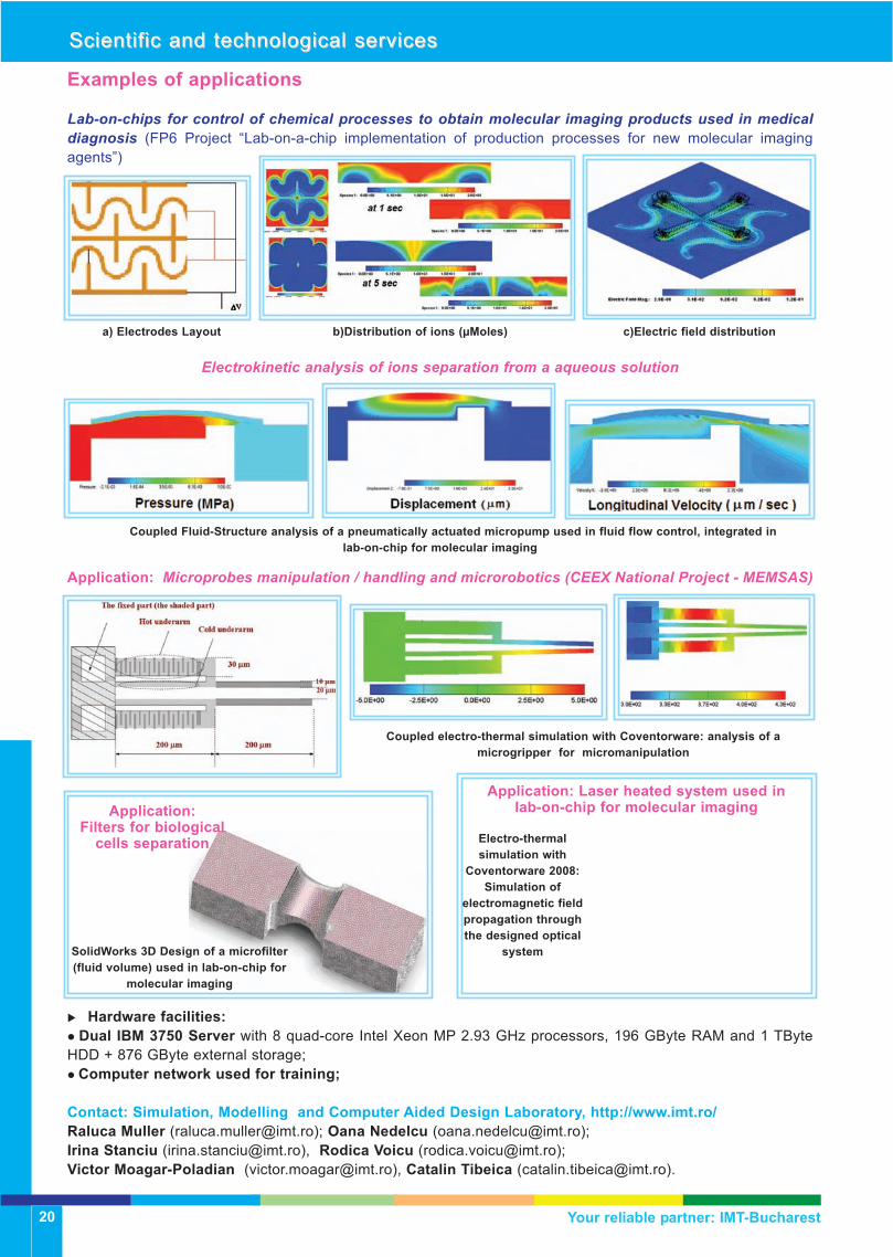
Examples of applications
Lab-on-chips for control of chemical processes to obtain molecular imaging products used in medicaldiagnosis (FP6 Project “Lab-on-a-chip implementation of production processes for new molecular imaging
agents”)
Electrokinetic analysis of ions separation from a aqueous solution
Application: Microprobes manipulation / handling and microrobotics (CEEX National Project - MEMSAS)
� Hardware facilities:
� Dual IBM 3750 Server with 8 quad-core Intel Xeon MP 2.93 GHz processors, 196 GByte RAM and 1 TByte
HDD + 876 GByte external storage;
� Computer network used for training;
Contact: Simulation, Modelling and Computer Aided Design Laboratory, http://www.imt.ro/
Raluca Muller ([email protected]); Oana Nedelcu ([email protected]);
Irina Stanciu ([email protected]), Rodica Voicu ([email protected]);
Victor Moagar-Poladian ([email protected]), Catalin Tibeica ([email protected]).
a) Electrodes Layout b)Distribution of ions (µMoles) c)Electric field distribution
Coupled Fluid-Structure analysis of a pneumatically actuated micropump used in fluid flow control, integrated in
lab-on-chip for molecular imaging
Application: Filters for biological
cells separation
Application: Laser heated system used in lab-on-chip for molecular imaging
SolidWorks 3D Design of a microfilter
(fluid volume) used in lab-on-chip for
molecular imaging
Electro-thermal
simulation with
Coventorware 2008:
Simulation of
electromagnetic field
propagation through
the designed optical
system
Coupled electro-thermal simulation with Coventorware: analysis of a
microgripper for micromanipulation
20

Scientific and technological servicesScientific and technological services
Your reliable partner: IMT-Bucharest
6. RAPID PROT6. RAPID PROTOTYPINGOTYPING
We may build any 3D body imagined by the customer by using selective laser sintering with the Formiga P100,
EOS (GmbH, Germany).
This object may be used for illustrative models, functional parts/end products and spare parts!
We offer two services for that purpose:
• CAD (Computer Aided Design) 3D modeling of the objects imagined by customer
• Physical realization of the respective objects
Description
• minimum size of the obtainable structures: 500 microns; • maximum building
volume: 200 mm x 250 mm x 330 mm; • minimum layer thickness: 100
microns;
Applications:
• Models realization (for engineering, architecture, education);
• Realization of molds for implants;
• Realization of molds for automotive industry, rubber industry (envelopes for
tyres), plastics industry, optical industry (special lenses and special mirrors),
medicine (prosthetics), museums (copies of sculptures that are very important), components for construction of
industrial machines, glass industry, porcelain industry;
• Realization of fix, mobile or semi-mobile mechanical components for specific applications, including robotics;
• Realization of microfluidics structures and circuits (channels of several hundreds of microns diameter,
connected in complex 3D geometries) containing pipes, valves, micropumps (at milimetric and centimetric scale);
• Realization of joining elements (screws, etc.) at milimetric scale;
• Realization of customized encapsulations for different type of MEMS structures;
• Realization of MEMS models for testing their concept and working principle;
3D Printer by using Selective Laser Sintering;
Materials used by 3D printer:
• PrimePart: Fine polyamid - biocompatible, excellent economics, withstands high mechanical and thermal load;
• PA 2200: Fine polyamid - biocompatible, withstands high mechanical and thermal load;
• PA 3200 GF: Glass-filled fine polyamide - hard-wearing, withstands high mechanical and thermal load;
• PrimeCast 101: Polystyrene - for lost patterns, minimal remaining ash content;
• PA 2210 FR: Flame-retardant polyamide - contains chemical flame retardant, high mechanical properties;
• PA 2201: Fine polyamid - withstands high mechanical and thermal load;
• Alumide: Aluminium-filled polyamid – stiff structures, thermally conductive;
• PS 2500: Polystyrene - for lost patterns;
Contact person: Dr. Phys. Gabriel Moagar-Poladian, [email protected]
Phys. Eng. Victor Moagar-Poladian, [email protected]
21

Competences in scientific researchCompetences in scientific research
Microsystem technologies
IMT-Bucharest mission is devoted to research and development in micro-and nano-technologies, reflected
by a rich experience in coordinating national networks, research and education projects, international
cooperation (participation in 15 FP6 EU Projects, 7 FP 7). IMT-Bucharest is integrating research, education and
technology transfer (innovation)-playing a national and regional role. The research laboratories of IMT-
Bucharest are involved in joint research with international and national partners, including SMEs, based on a
multidisciplinary approach, promoting the convergence of micro-nano-bio- info technologies. IMT-
Bucharest is involved in the development of several different types of microsensors and smart systems based
on microsystem technologies, which have become a key of innovation for traditional industrial sectors as well
as for new emerging technologies.
Main topics of research
� MEMS based microsensors and actuators for bio-medical, environmental applications and robotics: pressure
sensors, accelerometers, microgrippers;
� RF-MEMS devices and circuits: design, modelling and manufacturing of dielectric membrane supported
inductors, capacitors, filters and antennae based on silicon and GaAs micromachining; micromachined millimetre
and sub millimetre wave receiver modules, SAW interdigitated traducers;
� Photonic devices and MOEMS (waveguides, optical couplers, microring filters and resonators; grating-based
microstructures, tunable interferometers based on movable micromirrors, optical sensors), photonic circuits for
optical interconnections;
� CNT based micro-nanostructures for sensing and interconnections;
� Microfluidic devices;
� Biochips for biological materials investigation and detection (proteins, DNA, enzymes) on various substrates
(silicon, glass, polymers), microarrays, biosensors;
� Silicon nanoelectrode arrays, porous silicon layers (El, PL and bio-active properties); field emission
nanostructures;
� Magnetic nanostructures;
Apart from its formal executive structure in research laboratories, in IMT-Bucharest are active two centers:
� MIMOMEMS: European Centre of Excellence in Microwave, Millimetre Wave and Optical Devices,
based on Micro-Electro-Mechanical Systems for Advanced Communication Systems; Project No 202897
financed (2008-2010) through the “Regional potential” part (REGPOT call 2007-1). It has very strong links
(including exchange of researchers) by twinning with two important research centers in Europe: CNRS LAAS
Toulouse and IESL FORTH Heraklion.
� CNT-IMT: Centre of NanoTechnologies, under the aegis of the Romanian Academy of Sciences, which
is an interdisciplinary group, coupling activities in nanostructuring and nano-characterization of some research
labs from IMT. Starting January 2009, the Centre of NanoTechnologies CNT-IMT is extending his activities
becoming an interdisciplinary centre offering a variety of scientific and technological services in the
nanotechnology field
We present first the two centers and several examples of IMT competences in design/fabrication andcharacterization of microsensors and microsystems.
Scientific competences presented in this brochure are demonstrated also by the ISI publications, see details
on http://www.imt.ro/news
22
Competences in scientific researchCompetences in scientific research
Your reliable partner: IMT-Bucharest

Competences in scientific researchCompetences in scientific research
Your reliable partner: IMT-Bucharest
�� European Centre of Excellence MIMOMEMSEuropean Centre of Excellence MIMOMEMS
The overall aim of the MIMOMEMS project is to bring the research activity in RF and Optical-MEMS at the
IMT Bucharest to the highest European level. Two laboratories from IMT Bucharest (the Microwave and
Millimeter Wave Laboratory and the Microphotonics Laboratory) have joint their efforts to create this
European Center of Excellence.
After the first year of the MIMOMEMS project, the Scanning Near
field Optical Microscope (SNOM) the up-grade to 110GHz of the
existing 65 GHz set-up for “on wafer” millimetre wave
characterization and the frequency generator up to 110 GHz
(presented in page 16) are already working. An ongoing project in
the National Capacities program (“SIMCA”, http://www.imt.ro/simca)
has financed the spectrum analyzer up to 110 GHz and a white
light optical profilometer working in the Microwave laboratory.
Other new facilities have been obtained recently in the frame of
national programs by the technological department of IMT (a new MA6
/BA6 mask aligner, a laser pattern generator, a thin film deposition system
a RIE machine) and by the characterization department (the E-line Nano-
engineering workstation from Raith), a high performance SEM an XRD
equipment, a SPM equipment. All this equipments are included in the new
facility MINAFAB recently inaugurated by IMT, as a center of research and
services in micro and nanosystem fabrication and characterization in a new
clean room environment.
The technical and scientific objectives supported by the MIMOMEMS
project are: • millimeter wave receiving modules based on silicon and GaAs
micromachining;
• millimeter wave reconfigurable filters;
• acoustic devices for GHz applications based on GaN/Si and AlN/Si
micromachining and nanoprocessing;
• Polymer-based micro-photonic devices;
• Sub-wavelength photonic structures;
A new SAW structure manufactured on GaN/Si having the resonance at
7GHz. The structure was manufactured in cooperation by IMT and FORTHwith the support of the MIMOMES project. Nanolithography was performed
at IMT-Bucharest.
The first workshop devoted to the MIMOMEMS project
took place in October 2008. The second one (a strategic
workshop in MEMS for applications in microwave and
optical devices took place in October 2009 during the
Annual Semiconductor Conference of IMT (CAS 2009)
(http://www.imt.ro/cas)
Research equipments:
• Microwave network analyzer (0.04-65 GHz) with Manual
Probing Station-Lightning 37397D VNA/Anritsu; PM5/Suss
MicroTec (Anritsu, Japan; Suss MicroTec, Germany);
• Wafer Probing Station - Easyprobe EP4 (Suss
MicroTec, Germany);
• White Light Interferometer - Photomap 3D (FOGALE
nanotech, France);
• Scanning Near-field Optical Microscope - Witec alpha 300S (Witec, Germany);
Contact person: Dr Alexandru Muller, [email protected].
SAW structure manufactured on GaN/Si
having the resonance at 7 GHz
23
First acoustic devices operating at frequencies higher
then 7GHz, based on GaN/Si processing developed for
the first time in the world by IMT- Bucharest in
cooperation with FORTH Heraklion

�� Centre for Nanotechnologies CNTCentre for Nanotechnologies CNT-IMT-IMT
The Centre for Nanotechnologies was represented before 2009 by a single laboratory “Laboratory for
Nanotechnology” functioning as a centre of excellence under the aegis of the Romanian Academy. Now the
centre joined the activity of the following laboratories:
• Laboratory of Nanotechnology;• Laboratory for Nanoscale structuring and characterization; • Laboratory for Molecular nanotechnology;• Dip pen nanolithography Laboratory; • Laboratory for scientific services (will contribute to some extent);
The main specific activities of the centre consist in: • correlation of R&D activities and services of the
laboratories involved, also offering technical and financial support; • dissemination of the common offer towards
potential partners and beneficiaries outside IMT-Bucharest;
These laboratories offer state of the art facilities/equipments
concentrated in the technological area in the form of experimental
laboratories:
Grey AreaLaboratory of Nanotechnology:
• Experimental laboratory for “Microarrays” – NanoBioLab
• Experimental laboratory for surface spectroscopy• Experimental laboratory for X-Rays diffraction• Experimental laboratory for nanoparticles
Laboratory for nanoscale structuring and characterization
• Experimental laboratory for Electron Beam Lithography (EBL)/Scanning electron MicroscopyLaboratory (SEM) – NanoScaleLab
• Experimental laboratory for e-line work station• Experimental laboratory for SEM/FEG• Experimental laboratory for SPM
Laboratory for molecular nanotechnology
• Experimental laboratory for nanofluidics
Clean room area• Dip pen nanolithography Laboratory
Competences in scientific researchCompetences in scientific research
Your reliable partner: IMT-Bucharest24
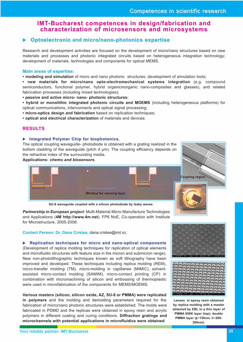
Competences in scientific researchCompetences in scientific research
Your reliable partner: IMT-Bucharest
IMTIMT-Bucharest competences in design/fabrication and -Bucharest competences in design/fabrication and characterization of microsensors and microsystems characterization of microsensors and microsystems
�� OptoelectronicOptoelectronic and micro/nano-photonics expertisemicro/nano-photonics expertise
Research and development activities are focused on the development of micro/nano structures based on new
materials and processes and photonic integrated circuits based on heterogeneous integration technology;
development of materials, technologies and components for optical MEMS.
Main areas of expertise:
• modeling and simulation of micro and nano photonic structures; development of simulation tools;
• new materials for micro/nano opto-electromechanical systems integration (e.g. compound
semiconductors, functional polymer, hybrid organicinorganic nano-composites and glasses), and related
fabrication processes (including mixed technologies);
• passive and active micro- nano- photonic structures;
• hybrid or monolithic integrated photonic circuits and MOEMS (including heterogeneous platforms) for
optical communications, interconnects and optical signal processing;
• micro-optics design and fabrication based on replication techniques;
• optical and electrical characterization of materials and devices;
RESULRESULTSTS
�� �� Integrated Polymer Chip for biophotonics. Integrated Polymer Chip for biophotonics.
The optical coupling waveguide- photodiode is obtained with a grating realized in the
bottom cladding of the waveguide (pitch 4 μm). The coupling efficiency depends on
the refractive index of the surrounding media.
Applications: chemo and biosensors.
Partnership in European project: Multi-Material Micro Manufacture Technologies
and Applications (4M http://www.4m.net), FP6 NoE, Co-operation with Institute
for Microstructure, 2005-2008.
Contact Person: Dr. Dana Cristea, [email protected];
�� �� Replication techniques for micro and nano-optical componentsReplication techniques for micro and nano-optical components
(Development of replica molding techniques for replication of optical elements
and microfluidic structures with feature size in the micron and submicron range).
New non-photolithographic techniques known as soft lithography have been
improved and developed. These techniques including replica molding (REM),
micro-transfer molding (TM), micro-molding in capillaries (MIMIC), solvent-
assisted micro-contact molding (SAMIM), micro-contact printing (CP) in
combination with micromachining of silicon and embossing of thermoplastic
were used in microfabrication of the components for MEMS/MOEMS.
Various masters (silicon, silicon oxide, AZ, SU-8 or PMMA) were replicated
in polymers and the molding and demolding parameters required for the
fabrication of micro/nano photonic structures were established. The molds were
fabricated in PDMD and the replicas were obtained in epoxy resin and acrylic
polymers in different coating and curing conditions. Diffraction gratings and
microchannels with potential applications in microfluidics were obtained
25
Window for sensing layer
Coupling region
SU-8 waveguide coupled with a silicon photodiode by leaky waves
Lenses in epoxy resin obtained
by replica molding with a master
obtained by EBL in a thin layer of
PMMA 950K layer (top); double
PMMA layer (φφ~150nm, h~200-
300nm).
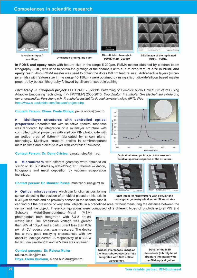
Competences in scientific researchCompetences in scientific research
Your reliable partner: IMT-Bucharest
in PDMS and epoxy resin with feature size in the range 5-200μm. PMMA master obtained by electron beam
lithography (EBL) was used to obtain the gratings or the channels with sub-micron feature size in PDMS and
epoxy resin. Also, PMMA master was used to obtain the dots (150 nm feature size). Antireflective layers (micro-
pyramids) with feature size in the range 40-150μm) were obtained by using silicon dioxide/silicon based master
prepared by optical lithography followed by silicon anisotropic etching.
Partnership in European project: FLEXPAET - Flexible Patterning of Complex Micro Optical Structures using
Adaptive Embossing Technology (IP- FP7/NMP) 2008-2010; Coordinator: Fraunhofer Gesellschaft zur Förderungder angewandten Forschung e.V. Fraunhofer Institut für Produktionstechnolgie (IPT). Web:
http://www.e-squizoide.com/flexpaet/project.php
Contact Person: Chem. Paula Obreja, [email protected];
�� �� Multilayer structures with controlled opticalMultilayer structures with controlled optical
properties:properties: Photodetector with selective spectral response
was fabricated by integration of a multilayer structure with
controlled optical properties with a silicon PIN photodiode with
an active area of 0.6mm2 fabricated by silicon planar
technology. Multilayer structure onsists in semitransparent
metallic films and dielectric layer with controlled thickness.
Contact Person: Dr. Dana Cristea, [email protected].
�� �� Micromirrors Micromirrors with different geometry were obtained on
silicon or SOI substrates by wet etching, RIE, thermal oxidation,
lithography and metal deposition by vacumm evaporation
technique.
Contact person: Dr. Munizer Purica, [email protected].
�� �� Optical microsensors Optical microsensors which can function as positioning
sensor detecting the position of an object placed on his axis in
0-300μm domain and as proximity sensor. In the second case it
can find out the presence of very small objects, in a predefined area, without measuring the distance between the
sensor and the object. These configurations were composed of 2 different types of photodetectors: PIN and
Schottky Metal-Semi-conductor-Metal (MSM)
photodiodes both integrated with SU-8 optical
waveguides. The breakdown voltage was greater
than 90V at 100μA and a dark current less than 0.02
nA at 5V reverse bias, was measured. The device
has a very good rectifying characteristic with low
absolute leakage current. A responsivity of 0.39A/W
for 630 nm wavelength and 20V bias was obtained.
Contact persons: Dr. Raluca Muller,
Phys. Elena Budianu, [email protected]
Microlens (epoxi)
φφ = 20 μμmDiffraction grating line 8 µm
Microfluidic channels in
PDMS width~250 nm
SEM image of the replicated
DOEin: PMMA.
Optical microscope image of the structure.
Relative spectral response of the structure.
SEM image of micromirrors with circular and
rectangular geometry obtained on Si substrates
Optical microscope image of
the linear photodetector arrays
integrated with SU8 optical
waveguides
Detail of the MSM
photodiode (interdigitated
structure integrated with
the SU-8 optical guide)
26

Competences in scientific researchCompetences in scientific research
Your reliable partner: IMT-Bucharest
�� RF MEMSRF MEMS
Main area expertise: • Development of a new generation of circuits devoted to the millimeter wave
communications based on the semiconductor (Si, GaAs, GaN) micromachining and nanoprocessing materials;
• Design and manufacturing of passive circuits elements, monolithically and hybrid integrated receiver front-
ends based on silicon and GaAs micromachining; • Acoustic devices (FBARs and SAWs) based on
micromachining and nanoprocessing of wide band gap semiconductors (AlN, GaN); • Microwave devices based
on carbon nanotubes; • Microwave devices using CRLH materials (metamaterials); • MEMS and NEMS
technologies developement;
�� �� 77 GHz millimeter wave receiver module77 GHz millimeter wave receiver module based on the hybrid
integration of a SiO2/Si3N4 membrane supported Yagi-Uda antenna with GaAs
Schottky detector diode. Design, modeling and manufacturing of 77GHz silicon
micromachined receiver structures. The design procedure, the technological
processing and characterization techniques open a window of opportunity for
the development of innovative architectures for circuits and systems operating
at higher frequency, up to the sub-millimetre wave frequency range. The
membrane supported millimeter wave receiver operating in the 60GHz
frequency range was and characterized. The receiver structure is based on the
hybrid integration of a Yagi-Uda antenna with a Schottky diode, the antenna
having as support a 1.5 μm thin SiO2/Si3N4 dielectric membrane. Results obtained in the frame of "ACOMEMS
Integrated RF-MEMS circuits based on silicon, gallium arsenide and wide band gap semiconductors for advanced
communication systems", CEEX Project (2005-2008). Web: http://www.imt.ro/acomems
�� �� WWide band gap semiconductor SAide band gap semiconductor SAW type devices for GHzW type devices for GHz
applicationsapplications, manufactured using nanolithographic techniques. A SAW
structure for an operating frequency of about 2.8GHz was successfully
developed on a thin AlN layer sputtered on high resistivity silicon. The
structures were obtained with the support of the Nanoscale-Conv Project (Nr
6111/2005-CALIST). Experiments to develop SAW structures with operating
frequencies in the GHz range were performed on AlN and GaN thin films with
nano-metric lines for an interdigitated transducer (IDT). After the
nanolithography there were obtained some very good quality inerdigitated
Ti/Au structures (with 30 digits and 29 interdigits 300nm wide, 220nm high and
200μm long). Lift-off techniques to remove the undesired metal were used. On wafer microwave measurements of
the SAW structure have demonstrated its functionality. It was evidenced a pronounced resonance at about 2.8GHz.
Results obtained in the frame of "ACOMEMS” Project.
�� �� GaN based resonator on high resistivityGaN based resonator on high resistivity
<111> silicon substrate for operation around 1.2 GHz
has been fabricated using micromachining techniques.
Resonator structuresResonator structures of this type can be used as
building blocks for the fabrication of high Q and wide
bandwidth filters, for use in reconfigurable front-ends of
various mobile and wireless applications. Results
obtained in the frame of "ACOMEMS” Project.
Contact person: Dr. Alexandru Muller, [email protected];
�� �� Nanoelectronics based carbon nanotubes. Nanoelectronics based carbon nanotubes. The design of test structures
for CNT characterization, experiments regarding CNT manipulation of CNT and dc
characterization technological implementation of the microwave test structures were
succesfully performed. Achievements: the interconnection of a CNT bundle over a
dielectric trench. Results obtained in the frame of the PN II Project "Nanoelectronic
devices for high frequencies based on carbon nanostructures for communications
and environment monitoring" (2007-2010). Web http//:www.imt.ro/nano-hf
Contact person: Dr. Mircea Dragoman, [email protected];
Optical photo of the 77 GHz receiver
structure micromachined on a
SiO2/Si3N4 membrane
Two experimental SAW structures
with the two IDTs placed “face to face”
SEM photo (top side) of the
GaN membrane supported F-
BAR structure. The silver
epoxy on the left side is used in
order to provide a connection of
the ground electrode to the
bottom metallization of the
FBAR membrane and allow
measurements with GSG probes
A FET-like configuration based
CNT
27

Competences in scientific researchCompetences in scientific research
Your reliable partner: IMT-Bucharest
�� MICROSENSORSMICROSENSORS
Main area expertise: • Sensors: chemoresistive, resonant gas sensors, accelerometers, microarrays, ISFET
(Ion Sensitive Field Effect Transistors) sensors, electrodes for biological sensors, microprobes for recording of
electrical activity of cells and tissues; • Materials development for sensors and packaging;
�� �� Microfluidic Pesticide Biosensor:Microfluidic Pesticide Biosensor:
• based on silicon chip and acetylcholinesterase biomaterial.
• sensitivity is in the range of 10-9M-10-6M.
• is reacting at organophosporus compounds that can be found in food, water,
drugs, soil, vegetables, fruits.
• is fast and the overall preparation and measuring operation can be done in less of
˝ hour.
The biosensor is placed into the microfluidic module which allows the
preparation of the sensor by injection of the electrolyte, the introduction of the
sample and the electrical signal recording by using 4 spring probes connecting
the biosensor pads with the measuring instruments. IMT is offering the siliconchip, the electrolytes and the specifications for sensor preparation andmeasuring. The sensor is a consumable one and needs to be removed after
every detection step. According to customers requests the pH and temperature
can be monitored inside the microchannels. A pH and a temperature sensor will
be placed close to biosensor side. EPIGEM is offering the microfluidic module
hosting the silicon biochip. According to customer requirements, a heating
module can be developed, for keeping the sensor at 370C during its life time.
IMT is offering the pesticide sensor, the Labview interface, the heating module and the microelectronics modulefor signal conditioning. The measurements will be computer controlled and data acquisition can be achieved. The
silicon chip is based on interdigitated electrodes 6x12mm which are deposited with acetylcholinesterase enzyme.
• Partnership in “INTEGRAMplus” - Multi-domain platforms for integrated micro-nano technology systems, IP,
Priority 2 -IST, Contract no.: 027540 (2006-2008), Coordinator: QinetiQ Ltd, UK. IMT position: partner;
Project web: http://www.integramplus.com/
• Results obtained also in the frame of the project: “Miniaturized immunosensor arrays technology, for herbicide
detection” IMUNOSENSE, PNII national project. Web: http://www.imt.ro/imunosense/
Contact Person: Dr. Carmen Moldovan, [email protected]
�� �� Integrated microfluidic system for advanced in vitro biochemical analysis for diagnostic andIntegrated microfluidic system for advanced in vitro biochemical analysis for diagnostic and
treatment in medical applications treatment in medical applications
The microfluidic device incorporates a sampling, dispensing and delivering system for magnetic marked
biomolecules or with intrinsic magnetic properties, and it consists of two main modules. The first module contains:
a rotary viscosimeter, for viscosity measurements; microchannels with input and output reservoirs for fluid transport
and a microfluidic platform that can trap, measure, manipulate and sort magnetic marked biomolecules in an array
of magnetophoretic spin valves. The second module is the detection and measurement magnetoelectronic systemconsisting of a double Wheatstone bridge with four sensing GMR resistors and four reference shielded GMR
resistors. This magnetic microsystem could detect the presence of bioparticles or microbeads. These microdevices
enjoy the advantage of being compatible with silicon IC fabrication technology. It is possible to build an array of
GMR sensing elements that can simultaneously tests multiple biological molecules. The originality consists of
extracting information regarding molecular interactions and rheological properties of the biological non - Newtonian
fluids from a single microsystem.
• Results obtained also in the frame of the project: MICRO-DIAG - Integrated Microfluidic Systems for Advanced in
vitro Biochemical Analysis for Diagnostic and Treatment in Medical Applications/ Sistem microfluidic integrat pentru
analiza in vitro a fluidelor biologice cu aplicatii in diagnoza si tratament medical, 2005-2008, Web
http://www.imt.ro/Microdiag/
Contact Person: Dr. Marioara Avram, [email protected]
Silicon chip based on
interdigitated electrodes
Silicon biochip into the microfluidic
module, pumps and reservoirs
28

Competences in scientific researchCompetences in scientific research
Your reliable partner: IMT-Bucharest
�� �� Microsensor:Microsensor: New technology for microbiosensors for real time detecting and monitoring tuberculosis.
• Differential SAW piezoelectric microsensor development with lay-out designed to increase sensitivity and
selectivity;
• Processing of the tantalate and langasite substrates;
• Microsensors assembly using reusable support;
Results obtained in the frame of the project
MICROBALERT-“New technologies for achieving
microbiosensors for real time detecting and monitoring
tuberculosis in groups with increased risk potential”,
CEEX 2006-2008. Web: http://www.imt.ro/microbalert
�� �� Materials and Packaging: Materials and Packaging: New materials and micro/nanosensors technologies developmentNew materials and micro/nanosensors technologies development
�� �� Advanced nanocomposites materials used in civil construction with antibacterial properties for ambiental
improvement. It has been developed a new construction
material, a “smart wall”, from composites cement-wood. Thin
polymeric composites films with oxide nanopowders content
(having antibacterial, antistatic tailored proprieties) and solar
concentrators were applied.
Results obtained in the frame of the project NANOAMBIENT
Advanced Nanocomposites materials used in civil
constructions with antibacterial, selfcleaning properties and
solar energy concentrators integrated structures for ambiental
improvement (http:www.imt.ro/nanoambient).
Contact Person: Ileana Cernica, [email protected].
�� �� New MCM packaging technique for PIN microdetectors matrix with improved technological processes for
optimized performances in transmission and direct coupling to the optical cable.
Characteristics: • a silicon wafer used for PIN detectors assembly;
• optimized 2 masks technology;
• two steps anisotropic silicon etching for lowering the roughtness;
• 50μm thick bronze-beryllium support used as ground palne for the micromatrix and also for
configure the external pin connection of the micromatrix.
Contact Person: Ileana Cernica, [email protected].
Sensor for detection of TB
on langasite substrateType of connectors
proposed for sensors
1 Cement-wood composite substrate
2 Polymeric films with doped nanopowder
29
�� Simulation/modelling competencesSimulation/modelling competences
�� �� Design: Design: A new design was developed
for a polymeric microgripper, which can
realize a movement of the gripping arms
with possibility for positioning and
manipulating of the gripped object. Two
models of the microgripper, electro-thermo-
mechanical actuated, using low actuation
voltages, designed for SU-8 polymer
fabrication were investigated and
compared. Finite-element analyses (FEM),
using COVENTOR-WARE 2008 tool, were
performed in order to evaluate the relation
between the displacement, temperatures
and the electrical current passing through
the metallic layers.
Contact person: Mat. Rodica Voicu, [email protected]
�� �� Simulation: Simulation: New materials need
to be used in industrial fields by
providing protection against harsh
environments (high temperature,
aggressive chemical agents, abrasion,
thermal and mechanical shocks, etc.).
Simulations regarding the protective
layer behaviour in contact with different
types of aggressive agents were
performed. Due to the complexity of
the problem, the software used was
ANSYS Multiphysics 11.0.
Contact person Victor Moagar-
Poldian, [email protected]
�� �� Computer aided design for microfluidic componentsComputer aided design for microfluidic components
The project scope was to develop new design of microfluidic
components, particularly micromixers.
Results: Micromixers have been designed simulated and fabricated
microfabricated in polymer (SU-8)
Contact persons: Mat. Irina Stanciu, [email protected];
Mat. Oana Tatiana Nedelcu, [email protected].
Competences in scientific researchCompetences in scientific research
Your reliable partner: IMT-Bucharest
Maximal values of the
temperatures in the
microgripper when a voltage of
0.25 V is applied-simulation with
CoventorWare tool
Design of the half of microgripper
model without the SU-8 layer on
the 0.25V is applied- simulation
with CoventorWare tool
Layer integrity and summed deformation
after impact is presented. The numbers
above the figures are representing the
angle, speed and diameter of the impacting
particle. Home made Monte Carlo
simulation software (based on ANSYS
simulations), providing the number of
colision until protective layer penetration
Velocity distribution in a micromixer using
comsol software
30
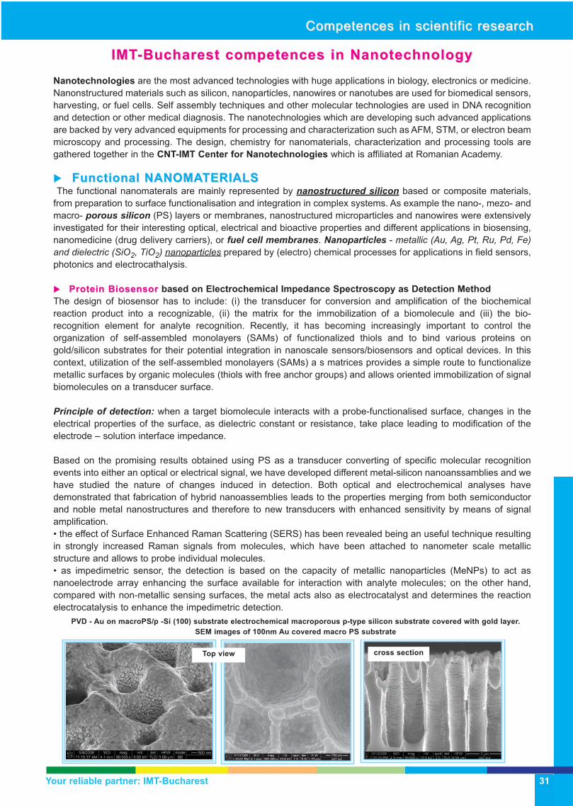
Competences in scientific researchCompetences in scientific research
Your reliable partner: IMT-Bucharest
IMTIMT-Bucharest competences in Nanotechnology-Bucharest competences in Nanotechnology
Nanotechnologies are the most advanced technologies with huge applications in biology, electronics or medicine.
Nanonstructured materials such as silicon, nanoparticles, nanowires or nanotubes are used for biomedical sensors,
harvesting, or fuel cells. Self assembly techniques and other molecular technologies are used in DNA recognition
and detection or other medical diagnosis. The nanotechnologies which are developing such advanced applications
are backed by very advanced equipments for processing and characterization such as AFM, STM, or electron beam
microscopy and processing. The design, chemistry for nanomaterials, characterization and processing tools are
gathered together in the CNT-IMT Center for Nanotechnologies which is affiliated at Romanian Academy.
�� Functional NANOMAFunctional NANOMATERIALSTERIALSThe functional nanomaterals are mainly represented by nanostructured silicon based or composite materials,
from preparation to surface functionalisation and integration in complex systems. As example the nano-, mezo- and
macro- porous silicon (PS) layers or membranes, nanostructured microparticles and nanowires were extensively
investigated for their interesting optical, electrical and bioactive properties and different applications in biosensing,
nanomedicine (drug delivery carriers), or fuel cell membranes. Nanoparticles - metallic (Au, Ag, Pt, Ru, Pd, Fe)and dielectric (SiO2, TiO2) nanoparticles prepared by (electro) chemical processes for applications in field sensors,
photonics and electrocathalysis.
�� �� Protein BiosensorProtein Biosensor based on Electrochemical Impedance Spectroscopy as Detection Method
The design of biosensor has to include: (i) the transducer for conversion and amplification of the biochemical
reaction product into a recognizable, (ii) the matrix for the immobilization of a biomolecule and (iii) the bio-
recognition element for analyte recognition. Recently, it has becoming increasingly important to control the
organization of self-assembled monolayers (SAMs) of functionalized thiols and to bind various proteins on
gold/silicon substrates for their potential integration in nanoscale sensors/biosensors and optical devices. In this
context, utilization of the self-assembled monolayers (SAMs) a s matrices provides a simple route to functionalize
metallic surfaces by organic molecules (thiols with free anchor groups) and allows oriented immobilization of signal
biomolecules on a transducer surface.
Principle of detection: when a target biomolecule interacts with a probe-functionalised surface, changes in the
electrical properties of the surface, as dielectric constant or resistance, take place leading to modification of the
electrode – solution interface impedance.
Based on the promising results obtained using PS as a transducer converting of specific molecular recognition
events into either an optical or electrical signal, we have developed different metal-silicon nanoanssamblies and we
have studied the nature of changes induced in detection. Both optical and electrochemical analyses have
demonstrated that fabrication of hybrid nanoassemblies leads to the properties merging from both semiconductor
and noble metal nanostructures and therefore to new transducers with enhanced sensitivity by means of signal
amplification.
• the effect of Surface Enhanced Raman Scattering (SERS) has been revealed being an useful technique resulting
in strongly increased Raman signals from molecules, which have been attached to nanometer scale metallic
structure and allows to probe individual molecules.
• as impedimetric sensor, the detection is based on the capacity of metallic nanoparticles (MeNPs) to act as
nanoelectrode array enhancing the surface available for interaction with analyte molecules; on the other hand,
compared with non-metallic sensing surfaces, the metal acts also as electrocatalyst and determines the reaction
electrocatalysis to enhance the impedimetric detection.
PVD - Au on macroPS/p -Si (100) substrate electrochemical macroporous p-type silicon substrate covered with gold layer.
SEM images of 100nm Au covered macro PS substrate
Top view cross section
31
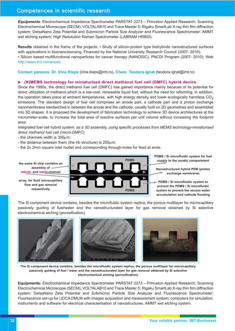
Equipments: Electrochemical Impedance Spectrometer PARSTAT 2273 – Princeton Applied Research; Scanning
Electrochemical Microscope (SECM), VOLTALAB10 and Trace Master 5; Rigaku SmartLab X-ray thin film diffraction
system; DelsaNano Zeta Potential and Submicron Particle Size Analyzer and Fluorescence Spectrometer; AMMT
wet etching system; High Resolution Raman Spectrometer (LABRAM HR800).
Results obtained in the frame of the projects: • Study of silicon-protein type biohybride nanostructured surfaces
with applications in bio(nano)sensing, Financed by the National University Research Council (2007- 2010);
• Silicon based multifunctional nanoparticles for cancer therapy (NANOSIC), PNCDI Program (2007- 2010); Web
http://www.imt.ro/nanosic
Contact persons: Dr. Irina Kleps ([email protected]), Chem. Teodora Ignat ([email protected])
�� �� (N)MEMS technology for miniaturized direct methanol fuel cell (DMFC) hybrid device(N)MEMS technology for miniaturized direct methanol fuel cell (DMFC) hybrid device
Since the 1990s, the direct methanol fuel cell (DMFC) has gained importance mainly because of its potential for
direct utilization of methanol,which is a low-cost, renewable liquid fuel, without the need for reforming; in addition,
the operation takes place at ambient temperatures, with high energy density and lower ecologically harmless CO2
emissions. The standard design of fuel cell comprises an anode part, a cathode part and a proton exchange
nanomembrane sandwiched in between the anode and the cathode, usually built on 2D geometries and assembled
into 3D shapes. It is proposed the development of fabrication technology to achieve 3D device architectures at the
micrometer-scale, to increase the total area of reactive surfaces per unit volume without increasing the footprint
area.
Integrated fuel cell hybrid system, as a 3D assembly, using specific processes from MEMS technology-miniaturiseddirect methanol fuel cell (micro-DMFC)- the channels width is 300μm;
- the distance between them (the rib structure) is 250μm;
- the 2x 2mm square inlet /outlet and corresponding through-holes for feed at ends.
The Si component device contains, besides the microfluidic system replica, the porous multilayer for microcapillary
passively guiding of fuel/water and the nanostructurated layer for gas removal obtained by Si selective
electrochemical etching (porosification)
Equipments: Electrochemical Impedance Spectrometer PARSTAT 2273 – Princeton Applied Research; Scanning
Electrochemical Microscope (SECM), VOLTALAB10 and Trace Master 5; Rigaku SmartLab X-ray thin film diffraction
system; DelsaNano Zeta Potential and Submicron Particle Size Analyzer and Fluorescence Spectrometer;
Fluorescence set-up for LEICA DMLM with images acquisition and measurement system; computers for simulation;
instruments and software for electrical characterisation of nanostructures. AMMT wet etching system.
Competences in scientific researchCompetences in scientific research
Your reliable partner: IMT-Bucharest
the same Si chip contains an
assembly of
micro- and nano-channel
array, for fluid microcapillary
flow and gas removal
respectively
PDMS / Si microfluidic system for fuel
supply to the anodic compartment
Nanostructured hybrid PEM (proton
exchange membrane)
PDMS / Si microfluidic system to
prevent the PDMS / Si microfluidic
system to prevent the excess water
accumulation and cathode flooding
Si
Si
PDMS
PDMS
The Si component device contains, besides the microfluidic system replica, the porous multilayer for microcapillary
passively guiding of fuel / water and the nanostructurated layer for gas removal obtained by Si selective
electrochemical etching (porosification)
32

Competences in scientific researchCompetences in scientific research
Your reliable partner: IMT-Bucharest
Results obtained in the frame of the projects: • Study of membrane - electro-catalyst nanocomposite assemblies
on silicon for fuel cell application; Financed by the National University Research Council (2007- 2010);
• Miniaturised power source for portable electronics realised by 3d assembling of complex hybrid micro- and
nanosystems (MINASEP); PNCDI Program (2007- 2010); Web: http://www.imt.ro/minasep
Contact Person: Dr. Mihaela Miu, [email protected]
�� �� Electrocatalytic activity of Pt and Pt-alloy nanoparticlesElectrocatalytic activity of Pt and Pt-alloy nanoparticles
The general context: The proton exchange membrane (PEM)/electro-catalyst assembly represents the central
compartment of the miniaturized fuel cell, where the electrochemical reactions take place, and also the produced
ionic charges are conducted between the electrodes and thereby complete the cell electric circuit. A new metallic-
semiconductor nanosystem on Si has been studied for potential integration in a micro fuel cell as membrane
electrode assembly (MEA) using specific processes to nano- micro-electromechanical system (N/MEMS)
technology. Silicon membrane has been subjected to an electrochemical process which determines the
porosification/nanostructuring and consequently the increase of the geometry surface area and the density of
chemically active sites. Si membrane morphology depends on process parameters, and the pores diameter can be
tuned from nm to µm.
Equipments: Electrochemical Impedance Spectrometer PARSTAT 2273 – Princeton Applied Research; Scanning
Electrochemical Microscope (SECM), VOLTALAB10 and Trace Master 5; Rigaku SmartLab X-ray thin film diffraction
system; DelsaNano Zeta Potential and Submicron Particle Size Analyzer and Fluorescence Spectrometer;
Fluorescence set-up for LEICA DMLM with images acquisition and measurement system; computers for simulation;
instruments and software for electrical characterisation of nanostructures.
Results obtained in the frame of the projects: • Study of membrane - electro-catalyst nanocomposite assemblies
on silicon for fuel cell application; Financed by the National University Research Council (2007- 2010);
• Miniaturised power source for portable electronics realised by 3d assembling of complex hybrid micro- and
nanosystems (MINASEP); PNCDI Program (2007- 2010); Web: http:www.imt.ro/minasep
• Silicon based multifunctional nanoparticles for cancer therapy (NANOSIC), PNCDI Program (2007- 2010);
Web:http:www.imt.ro/nanosic
Contact Person: Dr. Mihaela Miu ([email protected])
�� �� Nanostructured microcarriers based on silicon for drug deliveryNanostructured microcarriers based on silicon for drug delivery
The aim of this work is to optimise the experimental
conditions for nanostructured Si particles fabrication
and to find the best methods for attaching on its
surface cytotoxic molecules of therapeutic interest. In
order to survey the biocompatibility of silicon, local
and general tolerance on animals has been
investigated. General tolerance was monitored by
physiological aspects, weight gain, oxidative stress
and biological markers. Macroscopic and histological
examination of muscles and derma inoculation areas
tissues were used as indexes of local tolerance.
Pt nanoparticles/Porous silicon (PS). A Pt precursor solution (3.5mM H2PtCl6)
was used for chemical impregnation. Also mixture of Pt and Au, Pt and Fe
solutions have been used.
Si microparticles with nano-
porous structure obtained after
wet ball mill treatment (1h)
PS multilayers obtained on p+
Si (top view and cross section)
33

CONCLUSIONS: Nanosilicon particles investigated as carriers for drug delivery are well tolerated by animal body.
At molecular level, there were observed both amplifications of detoxification and of oxidative stress systems that
represent normal responses to xenobiotics.
Results obtained in the frame of the project: • Silicon based multifunctional nanoparticles for cancer therapy
(NANOSIC), PNCDI Program (2007- 2010); Web: http:www.imt.ro/nanosic
Contact Person: Dr. Irina Kleps, [email protected]
�� Molecular-scale technologiesMolecular-scale technologies
Molecular-scale technologies: functional interfaces between biological materials (from individual biomolecules to
cells) and inorganic surfaces: molecular nanofabrication by self-assembly (thiols/Au) and supramolecular systemsthrough self-organization concepts (polyelectrolyte multilayer membranes assembled by layer-by-layer technique);
biosensing core-shells NPs (biotine/avidine/APTS/Au), grafting of (bio)molecules on various surfaces (protein or
DNA/glass, Si, PS for biomolecular recognition) with applications in microarrays and immunologic sensors for
medical diagnosis. Technologies/devices such as microarrays, biosensors for biological material investigation and
detection (proteins, DNA, enzymes) are developed on various substrates (silicon, glass, polymers).
�� �� CRPCRP immobilization on nanostructured siliconimmobilization on nanostructured silicon
Protein microarrays have remarkably evolved in the last decade and became one of
the main tools for proteomic studies. The porous surfaces have proven to be a very
attractive substrate for protein microarrays, because they offer a three dimensional
structure, thus enlarging proprieties and spot confinement.
Porous silicon substrate manufacture: Porous silicon (PS) layer was obtained by
electrochemical etching of silicon p type substrate (100) crystallographic orientation
with 5-10Ωcm resistively using HF electrolyte solution (1:1 in ethanol or water:
ethanol) for 300s. SEM image presented as result two PS samples with pore size 10-
20nm.
Results: The PS surfaces were used for the immobilization of two Cy3
labelled CRP human antibodies: monoclonal rabbit (anti-mCRP) and
polyclonal goat (anti-pCRP). Four different antibodies concentrations
(between 0.75 mg/mL and 0.21875mg/mL, serial dilutions) were printed in
various buffers (phosphate buffered saline (PBS), 0.25 M citrate in PBS,
commercial printing buffer), using the same conditions of temperature and
humidity. The slides were incubated overnight and thoroughly washed with
PBS and deionized water.
Equipments: Plotter microarray (GeneMachines OmniGrid Micro) and
Scanner microarray (GeneTAC UC4); Electrochemical Impedance
Spectrometer PARSTAT 2273-Princeton Applied Research; Scanning
Electrochemical Microscope (SECM), VOLTALAB10 and Trace Master 5;
Rigaku SmartLab X-ray thin film diffraction system; Fluorescence
Spectrometer; Fluorescence set-up for LEICA DMLM with images acquisition and measurement system; computers
for simulation; instruments and software for electrical characterisation of nanostructures.
Results obtained in the frame of the project: • DNASIP - A “system-in-a-microfluidic package” approach for focused
diagnostic DNA microchips. ERA – NET project; • Multi alergen biochip realised by microarray technology (MAMA),
PNCDI Program (2007- 2010). Web: http://www.imt.ro/mama
Contact Person: Phys. Monica Simion, [email protected]
Competences in scientific researchCompetences in scientific research
Your reliable partner: IMT-Bucharest
SEM image of PS onto
which aCRP was
immobilized
a) Solid pin size: 200 microns
Spot sizes: 200-200 microns, distance
between spots 100 microns
d) Scanned image with immobilized
fluorescent antibodies on the two PS
surfaces
34

Competences in scientific researchCompetences in scientific research
Your reliable partner: IMT-Bucharest
�� �� Layer-by-layer Layer-by-layer deposition technique for hybrid nanostructures
A new technique has been developed at IMT, layer-by-layer technology
(LbL) based on deposition of electrically charged thin films. It consists in
sequential absorption of positive and negative electrically charged
species, called cationic and anionic polyelectrolytes, by alternative
immersions into solutions of these polyelectrolytes. This technique relies
on the electrostatic force of attraction assuring also a strong adhesion
between the anionic and cationic layers. We prepared a multilayer
polyelectrolyte film using Nafion 117 membrane as substrate and poly
(sodium styrene sulfonate)-PSS, as polyanion and poly(diallyl
dimethylammonium chloride)-PDDA, as polycation. The figure shows UV-vis spectra of the LbL self-assembled
Nafion 117 membrane as a function of the number of PDDA-PSS bilayers. For PDDA-PSS multilayers although the
absorbance peak at 225 nm was not shown clearly, the absorbance increased with an increased number of bilayers.
Layer-by-layer technique can be used for surface modification and also, for fabrication of thin film devices-
permitting multimaterial assemblies including proteins and colloids, with applications in anticorrosion,
biocompatibility, fuel cell, biosensors, implants, optical waveguides, electroluminescent devices, microreactors.
Equipments: Electrochemical Impedance Spectrometer PARSTAT 2273-Princeton Applied Research; Scanning
Electrochemical Microscope (SECM), VOLTALAB10 and Trace Master 5; Fluorescence Spectrometer;
Fluorescence set-up for LEICA DMLM with images acquisition and measurement system; computers for simulation;
instruments and software for electrical characterisation of nanostructures.
Results obtained in the frame of the projects: • Silicon based multifunctional nanoparticles for cancer therapy
(NANOSIC), PNCDI Program (2007- 2010); Web: http:www.imt.ro/nanosic;
• Study of membrane - electro-catalyst nanocomposite assemblies on silicon for fuel cell application. Financed by
the National University Research Council (2007- 2010)
Contact Person: Chem. Adina Bragaru, [email protected].
�� SStructuring at nanoscaletructuring at nanoscale
�� �� Using e-line EBL nanoengineering workstation from RAITHnanoengineering workstation from RAITH, which
is a versatil equipment for nanolitography with specific requirements for
interdisciplinary research (EBID and EBIE: electron beam induced deposition
and etching) we can develop nanosale devices.
We have fabricated two-dimensional photonic crystals (PCs) obtained by direct
patterning of positive PMMA electronoresist, using the Electron-Beam
Lithography technique (EBL). The fabrication of the device was a challenge
because we integrated the PC waveguide configuration with a taper optical waveguide on the same substrate.
NANOSCALE-CONV (2005-2008); Project type: PN II CEEX; No. 6111/2005
Contact: Dr.Raluca Müller, [email protected]; Phys. Adrian Dinescu, [email protected].
�� �� Polymer nanowire electrically contacted using EBIDPolymer nanowire electrically contacted using EBID
Results obtained in cooperation: IMT-
Bucharest with Katholieke Universiteit
Leuven.
Contact person:
Phys. Adrian Dinescu,
[email protected] obtained using
conventional litogrtaphy and EBID
for 4 probes measurements of
electrical properties of a polymer
nanowire
Polymer nanowire electrically
contacted using EBID
SEM photos of the
experimental PC structures
35

Education Education
�� New Master (M. Sc. Courses) at the Faculty for
Electronics, Communications and Information Technology,
University “Politehnica” of Bucharest starting October 2009 and
held in IMT (with access to experimental facilities).
• Microsystems:• Microsystems:
- Intelligent sensors and microsystems;
- Microphysical characterization of structures;
• Micro- and Nanoelectronics: • Micro- and Nanoelectronics:
- Advanced Technological Processes
• Electronic T• Electronic Technology for Medical echnology for Medical Applications:Applications:
- Micro- and Nanotechnologies for Medical
Applications
�� Postdoc program: A Postdoc program in the areas of RF MEMS and MOEMS financed by FP7
MIMOMEMS project was launched in 2009 in IMT. Three postdocs were employed in IMT up to now.
�� Other educational actions within different projects:
• • FP 6: ASSEMIC - Marie Curie Training Network (2004-2007), Contract No. MRTN-CT-2003-504826,
supervising the activity of PhD students and post doc.
• • 2 Leonardo da Vinci -Life Long Learning projects, where IMT was partner:
-“Microteaching Project” (2004-2007), coordinated by RWTH Aachen University
-“Development of competences of educational staff by integrating operational tasks into measures of vocationaltraining and further education" ComEd, (2008-2010) coordinated by BWAW Thüringen gGmbH, Germany
• • Short courses regarding microtechnologies were developed and presented to SMEs.
• • Intership (3 months in 2007) for a student from INSA-Toulouse, France
�� Simulation, consulting and training services in micro and nano domains;
�� �� Computer Aided Design using dedicated software
tools: COVENTOR 2008 and ANSYS
• • Mask Design, Process Editor, 3D building and mesh;
• • Modeling for technological processes/optimizations;
• • Special features: particularized use (macro or
subroutine) creation; special geometrical modeling (AFM
images reconstruction in CAD format, surfaces generated
in accordance with mathematical expression, etc);
�� �� Computer Aided Engineering and Analysis (using
FEM, FVM, BEM tools);
• • Microfluidics analysis (thermo)dynamics, electro-
kinetics, diffusion, fluid mixing and separation in micro-
components;
• • Electro-thermo-mechanical and piezoelectric
analysis (steady state and transient).
• • Coupled field simulations: thermo-mechanical simulations; electro-mechanical simulations; multiphysics,
fluid-solid interaction;
�� �� Consultancy regarding design and simulation optimization;
�� �� Training in COVENTOR COMSOL and ANSYS using training dedicated infrastructure;
EducationEducation
Your reliable partner: IMT-Bucharest36
Training room for courses and services in MEMS design,
modelling and simulation

TTechnological echnological TTransfer Infrastructuresransfer Infrastructures
Your reliable partner: IMT-Bucharest
CENTRE FOR TECHNOLOGYCENTRE FOR TECHNOLOGY TRANSFER INTRANSFER INMICROENGINEERING (CTTMICROENGINEERING (CTT-Baneasa)-Baneasa)
CTT-Baneasa was established by IMT-Bucharest in 2003 and was accredited as an autonomous entity in March
2006. The major mission of the Center is to develop the micro- nanotechnologies domain, by stimulating the
technological transfer and innovation at national level, and by interacting with European entities.
CTT Baneasa must assure a critical amount regarding knowledge and technological transfer in the field of micro-
and nanoengineering, taking into consideration only the offers from Romanian research entities regarding this
field.
The Centre has adopted 4 driving strategies for continuously effective technology transfer and commercialization:
• identification of market needs by: market research, selection of target industries, and evaluation of technology
trends;
• potential evaluation and effort driving in collaboration with the R&D groups to optimally address the real
industrial needs and requirements, by: active contact, focused information feeding and informed advice;
• actively promoting the R&D outcome, by: identifying and participating in most relevant technology transfer and
promotion events (exhibitions, innovation salons, conferences, seminars, brokerages, workshops), or
encouraging the authors to attend; publishing newsletters through networking channels; creating and distributing
promotion materials;
• participation to emerging opportunities, by: partnerships with technology transfer intermediaries worldwide;
identifying/establishing/maintaining contact with decision factors from relevant enterprises and keeping them
informed via focused electronic information materials; CTT- Baneasa has a key role as intermediator regarding
valorisation of the research projects obtained results.
Participation to fairs and exhibitions:
• Hannover International Industrial Fair HANNOVER
MESSE, 21-25 April 2008, Hanover, Germany;
• European Research and Innovation Exhibition in Paris
(the fourth edition), 5- 7 June 2008, France;
• International Inventors Exhibition from Croatia- ARCA, 16-
21 September 2008, Zagreb, Croatia;
• INNOVA Exhibition- Bruxelles International Contest-
EUREKA, dedicated to inventics, 13- 15 November 2008,
Bruxelles (2 Gold Medals);
• INVENTIKA Exhibition 2008, 7- 11 October 2008,
Bucharest (1 Gold Medal, 1 Silver Medal and 2
Bronze Medals);
• Research Exhibition 2008, 7- 11 October 2008,
Bucharest, Romania;
• Research Exhibition 2008, 20- 23 November 2008,
Bacau, Romania;
For these actions, CTT-Baneasa elaborated
advertising materials, identified and promoted services and technologies corresponding with the domains
proposed for IMT, companies from MINATECH-RO park, and also, for the members of the suppliers and users
of MNT knowledge network. The presentation materials revealed essential elements as the scientific,
technological and applicative potential, the offered services, structures for technological transfer and activities of
those structures, application domains and national and international projects reviews, human resources, patents
portfolio, technological services offer and recent scientific and technological achievements with accent on the
transfer, patenting and patentability potential. These materials were accompanied by exhibits from the domains
and their technical sheets. More details on: www.imt.ro/ctt.
The SMEs access to micro and nanotechnologies (IMT offer): CTT-Baneasa provides part of the services
from the IMT offer for SME’s. CTT-Baneasa is involved in the following activities: • Information seminars (general
or oriented to specific competitions) (home or abroad); • The execution and dissemination of promoting
informational materials (posters, flyers, calendars, notebooks); • Electronic communication (webpage, database,
e-newsletter) and media activities (journalism, radio, TV); • The consolidation of the knowledge and technology
transfer network in micro and nanotechnology domain, including information dissemination and events;
• Possibility of accessing European funds, gaining the IMT and his experienced partners support;
37
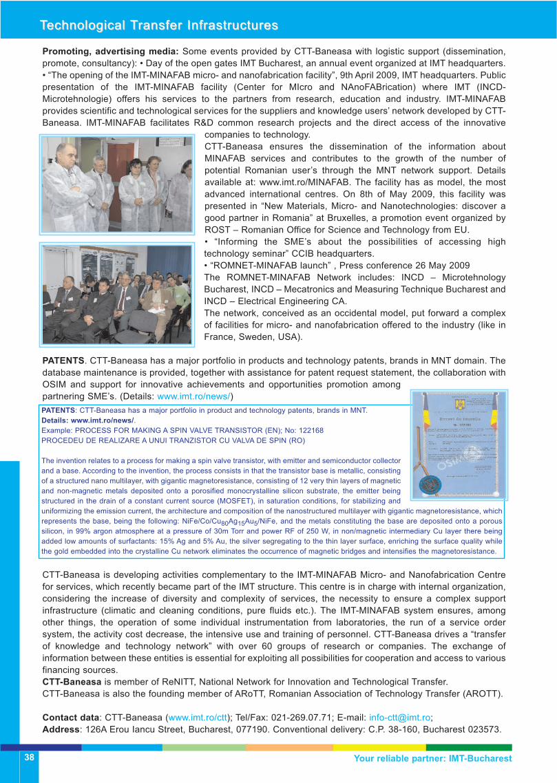
Promoting, advertising media: Some events provided by CTT-Baneasa with logistic support (dissemination,
promote, consultancy): • Day of the open gates IMT Bucharest, an annual event organized at IMT headquarters.
• “The opening of the IMT-MINAFAB micro- and nanofabrication facility”, 9th April 2009, IMT headquarters. Public
presentation of the IMT-MINAFAB facility (Center for MIcro and NAnoFABrication) where IMT (INCD-
Microtehnologie) offers his services to the partners from research, education and industry. IMT-MINAFAB
provides scientific and technological services for the suppliers and knowledge users’ network developed by CTT-
Baneasa. IMT-MINAFAB facilitates R&D common research projects and the direct access of the innovative
companies to technology.
CTT-Baneasa ensures the dissemination of the information about
MINAFAB services and contributes to the growth of the number of
potential Romanian user’s through the MNT network support. Details
available at: www.imt.ro/MINAFAB. The facility has as model, the most
advanced international centres. On 8th of May 2009, this facility was
presented in “New Materials, Micro- and Nanotechnologies: discover a
good partner in Romania” at Bruxelles, a promotion event organized by
ROST – Romanian Office for Science and Technology from EU.
• “Informing the SME’s about the possibilities of accessing high
technology seminar” CCIB headquarters.
• “ROMNET-MINAFAB launch” , Press conference 26 May 2009
The ROMNET-MINAFAB Network includes: INCD – Microtehnology
Bucharest, INCD – Mecatronics and Measuring Technique Bucharest and
INCD – Electrical Engineering CA.
The network, conceived as an occidental model, put forward a complex
of facilities for micro- and nanofabrication offered to the industry (like in
France, Sweden, USA).
PATENTS. CTT-Baneasa has a major portfolio in products and technology patents, brands in MNT domain. The
database maintenance is provided, together with assistance for patent request statement, the collaboration with
OSIM and support for innovative achievements and opportunities promotion among
partnering SME’s. (Details: www.imt.ro/news/)
CTT-Baneasa is developing activities complementary to the IMT-MINAFAB Micro- and Nanofabrication Centre
for services, which recently became part of the IMT structure. This centre is in charge with internal organization,
considering the increase of diversity and complexity of services, the necessity to ensure a complex support
infrastructure (climatic and cleaning conditions, pure fluids etc.). The IMT-MINAFAB system ensures, among
other things, the operation of some individual instrumentation from laboratories, the run of a service order
system, the activity cost decrease, the intensive use and training of personnel. CTT-Baneasa drives a “transfer
of knowledge and technology network” with over 60 groups of research or companies. The exchange of
information between these entities is essential for exploiting all possibilities for cooperation and access to various
financing sources.
CTT-Baneasa is member of ReNITT, National Network for Innovation and Technological Transfer.
CTT-Baneasa is also the founding member of ARoTT, Romanian Association of Technology Transfer (AROTT).
Contact data: CTT-Baneasa (www.imt.ro/ctt); Tel/Fax: 021-269.07.71; E-mail: [email protected];
Address: 126A Erou Iancu Street, Bucharest, 077190. Conventional delivery: C.P. 38-160, Bucharest 023573.
TTechnological echnological TTransfer Infrastructuresransfer Infrastructures
Your reliable partner: IMT-Bucharest38
PATENTS: CTT-Baneasa has a major portfolio in product and technology patents, brands in MNT.
Details: www.imt.ro/news/.
Example: PROCESS FOR MAKING A SPIN VALVE TRANSISTOR (EN); No: 122168
PROCEDEU DE REALIZARE A UNUI TRANZISTOR CU VALVA DE SPIN (RO)
The invention relates to a process for making a spin valve transistor, with emitter and semiconductor collector
and a base. According to the invention, the process consists in that the transistor base is metallic, consisting
of a structured nano multilayer, with gigantic magnetoresistance, consisting of 12 very thin layers of magnetic
and non-magnetic metals deposited onto a porosified monocrystalline silicon substrate, the emitter being
structured in the drain of a constant current source (MOSFET), in saturation conditions, for stabilizing and
uniformizing the emission current, the architecture and composition of the nanostructured multilayer with gigantic magnetoresistance, which
represents the base, being the following: NiFe/Co/Cu80Ag15Au5/NiFe, and the metals constituting the base are deposited onto a porous
silicon, in 99% argon atmosphere at a pressure of 30m Torr and power RF of 250 W, in non/magnetic intermediary Cu layer there being
added low amounts of surfactants: 15% Ag and 5% Au, the silver segregating to the thin layer surface, enriching the surface quality while
the gold embedded into the crystalline Cu network eliminates the occurrence of magnetic bridges and intensifies the magnetoresistance.

TTechnological echnological TTransfer Infrastructuresransfer Infrastructures
Your reliable partner: IMT-Bucharest
THE SCIENCE THE SCIENCE AND TECHNOLOGYAND TECHNOLOGY PPARK FOR ARK FOR MICRO MICRO AND NANOTECHNOLOGIES (MINAAND NANOTECHNOLOGIES (MINATECH-RO)TECH-RO)
The main objective of MINATECH-RO is to facilitate the access of the small companies to advanced technologies
(including start up companies/ incubation).
The Park was created in April 2004 and received institutional funding during 2004-2005 through the national
INFRATECH Program.
The specific objectives of MINATECH-RO:
• Technological transfer; • Designing of prototypes, demonstrators or experimental models;
• Small scale/pilot production after realizing (fabrication) the prototype; • Incubation;
• Technological services, micro-physical characterization, simulation and computer aided design;
• Learning/training by preparation of courses and stages (with practical training) in the Microsystems, micro- and
nanotechnologies and microengineering domains;
• Assistance and consultancy activities for SMEs and small innovative enterprises:
- Information in micro-engineering, Microsystems, micro- and nanotechnologies, access to databases,
documentation, etc; - Technological consultancy; - Brokerage (for the domain services); - Feasibility studies;
- Facilitating the access of Romanian innovative SMEs to European networks and partnerships;
• Dissemination of information (organizing conferences, workshops, editing publications, etc.);
• Research & Development;
Companies that activate in MINATECH-RO Park:
• S.C. ROM-QUARTZ S.A. (www.minatech.ro/romquartz) performs studies and scientific researches regarding
some BAW devices fabrication (bulk acoustic wave) and SAW (surface acoustic wave) based alternative
piezoelectric materials (lithium niobate, lithium tantalite langasite and gallium orthophosphate );
• S.C. SITEX 45 SRL (www.microsisteme.ro) manufactures 50 Pa – 100 kPa pressure sensors (rapid prototyping)
and ceramic capacitive transducers for low pressure, ceramic diaphragm and dedicated ASIC integrated circuits;
R&D activity: sensors, optoelectronic devices, transducers, pressure sensors, materials, MEMS; is offering
solutions regarding RFID identification: tags, cards;
• EUROPEAN BUSINESS INNOVATION & RESEARCH CENTER SA. R&D activity: micro/nanotechnology for
aeronautics and space applications, clean energy applications, precision agriculture applications, active
screening systems, protection against space residues and electromagnetic turbulences;
• S.C. ROMES S.A.
• OPTOTECH SRL–active electronic devices experience (photodiodes,
photothyristors, (photo)transistors;
• TELEMEDICA SA–R&D activity for bio applications;
• DDS DIAGNOSTIC SRL– produces other chemical reagents, R&D in physics and
natural science; Expertise: application research for in-vitro diagnostic medical
devices, design kits for in-vitro diagnostic, market studies for in-vitro diagnostic kits.
Research and industry interaction:
• Access to the MINATECH-RO incubator, scientific and technological park (IMT in
collaboration with UPB), park resident companies.
- Companies that collaborates with the consortium and/or offer services in park
have priority;
- Consultancy services are included;
• Access to scientific and technology services (local and abroad SMEs);
• Complex technologic assistance through CTT-Baneasa www.imt.ro/ctt;
Development of bio-Microsystems for genomic analysis (for health
and life quality development)– IMT collaboration with one of the parkresident companies (DDS DIAGNOSTIC): This experiment was possible
due to the new equipments: Omni Grid Micro Plotter and UC4
Scanner that are inside NanoBioLab from IMT Bucharest. These
equipments allow obtaining diagnostic chips, on glass or silicon, and
also, the results interpretation. This microarray chips obtained involve
multidisciplinary research in microtechnology, chemistry, biology,
physics and pharmacology.
39
Lavinia Ruta, pharmacist,
DDS DIAGNOSTIC
Monica Simion, and Teodora Ignat, in
NanoBioLab room, IMT-Bucharest

TTechnological echnological TTransfer Infrastructuresransfer Infrastructures
Your reliable partner: IMT-Bucharest
Research institutes cooperation:
• Access to new equipment, especially trough technologic networks that have laboratories inside IMT, so in
contact with the park. • Working point in technology area.
• Common scientific and technological services offer (park benefit in the first place)
• Possible strategic partnership with various domains institutes, in association with MINATECH-RO consortium.
Universities cooperation:
• Access in institute for masters and PhD students
• Common offer for education and training: Various partnership with
Romanian universities
• Contact points in universities: Partnership with Polytechnic University
of Bucharest
• Systematic cooperation (organize of a framework and a “interaction
space” in park): Possible “spin-off” from universities.
In park are located:
• Common laboratories for RO-NANOMED, NANOSCALE-CONV
and RTN-NANOEL networks. The laboratories are financed through
complex projects from CEEX program.
• National contact points for ENIAC, NANOMEDICINE, PHOTONICS 21 European technological platforms.
• Contact points for German networks (IVAM, NANOBIONET and MST Network Rhein Main) and for Romanian-
German Micro- and Nanotechnologies Centre.
The Science and Technology Park for Micro and Nanotechnologies MINATECH-RO (www.minatech.ro) was
established using the resources offered by the IMT-Bucharest (www.imt.ro ) and the “Politehnica” University of
Bucharest (PUB) in a national consortium that created the park (opened in June 2006). The Park is
administrated by SC MINATECH ADMINISTRATOR SRL.
MINATECH-RO is participating to technological transfer dedicated actions (informing, exhibitions, innovation
road show, debate-seminars in this domain). At the Research Salon 2008, the resident companies, their
competence and offer were promoted. The opportunity to meet the interest people and establish partnerships
was offered for the company representatives. The first edition of the Research Excellency Top has brought the
first place and a gold medal for MINATECH-RO - Scientific and Technologic Park for Micro and
Nanotechnologies, which IMT-Bucharest and UPB (“Politechnica” University of Bucharest) are part of. A first
place at the section “Innovative SME” from the Research Excellency Top was offered to SC SITEX 45 SRL, a
resident company in MINATECH-RO Park.
Interactions in infrastructures developed by IMT-Bucharest:
Access to technological and characterization services for the partners from research, education and industry are
available through IMT-MINAFAB, Micro- and Nanofabrication Centre (IMT-Centre for Micro- and
NAnoFABrication), where IMT (National Institute for R&D in Microtechnologies) offers services for partners from
research, education and industry domain. Details: www.imt.ro/MINAFAB.
A part of the MINATECH-RO specific objectives, linked to the technology transfer and services providing
(including training and consultancy), is implemented through CTT-Baneasa, a TTI entity that autonomous acts
inside IMT. CTT-Baneasa provides services (consultancy, dissemination etc.) for Park companies, and facilitates
access to the services offered by IMT. These companies can contribute to the diversification of the IMT technical
services offer.
Estimated benefits for the potential beneficiary: The companies, that have direct benefits from the facilities
offered by the Park and the coordinator consortium also, have access to the state-of-the-art technology for
micro- and nanofabrication, characterization techniques, simulation, modelling and computer aided design. The
companies can install equipments in technology area and can develop microproduction activities. The access to
high-tech offers to innovative SMEs the advantage to create competitive products and also, the possibility to
successfully access the public funds designated for RDI. By cooperating with the Park, the companies will have
easy access to set up national and international partnerships.
Contact data: MINATECH-RO (www.minatech.ro); Tel: 021-269.07.67; E-mail: [email protected];
Address: 126 A Erou Iancu Street, Bucharest, 077190. Conventional delivery: C.P. 38-160, Bucharest 023573.
40

Networking, ITNetworking, IT services, Publishingservices, Publishing
Your reliable partner: IMT-Bucharest
Electronic dissemination and networkingElectronic dissemination and networking
�� Inventory and Networking of researchers and research centers (research institutes, organization,
SME) for active participation in FP 6, FP7 and European technological platforms. The networking focused on
interaction between researchers active in micro-nano-bio technologies field at European level based on previous
experience gained in MINOS-EURONET (http://www.minos-euro.net), MINAEAST (http://www.minaeast.net).
IMT-Bucharest is active in: • European Technology Platform for Micro- and NanoManufacturing (MINAM);
• European technology platforms ENIAC; • PHOTONICS21;
• Future Manufacturing Technologies MANUFUTURE;
�� Dissemination of information about the researchers, centres, institutes expertise, research interest,
involvement in international projects trough e-newsletter, electronic and printed MNT Bulletin, flyers, and
posters.
Communication with partners; dissemination of information about institute and institute partners, research
activities, national and international projects; develop and maintain the internet “interface” regarding all activities
carried on by the institute; administration and maintenance of specially designed communication platform for
networking.
�� IT services: • IT services: interactive databases, web pages on Internet, Intranet, Extranet, specially
designed e-room communication platform for networking.
• INTERNET & INTRANET applications design, web sites design and maintenance;
• Interactive database design and application, creation and maintenance;
• Soft and hard integration of designed system;
• IT maintenance, system development; Consulting in IT problems and development;
• Equipment up-grade, maintenance and PC network internal organization;
• Administration of communication platform for networking (web-based application that allows gradual access to
a virtual space, reducing costs for project management and enhancing transparency of communication. General
functionalities: offers a user rights system and a file management policy and capabilities to describe projects by
publishing web media content.)
IT and communication infrastructure: 100Mb/s computer network (IBM servers, CISCO routers), radio and
optical fibre connection to Internet, 2 computer networks for courses, training and conferences (one connected
to the graphic station Dual IBM 3750 Server with 8 quad-core Intel Xeon MP 2.93 GHz processors, 196 GByte
RAM and 1 TByte HDD+876 GByte external storage)
�� Editing and publishing:• Series of books in Micro and Nanoengineering (since 2001) published by the Romanian Academy.(Last
volume No. 15) ”New Developments in Micro Electro Mechanical Systems for Radio Frequency and Millimeter
Wave Applications”, Editors: George Konstantinidis, Alexandru Muller, Dan Dascalu, Robert Plana. Web:
http://www.nano-link.net/mne
• Romanian Journal for Information Science and Technology (of the Romanian Academy), quoted in the
Thomson ISI database; Web: http://www.imt.ro/romjist
• International publications in English (editing): Micro and Nanotechnologies (MNT) Bulletin (since 2000, MNT
activities in Romania; since 2004 MNT activities in Eastern Europe), also on http://www.imt.ro/MNT;
�� Organizing scientific conferences and other events:• International conferences: CAS Conference, IEEE annual event (in 2009 at its 32nd edition); Web:
http://www.imt.ro/cas
• International events such as Micromechanics Europe (in 2002), MEMSWAVE (first two editions), the first
Nanoforum Workshop (2003).
• National Seminar of Nanoscience and Nanotechnology (annually edition since 2004). Web:
http://www.romnet.net
41

IMTIMT-Bucharest participation to FP7 projects-Bucharest participation to FP7 projects
Directors:Directors:
General Manager (CEO) an President of the Board: Prof. Dan DASCALU ([email protected])
Scientific Director: Dr. Raluca MULLER ([email protected])
Technical Director: Dr. Nicolae MARIN ([email protected])
Economic Director: Domnica Geambazi ([email protected])
Director of Research Centre for Integration of Technologies: Dr. Mircea DRAGOMAN
Director of Centre for Scientific Services: Dr. Radu Cristian POPA ([email protected])
President of the Scientific Council: Dr. Alexandru Muller ([email protected])

With the occasion of the Info and brokerage event: “Micro- and nanosystems in the FP7/2007 call”, Bucharest, Romania, 24
May 2007, Augusto de Albuquerque, Head of Unit, INFSO G.2 Microsystems, EC, visited IMT-Bucharest.
The main point of the visit was IMT-Bucharest technology area, which allows
structures manufacturing at the micrometer or nanometer scale. The new equipments
acquired during the last years were presented. Some of the laboratories such as Microand Nano-Photonics, Simulation Modelling and Computer Aided Design lab and
Micromachined structures, microwave circuits and devices lab have been visited also.
After the visit, Augusto de Albuquerque wrote down the following remarks in the
institute Guest Book:
“I enjoyed very much to see the very good infrastructure and the organization to build the full chain: simulation, design, testing and manufacturing. Congratulations for the very systematic building of competence in MEMS, Photonics and Nano-Bio convergence. Best wishes for the future.
Augusto de Albuquerque, Head of Unit Microsystems, EC-DG InformationSociety and Media”
European Commission officials visiting IMT-Bucharest
With the occasion of the Info- and brokerage event in new technologies and materials (FP7/2007: NMP/ICT) “Cooperation in
industry-oriented research in an enlarged Europe”, Bucharest, Romania, on 22-23 March 2007, Dirk Beernaert, Head ofunit “Nanoelectronics”, DG Information Society and Media, EC and Nicholas Hartley, Acting Director “Industrial technologies”,DG Research, EC visited IMT-Bucharest and wrote down the following remarks in the institute Guest Book:
“I very much enjoyed the visit of the Institute and the Conference. IMT is doinginteresting work. The work is also important for future long term applications and for innovation in the nanotechnology, bio-nanotechnology field andfor nanophotonics. I hope they get fast the right equipment to play on important roleon the European scene.
In the Conference, I have very much appreciated that they form a good focal point forthe local and for the participants from the NMS. This is very much appreciated…
Dirk Beernaert, DG-IST, Head of UnitNanoelectronics”
“A very impressive centre with a good team during interesting and importantwith. I have very much enjoyed this visit. Thank you for your excellent hospitality– good luck for the future and keep up the good work.
Nicholas Hartley”

126A, Erou Iancu Nicolae Street, R-077190
Mailing address: PO-BOX 38-160, 023573,
Bucharest, ROMANIATel: +40-21-269.07.74; +40-21-269.07.70
Fax: +40-021-269.07.72; +40-021-269.07.76
National Institute for R&D in MicrotechnologiesNational Institute for R&D in Microtechnologies
http://www.imt.ro
IMT-Bucharest is publishing scientific report annually since 2005.The annual reports are available at http://www.imt.ro
Piata presei libere
Victoria Square
Universitate Square
Unirea Square
IMTIMT-MINAF-MINAFAB AB http://www.imt.ro/MINAFAB


![SAFEAIR 2014IMT.ppt [Read-Only] · Coordinating organization: National R&D Institute for Microtechnology, IMT-Bucharest Status: organization of public interest, autonomous, coordinated](https://img.pdfslide.us/doc/110x75/5f3f9c1224d91016325e3f64/safeair-read-only-coordinating-organization-national-rd-institute-for-microtechnology.jpg)