Embed Size (px)
Citation preview
CYCLE TIME ANALYSIS FOR PHOTOLITHOGRAPHY TOOLS IN
SEMICONDUCTOR MANUFACTURING INDUSTRY WITH SIMULATION
MODEL: A CASE STUDY
by
SIOW YUEN TIEN
Thesis submitted in fulfillment of the
requirements for the degree
of Master of Science
November 2008

ii
ACKNOWLEDGEMENTS
First and foremost, I would like to express my special thanks to Dr. Shahrul
Kamaruddin, from school of mechanical engineering (University Sains Malaysia)
who has given all the support towards the accomplishment of this research. I would
like to express my sincere thanks to him for his invaluable advice and guidance
throughout the entire duration for completion of this research.
I would like to thank my family for their love and moral support, which gave
me the strength to complete this research successfully. Added to that, I would also
like to thank all my friends and people who had helped me directly or indirectly in
completing this research.
Last but not least, this research was conducted at Silterra Malaysia wafer
fabrication facility. I wish to gratefully acknowledge the members of Industrial
Engineering department in Silterra for their dedicated help and support throughout
the study and their useful insights. Without the strong management support and
commitment from all engineers and manager involved, simulation as a powerful
management tool would not be successful.
Y.T. Siow
November 2008
iii
TABLE OF CONTENTS
Page
ACKNOWLEDGEMENTS ii
TABLE OF CONTENTS iii
LIST OF TABLES vi
LIST OF FIGURES vii
LIST OF ABBREVIATIONS ix
LIST OF APPENDICES x
LIST OF PUBLICATIONS xi
ABSTRAK xii
ABSTRACT xiii
CHAPTER ONE - INTRODUCTION
1.0 Overview 1
1.1 Problem Statement 3
1.2 Objectives 3
1.3 Proposed Methodology 3
1.4 Thesis Outline 4
CHAPTER TWO - LITERATURE REVIEW
2.0 Overview 5
2.1 Mathematical Approach 5
iv
2.2 Dispatching Rules 10
2.3 Simulation Model 18
2.4 Summary 27
CHAPTER THREE - METHODOLOGY
3.0 Overview 29
3.1 Photolithography Process 29
3.2 Simulation Study 33
3.3 Phase 1 34
3.3.1 Problem Identification 35
3.3.2 Setting Objectives of Simulation Model 35
3.3.3 Conceptual Model 36
3.4 Phase 2 38
3.4.1 Model Verification and Validation 38
3.5 Phase 3 40
3.5.1 Model Experimentation 40
3.5.2 Methods in Results Analysis 44
3.5.2.1 Test of Significance 45
3.6 Summary 47
CHAPTER FOUR - EXPERIMENT
4.0 Overview 48
4.1 Description of Simulation Software 48
4.2 IDEF0 of Photolithography 52
4.3 Photolithography Simulation Model 59
v
4.3.1 Photolithography Model Verification and Validation 62
4.4 Experimental Design 67
4.4.1 Experiment 1 67
4.4.2 Experiment 2 74
4.5 Summary 77
CHAPTER FIVE - RESULTS AND DISCUSSION
5.0 Overview 78
5.1 Results for Experiment 1 78
5.2 Results for Experiment 2 84
5.3 Further Analysis 94
5.4 Summary 104
CHAPTER SIX - CONCLUSION
6.0 Overview 105
6.1 Future Work 106
REFERENCES 107
APPENDICES
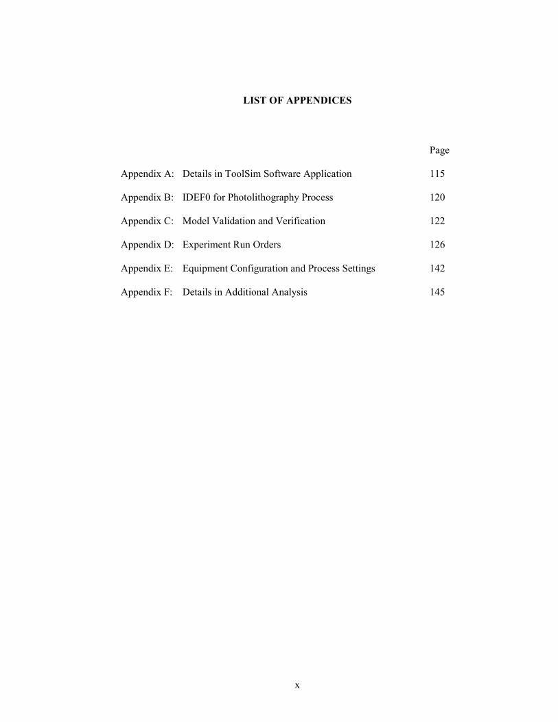
Appendix A: Details in ToolSim Software Application 115
Appendix B: IDEF0 for Photolithography Process 120
Appendix C: Model Validation and Verification 122
Appendix D: Experiment Run Orders 126
Appendix E: Equipment Configuration and Process Settings 142
Appendix F: Details in Additional Analysis 145
vi
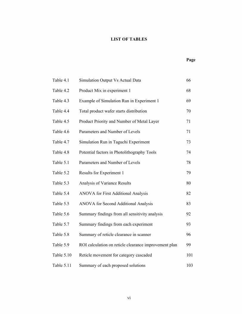
LIST OF TABLES
Page
Table 4.1 Simulation Output Vs Actual Data 66
Table 4.2 Product Mix in experiment 1 68
Table 4.3 Example of Simulation Run in Experiment 1 69
Table 4.4 Total product wafer starts distribution 70
Table 4.5 Product Priority and Number of Metal Layer 71
Table 4.6 Parameters and Number of Levels 71
Table 4.7 Simulation Run in Taguchi Experiment 73
Table 4.8 Potential factors in Photolithography Tools 74
Table 5.1 Parameters and Number of Levels 78
Table 5.2 Results for Experiment 1 79
Table 5.3 Analysis of Variance Results 80
Table 5.4 ANOVA for First Additional Analysis 82
Table 5.5 ANOVA for Second Additional Analysis 83
Table 5.6 Summary findings from all sensitivity analysis 92
Table 5.7 Summary findings from each experiment 93
Table 5.8 Summary of reticle clearance in scanner 96
Table 5.9 ROI calculation on reticle clearance improvement plan 99
Table 5.10 Reticle movement for category cascaded 101
Table 5.11 Summary of each proposed solutions 103
vii
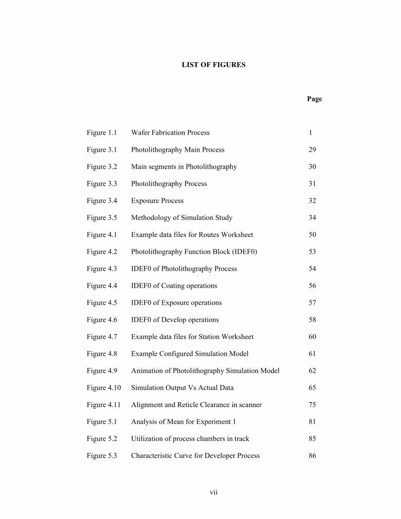
LIST OF FIGURES
Page
Figure 1.1 Wafer Fabrication Process 1
Figure 3.1 Photolithography Main Process 29
Figure 3.2 Main segments in Photolithography 30
Figure 3.3 Photolithography Process 31
Figure 3.4 Exposure Process 32
Figure 3.5 Methodology of Simulation Study 34
Figure 4.1 Example data files for Routes Worksheet 50
Figure 4.2 Photolithography Function Block (IDEF0) 53
Figure 4.3 IDEF0 of Photolithography Process 54
Figure 4.4 IDEF0 of Coating operations 56
Figure 4.5 IDEF0 of Exposure operations 57
Figure 4.6 IDEF0 of Develop operations 58
Figure 4.7 Example data files for Station Worksheet 60
Figure 4.8 Example Configured Simulation Model 61
Figure 4.9 Animation of Photolithography Simulation Model 62
Figure 4.10 Simulation Output Vs Actual Data 65
Figure 4.11 Alignment and Reticle Clearance in scanner 75
Figure 5.1 Analysis of Mean for Experiment 1 81
Figure 5.2 Utilization of process chambers in track 85
Figure 5.3 Characteristic Curve for Developer Process 86
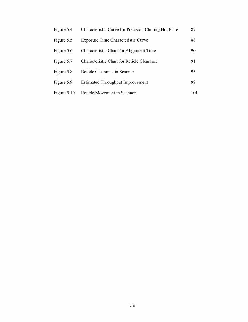
viii
Figure 5.4 Characteristic Curve for Precision Chilling Hot Plate 87
Figure 5.5 Exposure Time Characteristic Curve 88
Figure 5.6 Characteristic Chart for Alignment Time 90
Figure 5.7 Characteristic Chart for Reticle Clearance 91
Figure 5.8 Reticle Clearance in Scanner 95
Figure 5.9 Estimated Throughput Improvement 98
Figure 5.10 Reticle Movement in Scanner 101
ix
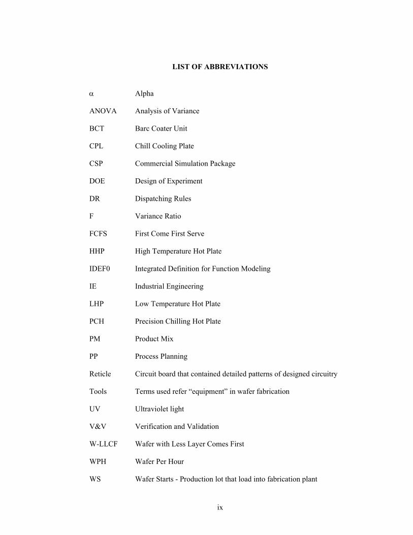
LIST OF ABBREVIATIONS
α Alpha
ANOVA Analysis of Variance
BCT Barc Coater Unit
CPL Chill Cooling Plate
CSP Commercial Simulation Package
DOE Design of Experiment
DR Dispatching Rules
F Variance Ratio
FCFS First Come First Serve
HHP High Temperature Hot Plate
IDEF0 Integrated Definition for Function Modeling
IE Industrial Engineering
LHP Low Temperature Hot Plate
PCH Precision Chilling Hot Plate
PM Product Mix
PP Process Planning
Reticle Circuit board that contained detailed patterns of designed circuitry
Tools Terms used refer “equipment” in wafer fabrication
UV Ultraviolet light
V&V Verification and Validation
W-LLCF Wafer with Less Layer Comes First
WPH Wafer Per Hour
WS Wafer Starts - Production lot that load into fabrication plant
x
LIST OF APPENDICES
Page
Appendix A: Details in ToolSim Software Application 115
Appendix B: IDEF0 for Photolithography Process 120
Appendix C: Model Validation and Verification 122
Appendix D: Experiment Run Orders 126
Appendix E: Equipment Configuration and Process Settings 142
Appendix F: Details in Additional Analysis 145
xi
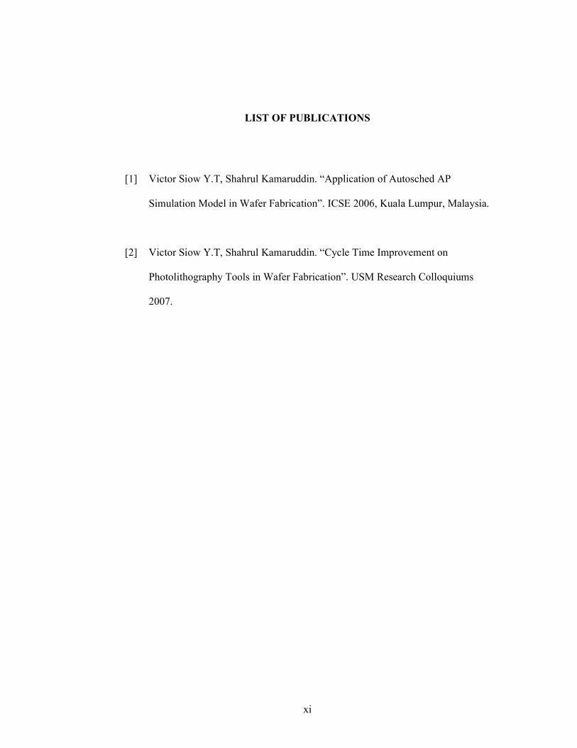
LIST OF PUBLICATIONS
[1] Victor Siow Y.T, Shahrul Kamaruddin. “Application of Autosched AP
Simulation Model in Wafer Fabrication”. ICSE 2006, Kuala Lumpur, Malaysia.
[2] Victor Siow Y.T, Shahrul Kamaruddin. “Cycle Time Improvement on
Photolithography Tools in Wafer Fabrication”. USM Research Colloquiums
2007.
xii
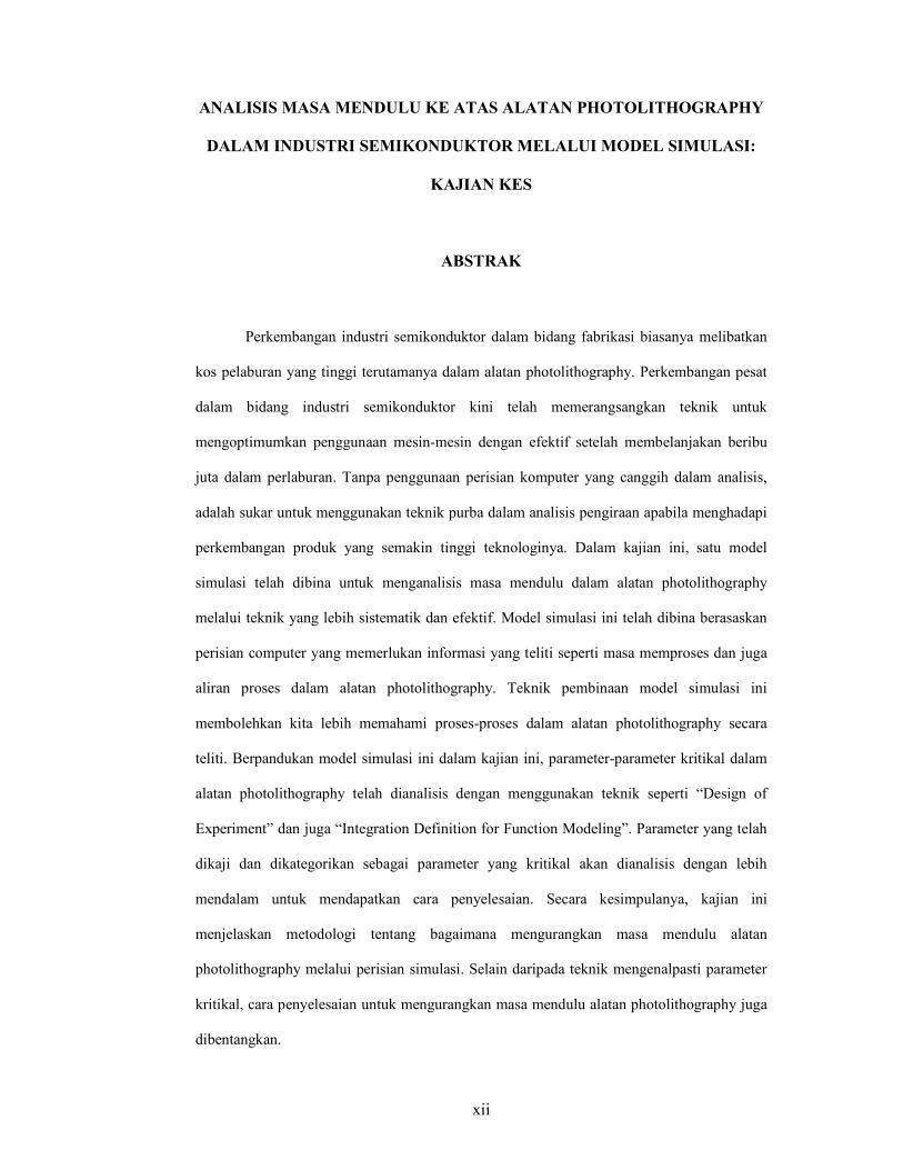
ANALISIS MASA MENDULU KE ATAS ALATAN PHOTOLITHOGRAPHY
DALAM INDUSTRI SEMIKONDUKTOR MELALUI MODEL SIMULASI:
KAJIAN KES
ABSTRAK
Perkembangan industri semikonduktor dalam bidang fabrikasi biasanya melibatkan
kos pelaburan yang tinggi terutamanya dalam alatan photolithography. Perkembangan pesat
dalam bidang industri semikonduktor kini telah memerangsangkan teknik untuk
mengoptimumkan penggunaan mesin-mesin dengan efektif setelah membelanjakan beribu
juta dalam perlaburan. Tanpa penggunaan perisian komputer yang canggih dalam analisis,
adalah sukar untuk menggunakan teknik purba dalam analisis pengiraan apabila menghadapi
perkembangan produk yang semakin tinggi teknologinya. Dalam kajian ini, satu model
simulasi telah dibina untuk menganalisis masa mendulu dalam alatan photolithography
melalui teknik yang lebih sistematik dan efektif. Model simulasi ini telah dibina berasaskan
perisian computer yang memerlukan informasi yang teliti seperti masa memproses dan juga
aliran proses dalam alatan photolithography. Teknik pembinaan model simulasi ini
membolehkan kita lebih memahami proses-proses dalam alatan photolithography secara
teliti. Berpandukan model simulasi ini dalam kajian ini, parameter-parameter kritikal dalam
alatan photolithography telah dianalisis dengan menggunakan teknik seperti “Design of
Experiment” dan juga “Integration Definition for Function Modeling”. Parameter yang telah
dikaji dan dikategorikan sebagai parameter yang kritikal akan dianalisis dengan lebih
mendalam untuk mendapatkan cara penyelesaian. Secara kesimpulanya, kajian ini
menjelaskan metodologi tentang bagaimana mengurangkan masa mendulu alatan
photolithography melalui perisian simulasi. Selain daripada teknik mengenalpasti parameter
kritikal, cara penyelesaian untuk mengurangkan masa mendulu alatan photolithography juga
dibentangkan.
xiii
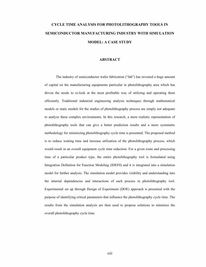
CYCLE TIME ANALYSIS FOR PHOTOLITHOGRAPHY TOOLS IN
SEMICONDUCTOR MANUFACTURING INDUSTRY WITH SIMULATION
MODEL: A CASE STUDY
ABSTRACT
The industry of semiconductor wafer fabrication (“fab”) has invested a huge amount
of capital on the manufacturing equipments particular in photolithography area which has
driven the needs to re-look at the most profitable way of utilizing and operating them
efficiently. Traditional industrial engineering analysis techniques through mathematical
models or static models for the studies of photolithography process are simply not adequate
to analyze these complex environments. In this research, a more realistic representation of
photolithography tools that can give a better prediction results and a more systematic
methodology for minimizing photolithography cycle time is presented. The proposed method
is to reduce waiting time and increase utilization of the photolithography process, which
would result in an overall equipment cycle time reduction. For a given route and processing
time of a particular product type, the entire photolithography tool is formulated using
Integration Definition for Function Modeling (IDEF0) and it is integrated into a simulation
model for further analysis. The simulation model provides visibility and understanding into
the internal dependencies and interactions of each process in photolithography tool.
Experimental set up through Design of Experiment (DOE) approach is presented with the
purpose of identifying critical parameters that influence the photolithography cycle time. The
results from the simulation analysis are then used to propose solutions to minimize the
overall photolithography cycle time.
1
CHAPTER ONE
INTRODUCTION
1.0 Overview
Semiconductor wafer fabrication or “fab” is one of the most complex
manufacturing processes found today. In today’s global business environment, it
requires most of the companies to adapt new technologies in order to stay
competitive. Wafers is the term used in the manufacturing of semiconductor devices
and integrated circuits, depending on the material wafer diameter ranging from 25
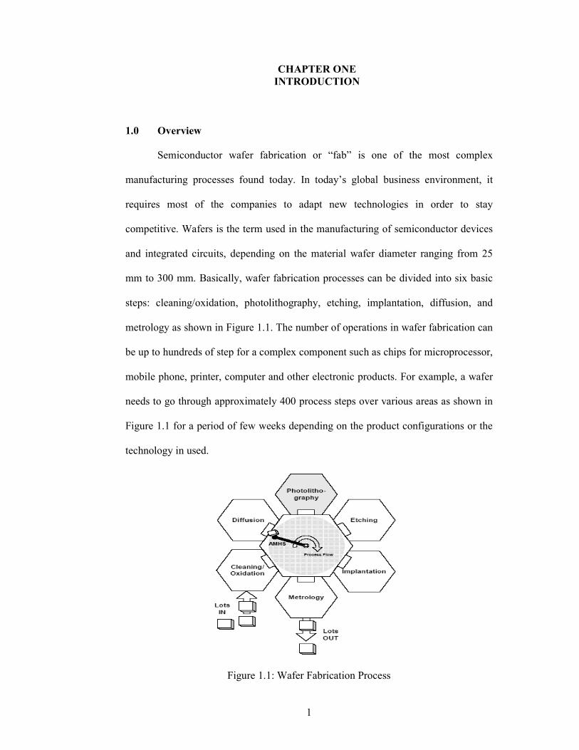
mm to 300 mm. Basically, wafer fabrication processes can be divided into six basic
steps: cleaning/oxidation, photolithography, etching, implantation, diffusion, and
metrology as shown in Figure 1.1. The number of operations in wafer fabrication can
be up to hundreds of step for a complex component such as chips for microprocessor,
mobile phone, printer, computer and other electronic products. For example, a wafer
needs to go through approximately 400 process steps over various areas as shown in
Figure 1.1 for a period of few weeks depending on the product configurations or the
technology in used.
Figure 1.1: Wafer Fabrication Process
2
In wafer fabrication, cycle time is the length of time from where the bare
silicon wafers start to the final metrology test. Cycle time consists of queuing time
for the equipment, waiting time due to preventive maintenance, breakdown or
engineering hold, processing time, inspection time, and transportation time. Wafer
manufacturers strive to reduce the cycle time by simplifying the process and design
by improving the production control mechanisms for effective scheduling, better
dispatching, reliability, improving the layout for effective material handling, and
batch size changes to reduce queuing times or to decrease setups which are some of
the measures taken. By having a shorter cycle time, a manufacturer can fulfill the
customer’s orders more quickly and be more responsive to the market. Furthermore,
as the cycle time gets shorter, problems in the process can be diagnosed quicker,
allowing for faster process development and refinement. Hence, wafer manufacturers
exercise strict control over the cycle time and make continuous efforts in reducing it
to remain competitive.
In wafer fabrication, photolithography area is usually the bottleneck process
with the most expensive equipment in the production line. Being one of the processes
that is repeated the most during fabrication, any reduction in photolithography cycle
time will reduce the overall wafer fabrication cycle time. In this way it is assumed
that photolithography is the central process in the manufacturing plant and each
wafers has to pass through the process multiple times prior the completion of the
whole fabrication process. In addition, Photolithography is also considered as the
most complex operation in wafer fabrication that requires great precision. It is a
process that is used to create multiple layers of circuit patterns on a chip. During
photolithography process, the circuit patterns are transferred from a mask onto the
3
photosensitive polymer and finally the pattern is replicated in the underlying layer of
the wafer surface. Details of photolithography process will be further explained in
Chapter 3.
1.1 Problem Statement
With the vast amount of capital invested in the photolithography tools,
finding hidden capacity and improving cycle time of photolithography tool is a
common goal in wafer fabrication to increase overall throughput. Being one of the
processes that is considered bottleneck and repeated the most during fabrication, any
improvement in photolithography area will improve overall fab throughput as well.
The tools in the photolithography process are extremely expensive and thus, the risk
to perform experimentation within the real systems is very high. Hence the
motivation behind this research is to study a method that will effectively minimize
the photolithography cycle time.
1.2 Objectives
• To identify potential area in photolithography tool for cycle time
improvement.
• To conduct further analysis and evaluate the impact of potential factors to
process performance.
1.3 Proposed Methodology
The proposed method is to reduce waiting time and increase utilization of the
critical photolithography process area, which would result in an overall cycle time
reduction. For a given route and processing time of a particular product type, the
entire photolithography cell is formulated using Integration Definition for Function
4
Modeling (IDEF0) and it is integrated into a simulation model for further analysis.
The experimental set up through Design of Experiment (DOE) approach is presented
with the purpose of identifying critical parameters that influence the
photolithography cycle time. The results from the simulation analysis are used to
propose solutions to minimize the photolithography cycle time.
1.4 Thesis Outline
This thesis is organized and divided into six different chapters. Chapter 1 is
an introduction chapter. This chapter introduced the overview of wafer fabrication
process, problem statement, objectives of the project and the description of the
outline of the research. Chapter 2 is the literature review of the research. This chapter
discussed most of the relevant methods done by other researchers to improve cycle
time and increased overall machine throughput in semiconductor manufacturing.
Relevant case studies and proposed methodologies to improve photolithography area
are also discussed. Chapter 3 described the methodology of this research to meet
defined objectives. The steps and methods involved in meeting objectives are
explained. Methodology to conduct experiments and methods to evaluate
performance measure are discussed. Chapter 4 described in details the method used
to build a valid model using conceptual modeling and the integration of simulation
model to run experiments. The ways of building a model, setting up experiments and
running simulation models are also included in this chapter. Chapter 5 discussed the
analysis of simulation results and the discussion for proposed case studies. Results
are analyzed by using standard statistical method and also discussed the findings
from each experiment. Improvement plans are proposed and Chapter 6 summarized
the overall research and also the directions for future research.
5
CHAPTER TWO
LITERATURE REVIEW
2.0 Overview
This research shows the complexity of photolithography process in wafer
fabrication. The aim behind this research is to show that photolithography tools are
extremely expensive and thus, optimizing the performance of photolithography tools
is one of the significant goals to achieve cost saving. Therefore, this chapter reviewed
the previous case studies that had successfully proposed various types of
methodology to perform improvement plans on processing tools in the industry of
wafer fabrication. The literature review includes work reported regarding the
methods in cycle time improvement especially in wafer fabrication facility and,
particularly, the photolithography processing area. The review will focused on the
following types of approaches.
2.1 Mathematical Approach
In semiconductor manufacturing, mathematical approach is usually used to
obtain optimal solution in various types of complex manufacturing system. The
followings described the examples of reported work on mathematical approaches to
improve cycle time and increase throughput in the manufacturing environment.
Kurt and Murray (1996) presented nonlinear programming methods for
capacity planning in a semiconductor manufacturing system that consists of a set of
machines or workstations producing multiple products. The facility was modeled as
an open network of queues where capacity at each workstation in the system may be
changed dynamically for a certain period of time. To determine the timing and size of
6
the capacity changes, the authors presented two nonlinear programming models and
methods for solving the budget constraints on capacity costs. One model involves
minimizing the total capacity costs such that plant congestion is controlled via upper
limits on work-in-process. The other model involves minimizing a weighted sum of
product cycle time subject to budget constraints on capacity costs. As a result, both
presented models had been implemented as the optimization framework that guides
the timing and size of capacity changes where it allows performance measures such
as capacity costs, work-in-process, and product lead times to be controlled.
Mansour and Saeid (2003) addressed the problems of part loading, tool
loading, and part scheduling in flexible manufacturing systems. The authors
developed a mathematical model through integer programming to select machines
and assign operations and the required tools. The objective is to minimize the
summation of maximum completion time, material handling time, and the total
processing time. The authors assumed that there is a set of tools with known life and
a set of machines that can produce a variety of parts. A batch of various part types is
routed through this system with the assumption that the processing time and cost vary
with the assignment of parts to different machines and assignment of various toolsets
to machines. The results reported in the paper demonstrated the model efficiency in
the performance of the system with respect to measure such as production rate and
utilization. In a related study, Bulent et al (2003) presented a mathematical model for
the multi-period tool capacity planning in semiconductor manufacturing. The author
implemented the same approach where an integer programming model is developed
to minimize the machine tool operating costs, new tool acquisition costs, and
inventory holding costs.
7
Kao et al (2005) presented a mathematical model based on the theory of
constraints (TOC) concept. The objective is to improve product cycle time and
increase overall photolithography throughput by identifying and correcting
bottlenecks in the flow of wafers through multiple, associative segments of the
photolithography equipment. In the study, segmental rather than total processing
times is monitored in order to identify the segments which have the longest
processing times. The throughput is calculated by dividing the total segment process
time by the number of process chambers in the corresponding segment. The authors
managed to identify the process segment that represented a bottleneck in the
photolithography process, and made improvements on bottleneck segment that
resulted in a greater throughput increment.
Vladimir et al (2006) solved the single-robot cyclic scheduling problem
through linear programming. With a fixed robot operation sequence and time
window constraints on processing times, it generalizes the known single-part fixed-
sequence problems into a processing network with multiple part types and setup time
requirements. As a result, the author managed to prove that the problem is equivalent
to the parametric critical path problem, and proposed a polynomial time solution
algorithm that uses a new labeling procedure to identify all feasible parameter values.
Chen et al (2006) proposed a mathematical programming approach to
construct the membership function of the performance measure of the machine
interference system. Machine interference is an important problem frequently
encountered in manufacturing operations such as semiconductor manufacturing. Due
8
to uncontrollable factors, parameters in the machine interference problem may lead to
the machine breakdown rate and the service rate. The lower and upper bounds of the
fuzzy performance measure are calculated via a pair of mathematical programs for
different values of confidence interval. Data are adopted to construct the
corresponding membership function. As a result, the authors successfully
demonstrated the validity of the proposed approach and managed to obtain more
information for designing machine interference systems.
Wu and Chien (2007) developed a mathematical programming model to
optimize the scheduling in the final test area of semiconductor manufacturing. The
study provided an algorithm to specify the machine configuration of each job and
allocate specific resources in the final test area. The authors said the overall flow of
the final test of integrated circuits (IC) can be represented by the job shop model with
limited simultaneous multiple resources. Various product mixes, jobs recirculation,
uncertain arrival of jobs and unstable processing times are some of the factors that
will complicate the scheduling problem. In the study, the proposed approach
managed to increase productivity performance through a detail scheduling method
that can be graphically represented as timetables for the final test area.
Wang et al (2007) developed a simultaneous resource portfolio decision
model as a non-linear integer programming. The authors proposed a genetic
algorithm to maximize their profits by developing a proper resource portfolio plan
for simultaneously deploying resources and selecting the most profitable orders.
Various important factors, such as resource investment alternatives, trade-offs
between the price and speed of equipment and capital time value had increased the
9
complexity of the simultaneous resource portfolio problem. Thus, the proposed
method is employed in the context of semiconductor testing industry to support
decisions regarding equipment investment alternatives (including new equipment
procurement, rent and transfer by outsourcing, and phasing outing) for simultaneous
resources (such as testers and handlers) and task allocation. As a result, the proposed
method had played an important role in decision-making regarding equipment
investment and indirectly helps in minimizing the overall product cycle time.
Fuh et al (2007) proposed a mixed integer-programming model to solve
dynamic scheduling problem of semiconductor burn-in operations. The study is
aimed to minimize the total completion time subjected to deadline constraints. The
burn-in oven is a batch-processing machine and the size of each job is independent of
the oven’s capacity. Computational experiments indicated that the proposed model
could effectively and efficiently obtain optimal solutions for small size problems and
also provide high-quality solutions for large size problems.
On the other hand, Na Li et al (2007) developed a graph decision aid for
single-station semiconductor manufacturing systems. The relationships between key
indicators of manufacturing system performance, such as cycle time, throughput,
utilization, work-in-process, and the variability factor, are complicated and difficult
to quantify. In most cases, manufacturing managers cannot optimize one
characteristic without adversely affecting another. For example, in order to reduce
inventory and minimize time-to-market, one may need to lower the WIP level to
reduce cycle time; however, too much WIP reduction can lead to unexpected station
starvation (stoppage) and, thus, degrade throughput. Low utilization of expensive
10
equipment is also unacceptable, especially for advanced semiconductor
manufacturing. Consequently, the authors had developed a regression model with
simple ‘‘what-if’’ analyses and assist with the forecast of future influencing factors,
thus permitting quicker decisions making.
In semiconductor industry, wafer manufacturers must be precise on tool
elimination due to changes caused by demand, product mixes, and overseas fab
capacity expansion. Chung and Hsieh (2007) proposed a mechanism for tool
portfolio elimination that determines which equipment can be eliminated in wafer
fabrication. The authors developed an integer-programming model to avoid trial-and-
error and to obtain the optimal solution in decision-making. In the proposed
mechanism, product mix, wafer output, capital expenditure, tool utilization,
protective capacity, and cycle time are considered seriously in the overall evaluation.
The results showed that the proposed mechanism can effectively identify the correct
tools for elimination with a large capital savings with little cycle time impact.
2.2 Dispatching Rules
The dispatching rules (DR) are one of the most widely used methods to
schedule the wafer manufacturing process. They are applied to select which job to
process next on a particular process tool. The use of the DR is often motivated by the
fact that they are fast and simple to implement in the dynamic manufacturing
environment especially in the semiconductor industry. Various works have been
carried out that emphasized on the dispatching rules. The followings are some of the
related works.
11
Elif Akcali et al (2000) examined the effects of different loading and
dispatching policies for diffusion operations in a wafer fabrication facility. In wafer
fabrication, furnace refers to batch processing machine for diffusion operations,
which can simultaneously process a small amount of production lots together as a
batch. Whenever a furnace becomes available, scheduling the next batch involves
decisions on both which operation to schedule next (dispatching policy) and how
many lots to put into each of a batch (loading policy). The author conducted three
sets of experiments. The first experiment aimed towards finding the optimal loading
policy for the system. The second experiment is a sensitivity analysis to study
different dispatching policies such as lot with the lowest critical ratio (LLCR), first-
come-first-serve rule (FCFS) and others dispatching policies to see the impact on
average diffusion flow time. The final experiment explored the effects of batch starts
in an attempt to streamline the product flow with the loading policy of the batch
processing machines. Results indicated that the loading policy has a significant effect
on the average diffusion flow time as well as the overall cycle time of the products,
whereas dispatching policy has a less significant effect. In addition, the results also
showed that the production volume of a product should be considered in setting the
minimum number of lots needed to start a batch. It has been suggested that the
diffusion flow time for a low volume product can be reduced by releasing the product
in batches or by setting the minimum batch size such that the work-in-process of the
product can be moved faster.
Wang et al (2000) found that dispatching rules have significant impacts on
the performance of manufacturing. The authors revealed the significance of
dispatching rules through a visual interactive simulation model that imitates the
12
production line. From the observation, an effective coordination will create a long
cycle time and large WIP, hence simulation experiment can play its role and provides
the best policy combination to keep the performance increased. Comparison between
different dispatching rules such as First In First Out (FIFO), Earliest Due Date
(EDD), Longest Remaining Processing Time (LRPT) and others related dispatching
rules is necessary to determine the type of wafer lot and the time needed to release
wafers into the wafer fabrication.
Meanwhile, Oliver (2001) said that practitioners often intend to use the
Shortest Processing Time First (SPTF) rule because it is said to reduce cycle times in
semiconductor fabrication facilities. The author investigated the effect of using
different dispatching rules in production line such as Shortest Processing Time First
(SPTF), Critical Ratio (CR) and First In First Out (FIFO). Comparison have been
made among the selected dispatching rules and it is revealed that SPTF rule has
positive effect on cycle time particular in single machine systems but not necessarily
in the whole complete wafer fabrication. As a consequence, the effect of using SPTF
in a multi-stage environment such as wafer fabrication is difficult to predict
accurately as it is strongly depends both on the recipes and the product mix used.
Gupta and Sivakumar (2005) compared the common heuristic dispatching
rules such as SPTF and Earliest Due Date (EDD), which show better results for all
the objectives over a wide range of problems. The developed scheduling method
shows approximately 16.7% reduction in average cycle time, 25.6% reduction in
average tardiness, and 21.6% improvement in machine utilization over the common
dispatching rules, SPTF and EDD. In addition, Yu et al (2007) in a recent study used
13
an analytical network process (ANP) method to construct a dispatching model based
on the characteristics of all the production facilities on-site (such as the utilization of
bottleneck machines). The author aimed to analyze the production dispatching issues
of wafer fabrication in an effective and systematic approach as to provide an on-site
dispatching analysis model. The comparisons of a few selected dispatching rules
have revealed that the most optimal dispatching method for ANP dispatch model is
the Earliest Due Date (EDD) dispatching method, followed by Least Slack (LS)
dispatching method. First In First Out (FIFO) dispatching method yields the worst
performance.
Lin et al (2006) proposed an analysis of the cell process in a Thin Film
Transistor-Liquid Crystal Display (TFT-LCD) where the effects of the lot release
times and dispatching rule were considered. The discrete-event simulation models
were developed to study the system. The lot release times and dispatching rule based
on the minimum setup times was used in the system. In order to improve the system
performance, a heuristic algorithm for lot release time and a Queue Time Maximum
Un-matches (QTMU) dispatching rule for rubbing machines were proposed. The
simulation results showed a substantial improvement of the cell process performance
and reduced the setup times for the rubbing machine. Related studies can be found in
Horn et al (2006) regarding scheduling optimization of manufacturing processes
where the system offers a high reusability for any operating sequence optimization
problem in semiconductor manufacturing industry. The authors explained that
optimization cycles of heuristic optimization algorithms like genetic algorithms or
local search strategies can easily be scheduled in parallel.
14
On the other hand, Dabbas et al (2001) proposed a modified dispatching
approach that combines multiple dispatching criteria into a single rule with the
objective of simultaneously optimizing multiple objectives. The author validated
their proposed approach using two different fab models at different levels of
complexity. The models consist of a hypothetical six stage-five machines Mini-Fab
model and also a full-scale wafer fab model adapted from an actual wafer fab. The
author turned the actual implementation of the proposed dispatching algorithm into a
scheduler for daily operation at a wafer fabrication facility. The results show an
average of 20% improvement for all the responses when using the proposed
dispatching approach. One of the related studies was done by Russ et al (2005). The
author combined multiple dispatching criteria into a single rule, with the objective to
optimize multiple performance measures. The weights’ assignments to the different
criteria are optimized using a mixture design of experiments (DOE) and multiple
response optimizations. The results using the new approach showed a significant
improvement versus the use of a single dispatching criterion.
Ilka et al (2003) investigated the performance of different dispatching and
scheduling heuristics for batching tools in a semiconductor wafer fabrication facility
by means of discrete event simulation. The study combined a genetic algorithm for
assignment of the batches to parallel machines, which takes future lot arrivals into
account and gained a shorter cycle time as a result. Other related studies can be found
in Lars et al (2003) where scheduling rules are used for the batching operation on
single machine in the diffusion and oxidation areas of semiconductor wafer
fabrication. The objective is to minimize the total weighted tardiness on parallel
batch machines with incompatible job families.
15
In a related study, Sha et al (2006) developed a dispatching rule (Rework-
Dispatching Rule) which includes the rework strategy in photolithography area. The
authors used on-line rework as the basis for bringing the factor of reworking of a
batch process into the dispatching rule for measurement. The objective is to focus on
the batch with high finished proportion in the photolithography area of finding a way
to complete the manufacturing procedure faster. The study integrates the rework
strategies while considering the capacity-constricted resource machine and taking
into account both original lots and rework lots. The results showed that the
performances of the proposed approach were improved under selected indicators
such as mean flow time, on time delivery and work in process (WIP).
By focusing on the similar environment, one of the recent studies can be
found in Lars et al (2007). The authors modified shifting bottleneck heuristic for
complex job shops where the job shop environment contains parallel batching
machines, machines with sequence dependent setup times and reentrant process
flows. The shifting bottleneck heuristic uses a disjunctive graph to decompose the
overall scheduling into scheduling problems with single tool groups called sub
problem. The author developed genetic algorithm based on sub problem solution
procedures for parallel batching and non-batching tools that resulting 70% reduction
in overall cycle time. The author also highlighted that the use of more advanced
design of experiments (DOE) techniques come into view as an important part of
future research.
16
In addition, Chung et al (2004) proposed a scheduling of production planning
system for a semiconductor enterprise with multi-site fabs. The author mentioned
that profit achievement of the whole enterprise and quick response mechanism for
the due date schedule are the major considerations of the proposed system. There are
two modules included in the proposed system. Throughput planning module
considers the achievement of enterprise’s profit, operating characteristics of each fab
site and cycle time impact to each level of orders. With this module, the proper
production quantity and product mix for each fab is derived so as to achieve
enterprise’s profit target. On the other hand, job-order planning module is applied for
order allocation and due date setting. Rapidly distributing customers’ orders to each
proper site and responding reliable due date to customers are the main functions of
this module. A simulation experiment is performed to demonstrate the effectiveness
and efficiency of the proposed system. The results revealed that throughput planning
module could effectively plan the proper product mix for each site and the job-order
planning module could quickly answer the customer order inquiry. In addition,
simulation results and statistical tests also showed that the monthly throughput plan
could be achieved and the percentage of on-time delivery was higher than 95%.
Jens et al (2004) believed that semiconductor manufacturing processes can be
characterized into a diverse product mix, heterogeneous parallel machines, sequence-
dependent setup times, a mix of different process types and reentrant process flows.
Consequently, the authors used dispatching rules that require the estimation of
waiting times of the jobs to influence the performance of manufacturing system
through exponential smoothing techniques. The results demonstrated that the
17
suggested approach could be embedded as a simulation-based scheduling framework
that accurately schedules lot-dispatching activity for the entire wafer fabrication.
Jonah et al (2004) presented an integrated tool and vehicle (ITV) dispatching
strategy to consider multiple performance measures in a fully automated fab
environment. The ITV dispatching strategy was developed using a state dependent
methodology and multiple response optimization. In order to build a simulation-
based automated fab, an integrated modeling approach was proposed to automate
both the manufacturing process and the automated material handling system. A case
study based on a local fab is described to examine the performance impact of the ITV
dispatching rule measured by cycle time, work-in-process, on-time delivery, and lot
delivery time. The results of the simulation experiments and analysis showed that the
ITV dispatching rule is superior to the use of a static dispatching rule, consisting of
an average of 15% improvement for on-time delivery and 5% for other performance
measures.
George et al (2005) described the key factors for productivity growth in the
semiconductor industry is the improvement in overall equipment effectiveness
(OEE). The authors studied the impact of lot sizes on the operational variables that
most influence OEE, net profits, cycle-time, throughput, work-in-process, and
operating expenses. In the study, production lots are schedule in different batch sizes
to determine the effect on different performance measure such as cycle time,
throughput and work in progress in the production line. The results showed that
smaller lot sizes do not provide continuous improvements in cycle time, throughput,
18
work-in-process inventories, operating expenses, or net profits. Furthermore, the
impact of lot sizes on cycle times is not significantly related to setup times.
Chen et al (2005) presented a scheduling method for multiple semiconductor
manufacturing fabrication through a capacity planning system (CPS). The CPS
system includes three main modules, the WIP-Pulling Module (WPM), the Workload
Accumulation Module (WAM) and the Wafer Release Module (WRM). WPM pulls
WIP from the end of the process route to meet the master production schedule
(MPS). WAM then calculates the expected equipment loading in different time
buckets. If WIP cannot meet the MPS requirement, then for each lot to be released,
WRM evaluates the expected loading of many fabs, based on the lot’s planned start
time, and then determines the lot release time, the start fab and the equipment
capability, to optimize the workload balance among all fabs. Simulation results
showed that CPS managed to estimate accurately on the expected equipment loading
and also balance the workload on various fabs, various days, and equipments for
various demand patterns.
2.3 Simulation Model
Simulation modeling has become one of the most popular techniques
employed to analyze complex manufacturing systems particular in wafer fabrication
process. The following are some of the researches that applied simulation model as
an approach in semiconductor manufacturing.
Simulation model plays significant roles in evaluating performance of
automated material handling system in semiconductor industry. Alin and Detlev
19
(2003) presented a simulation model approach applied to automated material
handling system (AMHS) in a semiconductor manufacturing. The authors described
that tool availability is the key performance of an AMHS system because it has an
immediate influence on the effectiveness of the production. There is a need for quick
but reasonable estimates of remaining tool availabilities. In addition, the authors
claimed that the easiest way to calculate independent tool availability is to compute
the mean of the availabilities of all components of the tool system. Hence the tool
availability is monitored through long-term simulation runs and sums up to realistic
results. The results have proved that simulation model approach is an applicable
method that allows retrieval of acceptable results in order to support daily operational
decisions.
On the other hand, Wang and Lin (2004) have developed a simulation model
to evaluate the performance of an automated material handling system (AMHS) for a
wafer fabrication with a zone control scheme that avoid vehicle collision. In the
study, a simple one-factor response surface model is used to determine the
appropriate vehicle numbers to support AMHS. The simulation results showed that
the proposed number of vehicle is important in AMHS because it significantly affects
the average delivery time and the average throughput.
Focusing on the similar environment, El-Kilany et al (2004) used simulation
model to develop two forms of automated material handling systems (AMHS)
whereby one handles material within a group of machines (a bay) and another
transfers material between bays. The model utilizes a library of different blocks
representing the different components of any intrabay material handling system,
20
providing a tool that allows rapid building and analysis of an AMHS under different
operating conditions. The intrabay AMHS consists of an overhead hoist transport
(OHT) and a number of overhead hoist vehicles (OHVs) are used for transferring the
lots. In the study, the authors conducted a simulation experiment for determining the
number of overhead hoist vehicles (OHVs) that is needed to serve a number of bays.
Simulation results determined the number of OHVs that should be presented to serve
the AMHS in order to minimize the overall cycle time. Related study can be found in
Chang et al (2006) where the author presented a simulation model of an automated
material handling system (AMHS) for a photolithography bay in a 300mm wafer
fabrication. A hybrid push/pull (PP) dispatching rule was proposed and compared
with other dispatching rules such as shortest distance with the nearest vehicle
(SD_NV) and the first-encounter first served (FEFS) dispatching rule. The simulation
results revealed a substantial improvement of the AMHS performance and reduced
the WIP and cycle time as a result of implementing a PP dispatching rule.
In addition, Sang (2007) designed an effective automated material handling
system (AMHS) in a semiconductor fabrication with a new method, named the
production simulation step. The author proposed a simulation method that integrates
production simulation step into AMHS. This integration system that was applied
together in the simulation model had efficiently predicted the equipment utilization,
WIP and capability of AMHS in advances. As a result, the number of vehicles
required for the AMHS can be estimated in shorter time as well as the throughput and
lot delivery time.
21
On the other hand, huge investment in semiconductor wafer fabrication on
production equipment has driven the need to re-look at the most profitable way to
utilize and operate them efficiently. Hence, simulation model plays an important role
where it allows detailed analysis of current operating practices and assist in cost-
improvement decision-making. It provides an effective way to seek total solutions
that bring manufacturing closer to optimal performance. For example, Manuel et al
(2002) found a solution to improve throughput through flexible simulation model.
The author managed to identify hidden capacity and maximizing cluster tool
throughput through simulation analysis. Findings from the simulation analysis has
resulted in cost saving by a company where additional tool to support the
manufacturing is avoided. In addition, Todd et al (2003) used a simulation model to
answer some difficult design questions that helps in saving time to market and also
reduced development costs. The authors elaborated on how simulation was used in
designing the new High Volume Batch (HVB) dispensing platform. In the study, the
simulation model that displayed a real-time 3-D graphical animation was used to
verify that each scenario ran the designed configuration and options correctly. The
simulation responses are then used to measure the system performance where the
throughput is used as the key metric.
In the 300 mm semiconductor wafer fabrication facilities, like the
conventional semiconductor fabs, it usually contains many different types of tools.
Chick et al (2003) discovered a realistic way of representing cluster tools (equipment
with multiple process chambers) in a simulation model of the entire fabrication line.
The processing that takes place at the 300 mm wafer fabrication line is complicated
and not easily detected by a traditional approach such as mathematical model. In the
22
study, simulation model has been used to make operational decisions for the daily
working of the fab. The author conducted an experiment to articulate the differences
between a cluster tool and a non-cluster tool model. A non-cluster tool model was
developed using the same parameters from the cluster tool model except that all the
chambers and the sub route information was removed from the model. The two
models were run for the same time period with the same number of tools, products
and the same wafer start profile. The results showed that the non-cluster tool model
showed a significant difference in the average WIP in the fabrication line. The
average cycle time for the fabrication line is longer compared to the average
throughput of the fabrication line.
Mansooreh et al (2001) presented a valid simulation model of the whole
production line of the fabrication facility to identify the factors that affected the
product cycle times. Input factors that significantly affect the cycle time were
identified through factor screening experiments and as a result, several characteristics
curves were used to relate the cycle time to production volume capacities for
decision-making. Related studies can be found in Dima et al (2006) where a
comprehensive framework for strategic capacity expansion of production equipments
at a wafer fabrication facility (fab) is presented. The author integrated simulation
modeling, design of experiments, statistical analysis, and economic justification tools
to aid in this highly complex decision-making process. In the study, a valid
simulation model of the production line of the fab was built. The production
equipments (tool sets) that significantly influenced the production cycle time were
identified through factor screening experiments. Based on selected factors, several
scenarios involving the acquisition of additional tools, aimed at cutting down cycle
23
times, were identified and the operating characteristics curves were constructed.
These characteristics curves were used to relate cycle time to production volume
capabilities. As a result, an economic analysis was conducted accurately to evaluate
the return on investment in additional tools.
Dummler and Rose (2000) used a simulation model of an existing
semiconductor fab to study the effects of changes in product mix on fab performance.
The authors observed how the short term increases in product loading (wafer starts)
influenced the cycle time and WIP in production line. In the study, the experiment set
up considered two types of changes, namely another surge scenario where the start
rate of a single product is increased for a certain period of time, and a scenario where
the start rates for each product are changed at the beginning of each week. The
simulation results revealed that experiments with different dispatch rules like Critical
Ratio and Work-Stream Priority Function (WPF) showed that the choice of a specific
rule has a significant impact on how the fab can handle changes in product mix and
short term overload situations. Related study can be found in Qi et al (2004). The
author constructed a simulation model of partial wafer fabrication and analyze the
effect of different input variables on selected parameters, such as cycle time, WIP
level and equipment utilization rates. These input variables include arrival
distribution, batch size, downtime pattern, and lot release control. The results show
that the relationship between variables and system parameters are quite complex. One
of the most significant conclusions from the analysis is that input control on lot
release control has the greatest impact on cycle time and WIP in wafer fabrication.
24
In addition, Lin and Lee (2001) tried standard WIP level using a simulation
model to keep the corresponding cycle time relatively low. Simulation experiments
are designed to analyze the line performance under different standard WIP levels. A
total of 10 different WIP level cases are tested, varying the number of WIP lots in the
factory from 50% of standard WIP level to 140% of standard WIP level. Each WIP
level is simulated to observe the average throughput rate and cycle time of the
factory. Results from the simulation experiment indicated that under the Fixed-WIP
control policy, the total standard WIP level estimated from the study achieve a target
throughput rate and have demonstrated proposed queuing network-based algorithm is
an efficient method to determine the standard WIP level.
In wafer fabrication, huge capital invested in the photolithography tools had
made the semiconductor manufacturers to search for new methods to improve tools
performance particular in throughput as to increase their profits. Consequently,
Nemoto et al (2001) presented an investigation on photolithography tool using the
simulation model where the author investigated the effects of various process control
mechanisms in photolithography tool. Test run policy, duration of inspection and
machine dedication policy for the equipments are some of the factors that they
considered. Equipment down time due to preventive or breakdown maintenance and
rework rates is also taken into account. Results from the simulation experiment
proved that the test run frequency is significant and should be the main focus to
achieve the cycle time improvement.
In addition, Lee et al (2004) presented a development of an efficient
simulation approach to the deadlock-free scheduling of photolithography equipment