Embed Size (px)
Citation preview

CLC532High Speed 2:1 Analog MultiplexerGeneral DescriptionThe CLC532 is a high speed 2:1 multiplexer with active inputand output stages. The CLC532 innovative design employsa closed loop design which dramatically improves accuracy.This monolithic device is constructed using an advancedhigh performance bipolar process.
The CLC532 has been specifically designed to provide set-tling times of 17ns to 0.01%. Fast settling time, coupled withthe adjustable bandwidth, and channel-to-channel isolationis better than 80dB @10MHz. Low distortion (−80dBc) makesthe CLC532 an ideal choice for infrared and CCD imagingsystems and spurious signal levels make the CLC532 a verysuitable choice for both I/Q processors and receivers.
The CLC532 is offered in two industrial versions,CLC532AJP\AJE, specified from −40˚C to +85˚C and pack-aged in 14-pin plastic DIP14-pin and SOIC packages.
Enhanced Solutions (Military/Aerospace)
SMD Number: 5962-92035
*Space level versions also available.
*For more information, visit http://www.national.com/mil
Featuresn 17ns 12-bit settling time to .01%n Low noise – 32µVrmsn High isolation – 80dB @ 10MHzn Low distortion – 80dBc @ 5MHz
n Adjustable bandwidth–190MHz(max)
Applicationsn Infrared system multiplexingn CCD sensor signalsn Radar I/Q switchingn High definition video HDTVn Test and calibration
Typical Application
Connection Diagram
Ordering Information
Package Temperature RangeIndustrial
Part Number Package Marking NSC Drawing
14-Pin Plastic DIP −40˚C to +85˚C CLC532AJP CLC532AJP N14E
14-Pin Plastic SOIC −40˚C to +85˚C CLC532AJE CLC532AJE M14A
Settling Time vs. R L
DS012716-24
DS012716-2 DS012716-4
PinoutDIP & SOIC
December 2001C
LC532
High
Speed
2:1A
nalogM
ultiplexer
© 2001 National Semiconductor Corporation DS012716 www.national.com

Absolute Maximum Ratings (Note 1)
If Military/Aerospace specified devices are required,please contact the National Semiconductor Sales Office/Distributors for availability and specifications.
Positive Supply Voltage (+VCC) −0.5V to +7.0VNegative Supply Voltage (−VEE) +0.5V to −7.0VDifferential Voltage between any twoGND’s 200mVAnalog Input Voltage Range −VEE to +VCC
Digital Input Voltage Range −VEE to +VCC
Output Short Circuit Duration (OutputShorted to GND) InfiniteOperating Temperature Range −40˚C to +85˚CStorage Temperature Range −65˚C to +150˚CLead Solder Duration (+300˚C) 10 secESD Rating <500V
Operating RatingsPositive Supply Voltage (+VCC) +5vNegative Supply Voltage (−VEE) −5.2V or −5.0VDifferential Voltage between any twoGDN’s 10mVAnalog Input Voltage Range ±2VSELECT Input Voltage Range (TTLMode) 0.0V to +3.0VSELECT Input Voltage Range (ECLMode) −2.0V to 0.0VCCOMPRange (Note 3) 5pF to 100pFThermal Resistance (θJC)
MDIP 55˚C/WSOIC 35˚C/W
Thermal Resistance (θJA)MDIP 100˚C/WSOIC 105˚C/W
Electrical Characteristics(+VCC = +5.0V; −VEE = −5.2V; RIN = 50Ω; RL = 500Ω; CCOMP = 10pF; ECL Mode, pin 6 = NC)
Symbol Parameter Conditions Typ Max/Min Ratings(Note 2)
Units
Case Temperature CLC532AJP/AJE +25˚C −40˚C +25˚C +85˚C
Frequency Domain Response
SSBW -3dB Bandwidth VOUT <0.1VPP 190 140 140 110 MHz
LSBW VOUT = 2VPP 45 35 35 30 MHz
Gain Flatness VOUT < 0.1VPP
GFP Peaking 0.1MHz to 200MHz 0.2 0.7 0.7 0.8 dB
GFR Rolloff 0.1MHz to 100MHz 1.0 1.8 1.8 2.6 dB
LPD Linear Phase Deviation DC to 100MHz 2.0 deg
DG Differential Gain CCOMP = 5pF; RL = 150Ω 0.05 %
DP Differential Phase CCOMP = 5pF; RL = 150Ω 0.01 deg
CT10 Crosstalk Rejection 2VPP, 10MHz 80 75 75 74 dB
CT20 2VPP, 20MHz 74 69 69 68 dB
CT30 2VPP, 30MHz 68 63 63 62 dB
Time Domain Performance
TRS Rise and Fall Time 0.5V Step 2.7 3.3 3.3 3.8 ns
TRL 2V Step 10 12.5 12.5 14.5 ns
TS14 Settling Time2V Step; from 50% VOUT
±0.0025% 35 ns
TSP ±0.01% 17 24 24 27 ns
TSS ±0.1% 13 18 18 21 ns
OS Overshoot 2.0V Step 2 5 5 6 %
SR Slew Rate 160 130 130 110 V/µs
Switch Performance
SWT10 Channel to Channel SwitchingTime (2V Step at Output)
50% SELECT to 10% VOUT 5 7 7 8 ns
SWT90 50% SELECT to 90% VOUT 15 20 20 23 ns
ST Switching Transient 30 mV
Distortion And Noise Performance
HD2 2nd Harmonic Distortion 2VPP, 5MHz 80 67 67 67 dBc
HD3 3rd Harmonic Distortion 2VPP, 5MHz 86 68 68 68 dBc
Equivalent Input Noise
SNF Spot Noise Voltage >1MHz 3.1 nV/
CLC
532
www.national.com 2
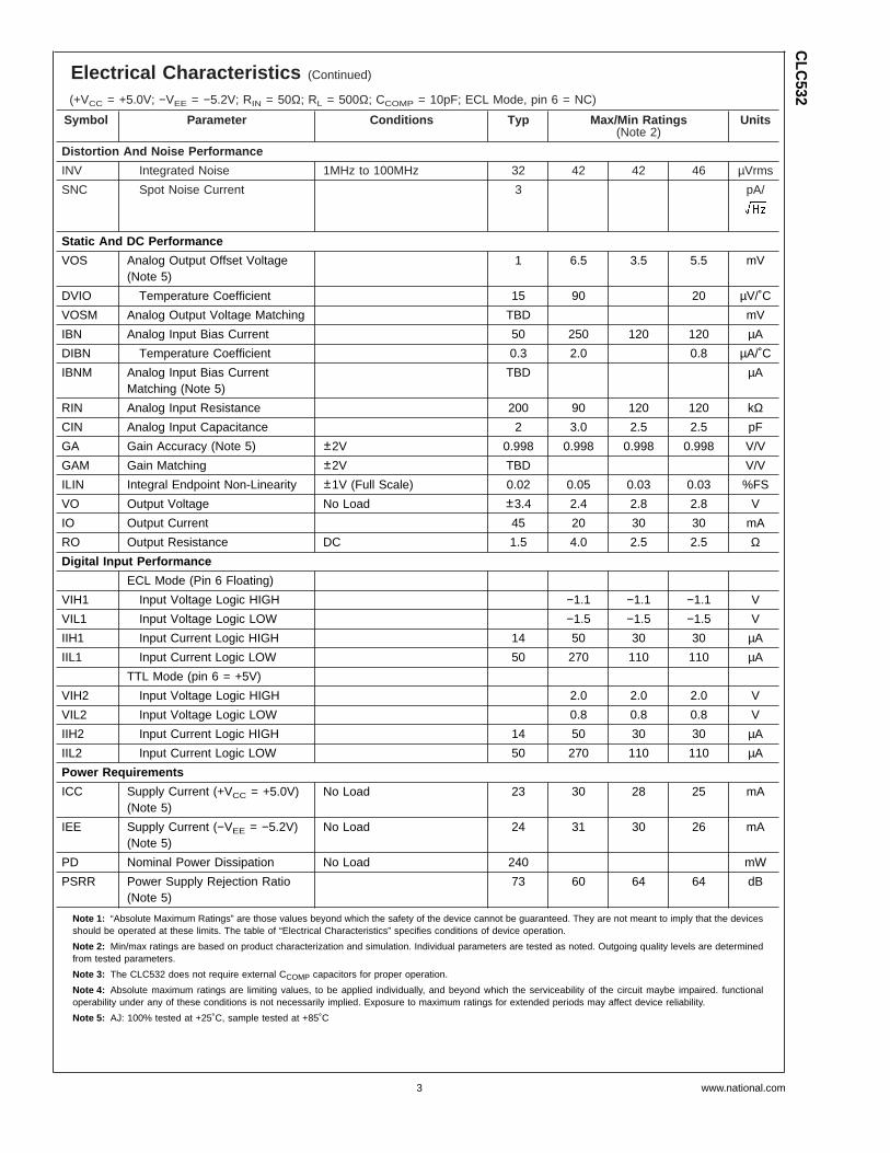
Electrical Characteristics (Continued)
(+VCC = +5.0V; −VEE = −5.2V; RIN = 50Ω; RL = 500Ω; CCOMP = 10pF; ECL Mode, pin 6 = NC)
Symbol Parameter Conditions Typ Max/Min Ratings(Note 2)
Units
Distortion And Noise Performance
INV Integrated Noise 1MHz to 100MHz 32 42 42 46 µVrms
SNC Spot Noise Current 3 pA/
Static And DC Performance
VOS Analog Output Offset Voltage(Note 5)
1 6.5 3.5 5.5 mV
DVIO Temperature Coefficient 15 90 20 µV/˚C
VOSM Analog Output Voltage Matching TBD mV
IBN Analog Input Bias Current 50 250 120 120 µA
DIBN Temperature Coefficient 0.3 2.0 0.8 µA/˚C
IBNM Analog Input Bias CurrentMatching (Note 5)
TBD µA
RIN Analog Input Resistance 200 90 120 120 kΩCIN Analog Input Capacitance 2 3.0 2.5 2.5 pF
GA Gain Accuracy (Note 5) ±2V 0.998 0.998 0.998 0.998 V/V
GAM Gain Matching ±2V TBD V/V
ILIN Integral Endpoint Non-Linearity ±1V (Full Scale) 0.02 0.05 0.03 0.03 %FS
VO Output Voltage No Load ±3.4 2.4 2.8 2.8 V
IO Output Current 45 20 30 30 mA
RO Output Resistance DC 1.5 4.0 2.5 2.5 ΩDigital Input Performance
ECL Mode (Pin 6 Floating)
VIH1 Input Voltage Logic HIGH −1.1 −1.1 −1.1 V
VIL1 Input Voltage Logic LOW −1.5 −1.5 −1.5 V
IIH1 Input Current Logic HIGH 14 50 30 30 µA
IIL1 Input Current Logic LOW 50 270 110 110 µA
TTL Mode (pin 6 = +5V)
VIH2 Input Voltage Logic HIGH 2.0 2.0 2.0 V
VIL2 Input Voltage Logic LOW 0.8 0.8 0.8 V
IIH2 Input Current Logic HIGH 14 50 30 30 µA
IIL2 Input Current Logic LOW 50 270 110 110 µA
Power Requirements
ICC Supply Current (+VCC = +5.0V)(Note 5)
No Load 23 30 28 25 mA
IEE Supply Current (−VEE = −5.2V)(Note 5)
No Load 24 31 30 26 mA
PD Nominal Power Dissipation No Load 240 mW
PSRR Power Supply Rejection Ratio(Note 5)
73 60 64 64 dB
Note 1: “Absolute Maximum Ratings” are those values beyond which the safety of the device cannot be guaranteed. They are not meant to imply that the devicesshould be operated at these limits. The table of “Electrical Characteristics” specifies conditions of device operation.
Note 2: Min/max ratings are based on product characterization and simulation. Individual parameters are tested as noted. Outgoing quality levels are determinedfrom tested parameters.
Note 3: The CLC532 does not require external CCOMP capacitors for proper operation.
Note 4: Absolute maximum ratings are limiting values, to be applied individually, and beyond which the serviceability of the circuit maybe impaired. functionaloperability under any of these conditions is not necessarily implied. Exposure to maximum ratings for extended periods may affect device reliability.
Note 5: AJ: 100% tested at +25˚C, sample tested at +85˚C
CLC
532
www.national.com3
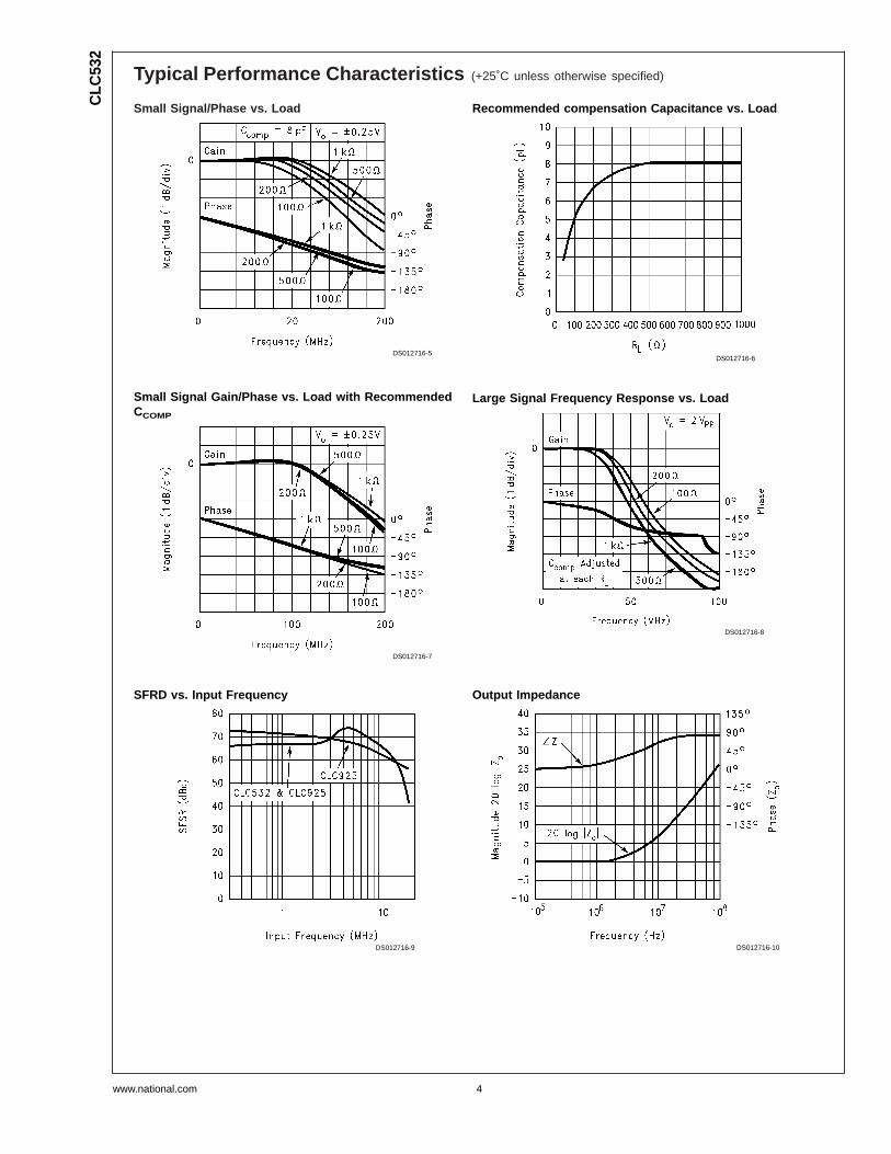
Typical Performance Characteristics (+25˚C unless otherwise specified)
Small Signal/Phase vs. Load
DS012716-5
Recommended compensation Capacitance vs. Load
DS012716-6
Small Signal Gain/Phase vs. Load with RecommendedCCOMP
DS012716-7
Large Signal Frequency Response vs. Load
DS012716-8
SFRD vs. Input Frequency
DS012716-9
Output Impedance
DS012716-10
CLC
532
www.national.com 4

Typical Performance Characteristics (+25˚C unless otherwise specified) (Continued)
Channel to Channel Crosstalk
DS012716-11
Digitized Pulse Response
DS012716-12
Input Impedance
DS012716-13
Small Signal Pulse Response
DS012716-14
Large Signal Pulse Response vs. C comp
DS012716-15
Large Signal Pulse Response vs. R L
DS012716-16
CLC
532
www.national.com5
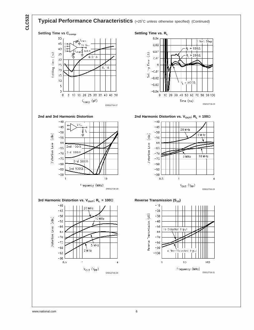
Typical Performance Characteristics (+25˚C unless otherwise specified) (Continued)
Settling Time vs C comp
DS012716-17
Settling Time vs. R L
DS012716-24
2nd and 3rd Harmonic Distortion
DS012716-18
2nd Harmonic Distortion vs. V OUT; RL = 100Ω
DS012716-19
3rd Harmonic Distortion vs. V OUT; RL = 100Ω
DS012716-20
Reverse Transmission (S 12)
DS012716-21
CLC
532
www.national.com 6
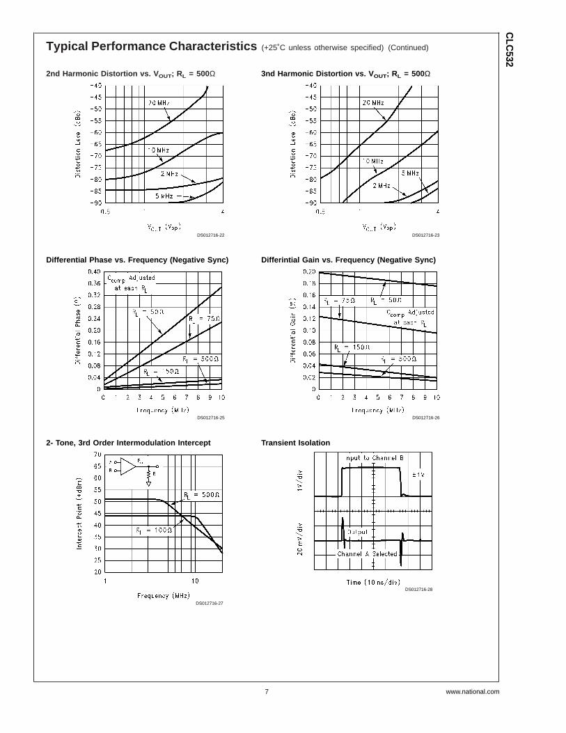
Typical Performance Characteristics (+25˚C unless otherwise specified) (Continued)
2nd Harmonic Distortion vs. V OUT; RL = 500Ω
DS012716-22
3nd Harmonic Distortion vs. V OUT; RL = 500Ω
DS012716-23
Differential Phase vs. Frequency (Negative Sync)
DS012716-25
Differintial Gain vs. Frequency (Negative Sync)
DS012716-26
2- Tone, 3rd Order Intermodulation Intercept
DS012716-27
Transient Isolation
DS012716-28
CLC
532
www.national.com7
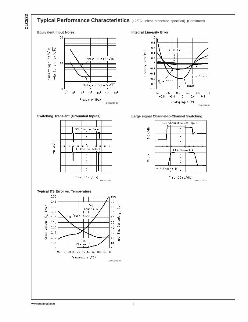
Typical Performance Characteristics (+25˚C unless otherwise specified) (Continued)
Equivalent Input Noise
DS012716-29
Integral Linearity Error
DS012716-30
Switching Transient (Grounded Inputs)
DS012716-31
Large signal Channel-to-Channel Switching
DS012716-32
Typical DS Error vs. Temperature
DS012716-33
CLC
532
www.national.com 8

Application Information
Operation
The CLC532 is a 2:1 analog multiplexer with high impedancebuffered inputs, and a low distortion, output stage. TheCLC532 employs a closed-loop design, which dramaticallyimproves distortion performance. The channel SELECT con-trol Figure 1 determines which of the two inputs (INA or INB)is present at the OUTPUT. Beyond the basic multiplexerfunction, the CLC532 offers compatibility with either TTL orECL logic families, as well as adjustable bandwidth.
Digital Interface and Channel SELECT
The CLC532 functions with ECL, TTL and CMOS logic fami-lies, DREF controls logic compatibility. In normal operation,DREF is left floating, and the channel SELECT responds toECL level signals, Figure 2. For TTL or CMOS level SELECTinputs (Figure 3), DREF should be tied to +5V (the CLC532incorporates an internal 2300Ω series isolation resistor forthe DREF input). For TTL or CMOS operation, the channelSELECT requires a resistor input network to prevent satura-tion of the channel select circuitry. Without this input net-work, channel SELECT logic levels above 3V will causeinternal junction saturation and slow switching speeds.
Compensation
The CLC532 incorporates compensation nodes that allowboth its bandwidth and its settling time/slew rate to be ad-justed. Bandwidth and settling time/slew adjustments arelinked, meaning that lowering the bandwidth also lowersslew rate and lengthens settling time. Proper compensationis necessary to optimize system performance. Time domainapplications should generally be optimized for lowest RMSnoise at the CLC532 output, while maintaining settling timeand slew rate at adequate levels to meet system needs.Frequency Domain applications should generally be opti-mized for maximally flat frequency response.
System Timing Diagram
ASELECT
B
SWT90SWT10
90%
10%
TSx
TRx TRx
SETTLING ERRORWINDOW
CHANNEL A = +1VCHANNEL B = - 1V
OS
... where TSx is TS14 or TSP or TSS,and TRx is TRS ro TSL.
OUTPUT
DS012716-34
System Transient Timing Diagram
ASELECT
B
ST 2ns~~
OUTPUT
Channel A = 0VChannel B = 0V
DS012716-35
RL
RIN
RIN
5
INB 8
106
9
INA
43
21
7
1314
VOUT
12
CHANNEL A
CHANNEL B
CHANNELSELECT
DGND
-5.2V
0.1µF
CCOMP2
CCOMP1
+5V
CLC532
DREF
11
0.1 µF
+6.8 µF
+6.8 µF
DS012716-36
FIGURE 1. Standard CLC532 Circuit Configuration
DS012716-37
FIGURE 2. ECL Level Channel SELECT Configuration
DS012716-38
FIGURE 3. TTL/CMOS Level Channel SELECTConfiguration
CLC
532
www.national.com9

Application Information (Continued)
Figure 4 below describes the basic relationship betweensettling time (TS) and RS for various values of load capaci-tance, CL, where CCOMP = 10pF
Figure 5 shows the resulting changes in bandwidth and slewrate for increasing values of CCOMP. The RMS noise at theCLC532 output can be approximated as:
where.... nV = input spot noise voltage;
BW−3dB = Bandwidth is from Figure 5.
Power Supplies and Grounding
Proper power supply bypassing and grounding is essentialto the CLC532’s operation. 0.1µF to .1µF ceramic chip ca-pacitor should be located very close to the individual powersupply pins. Larger +6.8µF tantalum capacitors should beused within a few inches of the CLC532. The ground con-nections for these larger by-pass capacitors should be sym-metrically located relative the CLC532 output load groundconnection. Harmonic distortion can be heavily influenced bynon-symmetric decoupling capacitor grounding. The smallerchip capacitors located directly at the power supply pins arenot particularly susceptible to this effect.
Separation of analog and digital ground planes is not recom-mended. In most cases, a single low impedance ground
plane will provide the best performance. In those specialcases requiring separate ground planes, the following tableindicates the signal and supply ground connections.
Pin Functions Ground Return
1,3 Shield/Supply Returns Supplies andInputs
5 DREF Ground DREF Currentsonly
Input Shielding
The CLC532 has been designated for use in high speedwide dynamic range systems. Guarding traces and the useof the ground pins separating the analog inputs are recom-mended to maintain high isolation (Figure 6). Likely sourcesof noise and interference that may couple onto the inputs,are the logic signals and power supplies to the CLC532.Other types if clock and signal traces should not be over-looked, however.
The general rule in maintaining isolation has two facets,minimize the primary return ground current path impedancesback to the respective signal sources, while maximizing theimpedance associated with common or secondary groundcurrent return paths. Success or failure to optimize inputsignal isolation can be measured directly as the isolationbetween the input channels with the CLC532 removed fromcircuit. The channel-to -channel isolation of the CLC532 cannever be better than the isolation level present at its inputs.
Special attention must be paid to input termination resistors.Minimizing the return current path that is common to both ofthe input termination resistors is essential. In the event that aground return current from one input termination resistor isable to find a secondary path back to its signal source (whichalso happens to be common with either the primary or sec-ondary return path for the second input termination resistor),a small voltage can appear across the second input termi-nation resistor. The small voltage seen across the secondinput termination resistor will be highly correlated with thesignal generating the initial return currents. This situation willseverely degrade channel-to-channel isolation at the input ofthe CLC532, even if the CLC532 were removed from circuit.Poor isolation at the input will be transmitted directly to theoutput.
Use of “small” value input termination resistors will alsoimprove channel-to-channel isolation. However, extremelylow values (<25Ω) tend to stress the driving source’s abilityto provide a high-quality input signal to the CLC532. Highervalues tend to aggravate any layout dependent crosstalk.75Ω to 50Ω is a reasonable target, but the lower the better.
DS012716-39
FIGURE 4. Settling Time and R S vs. CL
DS012716-41
FIGURE 5. CCOMP for Maximally Flat FrequencyResponse
Channel AConnector
Channel BConnector
Chip Resistors
Pin 1
DS012716-42
FIGURE 6. Alternate Layout Using Guard Ring
CLC
532
www.national.com 10
Application Information (Continued)
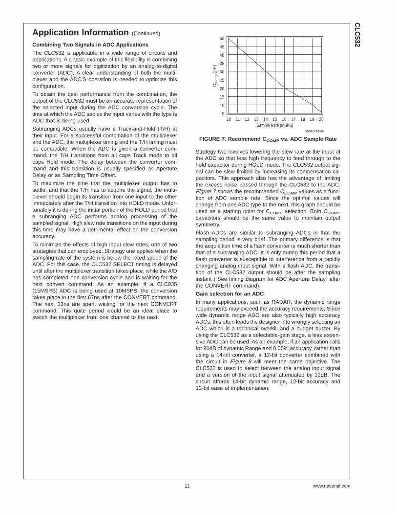
Combining Two Signals in ADC Applications
The CLC532 is applicable in a wide range of circuits andapplications. A classic example of this flexibility is combiningtwo or more signals for digitization by an analog-to-digitalconverter (ADC). A clear understanding of both the multi-plexer and the ADC’S operation is needed to optimize thisconfiguration.
To obtain the best performance from the combination, theoutput of the CLC532 must be an accurate representation ofthe selected input during the ADC conversion cycle. Thetime at which the ADC saples the input varies with the type isADC that is being used.
Subranging ADCs usually have a Track-and-Hold (T/H) attheir input. For a successful combination of the multiplexerand the ADC, the multiplexer timing and the T/H timing mustbe compatible. When the ADC is given a converter com-mand, the T/H transitions from all caps Track mode to allcaps Hold mode. The delay between the converter com-mand and this transition is usually specified as ApertureDelay or as Sampling Time Offset.
To maximize the time that the multiplexer output has tosettle, and that the T/H has to acquire the signal, the multi-plexer should begin its transition from one input to the otherimmediately after the T/H transition into HOLD mode. Unfor-tunately it is during the initial portion of the HOLD period thata subranging ADC performs analog processing of thesampled signal. High slew rate transitions on the input duringthis time may have a detrimental effect on the conversionaccuracy.
To minimize the effects of high input slew rates, one of twostrategies that can employed. Strategy one applies when thesampling rate of the system is below the rated speed of theADC. For this case, the CLC532 SELECT timing is delayeduntil after the multiplexer transition takes place, while the A/Dhas completed one conversion cycle and is waiting for thenext convert command. As an example, if a CLC935(15MSPS) ADC is being used at 10MSPS, the conversiontakes place in the first 67ns after the CONVERT command.The next 33ns are spent waiting for the next CONVERTcommand. This quite period would be an ideal place toswitch the multiplexer from one channel to the next.
Strategy two involves lowering the slew rate at the input ofthe ADC so that less high frequency to feed through to thehold capacitor during HOLD mode. The CLC532 output sig-nal can be slew limited by increasing its compensation ca-pacitors. This approach also has the advantage of limitingthe excess noise passed through the CLC532 to the ADC.Figure 7 shows the recommended CCOMP values as a func-tion of ADC sample rate. Since the optimal values willchange from one ADC type to the next, this graph should beused as a starting point for CCOMP selection. Both CCOMP
capacitors should be the same value to maintain outputsymmetry.
Flash ADCs are similar to subranging ADCs in that thesampling period is very brief. The primary difference is thatthe acquisition time of a flash converter is much shorter thanthat of a subranging ADC. It is only during this period that aflash converter is susceptible to interference from a rapidlychanging analog input signal. With a flash ADC, the transi-tion of the CLC532 output should be after the samplinginstant (”See timing diagram for ADC Aperture Delay” afterthe CONVERT command).
Gain selection for an ADC
In many applications, such as RADAR, the dynamic rangerequirements may exceed the accuracy requirements. Sincewide dynamic range ADC are also typically high accuracyADCs, this often leads the designer into wrongly selecting anADC which is a technical overkill and a budget buster. Byusing the CLC532 as a selectable-gain stage, a less expen-sive ADC can be used. As an example, if an application callsfor 80dB of dynamic Range and 0.05% accuracy, rather thanusing a 14-bit converter, a 12-bit converter combined withthe circuit in Figure 8 will meet the same objective. TheCLC532 is used to select between the analog input signaland a version of the input signal attenuated by 12dB. Thecircuit affords 14-bit dynamic range, 12-bit accuracy and12-bit ease of implementation.
Sample Rate (MSPS)
Cco
mp
(pF
)
10 11 12 13 14 15 16 17 18 19 20
50
45
40
35
30
25
20
15
10
5
DS012716-43
FIGURE 7. Recommend C COMP vs. ADC Sample Rate
CLC
532
www.national.com11
Application Information (Continued)
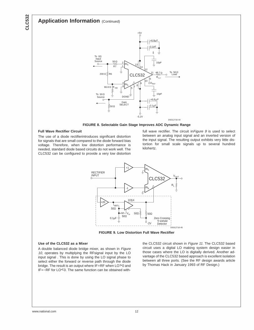
Full Wave Rectifier Circuit
The use of a diode rectifierintroduces significant distortionfor signals that are small compared to the diode forward biasvoltage. Therefore, when low distortion performance isneeded, standard diode based circuits do not work well. TheCLC532 can be configured to provide a very low distortion
full wave rectifier. The circuit inFigure 9 is used to selectbetween an analog input signal and an inverted version ofthe input signal. The resulting output exhibits very little dis-tortion for small scale signals up to several hundredkilohertz.
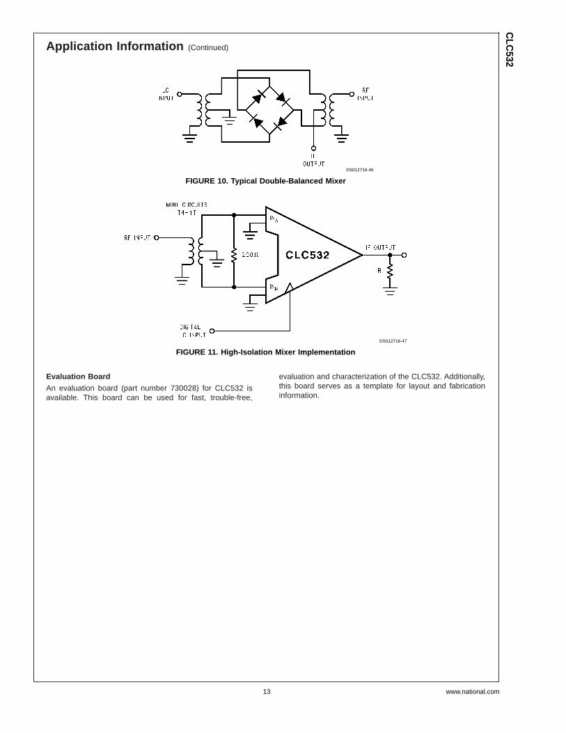
Use of the CLC532 as a Mixer
A double balanced diode bridge mixer, as shown in Figure10, operates by multiplying the RFsignal input by the LOinput signal . This is done by using the LO signal phase toselect either the forward or reverse path through the diodebridge. The result is an output where IF=RF when LO>0 andIF=−RF for LO<0. The same function can be obtained with-
the CLC532 circuit shown in Figure 11. The CLC532 basedcircuit uses a digital LO making system design easier inthose cases where the LO is digitally derived. Another ad-vantage of the CLC532 based approach is excellent isolationbetween all three ports. (See the RF design awards articleby Thomas Hack in January 1993 of RF Design.)
CLC532
µ
FGain
SELECT
0.1 F
F
µ
R
48.7
5
INB 8
106
9
INA
43
21
7
1314
12
DGND
-5.2V
0.1µF
+5V
DREF
11
µ
+6.8
+6.8
10pF
10pF
50 Ω
50 Ω
OUT
Ω 50 ΩToLoad
50 ΩToSource
Ω200
Ω66.6
0ΩTo
SourceInput
R7
R6
R INB
DS012716-44
FIGURE 8. Selectable Gain Stage Improves ADC Dynamic Range
10114
50Ω
50Ω
50Ω50Ω
-2V
RLINB
INA
VOUTCLC532
VBB
0.1µF
+1
-1
+20
RECTIFIERINPUT
Zero Crossing Tr esholdDetector
DS012716-45
FIGURE 9. Low Distortion Full Wave Rectifier
CLC
532
www.national.com 12
Application Information (Continued)
Evaluation Board
An evaluation board (part number 730028) for CLC532 isavailable. This board can be used for fast, trouble-free,
evaluation and characterization of the CLC532. Additionally,this board serves as a template for layout and fabricationinformation.
DS012716-46
FIGURE 10. Typical Double-Balanced Mixer
DS012716-47
FIGURE 11. High-Isolation Mixer Implementation
CLC
532
www.national.com13
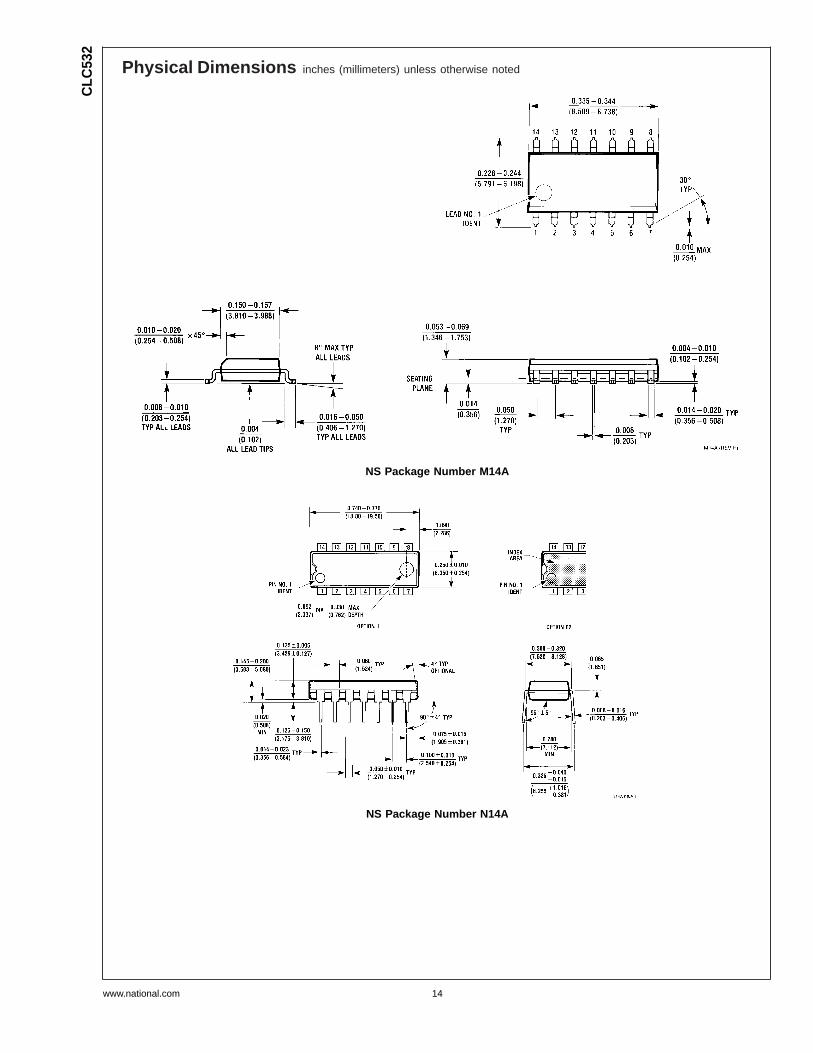
Physical Dimensions inches (millimeters) unless otherwise noted
NS Package Number M14A
NS Package Number N14A
CLC
532
www.national.com 14

Notes
LIFE SUPPORT POLICY
NATIONAL’S PRODUCTS ARE NOT AUTHORIZED FOR USE AS CRITICAL COMPONENTS IN LIFE SUPPORTDEVICES OR SYSTEMS WITHOUT THE EXPRESS WRITTEN APPROVAL OF THE PRESIDENT AND GENERALCOUNSEL OF NATIONAL SEMICONDUCTOR CORPORATION. As used herein:
1. Life support devices or systems are devices orsystems which, (a) are intended for surgical implantinto the body, or (b) support or sustain life, andwhose failure to perform when properly used inaccordance with instructions for use provided in thelabeling, can be reasonably expected to result in asignificant injury to the user.
2. A critical component is any component of a lifesupport device or system whose failure to performcan be reasonably expected to cause the failure ofthe life support device or system, or to affect itssafety or effectiveness.
National SemiconductorCorporationAmericasEmail: [email protected]
National SemiconductorEurope
Fax: +49 (0) 180-530 85 86Email: [email protected]
Deutsch Tel: +49 (0) 69 9508 6208English Tel: +44 (0) 870 24 0 2171Français Tel: +33 (0) 1 41 91 8790
National SemiconductorAsia Pacific CustomerResponse GroupTel: 65-2544466Fax: 65-2504466Email: [email protected]
National SemiconductorJapan Ltd.Tel: 81-3-5639-7560Fax: 81-3-5639-7507
www.national.com
CLC
532H
ighS
peed2:1
Analog
Multiplexer
National does not assume any responsibility for use of any circuitry described, no circuit patent licenses are implied and National reserves the right at any time without notice to change said circuitry and specifications.