Embed Size (px)
Citation preview
OPA875
1FEATURES DESCRIPTION
APPLICATIONS
OPA875
(Patented)
75W
Ch 0
75W
Ch 1
Out
EN
75W
SEL
Channel Select
2:1 Video Multiplexer
OPA875
www.ti.com ............................................................................................................................................ SBOS340C–DECEMBER 2006–REVISED AUGUST 2008
Single 2:1 High-Speed Video Multiplexer
2• 700MHz SMALL-SIGNAL BANDWIDTH The OPA875 offers a very wideband, single-channel(AV = +2) 2:1 multiplexer in an SO-8 or a small MSOP-8
package. Using only 11mA, the OPA875 provides a• 425MHz, 4VPP BANDWIDTHgain of +2 video amplifier channel with greater• 0.1dB GAIN FLATNESS to 200MHz than 425MHz large-signal bandwidth (4VPP). Gain
• 4ns CHANNEL SWITCHING TIME accuracy and switching glitch are improved overearlier solutions using a new input stage switching• LOW SWITCHING GLITCH: 40mVPPapproach. This technique uses current steering as the• 3100V/µs SLEW RATE input switch while maintaining an overall closed-loop
• 0.025%/0.025° DIFFERENTIAL GAIN, PHASE design. With greater than 700MHz small-signalbandwidth at a gain of 2, the OPA875 gives a typical• HIGH GAIN ACCURACY: 2.0V/V ±0.4%0.1dB gain flatness to greater than 200MHz.
System power may be reduced using the chip enable• RGB SWITCHING feature for the OPA875. Taking the chip enable line
high powers down the OPA875 to less than 300µA• LCD PROJECTOR INPUT SELECTtotal supply current. Muxing multiple OPA875 outputs• WORKSTATION GRAPHICStogether, then using the chip enable to select which• ADC INPUT MUX channels are active, increases the number of possible
• DROP-IN UPGRADE TO LT1675-1 inputs.
Where three channels are required, consider usingthe OPA3875 for the same level of performance.
OPA875 RELATED PRODUCTSDESCRIPTION
OPA3875 Triple-Channel OPA875OPA692 225MHz Video BufferOPA693 700MHz Video Buffer
1
Please be aware that an important notice concerning availability, standard warranty, and use in critical applications of TexasInstruments semiconductor products and disclaimers thereto appears at the end of this data sheet.
2All trademarks are the property of their respective owners.
PRODUCTION DATA information is current as of publication date. Copyright © 2006–2008, Texas Instruments IncorporatedProducts conform to specifications per the terms of the TexasInstruments standard warranty. Production processing does notnecessarily include testing of all parameters.
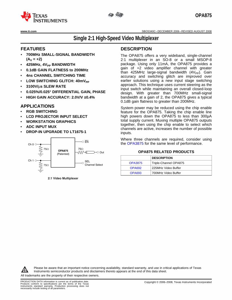
ABSOLUTE MAXIMUM RATINGS (1)
1
2
3
4
8
7
6
5
GND
Channel 1 (V1)
-VS
Output (V )OUT
Channel Select (SEL)
+VS
Chip Enable ( )EN
Channel 0 (V0)
OPA875
MSOP, SOTop View
402 W402 W
OPA875
SBOS340C–DECEMBER 2006–REVISED AUGUST 2008 ............................................................................................................................................ www.ti.com
This integrated circuit can be damaged by ESD. Texas Instruments recommends that all integrated circuits be handled withappropriate precautions. Failure to observe proper handling and installation procedures can cause damage.
ESD damage can range from subtle performance degradation to complete device failure. Precision integrated circuits may be moresusceptible to damage because very small parametric changes could cause the device not to meet its published specifications.
ORDERING INFORMATIONSPECIFIED
PACKAGE- PACKAGE TEMPERATURE PACKAGE ORDERING TRANSPORTPRODUCT LEAD DESIGNATOR RANGE MARKING NUMBER MEDIA, QUANTITY
OPA875ID Rails, 75OPA875 SO-8 D –40°C to +85°C OPA875
OPA875IDR Tape and Reel, 2500OPA875IDGKT Tape and Reel, 250
OPA875 MSOP-8 DGK –40°C to +85°C BPLOPA875IDGKR Tape and Reel, 2500
Over operating temperature range, unless otherwise noted.
OPA875 UNITPower Supply ±6.5 VInternal Power Dissipation See Thermal AnalysisInput Voltage Range ±VS VStorage Temperature Range –65 to +125 °CLead Temperature (soldering, 10s) +260 °COperating Junction Temperature +150 °CContinuous Operating Junction Temperature +140 °CESD Rating:
Human Body Model (HBM) 2000 VCharged Device Model (CDM) 1500 VMachine Model (MM) 200 V
(1) Stresses above these ratings may cause permanent damage. Exposure to absolute maximum conditions for extended periods maydegrade device reliability. These are stress ratings only, and functional operation of the device at these or any other conditions beyondthose specified is not implied.
PIN CONFIGURATIONTable 1. TRUTH TABLEOPA875
SELECT ENABLE VOUT
1 0 R00 0 R1X 1 Off
2 Submit Documentation Feedback Copyright © 2006–2008, Texas Instruments Incorporated
Product Folder Link(s): OPA875
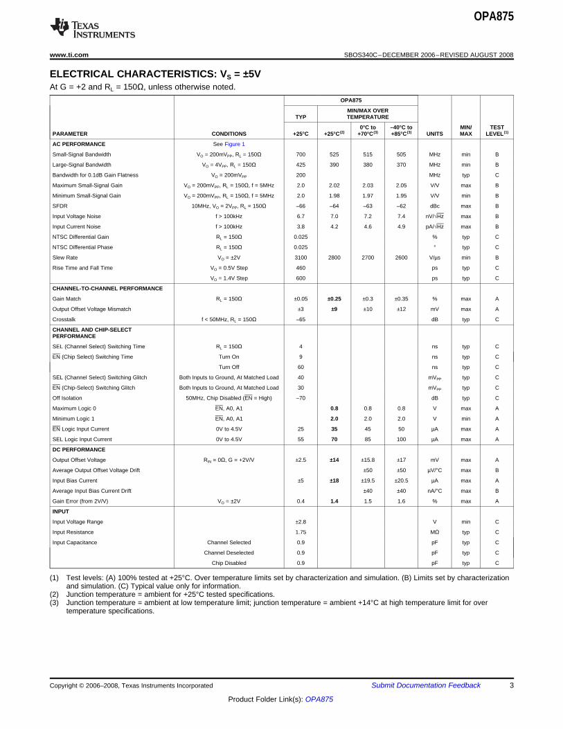
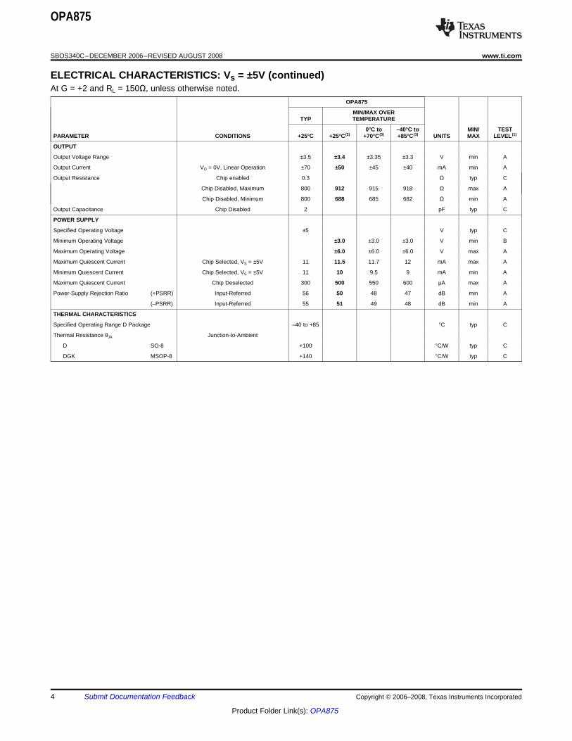
ELECTRICAL CHARACTERISTICS: VS = ±5V
OPA875
www.ti.com ............................................................................................................................................ SBOS340C–DECEMBER 2006–REVISED AUGUST 2008
At G = +2 and RL = 150Ω, unless otherwise noted.OPA875
MIN/MAX OVERTYP TEMPERATURE
0°C to –40°C to MIN/ TESTPARAMETER CONDITIONS +25°C +25°C (2) +70°C (3) +85°C(3) UNITS MAX LEVEL (1)
AC PERFORMANCE See Figure 1
Small-Signal Bandwidth VO = 200mVPP, RL = 150Ω 700 525 515 505 MHz min B
Large-Signal Bandwidth VO = 4VPP, RL = 150Ω 425 390 380 370 MHz min B
Bandwidth for 0.1dB Gain Flatness VO = 200mVPP 200 MHz typ C
Maximum Small-Signal Gain VO = 200mVPP, RL = 150Ω, f = 5MHz 2.0 2.02 2.03 2.05 V/V max B
Minimum Small-Signal Gain VO = 200mVPP, RL = 150Ω, f = 5MHz 2.0 1.98 1.97 1.95 V/V min B
SFDR 10MHz, VO = 2VPP, RL = 150Ω –66 –64 –63 –62 dBc max B
Input Voltage Noise f > 100kHz 6.7 7.0 7.2 7.4 nV/√Hz max B
Input Current Noise f > 100kHz 3.8 4.2 4.6 4.9 pA/√Hz max B
NTSC Differential Gain RL = 150Ω 0.025 % typ C
NTSC Differential Phase RL = 150Ω 0.025 ° typ C
Slew Rate VO = ±2V 3100 2800 2700 2600 V/µs min B
Rise Time and Fall Time VO = 0.5V Step 460 ps typ C
VO = 1.4V Step 600 ps typ C
CHANNEL-TO-CHANNEL PERFORMANCE
Gain Match RL = 150Ω ±0.05 ±0.25 ±0.3 ±0.35 % max A
Output Offset Voltage Mismatch ±3 ±9 ±10 ±12 mV max A
Crosstalk f < 50MHz, RL = 150Ω –65 dB typ C
CHANNEL AND CHIP-SELECTPERFORMANCE
SEL (Channel Select) Switching Time RL = 150Ω 4 ns typ C
EN (Chip Select) Switching Time Turn On 9 ns typ C
Turn Off 60 ns typ C
SEL (Channel Select) Switching Glitch Both Inputs to Ground, At Matched Load 40 mVPP typ C
EN (Chip-Select) Switching Glitch Both Inputs to Ground, At Matched Load 30 mVPP typ C
Off Isolation 50MHz, Chip Disabled (EN = High) –70 dB typ C
Maximum Logic 0 EN, A0, A1 0.8 0.8 0.8 V max A
Minimum Logic 1 EN, A0, A1 2.0 2.0 2.0 V min A
EN Logic Input Current 0V to 4.5V 25 35 45 50 µA max A
SEL Logic Input Current 0V to 4.5V 55 70 85 100 µA max A
DC PERFORMANCE
Output Offset Voltage RIN = 0Ω, G = +2V/V ±2.5 ±14 ±15.8 ±17 mV max A
Average Output Offset Voltage Drift ±50 ±50 µV/°C max B
Input Bias Current ±5 ±18 ±19.5 ±20.5 µA max A
Average Input Bias Current Drift ±40 ±40 nA/°C max B
Gain Error (from 2V/V) VO = ±2V 0.4 1.4 1.5 1.6 % max A
INPUT
Input Voltage Range ±2.8 V min C
Input Resistance 1.75 MΩ typ C
Input Capacitance Channel Selected 0.9 pF typ C
Channel Deselected 0.9 pF typ C
Chip Disabled 0.9 pF typ C
(1) Test levels: (A) 100% tested at +25°C. Over temperature limits set by characterization and simulation. (B) Limits set by characterizationand simulation. (C) Typical value only for information.
(2) Junction temperature = ambient for +25°C tested specifications.(3) Junction temperature = ambient at low temperature limit; junction temperature = ambient +14°C at high temperature limit for over
temperature specifications.
Copyright © 2006–2008, Texas Instruments Incorporated Submit Documentation Feedback 3
Product Folder Link(s): OPA875
OPA875
SBOS340C–DECEMBER 2006–REVISED AUGUST 2008 ............................................................................................................................................ www.ti.com
ELECTRICAL CHARACTERISTICS: VS = ±5V (continued)At G = +2 and RL = 150Ω, unless otherwise noted.
OPA875
MIN/MAX OVERTYP TEMPERATURE
0°C to –40°C to MIN/ TESTPARAMETER CONDITIONS +25°C +25°C (2) +70°C (3) +85°C(3) UNITS MAX LEVEL (1)
OUTPUT
Output Voltage Range ±3.5 ±3.4 ±3.35 ±3.3 V min A
Output Current VO = 0V, Linear Operation ±70 ±50 ±45 ±40 mA min A
Output Resistance Chip enabled 0.3 Ω typ C
Chip Disabled, Maximum 800 912 915 918 Ω max A
Chip Disabled, Minimum 800 688 685 682 Ω min A
Output Capacitance Chip Disabled 2 pF typ C
POWER SUPPLY
Specified Operating Voltage ±5 V typ C
Minimum Operating Voltage ±3.0 ±3.0 ±3.0 V min B
Maximum Operating Voltage ±6.0 ±6.0 ±6.0 V max A
Maximum Quiescent Current Chip Selected, VS = ±5V 11 11.5 11.7 12 mA max A
Minimum Quiescent Current Chip Selected, VS = ±5V 11 10 9.5 9 mA min A
Maximum Quiescent Current Chip Deselected 300 500 550 600 µA max A
Power-Supply Rejection Ratio (+PSRR) Input-Referred 56 50 48 47 dB min A
(–PSRR) Input-Referred 55 51 49 48 dB min A
THERMAL CHARACTERISTICS
Specified Operating Range D Package –40 to +85 °C typ C
Thermal Resistance θJA Junction-to-Ambient
D SO-8 +100 °C/W typ C
DGK MSOP-8 +140 °C/W typ C
4 Submit Documentation Feedback Copyright © 2006–2008, Texas Instruments Incorporated
Product Folder Link(s): OPA875
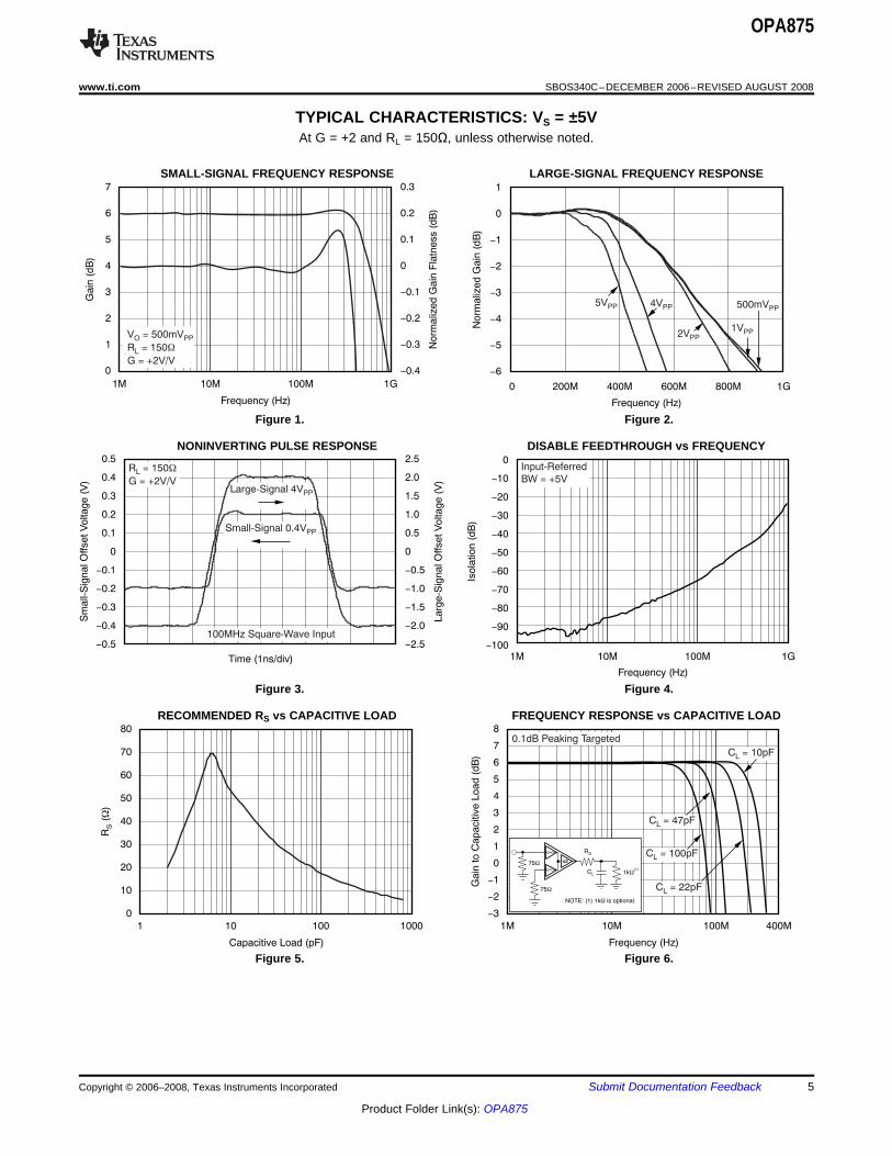
TYPICAL CHARACTERISTICS: VS = ±5V
7
6
5
4
3
2
1
0
Gain
(dB
)
0.3
0.2
0.1
0
-0.1
-0.2
-0.3
-0.4
Norm
aliz
ed G
ain
Fla
tness (
dB
)
Frequency (Hz)
1M 10M 100M 1G
VO PP= 500mV
R WL = 150
G = +2V/V
Norm
aliz
ed G
ain
(dB
)
Frequency (Hz)
1
0
-1
-2
-3
-4
-5
-6
0 200M 1G
5VPP
2VPP1VPP
4VPP
400M 600M 800M
500mVPP
0.5
0.4
0.3
0.2
0.1
0
-0.1
-0.2
-0.3
-0.4
-0.5
2.5
2.0
1.5
1.0
0.5
0
-0.5
-1.0
-1.5
-2.0
-2.5
Sm
all-
Sig
nal O
ffset V
oltage (
V)
Larg
e-S
ignal O
ffset V
oltage (
V)
Time (1ns/div)
Large-Signal 4VPP
Small-Signal 0.4VPP
R = 150WL
G = +2V/V
100MHz Square-Wave Input
0
-10
-20
-30
-40
-50
-60
-70
-80
-90
-100
Frequency (Hz)
Isola
tion (
dB
)
1M 10M 100M 1G
Input-Referred
BW = +5V
80
70
60
50
40
30
20
10
0
R)
W(S
Capacitive Load (pF)
1 10 100 1000
8
7
6
5
4
3
2
1
0
-1
-2
-3
Gain
to C
apacitiv
e L
oad (
dB
)
Frequency (Hz)
1M 10M 100M 400M
0.1dB Peaking Targeted
C = 47pFL
C = 100pFL
C = 10pFL
C = 22pFL
RS
75W
1kW(1)
CL
75W
NOTE: (1) 1k is optional.W
x2
OPA875
www.ti.com ............................................................................................................................................ SBOS340C–DECEMBER 2006–REVISED AUGUST 2008
At G = +2 and RL = 150Ω, unless otherwise noted.
SMALL-SIGNAL FREQUENCY RESPONSE LARGE-SIGNAL FREQUENCY RESPONSE
Figure 1. Figure 2.
NONINVERTING PULSE RESPONSE DISABLE FEEDTHROUGH vs FREQUENCY
Figure 3. Figure 4.
RECOMMENDED RS vs CAPACITIVE LOAD FREQUENCY RESPONSE vs CAPACITIVE LOAD
Figure 5. Figure 6.
Copyright © 2006–2008, Texas Instruments Incorporated Submit Documentation Feedback 5
Product Folder Link(s): OPA875
-60
-65
-70
-75
-80
-85
-90
Harm
onic
Dis
tort
ion (
dB
c)
Resistance ( )W
100 1k
V = 2VO PP
f = 10MHz
2nd-Harmonic
3rd-Harmonic
dBc = dB Below Carrier
-40
-45
-50
-55
-60
-65
-70
-75
-80
-85
-90
-95
Harm
onic
Dis
tort
ion (
dB
c)
Supply Voltage ( V )± S
±2.5 ±3.0 ±3.5 ±4.0 ±4.5 ±5.0 ±5.5 ±6.0
V = 2VO PP
R = 150WL
f = 10MHz
3rd-Harmonic
2nd-Harmonic
dBc = dB Below Carrier
-40
-45
-50
-55
-60
-65
-70
-75
-80
-85
-90
-95
Harm
onic
Dis
tort
ion (
dB
c)
Frequency (Hz)
1M 10M 100M
V = 2VO PP
R = 150L W
2nd-Harmonic
3rd-Harmonic
dBc = dB Below Carrier
-55
-60
-65
-70
-75
-80
-85
-90
-95
-100
-105
Harm
onic
Dis
tort
ion (
dB
c)
Output Voltage Swing (V )PP
0.5 1.5 2.5 3.5 4.5 5.5 6.5 7.0
R = 150L W
f = 10MHz
dBc = dB Below Carrier
2nd-Harmonic
3rd-Harmonic
-50
-60
-70
-80
-90
-100
Third-O
rder
Spurious L
evel (d
Bc)
Single-Tone Load Power (dBm)
-6 -4 -2 0 2 4 6 8 10
R = 100WL
Load Power at Matched 50 LoadW
dBc = dB Below Carrier
50MHz
20MHz 10MHz
5
4
3
2
1
0
-1
-2
-3
-4
-5
V(V
)O
UT
I (mA)O
-200 -150 -100 -50 0 50 100 150 200
1W Internal
1W Internal
Power Limit
50 Load LineW
100 Load LineW
25 Load LineW
Power Limit
OPA875
SBOS340C–DECEMBER 2006–REVISED AUGUST 2008 ............................................................................................................................................ www.ti.com
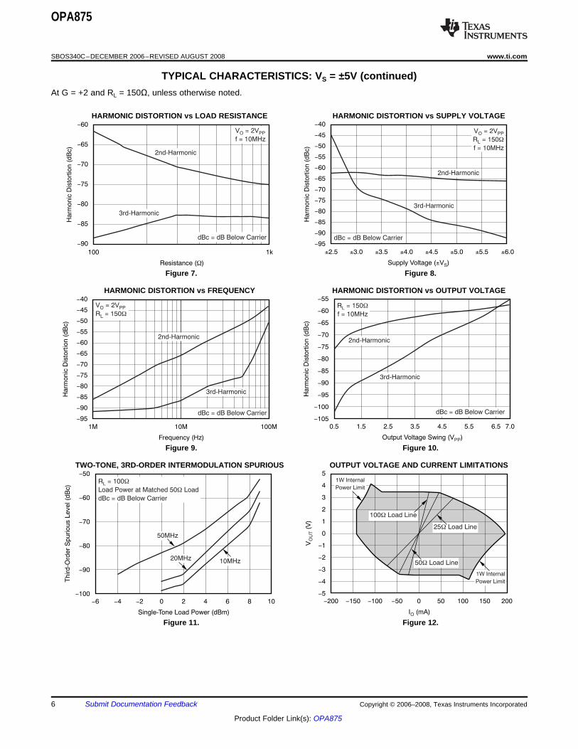
TYPICAL CHARACTERISTICS: VS = ±5V (continued)At G = +2 and RL = 150Ω, unless otherwise noted.
HARMONIC DISTORTION vs LOAD RESISTANCE HARMONIC DISTORTION vs SUPPLY VOLTAGE
Figure 7. Figure 8.
HARMONIC DISTORTION vs FREQUENCY HARMONIC DISTORTION vs OUTPUT VOLTAGE
Figure 9. Figure 10.
TWO-TONE, 3RD-ORDER INTERMODULATION SPURIOUS OUTPUT VOLTAGE AND CURRENT LIMITATIONS
Figure 11. Figure 12.
6 Submit Documentation Feedback Copyright © 2006–2008, Texas Instruments Incorporated
Product Folder Link(s): OPA875
1.5
1.0
0.5
0
-0.5
-1.0
-1.5
3.5
3.0
2.5
2.0
1.5
1.0
0.5
0
-0.5
Outp
ut V
oltage (
V)
Channel S
ele
ct (V
)
Time (5ns/div)
Output Voltage
VSEL
RL = 150W
V R = 400MHz, 1VIN_ I PP
V R = 0VIN_ O DC
1.5
1.0
0.5
0
-0.5
-1.0
-1.5
3.5
3.0
2.5
2.0
1.5
1.0
0.5
0
-0.5
Outp
ut V
oltage (
V)
Channel S
ele
ct (V
)
Time (5ns/div)
Output Voltage
VSEL
VIN_ DCCh0 = +0.5V
V Ch1 = 0.5V-IN_ DC
Outp
ut (m
V)
Channel S
ele
ct (V
)
Time (10ns/div)
At Matched Load
VSEL
7.5
5.0
2.5
0
-2.5
30
20
10
0
-10
-20
1.5
1.0
0.5
0
-0.5
-1.0
-1.5
3.5
3.0
2.5
2.0
1.5
1.0
0.5
0
-0.5
Outp
ut
Vo
lta
ge
(V
)
En
ab
le V
oltag
e (
V)
Time (20ns/div)
Output Voltage
VEN
V Ch1 = 0VIN_
VIN_Ch0 = 200MHz, 1VPP
Ou
tpu
t (m
V)
Time (100ns/div)
En
ab
le V
olta
ge
(V
)
5.0
2.5
0
-2.5
VEN
At Matched Load15
10
5
0
-5
-10
-15 Outp
ut (V
)
Frequency (Hz)
0
-10
-20
-30
-40
-50
-60
-70
-80
-90
-100
-110
1M 10M 100M 1G
Ch 0 Selected
Ch 1 Driven
Input-Referred
Ch 1 Selected
Ch 0 Driven
OPA875
www.ti.com ............................................................................................................................................ SBOS340C–DECEMBER 2006–REVISED AUGUST 2008
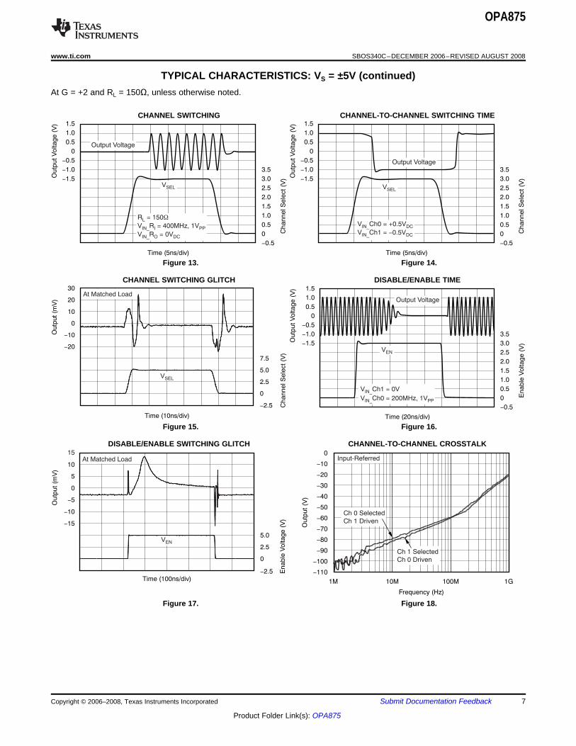
TYPICAL CHARACTERISTICS: VS = ±5V (continued)At G = +2 and RL = 150Ω, unless otherwise noted.
CHANNEL SWITCHING CHANNEL-TO-CHANNEL SWITCHING TIME
Figure 13. Figure 14.
CHANNEL SWITCHING GLITCH DISABLE/ENABLE TIME
Figure 15. Figure 16.
DISABLE/ENABLE SWITCHING GLITCH CHANNEL-TO-CHANNEL CROSSTALK
Figure 17. Figure 18.
Copyright © 2006–2008, Texas Instruments Incorporated Submit Documentation Feedback 7
Product Folder Link(s): OPA875
10k
1k
100
10
1
0.1
Outp
ut Im
pedance (
)W
Frequency (Hz)
100k 1M 10M 100M 1G
Disabled
Enabled
10M
1M
100k
10k
1k
100
Input Im
pedance (
)W
Frequency (Hz)
100k 1M 10M 100M 1G
60
50
40
30
20
10
0
Pow
er-
Supply
Reje
ction R
atio (
dB
)
Frequency (Hz)
100 1k 10k 100k 1M 10M 100M 1G
-PSRR
+PSRR
Supply
Curr
ent (m
A)
Ambient Temperature ( C)°
18
16
14
12
2
-50 -25 0 25 50 75 100 125
10
8
6
4
100
10
1
Voltage N
ois
e (
nV
/)
ÖH
z
Curr
ent nois
e (
pA
/)
ÖH
z
Frequency (Hz)
10 100 1k 10k 100k 1M 10M 100M
Voltage Noise (6.7nV/ )ÖHz
Input Current Noise (3.8pA/ )ÖHz
Outp
ut O
ffset V
oltage (
mV
)
Ambient Temperature ( C)°
3.0
2.5
2.0
1.5
1.0
Input B
ias C
urr
ent (
A)
m
8
6
4
2
0
-50 -25 0 25 50 75 100 125
VOS
IB
OPA875
SBOS340C–DECEMBER 2006–REVISED AUGUST 2008 ............................................................................................................................................ www.ti.com
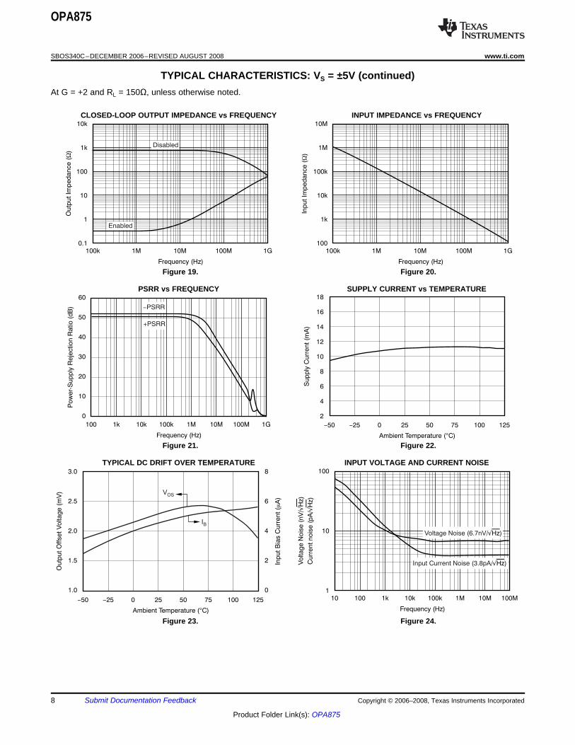
TYPICAL CHARACTERISTICS: VS = ±5V (continued)At G = +2 and RL = 150Ω, unless otherwise noted.
CLOSED-LOOP OUTPUT IMPEDANCE vs FREQUENCY INPUT IMPEDANCE vs FREQUENCY
Figure 19. Figure 20.
PSRR vs FREQUENCY SUPPLY CURRENT vs TEMPERATURE
Figure 21. Figure 22.
TYPICAL DC DRIFT OVER TEMPERATURE INPUT VOLTAGE AND CURRENT NOISE
Figure 23. Figure 24.
8 Submit Documentation Feedback Copyright © 2006–2008, Texas Instruments Incorporated
Product Folder Link(s): OPA875
APPLICATIONS INFORMATION
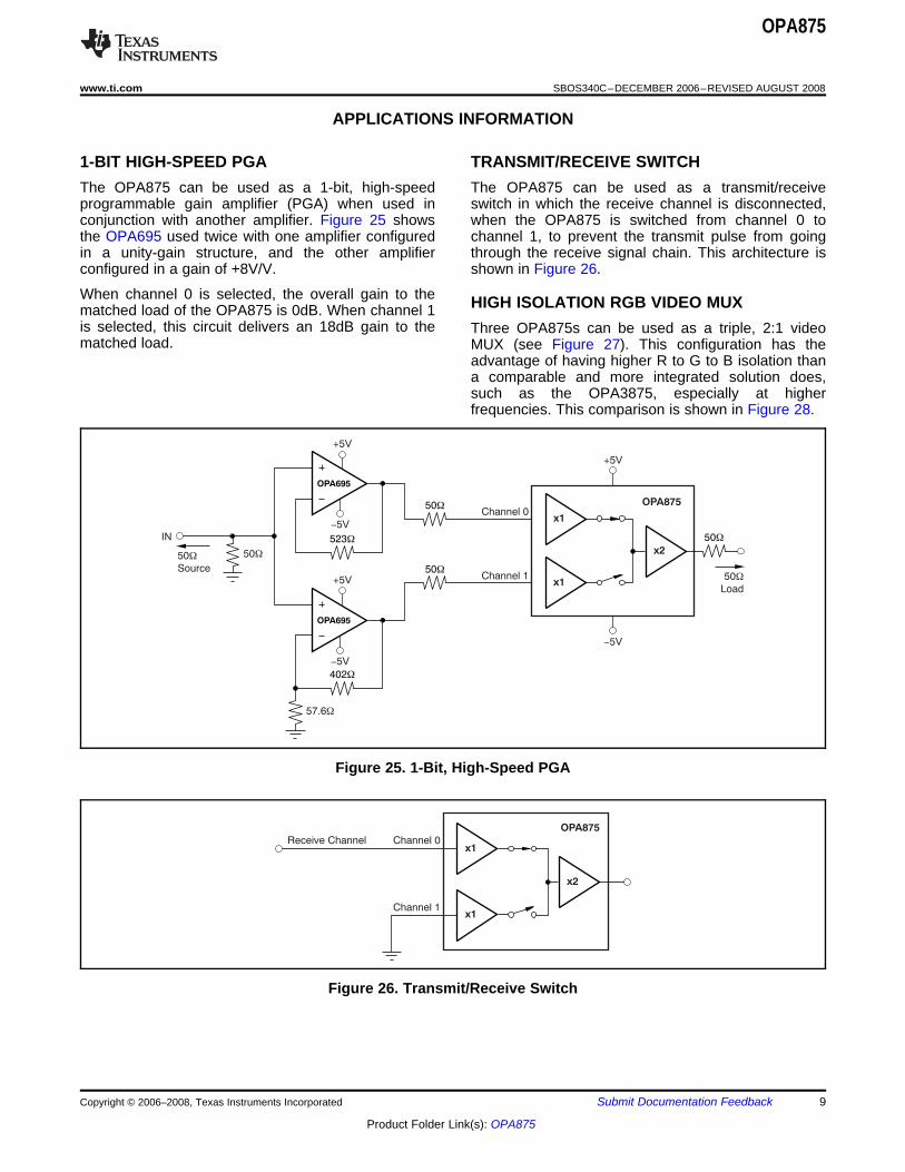
1-BIT HIGH-SPEED PGA TRANSMIT/RECEIVE SWITCH
HIGH ISOLATION RGB VIDEO MUX
50W
57.6W
50W
OPA875
x1
x2
x1
IN
50W
Source50W
Load
50W
50W
OPA695
Channel 0
Channel 1
523W
OPA695
402W
+5V
+5V
-5V
-5V
+5V
-5V
OPA875
x1
x2
x1
Receive Channel Channel 0
Channel 1
OPA875
www.ti.com ............................................................................................................................................ SBOS340C–DECEMBER 2006–REVISED AUGUST 2008
The OPA875 can be used as a 1-bit, high-speed The OPA875 can be used as a transmit/receiveprogrammable gain amplifier (PGA) when used in switch in which the receive channel is disconnected,conjunction with another amplifier. Figure 25 shows when the OPA875 is switched from channel 0 tothe OPA695 used twice with one amplifier configured channel 1, to prevent the transmit pulse from goingin a unity-gain structure, and the other amplifier through the receive signal chain. This architecture isconfigured in a gain of +8V/V. shown in Figure 26.
When channel 0 is selected, the overall gain to thematched load of the OPA875 is 0dB. When channel 1is selected, this circuit delivers an 18dB gain to the Three OPA875s can be used as a triple, 2:1 videomatched load. MUX (see Figure 27). This configuration has the
advantage of having higher R to G to B isolation thana comparable and more integrated solution does,such as the OPA3875, especially at higherfrequencies. This comparison is shown in Figure 28.
Figure 25. 1-Bit, High-Speed PGA
Figure 26. Transmit/Receive Switch
Copyright © 2006–2008, Texas Instruments Incorporated Submit Documentation Feedback 9
Product Folder Link(s): OPA875
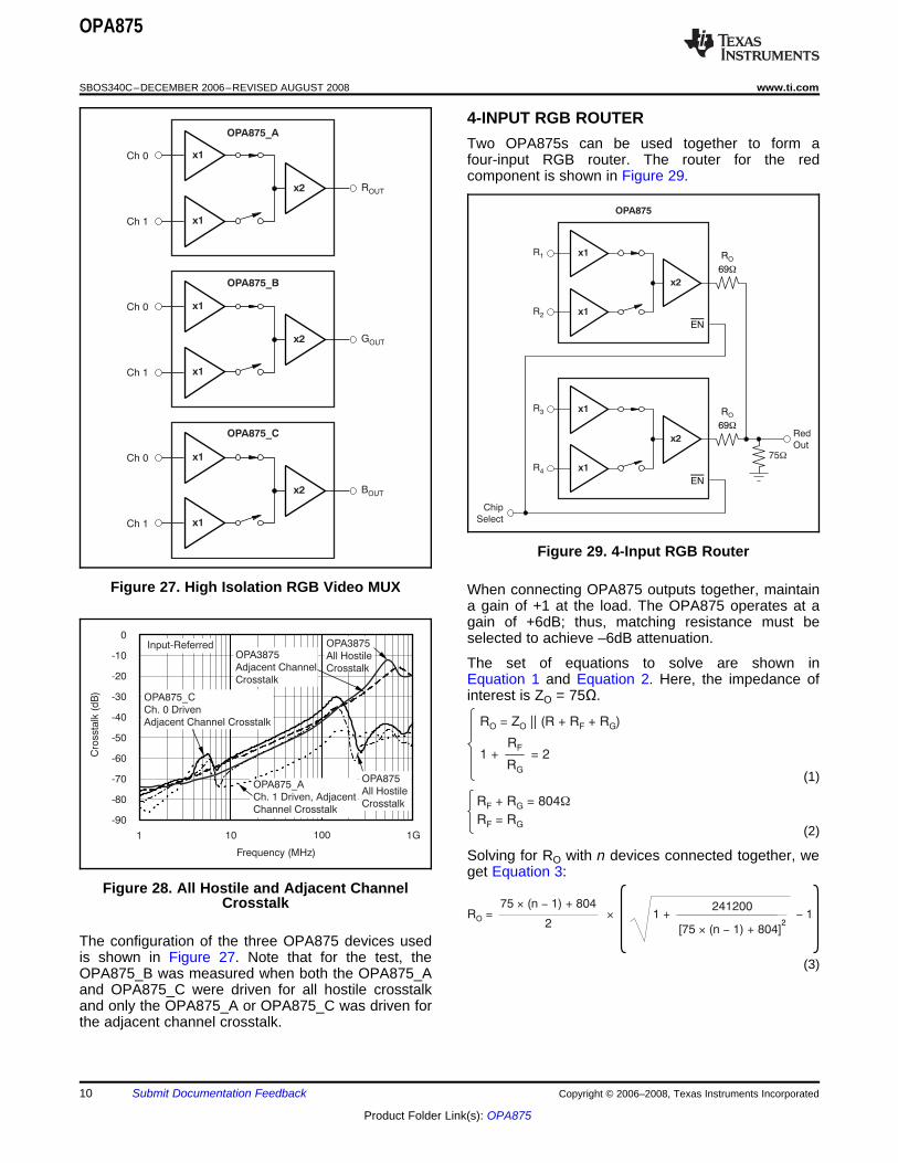
4-INPUT RGB ROUTER
R
69W
O
OPA875
x1
x2
x1
R1
R2
EN
R
69W
Ox1
x2
x1
R3
Chip
Select
Red
Out
R4
EN
75W
x1
x2
x1
ROUT
x1
x2
x1
GOUT
x1
x2
x1
BOUT
OPA875_A
OPA875_B
OPA875_C
Ch 0
Ch 1
Ch 0
Ch 1
Ch 0
Ch 1
R = Z || (R + R + R )O F GO
1 + = 2RF
RG (1)
R + R = 804
R = R
WF G
F G (2)
OPA875_A
Ch. 1 Driven, Adjacent
Channel Crosstalk
0
-10
-20
-30
-40
-50
-60
-70
-80
-90
Cro
ssta
lk (
dB
)
1 10 100 1G
Frequency (MHz)
Input-ReferredOPA3875
Adjacent Channel
Crosstalk
OPA3875
All Hostile
Crosstalk
OPA875
All Hostile
Crosstalk
OPA875_C
Ch. 0 Driven
Adjacent Channel Crosstalk
R =O2
75 (n 1) + 804´ -
´ 1 +
[75 (n 1) + 804]´ -2
241200- 1
OPA875
SBOS340C–DECEMBER 2006–REVISED AUGUST 2008 ............................................................................................................................................ www.ti.com
Two OPA875s can be used together to form afour-input RGB router. The router for the redcomponent is shown in Figure 29.
Figure 29. 4-Input RGB Router
Figure 27. High Isolation RGB Video MUX When connecting OPA875 outputs together, maintaina gain of +1 at the load. The OPA875 operates at again of +6dB; thus, matching resistance must beselected to achieve –6dB attenuation.
The set of equations to solve are shown inEquation 1 and Equation 2. Here, the impedance ofinterest is ZO = 75Ω.
Solving for RO with n devices connected together, weget Equation 3:
Figure 28. All Hostile and Adjacent ChannelCrosstalk
The configuration of the three OPA875 devices usedis shown in Figure 27. Note that for the test, the (3)OPA875_B was measured when both the OPA875_Aand OPA875_C were driven for all hostile crosstalkand only the OPA875_A or OPA875_C was driven forthe adjacent channel crosstalk.
10 Submit Documentation Feedback Copyright © 2006–2008, Texas Instruments Incorporated
Product Folder Link(s): OPA875
OPERATING SUGGESTIONS
DRIVING CAPACITIVE LOADS
DESIGN-IN TOOLS
DEMONSTRATION FIXTURES
MACROMODELS AND APPLICATIONS
DC ACCURACY
OPA875
www.ti.com ............................................................................................................................................ SBOS340C–DECEMBER 2006–REVISED AUGUST 2008
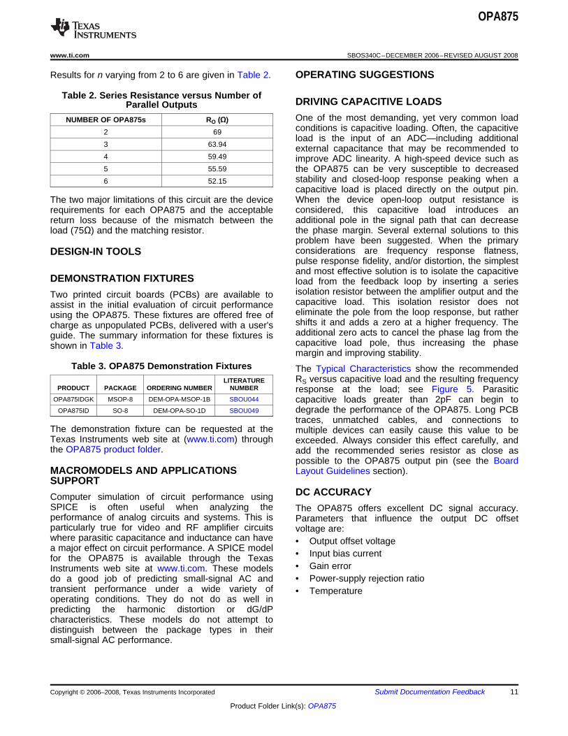
Results for n varying from 2 to 6 are given in Table 2.
Table 2. Series Resistance versus Number ofParallel Outputs
One of the most demanding, yet very common loadNUMBER OF OPA875s RO (Ω)conditions is capacitive loading. Often, the capacitive2 69load is the input of an ADC—including additional
3 63.94 external capacitance that may be recommended to4 59.49 improve ADC linearity. A high-speed device such as5 55.59 the OPA875 can be very susceptible to decreased
stability and closed-loop response peaking when a6 52.15capacitive load is placed directly on the output pin.When the device open-loop output resistance isThe two major limitations of this circuit are the deviceconsidered, this capacitive load introduces anrequirements for each OPA875 and the acceptableadditional pole in the signal path that can decreasereturn loss because of the mismatch between thethe phase margin. Several external solutions to thisload (75Ω) and the matching resistor.problem have been suggested. When the primaryconsiderations are frequency response flatness,pulse response fidelity, and/or distortion, the simplestand most effective solution is to isolate the capacitiveload from the feedback loop by inserting a seriesisolation resistor between the amplifier output and theTwo printed circuit boards (PCBs) are available tocapacitive load. This isolation resistor does notassist in the initial evaluation of circuit performanceeliminate the pole from the loop response, but ratherusing the OPA875. These fixtures are offered free ofshifts it and adds a zero at a higher frequency. Thecharge as unpopulated PCBs, delivered with a user'sadditional zero acts to cancel the phase lag from theguide. The summary information for these fixtures iscapacitive load pole, thus increasing the phaseshown in Table 3.margin and improving stability.
Table 3. OPA875 Demonstration Fixtures The Typical Characteristics show the recommendedRS versus capacitive load and the resulting frequencyLITERATURE
PRODUCT PACKAGE ORDERING NUMBER NUMBER response at the load; see Figure 5. ParasiticOPA875IDGK MSOP-8 DEM-OPA-MSOP-1B SBOU044 capacitive loads greater than 2pF can begin to
degrade the performance of the OPA875. Long PCBOPA875ID SO-8 DEM-OPA-SO-1D SBOU049traces, unmatched cables, and connections to
The demonstration fixture can be requested at the multiple devices can easily cause this value to beTexas Instruments web site at (www.ti.com) through exceeded. Always consider this effect carefully, andthe OPA875 product folder. add the recommended series resistor as close as
possible to the OPA875 output pin (see the BoardLayout Guidelines section).
SUPPORTComputer simulation of circuit performance usingSPICE is often useful when analyzing the The OPA875 offers excellent DC signal accuracy.performance of analog circuits and systems. This is Parameters that influence the output DC offsetparticularly true for video and RF amplifier circuits voltage are:where parasitic capacitance and inductance can have • Output offset voltagea major effect on circuit performance. A SPICE model • Input bias currentfor the OPA875 is available through the Texas
• Gain errorInstruments web site at www.ti.com. These models• Power-supply rejection ratiodo a good job of predicting small-signal AC and
transient performance under a wide variety of • Temperatureoperating conditions. They do not do as well inpredicting the harmonic distortion or dG/dPcharacteristics. These models do not attempt todistinguish between the package types in theirsmall-signal AC performance.
Copyright © 2006–2008, Texas Instruments Incorporated Submit Documentation Feedback 11
Product Folder Link(s): OPA875
V = V + (R I ) x G 5 (V ) x 10± | |OSO_envelope OSO S b S+-·-
PSRR+20
PSRR-
20± | |5 (V ) x 10S-- -
-
NOISE PERFORMANCE
± ± ±14mV + 75 xW 18 A x 2m | |5 6 x 10-
5020
-
5120
-
± 5 ( 6) x 10| |-- -
= ±22.7mV (5)
DISTORTION PERFORMANCE
+5V
-5V Channel
Select
EN
OPA875
+1
+2
+1
en
ibRS
eRS
eO
e = 2o e + (i R ) + 4kTRn b S S
2 2
(6)
OPA875
SBOS340C–DECEMBER 2006–REVISED AUGUST 2008 ............................................................................................................................................ www.ti.com
Leaving both temperature and gain error parameters output stage continues to hold them low even as theaside, the output offset voltage envelope can be fundamental power reaches very high levels. As thedescribed as shown in Equation 4: Typical Characteristics show, the spurious
intermodulation powers do not increase as predictedby a traditional intercept model. As the fundamentalpower level increases, the dynamic range does notdecrease significantly. For two tones centered at
(4) 20MHz, with 4dBm/tone into a matched 50Ω load(that is, 1VPP for each tone at the load, which requiresWith:4VPP for the overall 2-tone envelope at the outputVOSO: Output offset voltage pin), the Typical Characteristics show a 82dBc
RS: Input resistance seen by R0, R1, G0, G1, B0, difference between the test-tone power and theor B1. 3rd-order intermodulation spurious levels.Ib: Input bias currentG: GainVS+: Positive supply voltage The OPA875 offers an excellent balance between
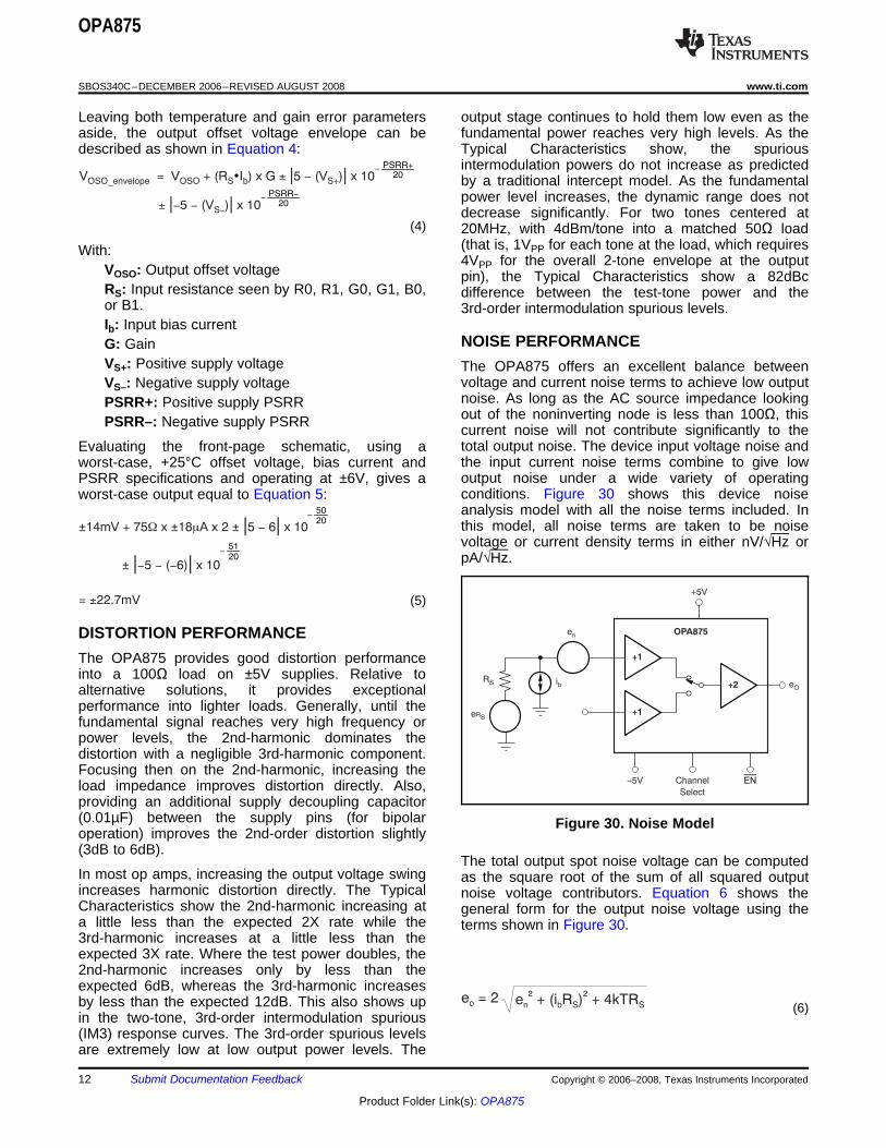
voltage and current noise terms to achieve low outputVS–: Negative supply voltagenoise. As long as the AC source impedance lookingPSRR+: Positive supply PSRRout of the noninverting node is less than 100Ω, thisPSRR–: Negative supply PSRR current noise will not contribute significantly to thetotal output noise. The device input voltage noise andEvaluating the front-page schematic, using athe input current noise terms combine to give lowworst-case, +25°C offset voltage, bias current andoutput noise under a wide variety of operatingPSRR specifications and operating at ±6V, gives aconditions. Figure 30 shows this device noiseworst-case output equal to Equation 5:analysis model with all the noise terms included. Inthis model, all noise terms are taken to be noisevoltage or current density terms in either nV/√Hz orpA/√Hz.
The OPA875 provides good distortion performanceinto a 100Ω load on ±5V supplies. Relative toalternative solutions, it provides exceptionalperformance into lighter loads. Generally, until thefundamental signal reaches very high frequency orpower levels, the 2nd-harmonic dominates thedistortion with a negligible 3rd-harmonic component.Focusing then on the 2nd-harmonic, increasing theload impedance improves distortion directly. Also,providing an additional supply decoupling capacitor(0.01µF) between the supply pins (for bipolar Figure 30. Noise Modeloperation) improves the 2nd-order distortion slightly(3dB to 6dB).
The total output spot noise voltage can be computedIn most op amps, increasing the output voltage swing as the square root of the sum of all squared outputincreases harmonic distortion directly. The Typical noise voltage contributors. Equation 6 shows theCharacteristics show the 2nd-harmonic increasing at general form for the output noise voltage using thea little less than the expected 2X rate while the terms shown in Figure 30.3rd-harmonic increases at a little less than theexpected 3X rate. Where the test power doubles, the2nd-harmonic increases only by less than theexpected 6dB, whereas the 3rd-harmonic increasesby less than the expected 12dB. This also shows upin the two-tone, 3rd-order intermodulation spurious(IM3) response curves. The 3rd-order spurious levelsare extremely low at low output power levels. The
12 Submit Documentation Feedback Copyright © 2006–2008, Texas Instruments Incorporated
Product Folder Link(s): OPA875
BOARD LAYOUT GUIDELINES
e =n e + (i R ) + 4kTRn Sb S
2 2
(7)
THERMAL ANALYSIS
P = 10V x 11mA + (5 [4 x (100 || 804 ) ] ) = 180mWD W W2
Maximum T = +85 C + (0.18mW x 140°C/W) = 110°CJ °
OPA875
www.ti.com ............................................................................................................................................ SBOS340C–DECEMBER 2006–REVISED AUGUST 2008
Dividing this expression by the device gain (2V/V)gives the equivalent input-referred spot noise voltage Achieving optimum performance with a highat the noninverting input as shown in Equation 7. frequency amplifier such as the OPA875 requires
careful attention to board layout parasitics andexternal component types. Recommendations thatwill optimize performance include:Evaluating these two equations for the OPA875
circuit and component values shown in Figure 30 a) Minimize parasitic capacitance to any ACgives a total output spot noise voltage of 13.6nV/√Hz ground for all of the signal I/O pins. Parasiticand a total equivalent input spot noise voltage of capacitance on the output pin can cause instability:6.8nV/√Hz. This total input-referred spot noise on the noninverting input, it can react with the sourcevoltage is higher than the 6.7nV/√Hz specification for impedance to cause unintentional bandlimiting. Tothe mux voltage noise alone. This number reflects the reduce unwanted capacitance, a window around thenoise added to the output by the bias current noise signal I/O pins should be opened in all of the groundtimes the source resistor. and power planes around those pins. Otherwise,ground and power planes should be unbrokenelsewhere on the board.
Heatsinking or forced airflow may be required under b) Minimize the distance (< 0.25") from theextreme operating conditions. Maximum desired power-supply pins to high frequency 0.1µFjunction temperature will set the maximum allowed decoupling capacitors. At the device pins, theinternal power dissipation as discussed in this ground and power plane layout should not be in closedocument. In no case should the maximum junction proximity to the signal I/O pins. Avoid narrow powertemperature be allowed to exceed +150°C. and ground traces to minimize inductance between
the pins and the decoupling capacitors. TheOperating junction temperature (TJ) is given by TA +power-supply connections (on pins 9, 11, 13, and 15)PD × θJA. The total internal power dissipation (PD) isshould always be decoupled with these capacitors.the sum of quiescent power (PDQ) and additionalAn optional supply decoupling capacitor across thepower dissipated in the output stage (PDL) to delivertwo power supplies (for bipolar operation) will improveload power. Quiescent power is simply the specified2nd-harmonic distortion performance. Larger (2.2µFno-load supply current times the total supply voltageto 6.8µF) decoupling capacitors, effective at loweracross the part. PDL depends on the required outputfrequency, should also be used on the main supplysignal and load but, for a grounded resistive load, bepins. These may be placed somewhat farther fromat a maximum when the output is fixed at a voltagethe device and may be shared among severalequal to 1/2 of either supply voltage (for equal bipolardevices in the same area of the PCB.supplies). Under this condition PDL = VS
2/(4 × RL),where RL includes feedback network loading. c) Careful selection and placement of external
components will preserve the high-frequencyNote that it is the power in the output stage and not inperformance of the OPA875. Resistors should be athe load that determines internal power dissipation.very low reactance type. Surface-mount resistors
As a worst-case example, compute the maximum TJ work best and allow a tighter overall layout. Metal-filmusing an OPA875IDGK in the circuit of Figure 30 and carbon composition, axially leaded resistors canoperating at the maximum specified ambient also provide good high-frequency performance.temperature of +85°C with its outputs driving a Again, keep the leads and PCB trace length as shortgrounded 100Ω load to +2.5V: as possible. Never use wirewound type resistors in a
high-frequency application. Other networkcomponents, such as noninverting input terminationresistors, should also be placed close to the package.
This worst-case condition does not exceed the d) Connections to other wideband devices on themaximum junction temperature. Normally, this board may be made with short direct traces orextreme case is not encountered. Careful attention to through onboard transmission lines. For shortinternal power dissipation is required. connections, consider the trace and the input to the
next device as a lumped capacitive load. Relativelywide traces (50mils to 100mils) should be used,preferably with ground and power planes opened uparound them.
Copyright © 2006–2008, Texas Instruments Incorporated Submit Documentation Feedback 13
Product Folder Link(s): OPA875
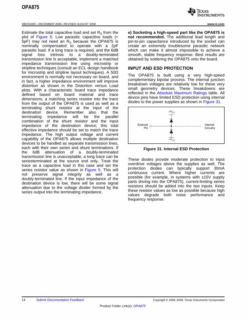
INPUT AND ESD PROTECTION
ExternalPin
+VCC
-VCC
InternalCircuitry
OPA875
SBOS340C–DECEMBER 2006–REVISED AUGUST 2008 ............................................................................................................................................ www.ti.com
Estimate the total capacitive load and set RS from the e) Socketing a high-speed part like the OPA875 isplot of Figure 5. Low parasitic capacitive loads (< not recommended. The additional lead length and5pF) may not need an RS because the OPA875 is pin-to-pin capacitance introduced by the socket cannominally compensated to operate with a 2pF create an extremely troublesome parasitic networkparasitic load. If a long trace is required, and the 6dB which can make it almost impossible to achieve asignal loss intrinsic to a doubly-terminated smooth, stable frequency response. Best results aretransmission line is acceptable, implement a matched obtained by soldering the OPA875 onto the board.impedance transmission line using microstrip orstripline techniques (consult an ECL design handbookfor microstrip and stripline layout techniques). A 50Ω
The OPA875 is built using a very high-speedenvironment is normally not necessary on board, andcomplementary bipolar process. The internal junctionin fact, a higher impedance environment will improvebreakdown voltages are relatively low for these verydistortion as shown in the Distortion versus Loadsmall geometry devices. These breakdowns areplots. With a characteristic board trace impedancereflected in the Absolute Maximum Ratings table. Alldefined based on board material and tracedevice pins have limited ESD protection using internaldimensions, a matching series resistor into the tracediodes to the power supplies as shown in Figure 31.from the output of the OPA875 is used as well as a
terminating shunt resistor at the input of thedestination device. Remember also that theterminating impedance will be the parallelcombination of the shunt resistor and the inputimpedance of the destination device; this totaleffective impedance should be set to match the traceimpedance. The high output voltage and currentcapability of the OPA875 allows multiple destinationdevices to be handled as separate transmission lines,each with their own series and shunt terminations. If Figure 31. Internal ESD Protectionthe 6dB attenuation of a doubly-terminatedtransmission line is unacceptable, a long trace can be
These diodes provide moderate protection to inputseriesterminated at the source end only. Treat theoverdrive voltages above the supplies as well. Thetrace as a capacitive load in this case and set theprotection diodes can typically support 30mAseries resistor value as shown in Figure 5. This willcontinuous current. Where higher currents arenot preserve signal integrity as well as apossible (for example, in systems with ±15V supplydoubly-terminated line. If the input impedance of theparts driving into the OPA875), current-limiting seriesdestination device is low, there will be some signalresistors should be added into the two inputs. Keepattenuation due to the voltage divider formed by thethese resistor values as low as possible because highseries output into the terminating impedance.values degrade both noise performance andfrequency response.
14 Submit Documentation Feedback Copyright © 2006–2008, Texas Instruments Incorporated
Product Folder Link(s): OPA875
OPA875
www.ti.com ............................................................................................................................................ SBOS340C–DECEMBER 2006–REVISED AUGUST 2008
Revision History
Changes from Revision B (September 2007) to Revision C .......................................................................................... Page
• Changed storage temperature range rating in Absolute Maximum Ratings table from –40°C to +125°C to –65°C to+125°C................................................................................................................................................................................... 2
Changes from Revision A (August 2007) to Revision B ................................................................................................ Page
• Changed ordering information column in Table 3................................................................................................................ 11
Copyright © 2006–2008, Texas Instruments Incorporated Submit Documentation Feedback 15
Product Folder Link(s): OPA875
PACKAGE OPTION ADDENDUM
www.ti.com 13-Aug-2021
Addendum-Page 1
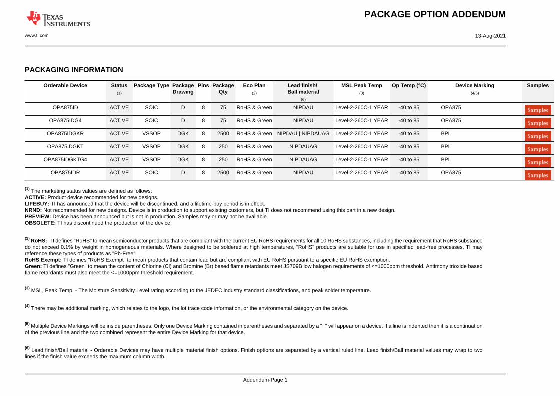
PACKAGING INFORMATION
Orderable Device Status(1)
Package Type PackageDrawing
Pins PackageQty
Eco Plan(2)
Lead finish/Ball material
(6)
MSL Peak Temp(3)
Op Temp (°C) Device Marking(4/5)
Samples
OPA875ID ACTIVE SOIC D 8 75 RoHS & Green NIPDAU Level-2-260C-1 YEAR -40 to 85 OPA875
OPA875IDG4 ACTIVE SOIC D 8 75 RoHS & Green NIPDAU Level-2-260C-1 YEAR -40 to 85 OPA875
OPA875IDGKR ACTIVE VSSOP DGK 8 2500 RoHS & Green NIPDAU | NIPDAUAG Level-2-260C-1 YEAR -40 to 85 BPL
OPA875IDGKT ACTIVE VSSOP DGK 8 250 RoHS & Green NIPDAUAG Level-2-260C-1 YEAR -40 to 85 BPL
OPA875IDGKTG4 ACTIVE VSSOP DGK 8 250 RoHS & Green NIPDAUAG Level-2-260C-1 YEAR -40 to 85 BPL
OPA875IDR ACTIVE SOIC D 8 2500 RoHS & Green NIPDAU Level-2-260C-1 YEAR -40 to 85 OPA875
(1) The marketing status values are defined as follows:ACTIVE: Product device recommended for new designs.LIFEBUY: TI has announced that the device will be discontinued, and a lifetime-buy period is in effect.NRND: Not recommended for new designs. Device is in production to support existing customers, but TI does not recommend using this part in a new design.PREVIEW: Device has been announced but is not in production. Samples may or may not be available.OBSOLETE: TI has discontinued the production of the device.
(2) RoHS: TI defines "RoHS" to mean semiconductor products that are compliant with the current EU RoHS requirements for all 10 RoHS substances, including the requirement that RoHS substancedo not exceed 0.1% by weight in homogeneous materials. Where designed to be soldered at high temperatures, "RoHS" products are suitable for use in specified lead-free processes. TI mayreference these types of products as "Pb-Free".RoHS Exempt: TI defines "RoHS Exempt" to mean products that contain lead but are compliant with EU RoHS pursuant to a specific EU RoHS exemption.Green: TI defines "Green" to mean the content of Chlorine (Cl) and Bromine (Br) based flame retardants meet JS709B low halogen requirements of <=1000ppm threshold. Antimony trioxide basedflame retardants must also meet the <=1000ppm threshold requirement.
(3) MSL, Peak Temp. - The Moisture Sensitivity Level rating according to the JEDEC industry standard classifications, and peak solder temperature.
(4) There may be additional marking, which relates to the logo, the lot trace code information, or the environmental category on the device.
(5) Multiple Device Markings will be inside parentheses. Only one Device Marking contained in parentheses and separated by a "~" will appear on a device. If a line is indented then it is a continuationof the previous line and the two combined represent the entire Device Marking for that device.
(6) Lead finish/Ball material - Orderable Devices may have multiple material finish options. Finish options are separated by a vertical ruled line. Lead finish/Ball material values may wrap to twolines if the finish value exceeds the maximum column width.
PACKAGE OPTION ADDENDUM
www.ti.com 13-Aug-2021
Addendum-Page 2
Important Information and Disclaimer:The information provided on this page represents TI's knowledge and belief as of the date that it is provided. TI bases its knowledge and belief on informationprovided by third parties, and makes no representation or warranty as to the accuracy of such information. Efforts are underway to better integrate information from third parties. TI has taken andcontinues to take reasonable steps to provide representative and accurate information but may not have conducted destructive testing or chemical analysis on incoming materials and chemicals.TI and TI suppliers consider certain information to be proprietary, and thus CAS numbers and other limited information may not be available for release.
In no event shall TI's liability arising out of such information exceed the total purchase price of the TI part(s) at issue in this document sold by TI to Customer on an annual basis.
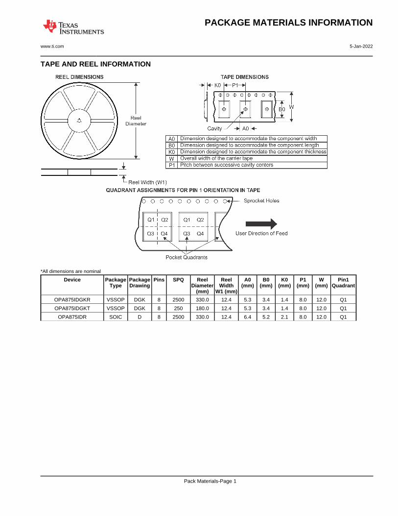
TAPE AND REEL INFORMATION
*All dimensions are nominal
Device PackageType
PackageDrawing
Pins SPQ ReelDiameter
(mm)
ReelWidth
W1 (mm)
A0(mm)
B0(mm)
K0(mm)
P1(mm)
W(mm)
Pin1Quadrant
OPA875IDGKR VSSOP DGK 8 2500 330.0 12.4 5.3 3.4 1.4 8.0 12.0 Q1
OPA875IDGKT VSSOP DGK 8 250 180.0 12.4 5.3 3.4 1.4 8.0 12.0 Q1
OPA875IDR SOIC D 8 2500 330.0 12.4 6.4 5.2 2.1 8.0 12.0 Q1
PACKAGE MATERIALS INFORMATION
www.ti.com 5-Jan-2022
Pack Materials-Page 1
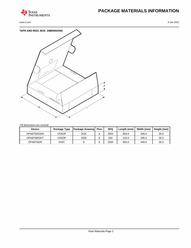
*All dimensions are nominal
Device Package Type Package Drawing Pins SPQ Length (mm) Width (mm) Height (mm)
OPA875IDGKR VSSOP DGK 8 2500 853.0 449.0 35.0
OPA875IDGKT VSSOP DGK 8 250 210.0 185.0 35.0
OPA875IDR SOIC D 8 2500 853.0 449.0 35.0
PACKAGE MATERIALS INFORMATION
www.ti.com 5-Jan-2022
Pack Materials-Page 2
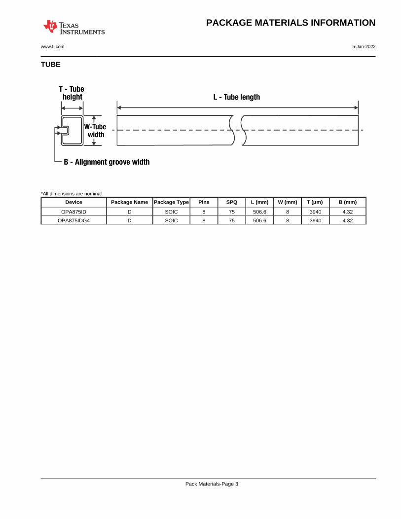
TUBE
*All dimensions are nominal
Device Package Name Package Type Pins SPQ L (mm) W (mm) T (µm) B (mm)
OPA875ID D SOIC 8 75 506.6 8 3940 4.32
OPA875IDG4 D SOIC 8 75 506.6 8 3940 4.32
PACKAGE MATERIALS INFORMATION
www.ti.com 5-Jan-2022
Pack Materials-Page 3
www.ti.com
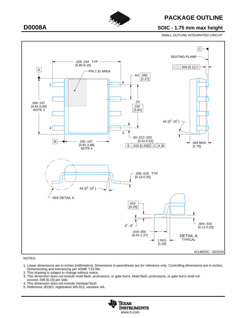
PACKAGE OUTLINE
C
.228-.244 TYP[5.80-6.19]
.069 MAX[1.75]
6X .050[1.27]
8X .012-.020 [0.31-0.51]
2X.150[3.81]
.005-.010 TYP[0.13-0.25]
0 - 8 .004-.010[0.11-0.25]
.010[0.25]
.016-.050[0.41-1.27]
4X (0 -15 )
A
.189-.197[4.81-5.00]
NOTE 3
B .150-.157[3.81-3.98]
NOTE 4
4X (0 -15 )
(.041)[1.04]
SOIC - 1.75 mm max heightD0008ASMALL OUTLINE INTEGRATED CIRCUIT
4214825/C 02/2019
NOTES: 1. Linear dimensions are in inches [millimeters]. Dimensions in parenthesis are for reference only. Controlling dimensions are in inches. Dimensioning and tolerancing per ASME Y14.5M. 2. This drawing is subject to change without notice. 3. This dimension does not include mold flash, protrusions, or gate burrs. Mold flash, protrusions, or gate burrs shall not exceed .006 [0.15] per side. 4. This dimension does not include interlead flash.5. Reference JEDEC registration MS-012, variation AA.
18
.010 [0.25] C A B
54
PIN 1 ID AREA
SEATING PLANE
.004 [0.1] C
SEE DETAIL A
DETAIL ATYPICAL
SCALE 2.800
www.ti.com
EXAMPLE BOARD LAYOUT
.0028 MAX[0.07]ALL AROUND
.0028 MIN[0.07]ALL AROUND
(.213)[5.4]
6X (.050 )[1.27]
8X (.061 )[1.55]
8X (.024)[0.6]
(R.002 ) TYP[0.05]
SOIC - 1.75 mm max heightD0008ASMALL OUTLINE INTEGRATED CIRCUIT
4214825/C 02/2019
NOTES: (continued) 6. Publication IPC-7351 may have alternate designs. 7. Solder mask tolerances between and around signal pads can vary based on board fabrication site.
METALSOLDER MASKOPENING
NON SOLDER MASKDEFINED
SOLDER MASK DETAILS
EXPOSEDMETAL
OPENINGSOLDER MASK METAL UNDER
SOLDER MASK
SOLDER MASKDEFINED
EXPOSEDMETAL
LAND PATTERN EXAMPLEEXPOSED METAL SHOWN
SCALE:8X
SYMM
1
45
8
SEEDETAILS
SYMM
www.ti.com
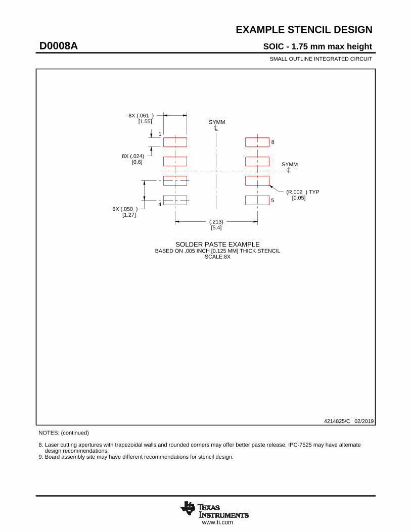
EXAMPLE STENCIL DESIGN
8X (.061 )[1.55]
8X (.024)[0.6]
6X (.050 )[1.27]
(.213)[5.4]
(R.002 ) TYP[0.05]
SOIC - 1.75 mm max heightD0008ASMALL OUTLINE INTEGRATED CIRCUIT
4214825/C 02/2019
NOTES: (continued) 8. Laser cutting apertures with trapezoidal walls and rounded corners may offer better paste release. IPC-7525 may have alternate design recommendations. 9. Board assembly site may have different recommendations for stencil design.
SOLDER PASTE EXAMPLEBASED ON .005 INCH [0.125 MM] THICK STENCIL
SCALE:8X
SYMM
SYMM
1
45
8

IMPORTANT NOTICE AND DISCLAIMERTI PROVIDES TECHNICAL AND RELIABILITY DATA (INCLUDING DATA SHEETS), DESIGN RESOURCES (INCLUDING REFERENCE DESIGNS), APPLICATION OR OTHER DESIGN ADVICE, WEB TOOLS, SAFETY INFORMATION, AND OTHER RESOURCES “AS IS” AND WITH ALL FAULTS, AND DISCLAIMS ALL WARRANTIES, EXPRESS AND IMPLIED, INCLUDING WITHOUT LIMITATION ANY IMPLIED WARRANTIES OF MERCHANTABILITY, FITNESS FOR A PARTICULAR PURPOSE OR NON-INFRINGEMENT OF THIRD PARTY INTELLECTUAL PROPERTY RIGHTS.These resources are intended for skilled developers designing with TI products. You are solely responsible for (1) selecting the appropriate TI products for your application, (2) designing, validating and testing your application, and (3) ensuring your application meets applicable standards, and any other safety, security, regulatory or other requirements.These resources are subject to change without notice. TI grants you permission to use these resources only for development of an application that uses the TI products described in the resource. Other reproduction and display of these resources is prohibited. No license is granted to any other TI intellectual property right or to any third party intellectual property right. TI disclaims responsibility for, and you will fully indemnify TI and its representatives against, any claims, damages, costs, losses, and liabilities arising out of your use of these resources.TI’s products are provided subject to TI’s Terms of Sale or other applicable terms available either on ti.com or provided in conjunction with such TI products. TI’s provision of these resources does not expand or otherwise alter TI’s applicable warranties or warranty disclaimers for TI products.TI objects to and rejects any additional or different terms you may have proposed. IMPORTANT NOTICE
Mailing Address: Texas Instruments, Post Office Box 655303, Dallas, Texas 75265Copyright © 2022, Texas Instruments Incorporated