Embed Size (px)
Citation preview
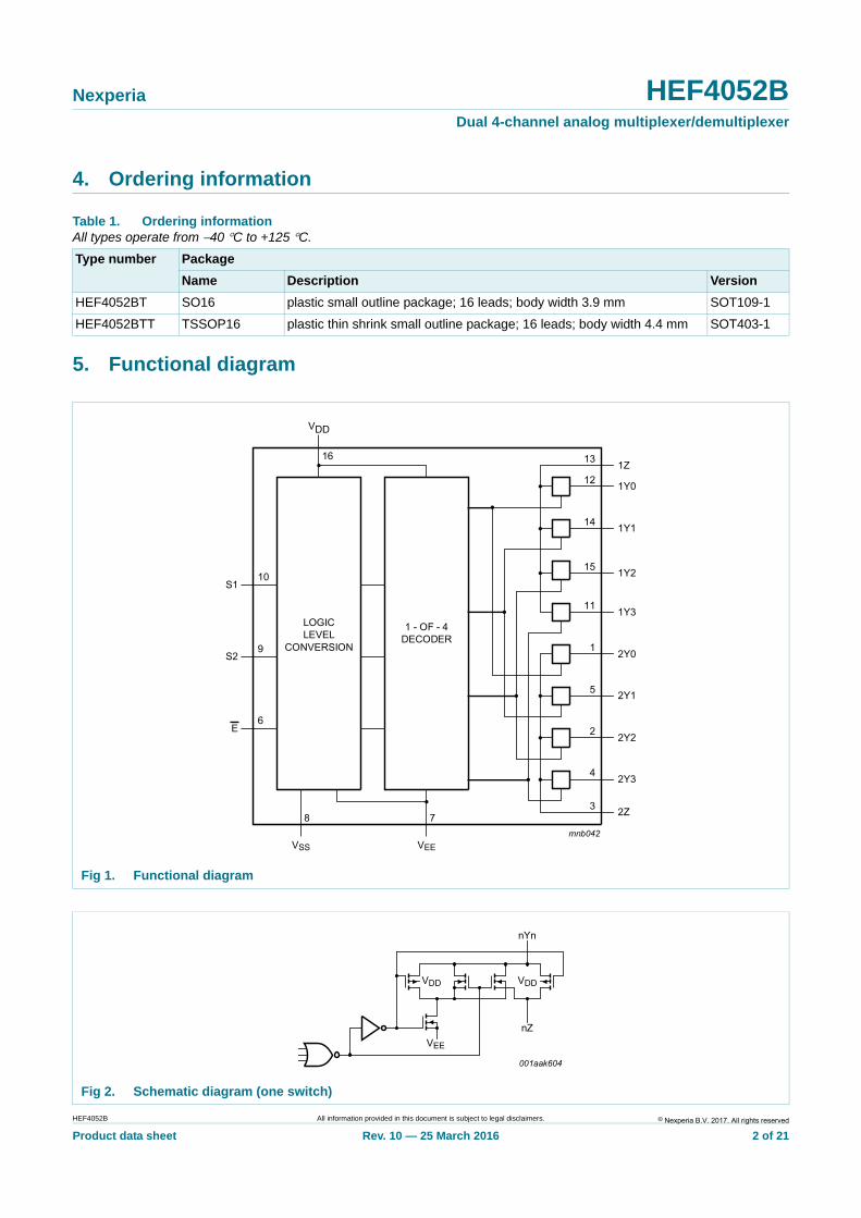
1. General description
The HEF4052B is a dual 4-channel analog multiplexer/demultiplexer with common channel select logic. Each multiplexer/demultiplexer has four independent inputs/outputs (nY0 to nY3) and a common input/output (nZ). The common channel select logic includes two select inputs (S1 and S2) and an active LOW enable input (E). Both multiplexers/demultiplexers contain four bidirectional analog switches, each with one side connected to an independent input/output (nY0 to nY3) and the other side connected to a common input/output (nZ). With E LOW, one of the four switches is selected (low-impedance ON-state) by S1 and S2. With E HIGH, all switches are in the high-impedance OFF-state, independent of S1 and S2. If break before make is needed, then it is necessary to use the enable input.
VDD and VSS are the supply voltage connections for the digital control inputs (S1 and S2, and E). The VDD to VSS range is 3 V to 15 V. The analog inputs/outputs (nY0 to nY3, and nZ) can swing between VDD as a positive limit and VEE as a negative limit. VDD VEE may not exceed 15 V. Unused inputs must be connected to VDD, VSS, or another input. For operation as a digital multiplexer/demultiplexer, VEE is connected to VSS (typically ground). VEE and VSS are the supply voltage connections for the switches.
2. Features and benefits
Fully static operation
5 V, 10 V, and 15 V parametric ratings
Standardized symmetrical output characteristics
Specified from 40 C to +85 C and 40 C to +125 C Complies with JEDEC standard JESD 13-B
3. Applications
Analog multiplexing and demultiplexing
Digital multiplexing and demultiplexing
Signal gating
HEF4052BDual 4-channel analog multiplexer/demultiplexerRev. 10 — 25 March 2016 Product data sheet
Nexperia HEF4052BDual 4-channel analog multiplexer/demultiplexer
4. Ordering information
5. Functional diagram
Table 1. Ordering informationAll types operate from 40 C to +125 C.
Type number Package
Name Description Version
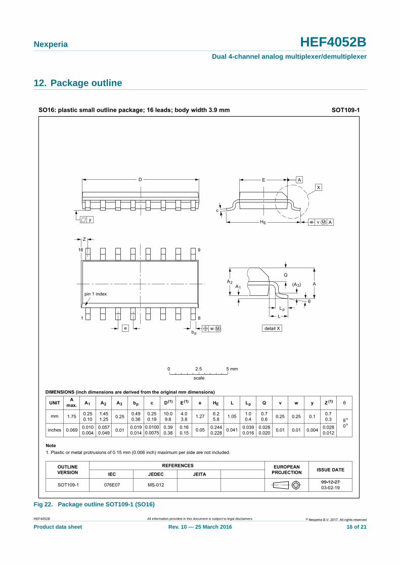
HEF4052BT SO16 plastic small outline package; 16 leads; body width 3.9 mm SOT109-1
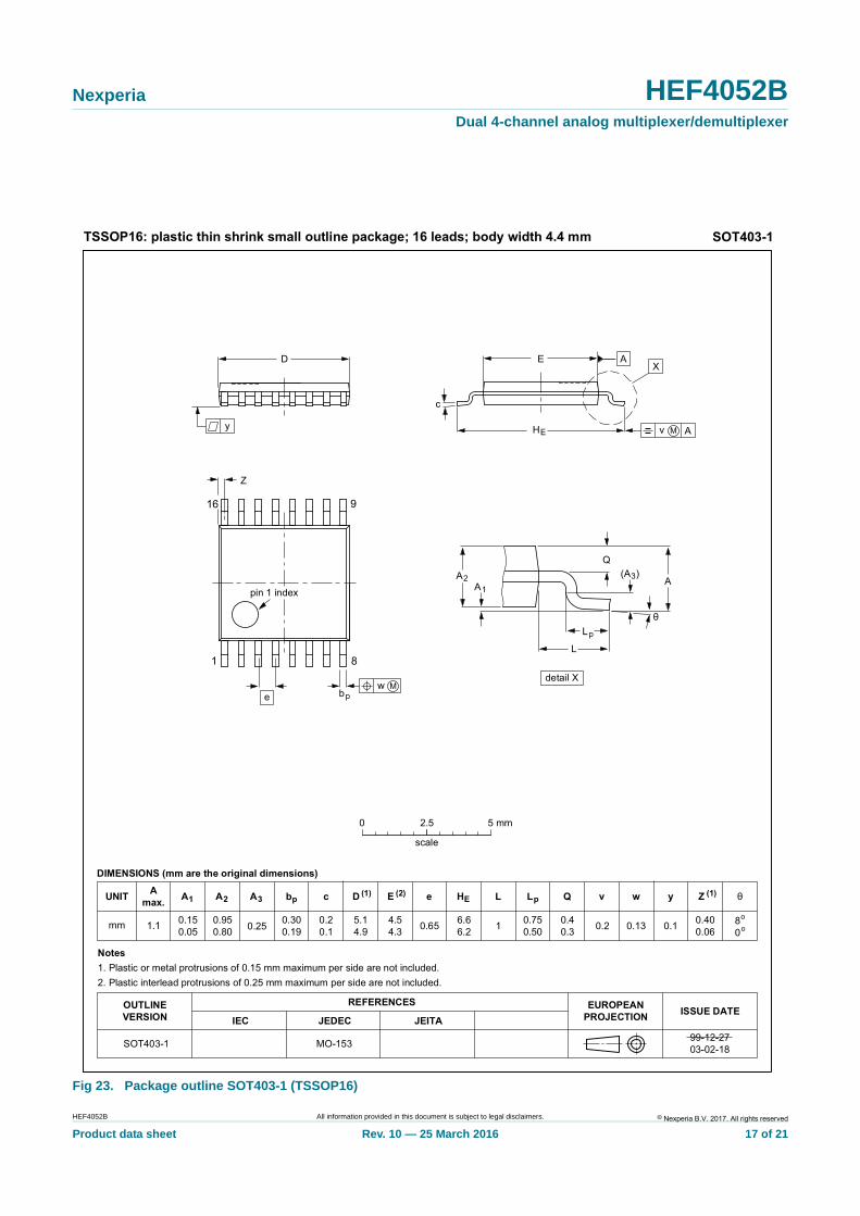
HEF4052BTT TSSOP16 plastic thin shrink small outline package; 16 leads; body width 4.4 mm SOT403-1
Fig 1. Functional diagram
Fig 2. Schematic diagram (one switch)
© Nexperia B.V. 2017. All rights reservedHEF4052B All information provided in this document is subject to legal disclaimers.
Product data sheet Rev. 10 — 25 March 2016 2 of 21
Nexperia HEF4052BDual 4-channel analog multiplexer/demultiplexer
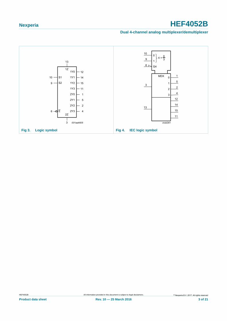
Fig 3. Logic symbol Fig 4. IEC logic symbol
© Nexperia B.V. 2017. All rights reservedHEF4052B All information provided in this document is subject to legal disclaimers.
Product data sheet Rev. 10 — 25 March 2016 3 of 21
Nexperia HEF4052BDual 4-channel analog multiplexer/demultiplexer
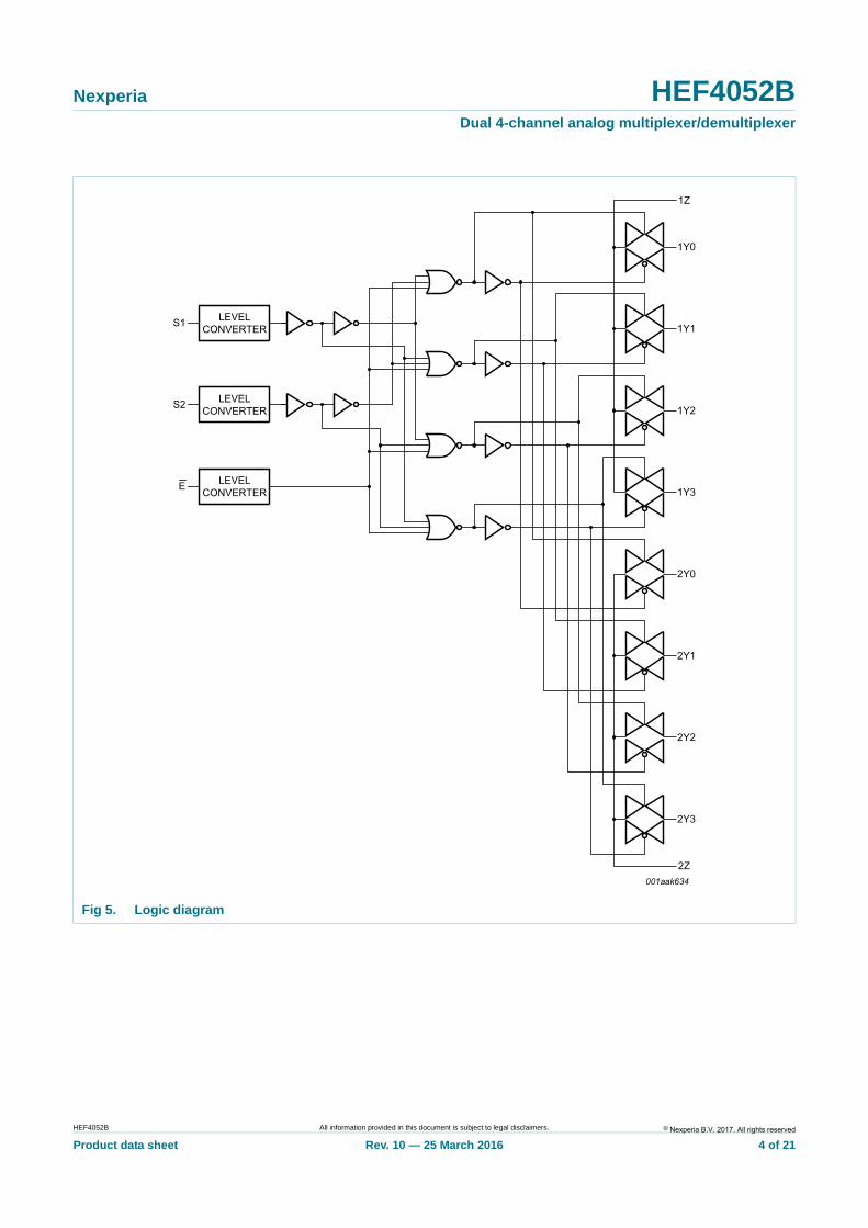
Fig 5. Logic diagram
© Nexperia B.V. 2017. All rights reservedHEF4052B All information provided in this document is subject to legal disclaimers.
Product data sheet Rev. 10 — 25 March 2016 4 of 21
Nexperia HEF4052BDual 4-channel analog multiplexer/demultiplexer
6. Pinning information
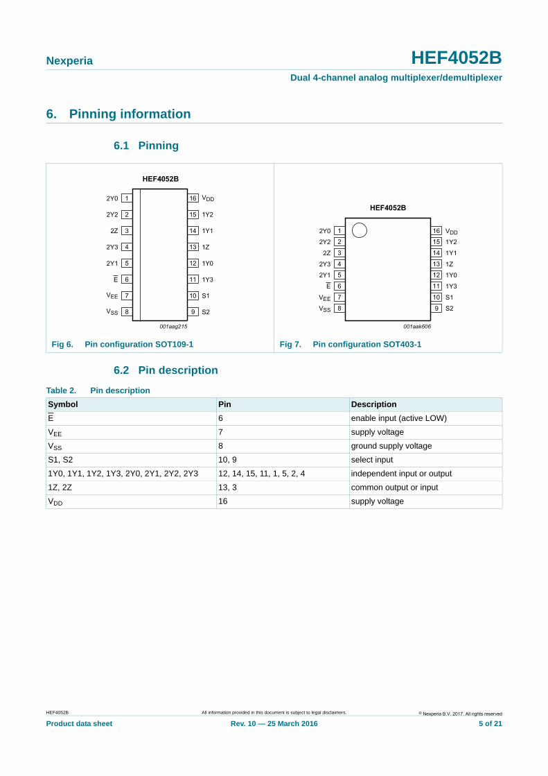
6.1 Pinning
6.2 Pin description
Fig 6. Pin configuration SOT109-1 Fig 7. Pin configuration SOT403-1
Table 2. Pin description
Symbol Pin Description
E 6 enable input (active LOW)
VEE 7 supply voltage
VSS 8 ground supply voltage
S1, S2 10, 9 select input
1Y0, 1Y1, 1Y2, 1Y3, 2Y0, 2Y1, 2Y2, 2Y3 12, 14, 15, 11, 1, 5, 2, 4 independent input or output
1Z, 2Z 13, 3 common output or input
VDD 16 supply voltage
© Nexperia B.V. 2017. All rights reservedHEF4052B All information provided in this document is subject to legal disclaimers.
Product data sheet Rev. 10 — 25 March 2016 5 of 21
Nexperia HEF4052BDual 4-channel analog multiplexer/demultiplexer
7. Functional description
7.1 Function table
[1] H = HIGH voltage level;
L = LOW voltage level;
X = don’t care.
8. Limiting values
[1] To avoid drawing VDD current out of terminal Z, when switch current flows into terminals Y, the voltage drop across the bidirectional switch must not exceed 0.4 V. If the switch current flows into terminal Z, no VDD current will flow out of terminals Y, and in this case there is no limit for the voltage drop across the switch, but the voltages at Y and Z may not exceed VDD or VEE.
[2] For SO16 package: Ptot derates linearly with 8 mW/K above 70 C.
For SSOP16 package: Ptot derates linearly with 5.5 mW/K above 60 C.
Table 3. Function table[1]
Input Channel on
E S2 S1
L L L nY0 to nZ
L L H nY1 to nZ
L H L nY2 to nZ
L H H nY3 to nZ
H X X switches off
Table 4. Limiting valuesIn accordance with the Absolute Maximum Rating System (IEC 60134). Voltages are referenced to VSS = 0 V (ground).
Symbol Parameter Conditions Min Max Unit
VDD supply voltage 0.5 +18 V
VEE supply voltage referenced to VDD[1] 18 +0.5 V
IIK input clamping current pins Sn and E; VI < 0.5 V or VI > VDD + 0.5 V
- 10 mA
VI input voltage 0.5 VDD + 0.5 V
II/O input/output current - 10 mA
IDD supply current - 50 mA
Tstg storage temperature 65 +150 C
Tamb ambient temperature 40 +125 C
Ptot total power dissipation Tamb = 40 C to +125 C
SO16 package [2] - 500 mW
TSSOP16 package [2] - 500 mW
P power dissipation per output - 100 mW
© Nexperia B.V. 2017. All rights reservedHEF4052B All information provided in this document is subject to legal disclaimers.
Product data sheet Rev. 10 — 25 March 2016 6 of 21
Nexperia HEF4052BDual 4-channel analog multiplexer/demultiplexer
9. Recommended operating conditions
10. Static characteristics
Table 5. Recommended operating conditions
Symbol Parameter Conditions Min Typ Max Unit
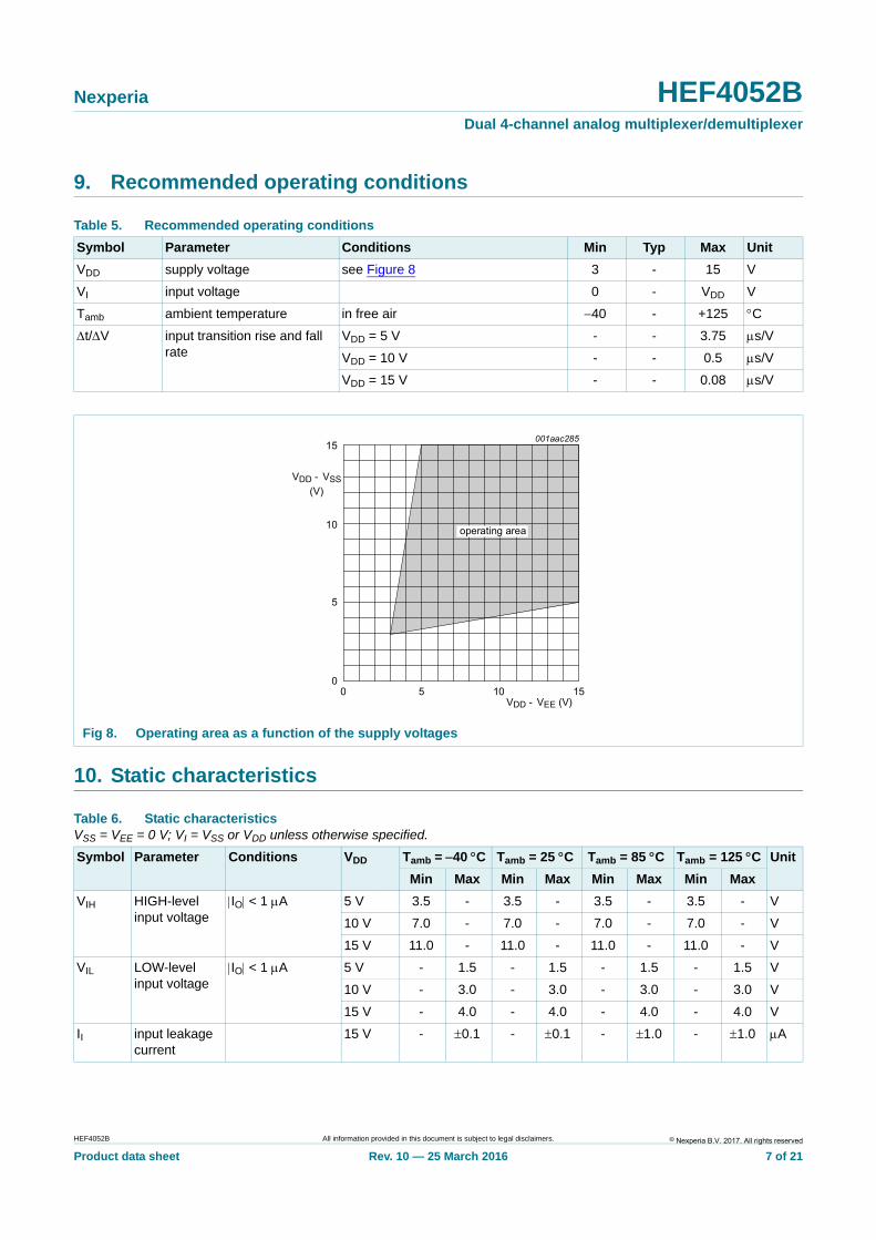
VDD supply voltage see Figure 8 3 - 15 V
VI input voltage 0 - VDD V
Tamb ambient temperature in free air 40 - +125 C
t/V input transition rise and fall rate
VDD = 5 V - - 3.75 s/V
VDD = 10 V - - 0.5 s/V
VDD = 15 V - - 0.08 s/V
Fig 8. Operating area as a function of the supply voltages
Table 6. Static characteristicsVSS = VEE = 0 V; VI = VSS or VDD unless otherwise specified.
Symbol Parameter Conditions VDD Tamb = 40 C Tamb = 25 C Tamb = 85 C Tamb = 125 C Unit
Min Max Min Max Min Max Min Max
VIH HIGH-level input voltage
IO < 1 A 5 V 3.5 - 3.5 - 3.5 - 3.5 - V
10 V 7.0 - 7.0 - 7.0 - 7.0 - V
15 V 11.0 - 11.0 - 11.0 - 11.0 - V
VIL LOW-level input voltage
IO < 1 A 5 V - 1.5 - 1.5 - 1.5 - 1.5 V
10 V - 3.0 - 3.0 - 3.0 - 3.0 V
15 V - 4.0 - 4.0 - 4.0 - 4.0 V
II input leakage current
15 V - 0.1 - 0.1 - 1.0 - 1.0 A
© Nexperia B.V. 2017. All rights reservedHEF4052B All information provided in this document is subject to legal disclaimers.
Product data sheet Rev. 10 — 25 March 2016 7 of 21
Nexperia HEF4052BDual 4-channel analog multiplexer/demultiplexer
10.1 Test circuits
IS(OFF) OFF-state leakage current
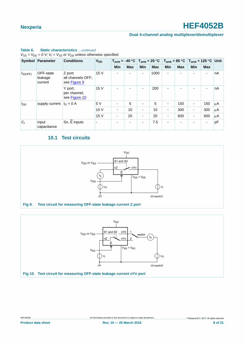
Z port; all channels OFF; see Figure 9
15 V - - - 1000 - - - - nA
Y port; per channel; see Figure 10
15 V - - - 200 - - - - nA
IDD supply current IO = 0 A 5 V - 5 - 5 - 150 - 150 A
10 V - 10 - 10 - 300 - 300 A
15 V - 20 - 20 - 600 - 600 A
CI input capacitance
Sn, E inputs - - - - 7.5 - - - - pF
Table 6. Static characteristics …continuedVSS = VEE = 0 V; VI = VSS or VDD unless otherwise specified.
Symbol Parameter Conditions VDD Tamb = 40 C Tamb = 25 C Tamb = 85 C Tamb = 125 C Unit
Min Max Min Max Min Max Min Max
Fig 9. Test circuit for measuring OFF-state leakage current Z port
Fig 10. Test circuit for measuring OFF-state leakage current nYn port
© Nexperia B.V. 2017. All rights reservedHEF4052B All information provided in this document is subject to legal disclaimers.
Product data sheet Rev. 10 — 25 March 2016 8 of 21
Nexperia HEF4052BDual 4-channel analog multiplexer/demultiplexer
10.2 On resistance
10.2.1 On resistance waveform and test circuit
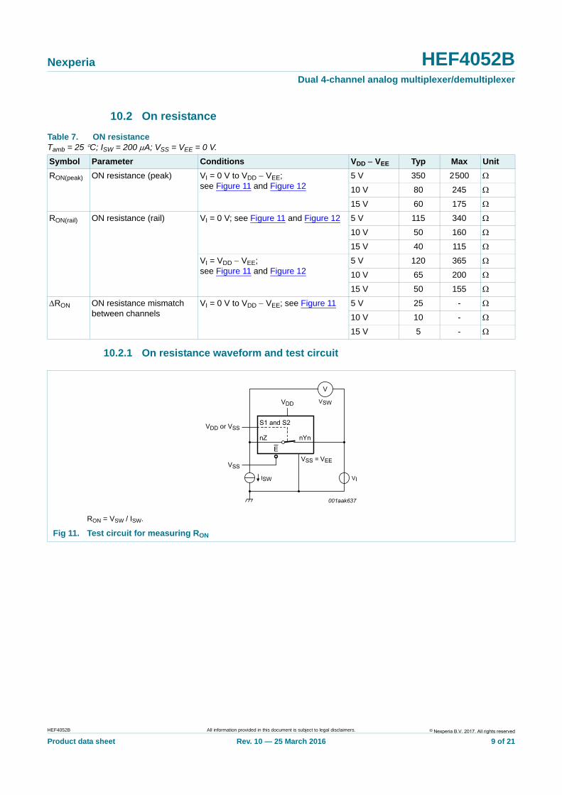
Table 7. ON resistanceTamb = 25 C; ISW = 200 A; VSS = VEE = 0 V.
Symbol Parameter Conditions VDD VEE Typ Max Unit
RON(peak) ON resistance (peak) VI = 0 V to VDD VEE; see Figure 11 and Figure 12
5 V 350 2500
10 V 80 245
15 V 60 175
RON(rail) ON resistance (rail) VI = 0 V; see Figure 11 and Figure 12 5 V 115 340
10 V 50 160
15 V 40 115
VI = VDD VEE; see Figure 11 and Figure 12
5 V 120 365
10 V 65 200
15 V 50 155
RON ON resistance mismatch between channels
VI = 0 V to VDD VEE; see Figure 11 5 V 25 -
10 V 10 -
15 V 5 -
RON = VSW / ISW.
Fig 11. Test circuit for measuring RON
© Nexperia B.V. 2017. All rights reservedHEF4052B All information provided in this document is subject to legal disclaimers.
Product data sheet Rev. 10 — 25 March 2016 9 of 21
Nexperia HEF4052BDual 4-channel analog multiplexer/demultiplexer
11. Dynamic characteristics
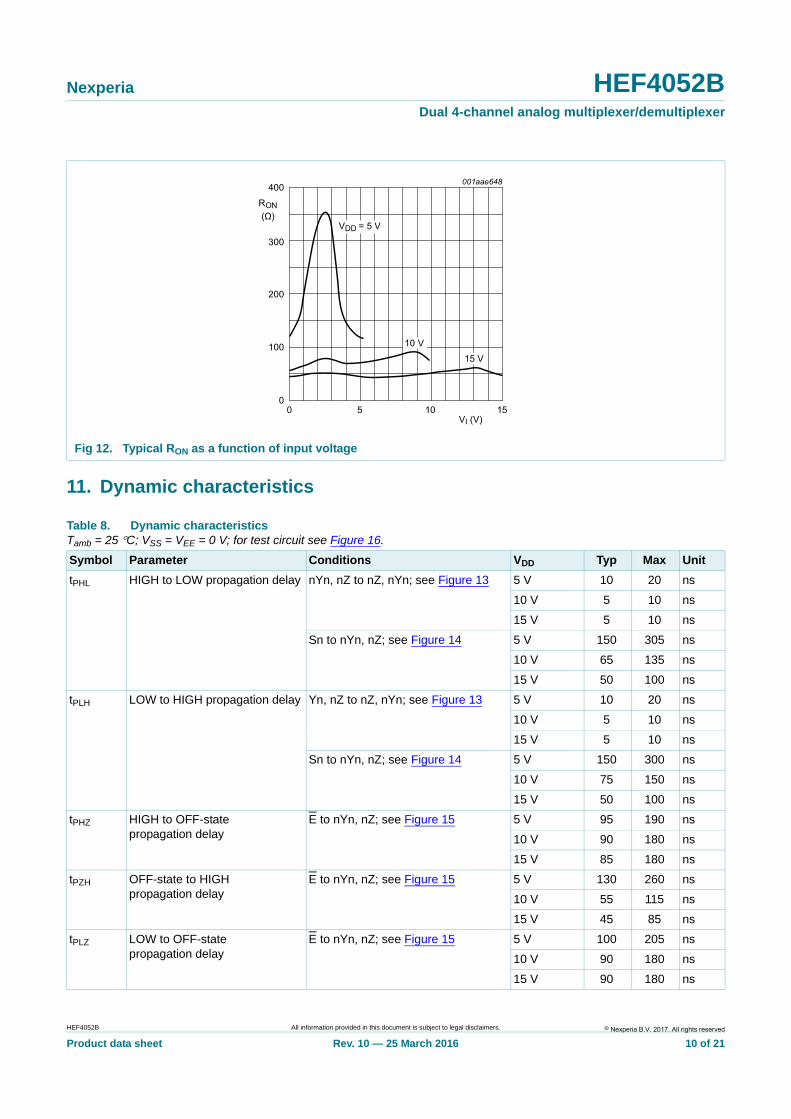
Fig 12. Typical RON as a function of input voltage
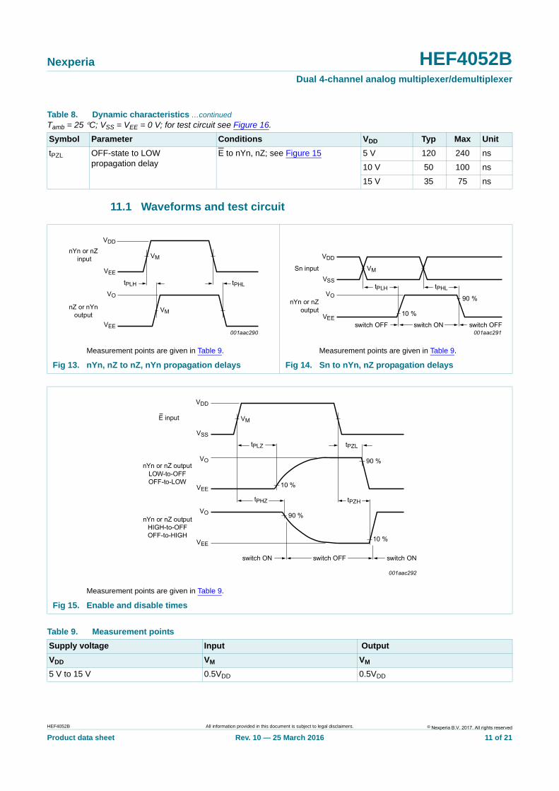
Table 8. Dynamic characteristicsTamb = 25 C; VSS = VEE = 0 V; for test circuit see Figure 16.
Symbol Parameter Conditions VDD Typ Max Unit
tPHL HIGH to LOW propagation delay nYn, nZ to nZ, nYn; see Figure 13 5 V 10 20 ns
10 V 5 10 ns
15 V 5 10 ns
Sn to nYn, nZ; see Figure 14 5 V 150 305 ns
10 V 65 135 ns
15 V 50 100 ns
tPLH LOW to HIGH propagation delay Yn, nZ to nZ, nYn; see Figure 13 5 V 10 20 ns
10 V 5 10 ns
15 V 5 10 ns
Sn to nYn, nZ; see Figure 14 5 V 150 300 ns
10 V 75 150 ns
15 V 50 100 ns
tPHZ HIGH to OFF-state propagation delay
E to nYn, nZ; see Figure 15 5 V 95 190 ns
10 V 90 180 ns
15 V 85 180 ns
tPZH OFF-state to HIGH propagation delay
E to nYn, nZ; see Figure 15 5 V 130 260 ns
10 V 55 115 ns
15 V 45 85 ns
tPLZ LOW to OFF-state propagation delay
E to nYn, nZ; see Figure 15 5 V 100 205 ns
10 V 90 180 ns
15 V 90 180 ns
© Nexperia B.V. 2017. All rights reservedHEF4052B All information provided in this document is subject to legal disclaimers.
Product data sheet Rev. 10 — 25 March 2016 10 of 21
Nexperia HEF4052BDual 4-channel analog multiplexer/demultiplexer
11.1 Waveforms and test circuit
tPZL OFF-state to LOW propagation delay
E to nYn, nZ; see Figure 15 5 V 120 240 ns
10 V 50 100 ns
15 V 35 75 ns
Table 8. Dynamic characteristics …continuedTamb = 25 C; VSS = VEE = 0 V; for test circuit see Figure 16.
Symbol Parameter Conditions VDD Typ Max Unit
Measurement points are given in Table 9. Measurement points are given in Table 9.
Fig 13. nYn, nZ to nZ, nYn propagation delays Fig 14. Sn to nYn, nZ propagation delays
Measurement points are given in Table 9.
Fig 15. Enable and disable times
Table 9. Measurement points
Supply voltage Input Output
VDD VM VM
5 V to 15 V 0.5VDD 0.5VDD
© Nexperia B.V. 2017. All rights reservedHEF4052B All information provided in this document is subject to legal disclaimers.
Product data sheet Rev. 10 — 25 March 2016 11 of 21
Nexperia HEF4052BDual 4-channel analog multiplexer/demultiplexer
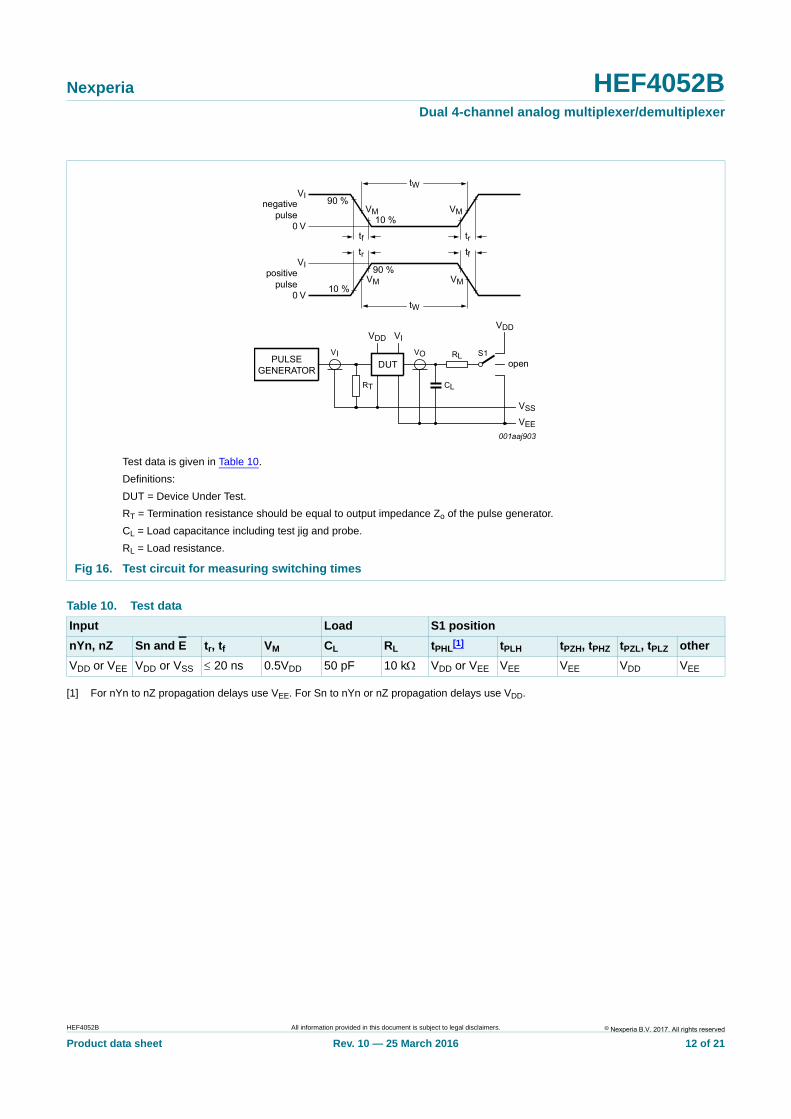
[1] For nYn to nZ propagation delays use VEE. For Sn to nYn or nZ propagation delays use VDD.
Test data is given in Table 10.
Definitions:
DUT = Device Under Test.
RT = Termination resistance should be equal to output impedance Zo of the pulse generator.
CL = Load capacitance including test jig and probe.
RL = Load resistance.
Fig 16. Test circuit for measuring switching times
Table 10. Test data
Input Load S1 position
nYn, nZ Sn and E tr, tf VM CL RL tPHL[1] tPLH tPZH, tPHZ tPZL, tPLZ other
VDD or VEE VDD or VSS 20 ns 0.5VDD 50 pF 10 k VDD or VEE VEE VEE VDD VEE
© Nexperia B.V. 2017. All rights reservedHEF4052B All information provided in this document is subject to legal disclaimers.
Product data sheet Rev. 10 — 25 March 2016 12 of 21
Nexperia HEF4052BDual 4-channel analog multiplexer/demultiplexer
11.2 Additional dynamic parameters
[1] fi is biased at 0.5 VDD; VI = 0.5VDD (p-p).
11.2.1 Test circuits
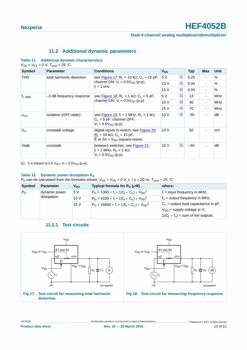
Table 11. Additional dynamic characteristicsVSS = VEE = 0 V; Tamb = 25 C.
Symbol Parameter Conditions VDD Typ Max Unit
THD total harmonic distortion see Figure 17; RL = 10 k; CL = 15 pF; channel ON; VI = 0.5VDD (p-p); fi = 1 kHz
5 V [1] 0.25 - %
10 V [1] 0.04 - %
15 V [1] 0.04 - %
f(3dB) 3 dB frequency response see Figure 18; RL = 1 k; CL = 5 pF; channel ON; VI = 0.5VDD (p-p)
5 V [1] 13 - MHz
10 V [1] 40 - MHz
15 V [1] 70 - MHz
iso isolation (OFF-state) see Figure 19; fi = 1 MHz; RL = 1 k; CL = 5 pF; channel OFF; VI = 0.5VDD (p-p)
10 V [1] 50 - dB
Vct crosstalk voltage digital inputs to switch; see Figure 20; RL = 10 k; CL = 15 pF; E or Sn = VDD (square-wave)
10 V 50 - mV
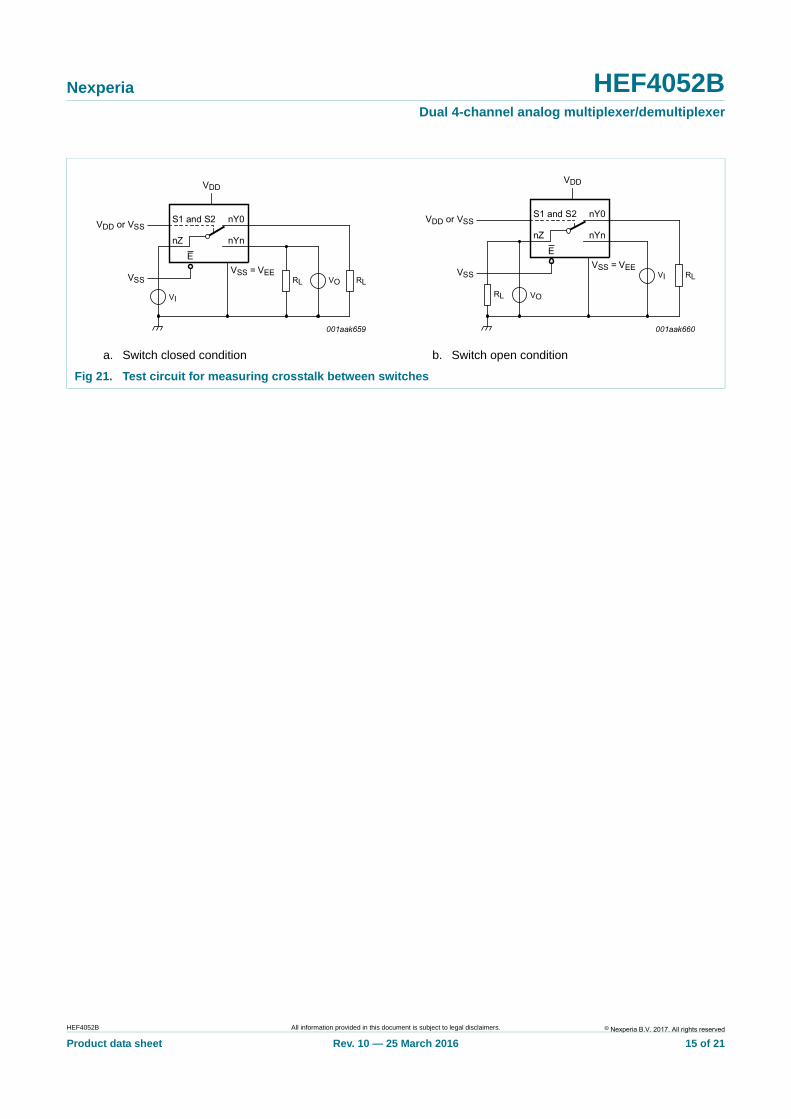
Xtalk crosstalk between switches; see Figure 21; fi = 1 MHz; RL = 1 k; VI = 0.5VDD (p-p)
10 V [1] 50 - dB
Table 12. Dynamic power dissipation PDPD can be calculated from the formulas shown; VEE = VSS = 0 V; tr = tf 20 ns; Tamb = 25 C.
Symbol Parameter VDD Typical formula for PD (W) where:
PD dynamic power dissipation
5 V PD = 1300 fi + (fo CL) VDD2 fi = input frequency in MHz;
fo = output frequency in MHz;
CL = output load capacitance in pF;
VDD = supply voltage in V;
(CL fo) = sum of the outputs.
10 V PD = 6100 fi + (fo CL) VDD2
15 V PD = 15600 fi + (fo CL) VDD2
Fig 17. Test circuit for measuring total harmonic distortion
Fig 18. Test circuit for measuring frequency response
© Nexperia B.V. 2017. All rights reservedHEF4052B All information provided in this document is subject to legal disclaimers.
Product data sheet Rev. 10 — 25 March 2016 13 of 21
Nexperia HEF4052BDual 4-channel analog multiplexer/demultiplexer
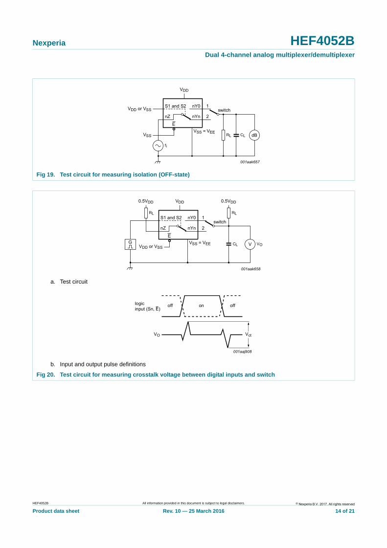
Fig 19. Test circuit for measuring isolation (OFF-state)
a. Test circuit
b. Input and output pulse definitions
Fig 20. Test circuit for measuring crosstalk voltage between digital inputs and switch
© Nexperia B.V. 2017. All rights reservedHEF4052B All information provided in this document is subject to legal disclaimers.
Product data sheet Rev. 10 — 25 March 2016 14 of 21
Nexperia HEF4052BDual 4-channel analog multiplexer/demultiplexer
a. Switch closed condition b. Switch open condition
Fig 21. Test circuit for measuring crosstalk between switches
© Nexperia B.V. 2017. All rights reservedHEF4052B All information provided in this document is subject to legal disclaimers.
Product data sheet Rev. 10 — 25 March 2016 15 of 21
Nexperia HEF4052BDual 4-channel analog multiplexer/demultiplexer
12. Package outline
Fig 22. Package outline SOT109-1 (SO16)
© Nexperia B.V. 2017. All rights reservedHEF4052B All information provided in this document is subject to legal disclaimers.
Product data sheet Rev. 10 — 25 March 2016 16 of 21
Nexperia HEF4052BDual 4-channel analog multiplexer/demultiplexer
Fig 23. Package outline SOT403-1 (TSSOP16)
© Nexperia B.V. 2017. All rights reservedHEF4052B All information provided in this document is subject to legal disclaimers.
Product data sheet Rev. 10 — 25 March 2016 17 of 21
Nexperia HEF4052BDual 4-channel analog multiplexer/demultiplexer
13. Abbreviations
14. Revision history
Table 13. Abbreviations
Acronym Description
DUT Device Under Test
Table 14. Revision history
Document ID Release date Data sheet status Change notice Supersedes
HEF4052B v.10 20160325 Product data sheet - HEF4052B v.9
Modifications: • Type number HEF4052BP (SOT38-4) removed.
HEF4052B v.9 20140911 Product data sheet - HEF4052B v.8
Modifications: • Figure 20: Test circuit modified
HEF4052B v.8 20111117 Product data sheet - HEF4052B v.7
Modifications: • Legal pages updated.
• Changes in “General description”, “Features and benefits” and “Applications”.
HEF4052B v.7 20100326 Product data sheet - HEF4052B v.6
HEF4052B v.6 20100308 Product data sheet - HEF4052B v.5
HEF4052B v.5 20091127 Product data sheet - HEF4052B v.4
HEF4052B v.4 20090924 Product data sheet - HEF4052B_CNV v.3
HEF4052B_CNV v.3 19950101 Product specification - HEF4052B_CNV v.2
HEF4052B_CNV v.2 19950101 Product specification - -
© Nexperia B.V. 2017. All rights reservedHEF4052B All information provided in this document is subject to legal disclaimers.
Product data sheet Rev. 10 — 25 March 2016 18 of 21
Nexperia HEF4052BDual 4-channel analog multiplexer/demultiplexer
15. Legal information
15.1 Data sheet status
[1] Please consult the most recently issued document before initiating or completing a design.
[2] The term ‘short data sheet’ is explained in section “Definitions”.
[3] The product status of device(s) described in this document may have changed since this document was published and may differ in case of multiple devices. The latest product status information is available on the Internet at URL http://www.nexperia.com.
15.2 Definitions
Draft — The document is a draft version only. The content is still under internal review and subject to formal approval, which may result in modifications or additions. Nexperia does not give any representations or warranties as to the accuracy or completeness of information included herein and shall have no liability for the consequences of use of such information.
Short data sheet — A short data sheet is an extract from a full data sheet with the same product type number(s) and title. A short data sheet is intended for quick reference only and should not be relied upon to contain detailed and full information. For detailed and full information see the relevant full data sheet, which is available on request via the local Nexperia sales office. In case of any inconsistency or conflict with the short data sheet, the full data sheet shall prevail.
Product specification — The information and data provided in a Product data sheet shall define the specification of the product as agreed between Nexperia and its customer, unless Nexperia and customer have explicitly agreed otherwise in writing. In no event however, shall an agreement be valid in which the Nexperia product is deemed to offer functions and qualities beyond those described in the Product data sheet.
15.3 Disclaimers
Limited warranty and liability — Information in this document is believed to be accurate and reliable. However, Nexperia does not give any representations or warranties, expressed or implied, as to the accuracy or completeness of such information and shall have no liability for the consequences of use of such information. Nexperia takes no responsibility for the content in this document if provided by an information source outside of Nexperia.
In no event shall Nexperia be liable for any indirect, incidental, punitive, special or consequential damages (including - without limitation - lost profits, lost savings, business interruption, costs related to the removal or replacement of any products or rework charges) whether or not such damages are based on tort (including negligence), warranty, breach of contract or any other legal theory.
Notwithstanding any damages that customer might incur for any reason whatsoever, Nexperia’s aggregate and cumulative liability towards customer for the products described herein shall be limited in accordance with the Terms and conditions of commercial sale of Nexperia.
Right to make changes — Nexperia reserves the right to make changes to information published in this document, including without limitation specifications and product descriptions, at any time and without notice. This document supersedes and replaces all information supplied prior to the publication hereof.
Suitability for use — Nexperia products are not designed, authorized or warranted to be suitable for use in life support, life-critical or safety-critical systems or equipment, nor in applications where failure or malfunction of a Nexperia product can reasonably be expected to result in personal injury, death or severe property or environmental damage. Nexperia and its suppliers accept no liability for inclusion and/or use of Nexperia products in such equipment or applications and therefore such inclusion and/or use is at the customer’s own risk.
Applications — Applications that are described herein for any of these products are for illustrative purposes only. Nexperia makes no representation or warranty that such applications will be suitable for the specified use without further testing or modification.
Customers are responsible for the design and operation of their applications and products using Nexperia products, and Nexperia accepts no liability for any assistance with applications or customer product design. It is customer’s sole responsibility to determine whether the Nexperia product is suitable and fit for the customer’s applications and products planned, as well as for the planned application and use of customer’s third party customer(s). Customers should provide appropriate design and operating safeguards to minimize the risks associated with their applications and products.
Nexperia does not accept any liability related to any default, damage, costs or problem which is based on any weakness or default in the customer’s applications or products, or the application or use by customer’s third party customer(s). Customer is responsible for doing all necessary testing for the customer’s applications and products using Nexperia products in order to avoid a default of the applications and the products or of the application or use by customer’s third party customer(s). Nexperia does not accept any liability in this respect.
Limiting values — Stress above one or more limiting values (as defined in the Absolute Maximum Ratings System of IEC 60134) will cause permanent damage to the device. Limiting values are stress ratings only and (proper) operation of the device at these or any other conditions above those given in the Recommended operating conditions section (if present) or the Characteristics sections of this document is not warranted. Constant or repeated exposure to limiting values will permanently and irreversibly affect the quality and reliability of the device.
Terms and conditions of commercial sale — Nexperia products are sold subject to the general terms and conditions of commercial sale, as published at http://www.nexperia.com/profile/terms, unless otherwise agreed in a valid written individual agreement. In case an individual agreement is concluded only the terms and conditions of the respective agreement shall apply. Nexperia hereby expressly objects to applying the customer’s general terms and conditions with regard to the purchase of Nexperia products by customer.
No offer to sell or license — Nothing in this document may be interpreted or construed as an offer to sell products that is open for acceptance or the grant, conveyance or implication of any license under any copyrights, patents or other industrial or intellectual property rights.
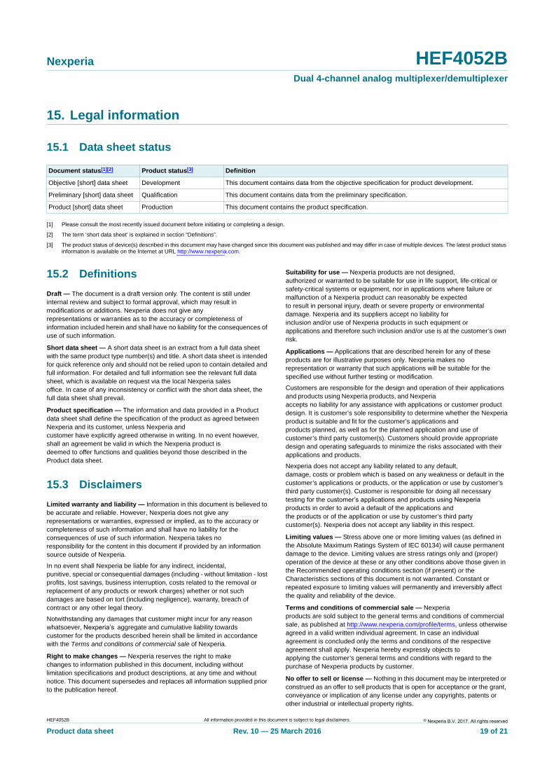
Document status[1][2] Product status[3] Definition
Objective [short] data sheet Development This document contains data from the objective specification for product development.
Preliminary [short] data sheet Qualification This document contains data from the preliminary specification.
Product [short] data sheet Production This document contains the product specification.
© Nexperia B.V. 2017. All rights reservedHEF4052B All information provided in this document is subject to legal disclaimers.
Product data sheet Rev. 10 — 25 March 2016 19 of 21
Nexperia HEF4052BDual 4-channel analog multiplexer/demultiplexer
Export control — This document as well as the item(s) described herein may be subject to export control regulations. Export might require a prior authorization from competent authorities.
Non-automotive qualified products — Unless this data sheet expressly states that this specific Nexperia product is automotive qualified, the product is not suitable for automotive use. It is neither qualified nor tested in accordance with automotive testing or application requirements. Nexperia accepts no liability for inclusion and/or use of non-automotive qualified products in automotive equipment or applications.
In the event that customer uses the product for design-in and use in automotive applications to automotive specifications and standards, customer (a) shall use the product without Nexperia’s warranty of the product for such automotive applications, use and specifications, and (b) whenever customer uses the product for automotive applications beyond
Nexperia’s specifications such use shall be solely at customer’s own risk, and (c) customer fully indemnifies Nexperia for any liability, damages or failed product claims resulting from customer design and use of the product for automotive applications beyond Nexperia’s standard warranty and Nexperia’s product specifications.
Translations — A non-English (translated) version of a document is for reference only. The English version shall prevail in case of any discrepancy between the translated and English versions.
15.4 TrademarksNotice: All referenced brands, product names, service names and trademarks are the property of their respective owners.
16. Contact information
For more information, please visit: http://www.nexperia.com
For sales office addresses, please send an email to: [email protected]
© Nexperia B.V. 2017. All rights reservedHEF4052B All information provided in this document is subject to legal disclaimers.
Product data sheet Rev. 10 — 25 March 2016 20 of 21
Nexperia HEF4052BDual 4-channel analog multiplexer/demultiplexer
17. Contents
1 General description . . . . . . . . . . . . . . . . . . . . . . 1
2 Features and benefits . . . . . . . . . . . . . . . . . . . . 1
3 Applications . . . . . . . . . . . . . . . . . . . . . . . . . . . . 1
4 Ordering information. . . . . . . . . . . . . . . . . . . . . 2
5 Functional diagram . . . . . . . . . . . . . . . . . . . . . . 2
6 Pinning information. . . . . . . . . . . . . . . . . . . . . . 56.1 Pinning . . . . . . . . . . . . . . . . . . . . . . . . . . . . . . . 56.2 Pin description . . . . . . . . . . . . . . . . . . . . . . . . . 5
7 Functional description . . . . . . . . . . . . . . . . . . . 67.1 Function table . . . . . . . . . . . . . . . . . . . . . . . . . . 6
8 Limiting values. . . . . . . . . . . . . . . . . . . . . . . . . . 6
9 Recommended operating conditions. . . . . . . . 7
10 Static characteristics. . . . . . . . . . . . . . . . . . . . . 710.1 Test circuits . . . . . . . . . . . . . . . . . . . . . . . . . . . . 810.2 On resistance . . . . . . . . . . . . . . . . . . . . . . . . . . 910.2.1 On resistance waveform and test circuit. . . . . . 9
11 Dynamic characteristics . . . . . . . . . . . . . . . . . 1011.1 Waveforms and test circuit . . . . . . . . . . . . . . . 1111.2 Additional dynamic parameters . . . . . . . . . . . 1311.2.1 Test circuits . . . . . . . . . . . . . . . . . . . . . . . . . . . 13
12 Package outline . . . . . . . . . . . . . . . . . . . . . . . . 16
13 Abbreviations. . . . . . . . . . . . . . . . . . . . . . . . . . 18
14 Revision history. . . . . . . . . . . . . . . . . . . . . . . . 18
15 Legal information. . . . . . . . . . . . . . . . . . . . . . . 1915.1 Data sheet status . . . . . . . . . . . . . . . . . . . . . . 1915.2 Definitions. . . . . . . . . . . . . . . . . . . . . . . . . . . . 1915.3 Disclaimers . . . . . . . . . . . . . . . . . . . . . . . . . . . 1915.4 Trademarks. . . . . . . . . . . . . . . . . . . . . . . . . . . 20
16 Contact information. . . . . . . . . . . . . . . . . . . . . 20
17 Contents . . . . . . . . . . . . . . . . . . . . . . . . . . . . . . 21
© Nexperia B.V. 2017. All rights reservedFor more information, please visit: http://www.nexperia.comFor sales office addresses, please send an email to: [email protected] Date of release: 25 March 2016