Embed Size (px)
Citation preview
Choosing the Correct Switch, Multiplexer, or Protection Product for Your Application
www.analog.com/switch-mux
Analog Devices offers a large range of switches and multiplexers, covering single to multiple switch elements with various signal ranges, in a variety of packages to best suit customer application needs. Deciding on the best switch or multiplexer for your application can, therefore, be a difficult task.
The simplest switch (single-pole, single-throw—SPST) will connect or disconnect an analog signal when a digital input signal is applied. Increasing the number of throws will then allow the switching of one of many inputs to one single output. Some switches offer different transient behaviors when you move from one switch position to the other. In make-before-break switching, the moving contact never sees an open circuit. In break-before-make switching, the old contact is broken before the new one is made. This means that both contacts are never shorted to each other.
In the selection of the correct switch for your application, these are key specifications to consider:
• Supply voltage
• Performance
• New: Additional protection requirements
• Configuration
• Package
Supply VoltageDepending on the supply voltage that you require, Analog Devices can offer you a number of high performance switches and multiplexers to suit your application. Low voltage switches can offer performance advantages over higher voltage switches. High voltage switches are optimized when using the maximum signal range but are specified for use at lower voltages also.
Analog Devices offers a varied range of supply voltages:
• ±20 V • ±15 V
• ±5 V
• Low voltage (up to 5 V)
• Single- and dual-supply options
If, for example, you are using a 5 V power supply in your circuit and require a switch, then the best switch to choose would be one of our low voltage (0 V to 5 V rated) switches and not, for example, one of our high voltage (±15 V) parts. Likewise, if you require high voltage opera-tion, then the ±15 V will be optimized for operation at these voltages, and the performance will degrade as the voltage is reduced.
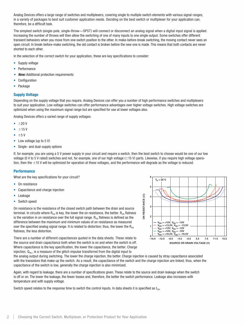
PerformanceWhat are the key specifications for your circuit?
• On resistance
• Capacitance and charge injection
• Leakage
• Switch speed
On resistance is the resistance of the closed switch path between the drain and source terminal. In circuits where RON is key, the lower the on resistance, the better. RON flatness is the variation in on resistance over the full signal range. RON flatness is defined as the difference between the maximum and minimum values of on resistance as measured over the specified analog signal range. It is related to distortion; thus, the lower the RON flatness, the less distortion.
There are a number of different capacitances quoted in the data sheets. These relate to the source and drain capacitance both when the switch is on and when the switch is off. Where capacitance is the key specification, the lower the capacitance, the better. Charge injection, QINJ, is a measure of the glitch impulse transferred from the digital input to the analog output during switching. The lower the charge injection, the better. Charge injection is caused by stray capacitance associated with the transistors that make up the switch. As a result, the capacitance of the switch and the charge injection are linked; thus, when the capacitance of the switch is low, generally the charge injection is also minimized.
Again, with regard to leakage, there are a number of specifications given. These relate to the source and drain leakage when the switch is off or on. The lower the leakage, the fewer losses and, therefore, the better the switch performance. Leakage also increases with temperature and with supply voltage.
Switch speed relates to the response time to switch the control inputs. In data sheets it is specified as tON.
5
6
0–16.5 15.5
SOURCE OR DRAIN VOLTAGE (V)
ON
RE
SIS
TA
NC
E (
)
4
3
2
1
–12.5 –8.5 –4.5 –0.5 3.5 7.5 11.5
VDD = +15V, VSS = –15VVDD = +13.5V, VSS = –13.5VVDD = +12V, VSS = –12VVDD = +10V, VSS = –10VVDD = +16.5V, VSS = –16.5V
TA = 25°C
2 | Choosing the Correct Switch, Multiplexer, or Protection Product for Your Application
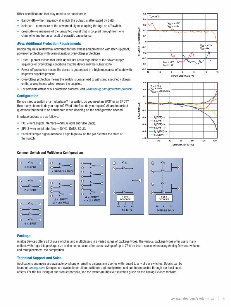
Other specifications that may need to be considered:
• Bandwidth—the frequency at which the output is attenuated by 3 dB.
• Isolation—a measure of the unwanted signal coupling through an off switch.
• Crosstalk—a measure of the unwanted signal that is coupled through from one channel to another as a result of parasitic capacitance.
New: Additional Protection RequirementsDo you require a switch/mux optimized for robustness and protection with latch-up proof, power-off protection (with overvoltage), or overvoltage protection?
• Latch-up proof means that latch-up will not occur regardless of the power supply sequence or overvoltage conditions that the device may be subjected to.
• Power-off protection means the device is guaranteed in a high impedance off state with no power supplies present.
• Overvoltage protection means the switch is guaranteed to withstand specified voltages on the analog inputs which exceed the supplies.
• For complete details of our protection products, visit www.analog.com/protection-products.
ConfigurationDo you need a switch or a multiplexer? If a switch, do you need an SPST or an SPDT? How many channels do you require? What interface do you require? All are important questions that need to be considered when deciding on the configuration needed.
Interface options are as follows:
• I2C: 2-wire digital interface—SCL (clock) and SDA (data).
• SPI: 3-wire serial interface—SYNC, DATA, SCLK.
• Parallel: simple digital interface. Logic high/low on the pin dictates the state of the switch.
Common Switch and Multiplexer Configurations
PackageAnalog Devices offers all of our switches and multiplexers in a varied range of package types. The various package types offer users many options with regard to package size and in some cases offer users savings of up to 75% on board space when using Analog Devices switches and multiplexers vs. the competition.
Technical Support and SalesApplications engineers are available by phone or email to discuss any queries with regard to any of our switches. Details can be found on analog.com. Samples are available for all our switches and multiplexers and can be requested through our local sales offices. For the full listing of our product portfolio, see the switch/multiplexer selection guide on the Analog Devices website.
0.5
–0.5–15 15
INPUT VOLTAGE (V)
CH
AR
GE
IN
JEC
TIO
N (
pC
)
0.4
0.3
0.2
0.1
0
–0.1
–0.2
–0.3
–0.4
–10 –5 0 5 10
TA = 25°C
VDD = +15VVSS = –15V
VDD = +5VVSS = –5V
VDD = +12VVSS = 0V
0.6
–1.00
TEMPERATURE (°C)
LE
AK
AG
E (
nA
)20 40 60 80 100 120
IS(OFF)+–
ID(OFF)+–
IS(OFF)–+
ID(OFF)–+
ID, IS(ON)++
ID, IS(ON)– –
0.4
0.2
0
–0.2
–0.4
–0.6
–0.8
VDD = 15VVSS = –15VVBIAS = +10V/–10V
1 × SPDT/2:1 MUX
2 × SPDT/2 × 2:1 MUX
4 × SPDT/4 × 2:1 MUX
1 × SPST
2 × SPST
4 × SPST
8:1 MUX
1 OF 8DECODER
A0 A2A1
1
2
8
1A
A
B
4A
1B
4B
DIFF 4:1 MUX
1 OF 4DECODER
A0 ENA1
www.analog.com/switch-mux | 3
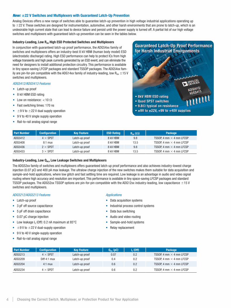
New: ∙22 V Switches and Multiplexers with Guaranteed Latch-Up PreventionAnalog Devices offers a new range of switches able to guarantee latch-up prevention in high voltage industrial applications operating up to ±22 V. These switches are designed for instrumentation, automotive, and other harsh environments that are prone to latch-up, which is an undesirable high current state that can lead to device failure and persist until the power supply is turned off. A partial list of our high voltage switches and multiplexers with guaranteed latch-up prevention can be seen in the tables below.
Industry-Leading, Low Ron High ESd Protected Switches and Multiplexers
In conjunction with guaranteed latch-up proof performance, the ADG54xx family of switches and multiplexers offers an industry-best 8 kV HBM (human body model) ESD (electrostatic discharge) rating. High ESD performance can help to protect ICs from high voltage transients and high peak currents generated by an ESD event, and can eliminate the need for designers to install additional protection circuitry. This performance is available in tiny space-saving LFCSP packages and standard TSSOP packages. The ADG54xx fam-ily are pin-for-pin compatible with the ADG14xx family of industry-leading, low RON ±15 V switches and multiplexers.
Part number Configuration Key Feature ESd Rating Ron (𝛀) Package
ADG5412 4 × SPST Latch-up proof 8 kV HBM 9.8 TSSOP, 4 mm × 4 mm LFCSP
ADG5408 8:1 mux Latch-up proof 8 kV HBM 13.5 TSSOP, 4 mm × 4 mm LFCSP
ADG5436 2 × SPDT Latch-up proof 8 kV HBM 9.8 TSSOP, 4 mm × 4 mm LFCSP
ADG5433 3 × SPDT Latch-up proof 8 kV HBM 13.5 TSSOP, 4 mm × 4 mm LFCSP
Industry-Leading, Low QInj, Low Leakage Switches and Multiplexers
The ADG52xx family of switches and multiplexers offers guaranteed latch-up proof performance and also achieves industry-lowest charge injection (0.07 pC) and 400 pA max leakage. The ultralow charge injection of the new switches makes them suitable for data acquisition and sample-and-hold applications, where low glitch and fast settling time are required. Low leakage is an advantage in audio and video signal routing where high accuracy and resolution are important. This performance is available in tiny space-saving LFCSP packages and standard TSSOP packages. The ADG52xx TSSOP options are pin-for-pin compatible with the ADG12xx industry-leading, low capacitance ±15 V switches and multiplexers.
ADG5212/ADG5213 Features
• Latch-up proof
• 3 pF off source capacitance
• 5 pF off drain capacitance
• 0.07 pC charge injection
• Low leakage IS (Off): 0.2 nA maximum at 85°C
• ±9 V to ±22 V dual-supply operation
• 9 V to 40 V single-supply operation
• Rail-to-rail analog signal range
Applications
• Data acquisition systems
• Industrial process control systems
• Data bus switching
• Audio and video routing
• Sample-and-hold systems
• Relay replacement
Part number Configuration Key Feature QInj (pC) IS (off) PackageADG5213 4 × SPST Latch-up proof 0.07 0.2 TSSOP, 4 mm × 4 mm LFCSP
ADG5209 Diff 4:1 mux Latch-up proof 0.4 0.2 TSSOP, 4 mm × 4 mm LFCSP
ADG5204 4:1 mux Latch-up proof 0.6 0.2 TSSOP, 4 mm × 4 mm LFCSP
ADG5234 4 × SPDT Latch-up proof 0.6 0.2 TSSOP, 4 mm × 4 mm LFCSP
ADG5412/ADG5413 Features
• Latch-up proof
• 8 kV HBM ESD rating
• Low on resistance: < 10 Ω• Fast switching times: 170 ns
• ±9 V to ±22 V dual supply operation
• 9 V to 40 V single supply operation
• Rail-to-rail analog signal range
4 | Choosing the Correct Switch, Multiplexer, or Protection Product for Your Application
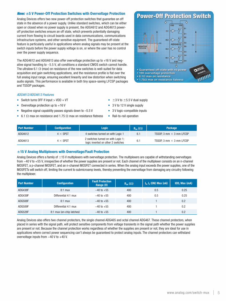
New: ∙5 V Power-off Protection Switches with overvoltage Protection Analog Devices offers two new power-off protection switches that guarantee an off state in the absence of a power supply. Unlike standard switches, which can be either open or closed when no power supply is present, the ADG4612 and ADG4613 power-off protection switches ensure an off state, which prevents potentially damaging current from flowing to circuit boards used in data communications, communications infrastructure systems, and other sensitive equipment. The guaranteed off-state feature is particularly useful in applications where analog signals may be present at the switch inputs before the power supply voltage is on, or where the user has no control over the power supply sequence.
The ADG4612 and ADG4613 also offer overvoltage protection up to +16 V and neg-ative signal handling to –5.5 V, all conditions a standard CMOS switch cannot handle. The ultralow 6.1 Ω (max) on resistance of the new switches is well-suited for data acquisition and gain switching applications, and the resistance profile is flat over the full analog input range, ensuring excellent linearity and low distortion when switching audio signals. This performance is available in both tiny space-saving LFCSP packages and TSSOP packages.
ADG4612/ADG4613 Features
• Switch turns OFF if input > VDD + VT
• Overvoltage protection up to +16 V
• Negative signal capability passes signals down to –5.5 V
• 6.1 Ω max on resistance and 1.75 Ω max on resistance flatness
• ±3 V to ±5.5 V dual supply
• 3 V to 12 V single supply
• 3 V logic-compatible inputs
• Rail-to-rail operation
Part number Configuration Logic Ron (𝛀) Package
ADG4612 4 × SPST 4 switches turned on with Logic 1 6.1 TSSOP, 3 mm × 3 mm LFCSP
ADG4613 4 × SPST2 switches turned on with Logic 1; logic inverted on other 2 switches
6.1 TSSOP, 3 mm × 3 mm LFCSP
∙15 V Analog Multiplexers with overvoltage/Fault ProtectionAnalog Devices offers a family of ±15 V multiplexers with overvoltage protection. The multiplexers are capable of withstanding overvoltages from −40 V to +55 V, irrespective of whether the power supplies are present or not. Each channel of the multiplexer consists on an n-channel MOSFET, a p-channel MOSFET, and an n-channel MOSFET connected in series. When the analog input exceeds the power supplies, one of the MOSFETs will switch off, limiting the current to submicroamp levels, thereby preventing the overvoltage from damaging any circuitry following the multiplexer.
Part number ConfigurationFault Protection
Range (V) Ron (𝛀) Id, IS (on) Max (nA) Idd, Max (mA)
ADG438F 8:1 mux −40 to +55 400 0.5 0.25
ADG439F Differential 4:1 mux −40 to +55 400 0.5 0.25
ADG508F 8:1 mux −40 to +55 400 1 0.2
ADG509F Differential 4:1 mux −40 to +55 400 1 0.2
ADG528F 8:1 mux (on-chip latches) −40 to +55 400 1 0.2
Analog Devices also offers two channel protectors, the single channel ADG465 and octal channel ADG467. These channel protectors, when placed in series with the signal path, will protect sensitive components from voltage transients in the signal path whether the power supplies are present or not. Because the channel protection works regardless of whether the supplies are present or not, they are ideal for use in applications where correct power sequencing can’t always be guaranteed to protect analog inputs. The channel protectors can withstand overvoltage inputs from −40 V to +40 V.
www.analog.com/switch-mux | 5
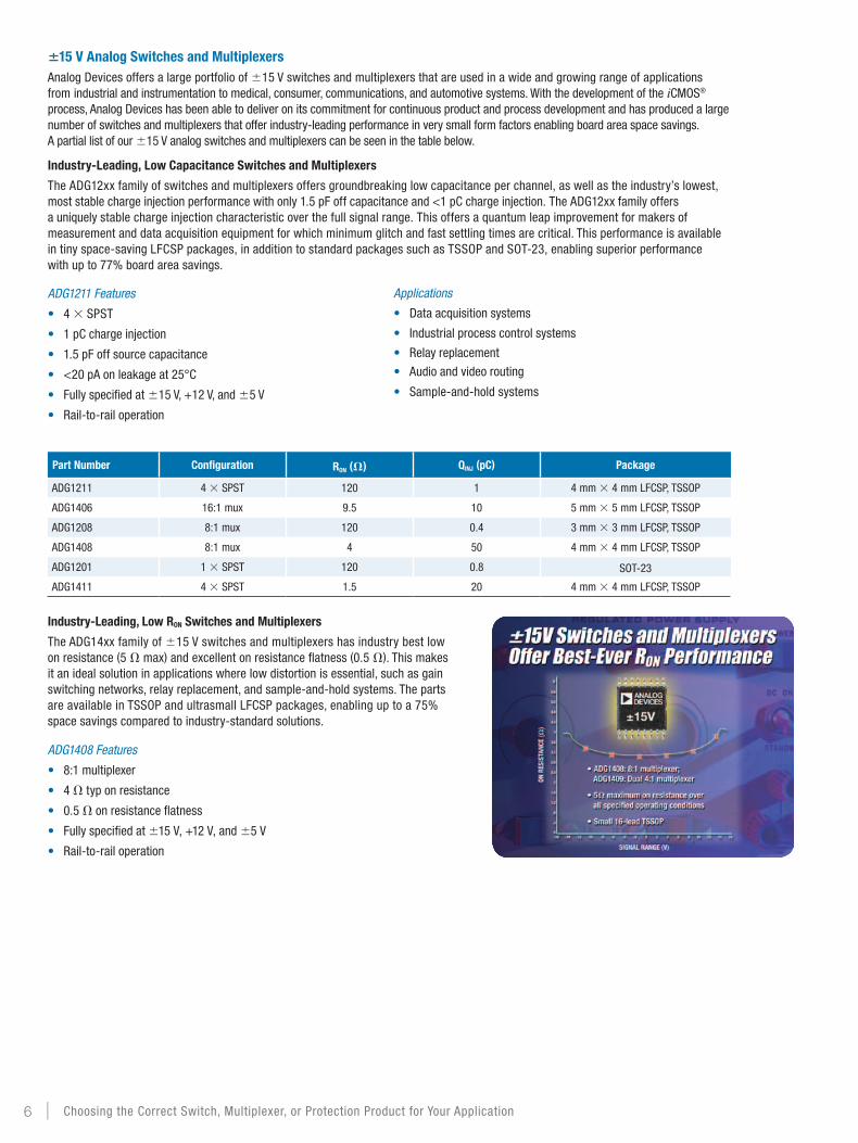
∙15 V Analog Switches and MultiplexersAnalog Devices offers a large portfolio of ±15 V switches and multiplexers that are used in a wide and growing range of applications from industrial and instrumentation to medical, consumer, communications, and automotive systems. With the development of the iCMOS® process, Analog Devices has been able to deliver on its commitment for continuous product and process development and has produced a large number of switches and multiplexers that offer industry-leading performance in very small form factors enabling board area space savings. A partial list of our ±15 V analog switches and multiplexers can be seen in the table below.
Industry-Leading, Low Capacitance Switches and Multiplexers
The ADG12xx family of switches and multiplexers offers groundbreaking low capacitance per channel, as well as the industry’s lowest, most stable charge injection performance with only 1.5 pF off capacitance and <1 pC charge injection. The ADG12xx family offers a uniquely stable charge injection characteristic over the full signal range. This offers a quantum leap improvement for makers of measurement and data acquisition equipment for which minimum glitch and fast settling times are critical. This performance is available in tiny space-saving LFCSP packages, in addition to standard packages such as TSSOP and SOT-23, enabling superior performance with up to 77% board area savings.
ADG1211 Features
• 4 × SPST
• 1 pC charge injection
• 1.5 pF off source capacitance
• <20 pA on leakage at 25°C
• Fully specified at ±15 V, +12 V, and ±5 V
• Rail-to-rail operation
Applications
• Data acquisition systems
• Industrial process control systems
• Relay replacement
• Audio and video routing
• Sample-and-hold systems
Part number Configuration Ron (𝛀) QInj (pC) Package
ADG1211 4 × SPST 120 1 4 mm × 4 mm LFCSP, TSSOP
ADG1406 16:1 mux 9.5 10 5 mm × 5 mm LFCSP, TSSOP
ADG1208 8:1 mux 120 0.4 3 mm × 3 mm LFCSP, TSSOP
ADG1408 8:1 mux 4 50 4 mm × 4 mm LFCSP, TSSOP
ADG1201 1 × SPST 120 0.8 SOT-23
ADG1411 4 × SPST 1.5 20 4 mm × 4 mm LFCSP, TSSOP
Industry-Leading, Low Ron Switches and Multiplexers
The ADG14xx family of ±15 V switches and multiplexers has industry best low on resistance (5 Ω max) and excellent on resistance flatness (0.5 Ω). This makes it an ideal solution in applications where low distortion is essential, such as gain switching networks, relay replacement, and sample-and-hold systems. The parts are available in TSSOP and ultrasmall LFCSP packages, enabling up to a 75% space savings compared to industry-standard solutions.
ADG1408 Features
• 8:1 multiplexer
• 4 Ω typ on resistance
• 0.5 Ω on resistance flatness
• Fully specified at ±15 V, +12 V, and ±5 V
• Rail-to-rail operation
6 | Choosing the Correct Switch, Multiplexer, or Protection Product for Your Application
∙5 V Analog Switches and MultiplexersAnalog Devices offers a portfolio of ±5 V switches and multiplexers that are used in a wide and growing range of applications from industrial and instrumentation to medi-cal, consumer, communications, and automotive systems. There are products optimized for low on resistance and products for low capacitance and charge injection. A partial list of our ±5 V analog switches and multiplexers can be seen in the table below.
Part number Configuration Ron (𝛀) QInj (pC) Package
ADG601/ADG602 1 × SPST 2 250 MSOP, SOT-23
ADG604 4:1 mux 85 1 TSSOP
ADG608/ADG609 8:1 diff, 4:1 mux 22 6 TSSOP, SOIC
ADG611/ADG612/ADG613 4 × SPST 85 0.5 TSSOP
ADG619/ADG620 1 × SPDT 4 110 MSOP, SOT-23
ADG1604 4:1 mux 1 140 TSSOP, 4 mm × 4 mm LFCSP
ADG1611/ADG1612/ADG1613
4 × SPST 1 140 TSSOP, 4 mm × 4 mm LFCSP
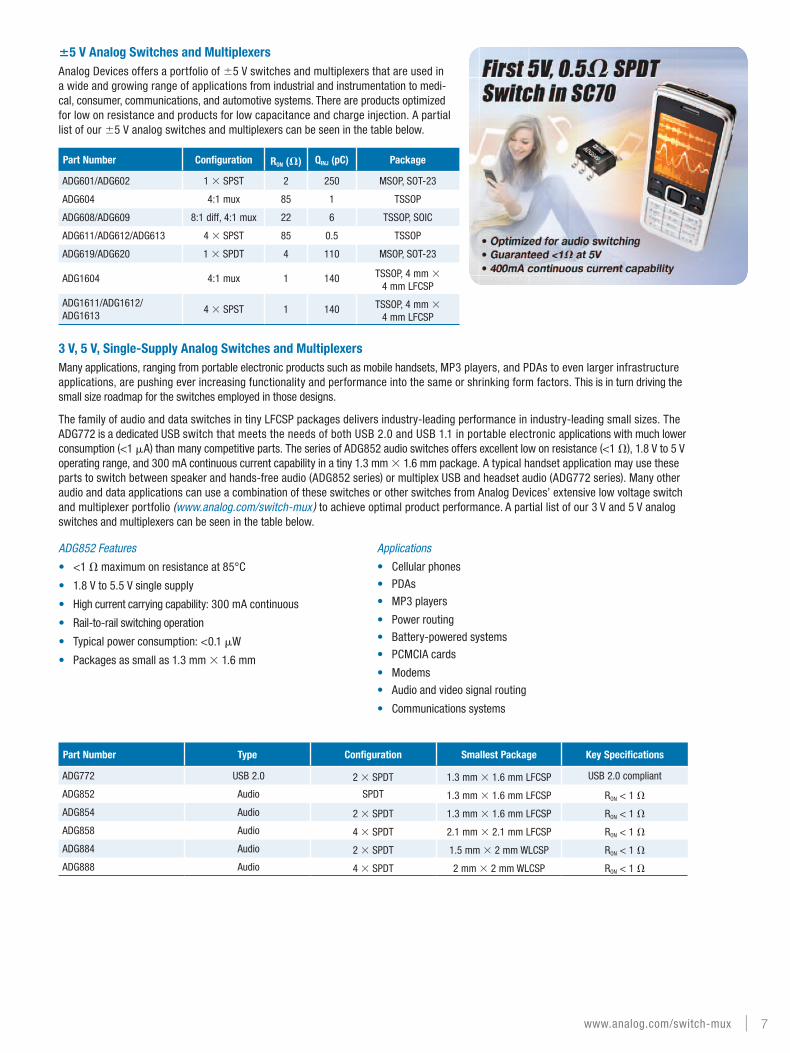
3 V, 5 V, Single-Supply Analog Switches and MultiplexersMany applications, ranging from portable electronic products such as mobile handsets, MP3 players, and PDAs to even larger infrastructure applications, are pushing ever increasing functionality and performance into the same or shrinking form factors. This is in turn driving the small size roadmap for the switches employed in those designs.
The family of audio and data switches in tiny LFCSP packages delivers industry-leading performance in industry-leading small sizes. The ADG772 is a dedicated USB switch that meets the needs of both USB 2.0 and USB 1.1 in portable electronic applications with much lower consumption (<1 μA) than many competitive parts. The series of ADG852 audio switches offers excellent low on resistance (<1 Ω), 1.8 V to 5 V operating range, and 300 mA continuous current capability in a tiny 1.3 mm × 1.6 mm package. A typical handset application may use these parts to switch between speaker and hands-free audio (ADG852 series) or multiplex USB and headset audio (ADG772 series). Many other audio and data applications can use a combination of these switches or other switches from Analog Devices’ extensive low voltage switch and multiplexer portfolio (www.analog.com/switch-mux ) to achieve optimal product performance. A partial list of our 3 V and 5 V analog switches and multiplexers can be seen in the table below.
ADG852 Features
• <1 Ω maximum on resistance at 85°C
• 1.8 V to 5.5 V single supply
• High current carrying capability: 300 mA continuous
• Rail-to-rail switching operation
• Typical power consumption: <0.1 μW
• Packages as small as 1.3 mm × 1.6 mm
Applications
• Cellular phones
• PDAs
• MP3 players
• Power routing
• Battery-powered systems
• PCMCIA cards
• Modems
• Audio and video signal routing
• Communications systems
Part number Type Configuration Smallest Package Key Specifications
ADG772 USB 2.0 2 × SPDT 1.3 mm × 1.6 mm LFCSP USB 2.0 compliant
ADG852 Audio SPDT 1.3 mm × 1.6 mm LFCSP RON < 1 ΩADG854 Audio 2 × SPDT 1.3 mm × 1.6 mm LFCSP RON < 1 ΩADG858 Audio 4 × SPDT 2.1 mm × 2.1 mm LFCSP RON < 1 ΩADG884 Audio 2 × SPDT 1.5 mm × 2 mm WLCSP RON < 1 ΩADG888 Audio 4 × SPDT 2 mm × 2 mm WLCSP RON < 1 Ω
www.analog.com/switch-mux | 7
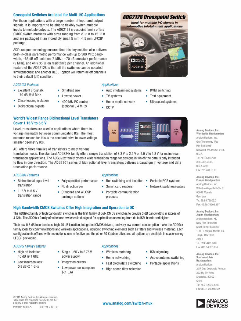
Crosspoint Switches Are Ideal for Multi-I/o ApplicationsFor those applications with a large number of input and output signals, it is important to be able to flexibly switch multiple inputs to multiple outputs. The ADG2128 crosspoint family offers CMOS switch matrices with sizes ranging from 8 × 8 to 12 × 8 and are packaged in an incredibly small 5 mm × 5 mm LFCSP package.
ADI’s unique technology ensures that this tiny solution also delivers best-in-class parametric performance with up to 300 MHz band-width, –65 dB off isolation (5 MHz), –70 dB crosstalk performance (5 MHz), and only 35 Ω on resistance per channel. An additional feature of the ADG2128 is that all the switches can be updated simultaneously, and another RESET option will return all off channels to their default (off) condition.
ADG2128 Features
• Excellent crosstalk: –70 dB @ 5 MHz
• Class-leading isolation
• Bidirectional signals
• Smallest size
• Lowest power
• 400 kHz I2C control (optional 3.4 MHz)
Applications
• Auto infotainment systems
• TV systems
• Home media network
• CCTV
• KVM switching
• Test equipment
• Ultrasound systems
World’s Widest Range Bidirectional Level Translators Cover 1.15 V to 5.5 VLevel translators are used in applications where there is a voltage mismatch between communicating ICs. The most common reason for this is the constant drive to lower voltage, smaller geometry ICs.
ADI offers three families of translators to meet various translation needs. The standard ADG324x family offers simple translation of 3.3 V to 2.5 V or 2.5 V to 1.8 V for mainstream translation applications. The ADG323x family offers a wide translation range for designs in which the data is only intended to flow in one direction. The ADG3301 series of bidirectional level translators delivers a paradigm in voltage and data translation performance.
ADG3301 Features
• Bidirectional logic level translation
• 1.15 V to 5.5 V translation range
• Fully specified performance
• No direction pin
• Standard and WLCSP package options
Applications
• Bus switching and isolation
• Smart card readers
• Portable communication products
• Portable POS systems
• Network switches/routers
High Bandwidth CMoS Switches offer High Integration and operation to dCThe ADG9xx family of high bandwidth switches is the first family of bulk CMOS switches to provide 3 dB bandwidths in excess of 4 GHz. The ADG9xx family of wideband switches is designed for applications operating from dc to ISM bands and higher.
Their low 0.8 dB insertion loss, high 40 dB isolation, integrated CMOS drivers, and very low current consumption make the ADG9xx family ideal for communications and wireless applications, including switching elements such as filters and wireless metering. Each configuration is offered with two options, one reflective and the other 50 Ω absorptive, and all options are available in space-saving LFCSP packaging.
ADG9xx Family Features
• High off isolation: 40 dB @ 1 GHz
• Low insertion loss: 0.8 dB @ 1 GHz
• Single 1.65 V to 2.75 V power supply
• Integrated drivers
• Low power consumption (<1 μA)
Applications
• Wireless metering
• Home networking
• Fast clock/data switching
• High speed filter selection
• ISM signaling
• Active antenna switching
• Portable applications
www.analog.com/switch-mux
Analog Devices, Inc.Worldwide HeadquartersAnalog Devices, Inc. One Technology Way P.O. Box 9106 Norwood, MA 02062-9106 U.S.A. Tel: 781.329.4700 (800.262.5643, U.S.A. only) Fax: 781.461.3113
Analog Devices, Inc. Europe HeadquartersAnalog Devices, Inc. Wilhelm-Wagenfeld-Str. 6 80807 Munich Germany Tel: 49.89.76903.0 Fax: 49.89.76903.157
Analog Devices, Inc. Japan HeadquartersAnalog Devices, KK New Pier Takeshiba South Tower Building 1-16-1 Kaigan, Minato-ku, Tokyo, 105-6891 Japan Tel: 813.5402.8200 Fax: 813.5402.1064
Analog Devices, Inc. Southeast Asia HeadquartersAnalog Devices 22/F One Corporate Avenue 222 Hu Bin Road Shanghai, 200021 China Tel: 86.21.2320.8000 Fax: 86.21.2320.8222
©2011 Analog Devices, Inc. All rights reserved. Trademarks and registered trademarks are the property of their respective owners.
Printed in the U.S.A. BR07745-2-9/11(B)