Embed Size (px)
Citation preview
1. General description
The 74HC4052; 74HCT4052 is a high-speed Si-gate CMOS device and is pin compatible with the HEF4052B. The device is specified in compliance with JEDEC standard no. 7A.
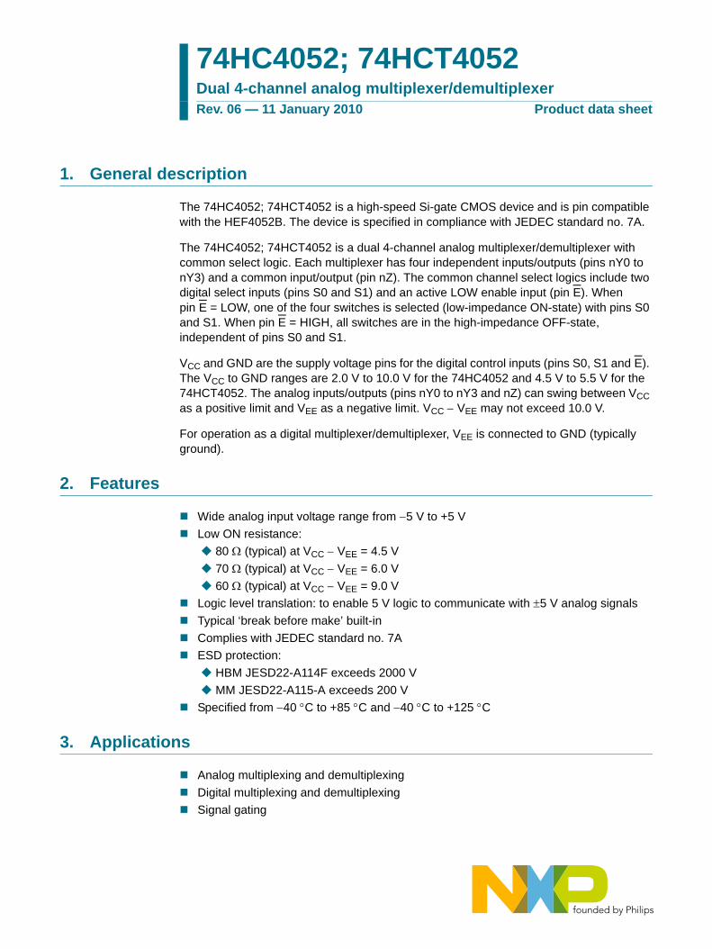
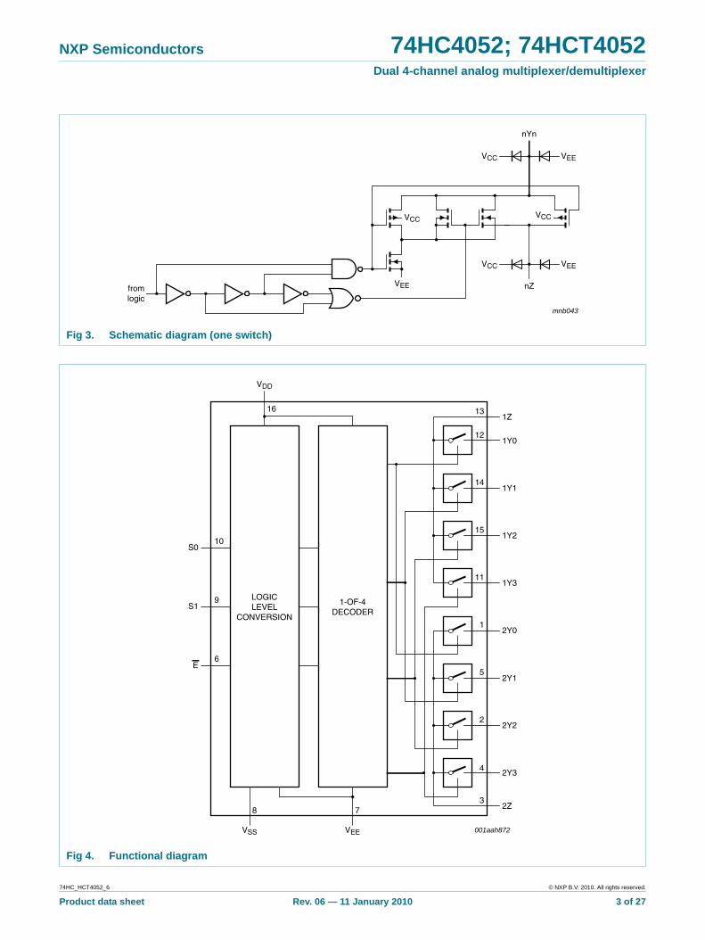
The 74HC4052; 74HCT4052 is a dual 4-channel analog multiplexer/demultiplexer with common select logic. Each multiplexer has four independent inputs/outputs (pins nY0 to nY3) and a common input/output (pin nZ). The common channel select logics include two digital select inputs (pins S0 and S1) and an active LOW enable input (pin E). When pin E = LOW, one of the four switches is selected (low-impedance ON-state) with pins S0 and S1. When pin E = HIGH, all switches are in the high-impedance OFF-state, independent of pins S0 and S1.
VCC and GND are the supply voltage pins for the digital control inputs (pins S0, S1 and E). The VCC to GND ranges are 2.0 V to 10.0 V for the 74HC4052 and 4.5 V to 5.5 V for the 74HCT4052. The analog inputs/outputs (pins nY0 to nY3 and nZ) can swing between VCC as a positive limit and VEE as a negative limit. VCC − VEE may not exceed 10.0 V.
For operation as a digital multiplexer/demultiplexer, VEE is connected to GND (typically ground).
2. Features
Wide analog input voltage range from −5 V to +5 VLow ON resistance:
80 Ω (typical) at VCC − VEE = 4.5 V70 Ω (typical) at VCC − VEE = 6.0 V60 Ω (typical) at VCC − VEE = 9.0 V
Logic level translation: to enable 5 V logic to communicate with ±5 V analog signalsTypical ‘break before make’ built-inComplies with JEDEC standard no. 7AESD protection:
HBM JESD22-A114F exceeds 2000 VMM JESD22-A115-A exceeds 200 V
Specified from −40 °C to +85 °C and −40 °C to +125 °C
3. Applications
Analog multiplexing and demultiplexingDigital multiplexing and demultiplexingSignal gating
74HC4052; 74HCT4052Dual 4-channel analog multiplexer/demultiplexerRev. 06 — 11 January 2010 Product data sheet
NXP Semiconductors 74HC4052; 74HCT4052Dual 4-channel analog multiplexer/demultiplexer
4. Ordering information
5. Functional diagram
Table 1. Ordering information Type number Package
Temperature range Name Description Version74HC405274HC4052D −40 °C to +125 °C SO16 plastic small outline package; 16 leads; body
width 3.9 mmSOT109-1
74HC4052DB −40 °C to +125 °C SSOP16 plastic shrink small outline package; 16 leads; body width 5.3 mm
SOT338-1
74HC4052N −40 °C to +125 °C DIP16 plastic dual in-line package; 16 leads (300 mil) SOT38-4
74HC4052PW −40 °C to +125 °C TSSOP16 plastic thin shrink small outline package; 16 leads; body width 4.4 mm
SOT403-1
74HC4052BQ −40 °C to +125 °C DHVQFN16 plastic dual-in line compatible thermal enhanced very thin quad flat package; no leads; 16 terminals; body 2.5 × 3.5 × 0.85 mm
SOT763-1
74HCT405274HCT4052D −40 °C to +125 °C SO16 plastic small outline package; 16 leads; body
width 3.9 mmSOT109-1
74HCT4052DB −40 °C to +125 °C SSOP16 plastic shrink small outline package; 16 leads; body width 5.3 mm
SOT338-1
74HCT4052N −40 °C to +125 °C DIP16 plastic dual in-line package; 16 leads (300 mil) SOT38-4
74HCT4052PW −40 °C to +125 °C TSSOP16 plastic thin shrink small outline package; 16 leads; body width 4.4 mm
SOT403-1
74HCT4052BQ −40 °C to +125 °C DHVQFN16 plastic dual-in line compatible thermal enhanced very thin quad flat package; no leads; 16 terminals; body 2.5 × 3.5 × 0.85 mm
SOT763-1
Fig 1. Logic symbol Fig 2. IEC logic symbol
001aah824
1Z
13
S0
S1
E
10
9
6
2Z
3
2Y3
2Y2
2Y1
2Y0
1Y3
1Y2
1Y1
1Y0
4
2
5
1
11
15
14
12
001aah825
1
0
G4
MDX
03
4 ×
3
2
1
0
4
2
5
1
11
15
14
12
10
9
6
3
13
74HC_HCT4052_6 © NXP B.V. 2010. All rights reserved.
Product data sheet Rev. 06 — 11 January 2010 2 of 27
NXP Semiconductors 74HC4052; 74HCT4052Dual 4-channel analog multiplexer/demultiplexer
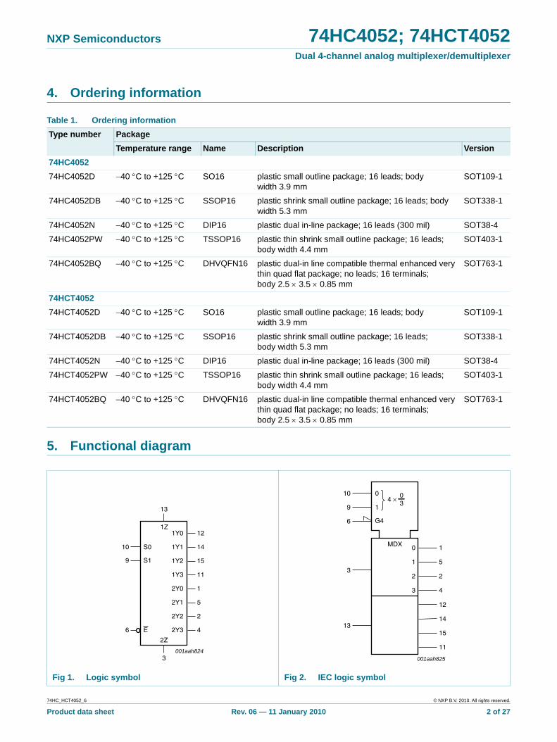
Fig 3. Schematic diagram (one switch)
mnb043
fromlogic
VCC
VEE
VEE
VCC
VCC
VEE
nYn
nZ
VCC
Fig 4. Functional diagram
001aah872
1-OF-4DECODER
LOGICLEVEL
CONVERSION
78
VEEVSS
VDD
12
1316
3
14
15
11
10
9
6
S0
S1
E
1
5
2
1Y0
1Z
2Z
1Y1
1Y2
1Y3
2Y0
2Y1
2Y2
2Y34
74HC_HCT4052_6 © NXP B.V. 2010. All rights reserved.
Product data sheet Rev. 06 — 11 January 2010 3 of 27
NXP Semiconductors 74HC4052; 74HCT4052Dual 4-channel analog multiplexer/demultiplexer
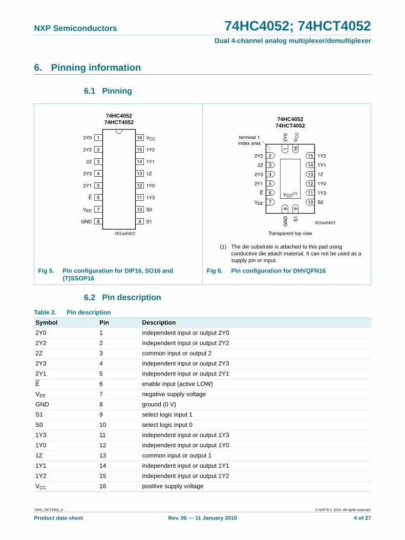
6. Pinning information
6.1 Pinning
6.2 Pin description
(1) The die substrate is attached to this pad using conductive die attach material. It can not be used as a supply pin or input.
Fig 5. Pin configuration for DIP16, SO16 and (T)SSOP16
Fig 6. Pin configuration for DHVQFN16
74HC405274HCT4052
2Y0 VCC
2Y2 1Y2
2Z 1Y1
2Y3 1Z
2Y1 1Y0
E 1Y3
VEE S0
GND S1
001aah822
1
2
3
4
5
6
7
8
10
9
12
11
14
13
16
15
001aah823
74HC405274HCT4052
VEE
VCC(1)
S0
E 1Y3
2Y1 1Y0
2Y3 1Z
2Z 1Y1
2Y2 1Y2
GN
D S1
2Y0
VC
C
Transparent top view
7 10
6 11
5 12
4 13
3 14
2 15
8 9
1 16
terminal 1index area
Table 2. Pin description Symbol Pin Description2Y0 1 independent input or output 2Y0
2Y2 2 independent input or output 2Y2
2Z 3 common input or output 2
2Y3 4 independent input or output 2Y3
2Y1 5 independent input or output 2Y1
E 6 enable input (active LOW)
VEE 7 negative supply voltage
GND 8 ground (0 V)
S1 9 select logic input 1
S0 10 select logic input 0
1Y3 11 independent input or output 1Y3
1Y0 12 independent input or output 1Y0
1Z 13 common input or output 1
1Y1 14 independent input or output 1Y1
1Y2 15 independent input or output 1Y2
VCC 16 positive supply voltage
74HC_HCT4052_6 © NXP B.V. 2010. All rights reserved.
Product data sheet Rev. 06 — 11 January 2010 4 of 27
NXP Semiconductors 74HC4052; 74HCT4052Dual 4-channel analog multiplexer/demultiplexer
7. Functional description
7.1 Function table
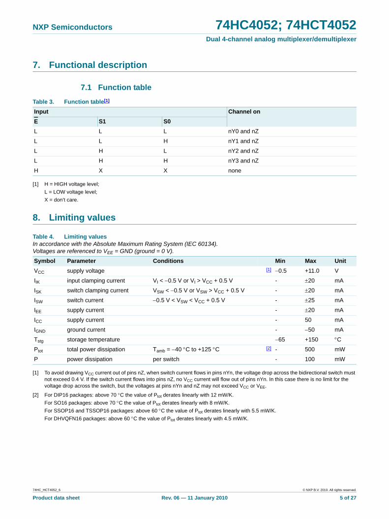
[1] H = HIGH voltage level;L = LOW voltage level;X = don’t care.
8. Limiting values
[1] To avoid drawing VCC current out of pins nZ, when switch current flows in pins nYn, the voltage drop across the bidirectional switch must not exceed 0.4 V. If the switch current flows into pins nZ, no VCC current will flow out of pins nYn. In this case there is no limit for the voltage drop across the switch, but the voltages at pins nYn and nZ may not exceed VCC or VEE.
[2] For DIP16 packages: above 70 °C the value of Ptot derates linearly with 12 mW/K.For SO16 packages: above 70 °C the value of Ptot derates linearly with 8 mW/K.For SSOP16 and TSSOP16 packages: above 60 °C the value of Ptot derates linearly with 5.5 mW/K.For DHVQFN16 packages: above 60 °C the value of Ptot derates linearly with 4.5 mW/K.
Table 3. Function table[1] Input Channel onE S1 S0L L L nY0 and nZ
L L H nY1 and nZ
L H L nY2 and nZ
L H H nY3 and nZ
H X X none
Table 4. Limiting values In accordance with the Absolute Maximum Rating System (IEC 60134).Voltages are referenced to VEE = GND (ground = 0 V).
Symbol Parameter Conditions Min Max UnitVCC supply voltage [1] −0.5 +11.0 V
IIK input clamping current VI < −0.5 V or VI > VCC + 0.5 V - ±20 mA
ISK switch clamping current VSW < −0.5 V or VSW > VCC + 0.5 V - ±20 mA
ISW switch current −0.5 V < VSW < VCC + 0.5 V - ±25 mA
IEE supply current - ±20 mA
ICC supply current - 50 mA
IGND ground current - −50 mA
Tstg storage temperature −65 +150 °C
Ptot total power dissipation Tamb = −40 °C to +125 °C [2] - 500 mW
P power dissipation per switch - 100 mW
74HC_HCT4052_6 © NXP B.V. 2010. All rights reserved.
Product data sheet Rev. 06 — 11 January 2010 5 of 27
NXP Semiconductors 74HC4052; 74HCT4052Dual 4-channel analog multiplexer/demultiplexer
9. Recommended operating conditions
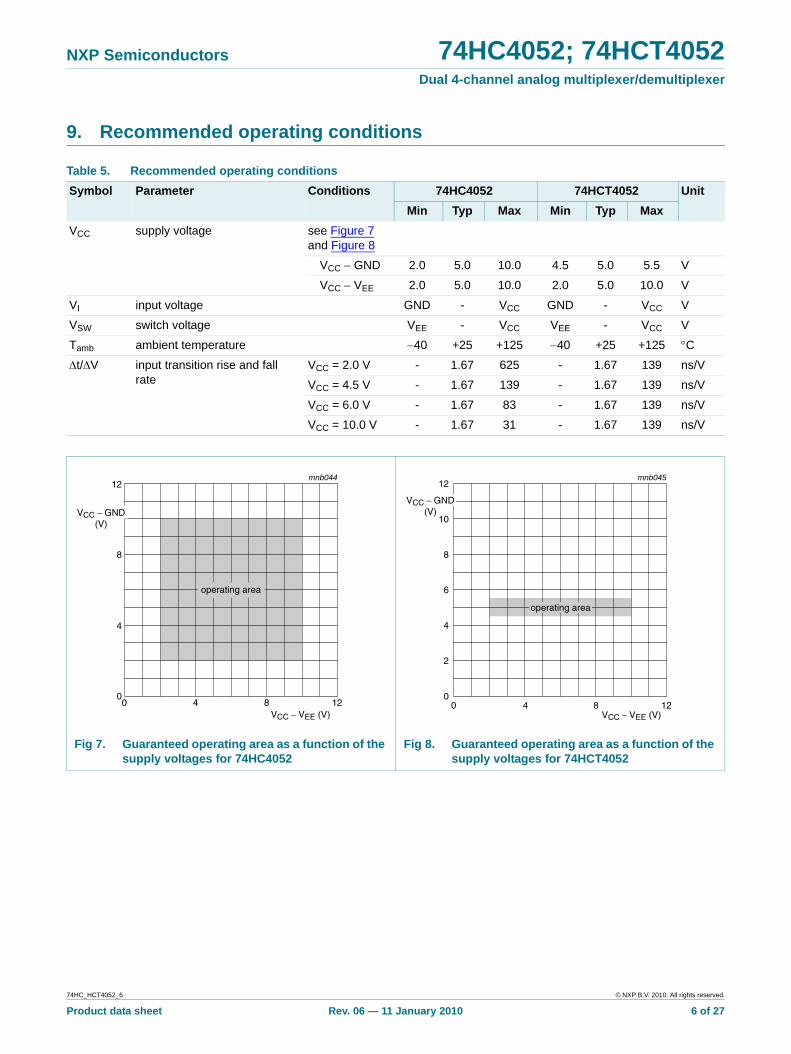
Table 5. Recommended operating conditions Symbol Parameter Conditions 74HC4052 74HCT4052 Unit
Min Typ Max Min Typ MaxVCC supply voltage see Figure 7
and Figure 8
VCC − GND 2.0 5.0 10.0 4.5 5.0 5.5 V
VCC − VEE 2.0 5.0 10.0 2.0 5.0 10.0 V
VI input voltage GND - VCC GND - VCC V
VSW switch voltage VEE - VCC VEE - VCC V
Tamb ambient temperature −40 +25 +125 −40 +25 +125 °C
Δt/ΔV input transition rise and fall rate
VCC = 2.0 V - 1.67 625 - 1.67 139 ns/V
VCC = 4.5 V - 1.67 139 - 1.67 139 ns/V
VCC = 6.0 V - 1.67 83 - 1.67 139 ns/V
VCC = 10.0 V - 1.67 31 - 1.67 139 ns/V
Fig 7. Guaranteed operating area as a function of the supply voltages for 74HC4052
Fig 8. Guaranteed operating area as a function of the supply voltages for 74HCT4052
mnb044
0 4 12
12
0
4
8
8
operating area
VCC − VEE (V)
VCC − GND(V)
mnb045
0
12
6
10
8
2
4
0 4 128
operating area
VCC − VEE (V)
VCC − GND(V)
74HC_HCT4052_6 © NXP B.V. 2010. All rights reserved.
Product data sheet Rev. 06 — 11 January 2010 6 of 27
NXP Semiconductors 74HC4052; 74HCT4052Dual 4-channel analog multiplexer/demultiplexer
10. Static characteristics
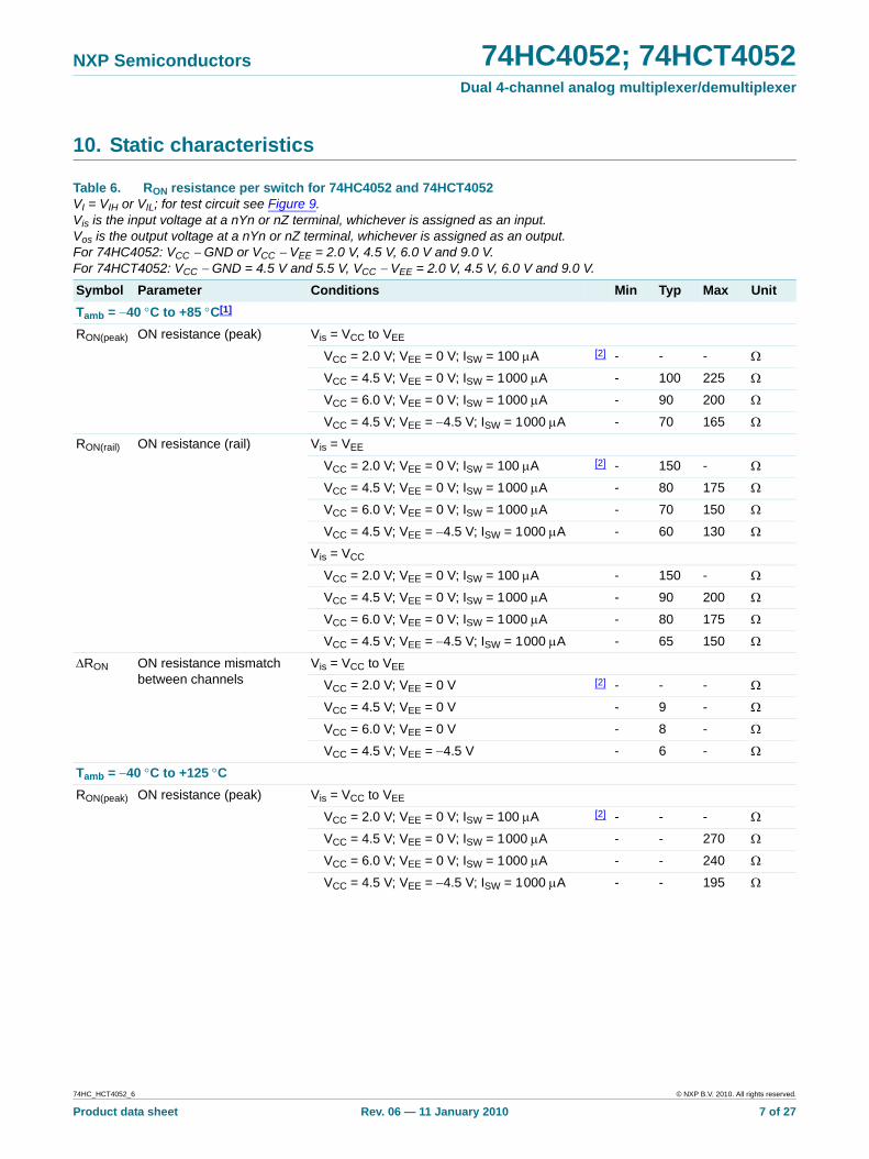
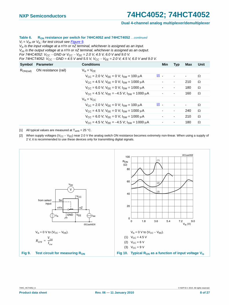
Table 6. RON resistance per switch for 74HC4052 and 74HCT4052 VI = VIH or VIL; for test circuit see Figure 9. Vis is the input voltage at a nYn or nZ terminal, whichever is assigned as an input.Vos is the output voltage at a nYn or nZ terminal, whichever is assigned as an output.For 74HC4052: VCC − GND or VCC − VEE = 2.0 V, 4.5 V, 6.0 V and 9.0 V.For 74HCT4052: VCC − GND = 4.5 V and 5.5 V, VCC − VEE = 2.0 V, 4.5 V, 6.0 V and 9.0 V.
Symbol Parameter Conditions Min Typ Max UnitTamb = −40 °C to +85 °C[1]
RON(peak) ON resistance (peak) Vis = VCC to VEE
VCC = 2.0 V; VEE = 0 V; ISW = 100 μA [2] - - - Ω
VCC = 4.5 V; VEE = 0 V; ISW = 1 000 μA - 100 225 Ω
VCC = 6.0 V; VEE = 0 V; ISW = 1 000 μA - 90 200 Ω
VCC = 4.5 V; VEE = −4.5 V; ISW = 1 000 μA - 70 165 Ω
RON(rail) ON resistance (rail) Vis = VEE
VCC = 2.0 V; VEE = 0 V; ISW = 100 μA [2] - 150 - Ω
VCC = 4.5 V; VEE = 0 V; ISW = 1 000 μA - 80 175 Ω
VCC = 6.0 V; VEE = 0 V; ISW = 1 000 μA - 70 150 Ω
VCC = 4.5 V; VEE = −4.5 V; ISW = 1 000 μA - 60 130 Ω
Vis = VCC
VCC = 2.0 V; VEE = 0 V; ISW = 100 μA - 150 - Ω
VCC = 4.5 V; VEE = 0 V; ISW = 1 000 μA - 90 200 Ω
VCC = 6.0 V; VEE = 0 V; ISW = 1 000 μA - 80 175 Ω
VCC = 4.5 V; VEE = −4.5 V; ISW = 1 000 μA - 65 150 Ω
ΔRON ON resistance mismatch between channels
Vis = VCC to VEE
VCC = 2.0 V; VEE = 0 V [2] - - - Ω
VCC = 4.5 V; VEE = 0 V - 9 - Ω
VCC = 6.0 V; VEE = 0 V - 8 - Ω
VCC = 4.5 V; VEE = −4.5 V - 6 - Ω
Tamb = −40 °C to +125 °CRON(peak) ON resistance (peak) Vis = VCC to VEE
VCC = 2.0 V; VEE = 0 V; ISW = 100 μA [2] - - - Ω
VCC = 4.5 V; VEE = 0 V; ISW = 1 000 μA - - 270 Ω
VCC = 6.0 V; VEE = 0 V; ISW = 1 000 μA - - 240 Ω
VCC = 4.5 V; VEE = −4.5 V; ISW = 1 000 μA - - 195 Ω
74HC_HCT4052_6 © NXP B.V. 2010. All rights reserved.
Product data sheet Rev. 06 — 11 January 2010 7 of 27
NXP Semiconductors 74HC4052; 74HCT4052Dual 4-channel analog multiplexer/demultiplexer
[1] All typical values are measured at Tamb = 25 °C.
[2] When supply voltages (VCC − VEE) near 2.0 V the analog switch ON resistance becomes extremely non-linear. When using a supply of 2 V, it is recommended to use these devices only for transmitting digital signals.
RON(rail) ON resistance (rail) Vis = VEE
VCC = 2.0 V; VEE = 0 V; ISW = 100 μA [2] - - - Ω
VCC = 4.5 V; VEE = 0 V; ISW = 1 000 μA - - 210 Ω
VCC = 6.0 V; VEE = 0 V; ISW = 1 000 μA - - 180 Ω
VCC = 4.5 V; VEE = −4.5 V; ISW = 1 000 μA - - 160 Ω
Vis = VCC
VCC = 2.0 V; VEE = 0 V; ISW = 100 μA [2] - - - Ω
VCC = 4.5 V; VEE = 0 V; ISW = 1 000 μA - - 240 Ω
VCC = 6.0 V; VEE = 0 V; ISW = 1 000 μA - - 210 Ω
VCC = 4.5 V; VEE = −4.5 V; ISW = 1 000 μA - - 180 Ω
Table 6. RON resistance per switch for 74HC4052 and 74HCT4052 …continuedVI = VIH or VIL; for test circuit see Figure 9. Vis is the input voltage at a nYn or nZ terminal, whichever is assigned as an input.Vos is the output voltage at a nYn or nZ terminal, whichever is assigned as an output.For 74HC4052: VCC − GND or VCC − VEE = 2.0 V, 4.5 V, 6.0 V and 9.0 V.For 74HCT4052: VCC − GND = 4.5 V and 5.5 V, VCC − VEE = 2.0 V, 4.5 V, 6.0 V and 9.0 V.
Symbol Parameter Conditions Min Typ Max Unit
Vis = 0 V to (VCC − VEE). Vis = 0 V to (VCC − VEE).(1) VCC = 4.5 V(2) VCC = 6 V(3) VCC = 9 V
Fig 9. Test circuit for measuring RON Fig 10. Typical RON as a function of input voltage Vis
V
001aah826
nYn
Snfrom selectinput
nZ
GND VEE
VCC
Vis Isw
Vsw
Vis (V)0 9.07.23.6 5.41.8
001aai068
40
60
20
80
100
RON(Ω)
0
(1)
(2)
(3)
RONVswIsw---------=
74HC_HCT4052_6 © NXP B.V. 2010. All rights reserved.
Product data sheet Rev. 06 — 11 January 2010 8 of 27
NXP Semiconductors 74HC4052; 74HCT4052Dual 4-channel analog multiplexer/demultiplexer
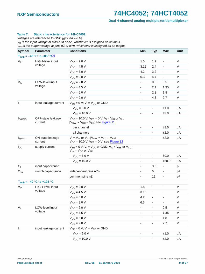
Table 7. Static characteristics for 74HC4052 Voltages are referenced to GND (ground = 0 V).Vis is the input voltage at pins nYn or nZ, whichever is assigned as an input.Vos is the output voltage at pins nZ or nYn, whichever is assigned as an output.
Symbol Parameter Conditions Min Typ Max UnitTamb = −40 °C to +85 °C[1]
VIH HIGH-level input voltage
VCC = 2.0 V 1.5 1.2 - V
VCC = 4.5 V 3.15 2.4 - V
VCC = 6.0 V 4.2 3.2 - V
VCC = 9.0 V 6.3 4.7 - V
VIL LOW-level input voltage
VCC = 2.0 V - 0.8 0.5 V
VCC = 4.5 V - 2.1 1.35 V
VCC = 6.0 V - 2.8 1.8 V
VCC = 9.0 V - 4.3 2.7 V
II input leakage current VEE = 0 V; VI = VCC or GND
VCC = 6.0 V - - ±1.0 μA
VCC = 10.0 V - - ±2.0 μA
IS(OFF) OFF-state leakage current
VCC = 10.0 V; VEE = 0 V; VI = VIH or VIL; |VSW| = VCC − VEE; see Figure 11
per channel - - ±1.0 μA
all channels - - ±2.0 μA
IS(ON) ON-state leakage current
VI = VIH or VIL; |VSW| = VCC − VEE; VCC = 10.0 V; VEE = 0 V; see Figure 12
- - ±2.0 μA
ICC supply current VEE = 0 V; VI = VCC or GND; Vis = VEE or VCC; Vos = VCC or VEE
VCC = 6.0 V - - 80.0 μA
VCC = 10.0 V - - 160.0 μA
CI input capacitance - 3.5 - pF
Csw switch capacitance independent pins nYn - 5 - pF
common pins nZ - 12 - pF
Tamb = −40 °C to +125 °CVIH HIGH-level input
voltageVCC = 2.0 V 1.5 - - V
VCC = 4.5 V 3.15 - - V
VCC = 6.0 V 4.2 - - V
VCC = 9.0 V 6.3 - - V
VIL LOW-level input voltage
VCC = 2.0 V - - 0.5 V
VCC = 4.5 V - - 1.35 V
VCC = 6.0 V - - 1.8 V
VCC = 9.0 V - - 2.7 V
II input leakage current VEE = 0 V; VI = VCC or GND
VCC = 6.0 V - - ±1.0 μA
VCC = 10.0 V - - ±2.0 μA
74HC_HCT4052_6 © NXP B.V. 2010. All rights reserved.
Product data sheet Rev. 06 — 11 January 2010 9 of 27
NXP Semiconductors 74HC4052; 74HCT4052Dual 4-channel analog multiplexer/demultiplexer
[1] All typical values are measured at Tamb = 25 °C.
IS(OFF) OFF-state leakage current
VCC = 10.0 V; VEE = 0 V; VI = VIH or VIL; |VSW| = VCC − VEE; see Figure 11
per channel - - ±1.0 μA
all channels - - ±2.0 μA
IS(ON) ON-state leakage current
VI = VIH or VIL; |VSW| = VCC − VEE; VCC = 10.0 V; VEE = 0 V; see Figure 12
- - ±2.0 μA
ICC supply current VEE = 0 V; VI = VCC or GND; Vis = VEE or VCC; Vos = VCC or VEE
VCC = 6.0 V - - 160.0 μA
VCC = 10.0 V - - 320.0 μA
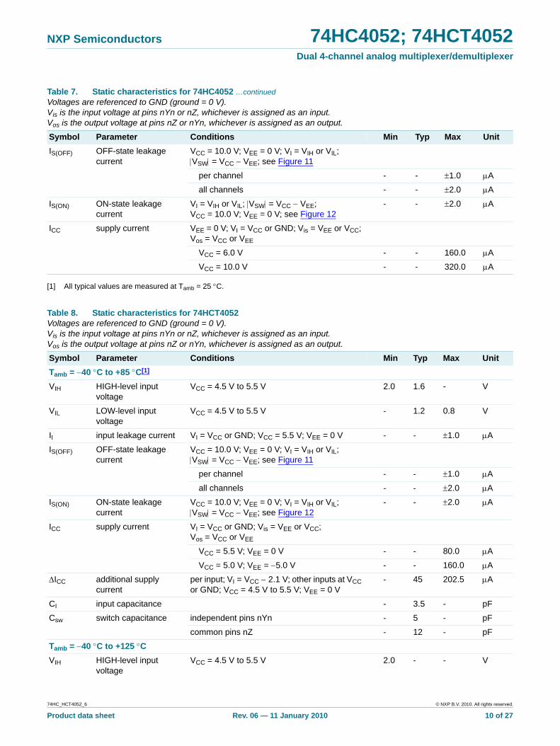
Table 7. Static characteristics for 74HC4052 …continuedVoltages are referenced to GND (ground = 0 V).Vis is the input voltage at pins nYn or nZ, whichever is assigned as an input.Vos is the output voltage at pins nZ or nYn, whichever is assigned as an output.
Symbol Parameter Conditions Min Typ Max Unit
Table 8. Static characteristics for 74HCT4052 Voltages are referenced to GND (ground = 0 V).Vis is the input voltage at pins nYn or nZ, whichever is assigned as an input.Vos is the output voltage at pins nZ or nYn, whichever is assigned as an output.
Symbol Parameter Conditions Min Typ Max UnitTamb = −40 °C to +85 °C[1]
VIH HIGH-level input voltage
VCC = 4.5 V to 5.5 V 2.0 1.6 - V
VIL LOW-level input voltage
VCC = 4.5 V to 5.5 V - 1.2 0.8 V
II input leakage current VI = VCC or GND; VCC = 5.5 V; VEE = 0 V - - ±1.0 μA
IS(OFF) OFF-state leakage current
VCC = 10.0 V; VEE = 0 V; VI = VIH or VIL; |VSW| = VCC − VEE; see Figure 11
per channel - - ±1.0 μA
all channels - - ±2.0 μA
IS(ON) ON-state leakage current
VCC = 10.0 V; VEE = 0 V; VI = VIH or VIL; |VSW| = VCC − VEE; see Figure 12
- - ±2.0 μA
ICC supply current VI = VCC or GND; Vis = VEE or VCC; Vos = VCC or VEE
VCC = 5.5 V; VEE = 0 V - - 80.0 μA
VCC = 5.0 V; VEE = −5.0 V - - 160.0 μA
ΔICC additional supply current
per input; VI = VCC − 2.1 V; other inputs at VCC or GND; VCC = 4.5 V to 5.5 V; VEE = 0 V
- 45 202.5 μA
CI input capacitance - 3.5 - pF
Csw switch capacitance independent pins nYn - 5 - pF
common pins nZ - 12 - pF
Tamb = −40 °C to +125 °CVIH HIGH-level input
voltageVCC = 4.5 V to 5.5 V 2.0 - - V
74HC_HCT4052_6 © NXP B.V. 2010. All rights reserved.
Product data sheet Rev. 06 — 11 January 2010 10 of 27
NXP Semiconductors 74HC4052; 74HCT4052Dual 4-channel analog multiplexer/demultiplexer
[1] All typical values are measured at Tamb = 25 °C.
VIL LOW-level input voltage
VCC = 4.5 V to 5.5 V - - 0.8 V
ILI input leakage current VI = VCC or GND; VCC = 5.5 V; VEE = 0 V - - ±1.0 μA
IS(OFF) OFF-state leakage current
VCC = 10.0 V; VEE = 0 V; VI = VIH or VIL; |VSW| = VCC − VEE; see Figure 11
per channel - - ±1.0 μA
all channels - - ±2.0 μA
IS(ON) ON-state leakage current
VCC = 10.0 V; VEE = 0 V; VI = VIH or VIL; |VSW| = VCC − VEE; see Figure 12
- - ±2.0 μA
ICC supply current VI = VCC or GND; Vis = VEE or VCC; Vos = VCC or VEE
VCC = 5.5 V; VEE = 0 V - - 160.0 μA
VCC = 5.0 V; VEE = −5.0 V - - 320.0 μA
ΔICC additional supply current
per input; VI = VCC − 2.1 V; other inputs at VCC or GND; VCC = 4.5 V to 5.5 V; VEE = 0 V
- - 220.5 μA
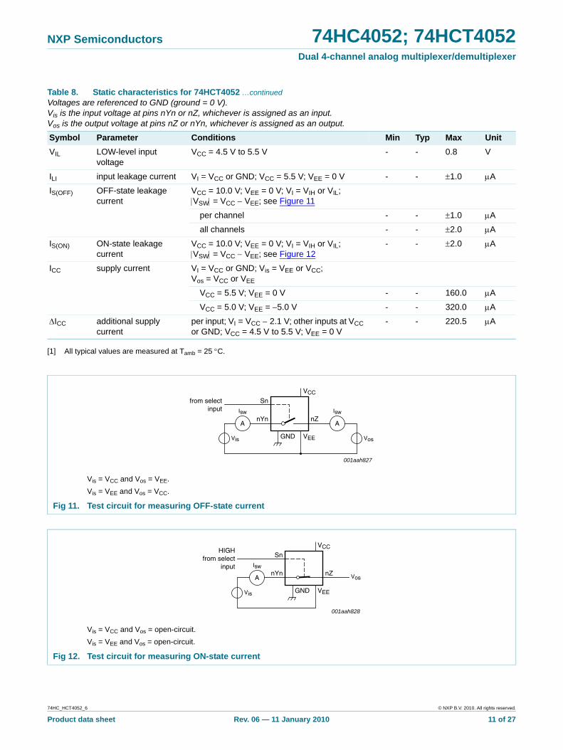
Table 8. Static characteristics for 74HCT4052 …continuedVoltages are referenced to GND (ground = 0 V).Vis is the input voltage at pins nYn or nZ, whichever is assigned as an input.Vos is the output voltage at pins nZ or nYn, whichever is assigned as an output.
Symbol Parameter Conditions Min Typ Max Unit
Vis = VCC and Vos = VEE.Vis = VEE and Vos = VCC.
Fig 11. Test circuit for measuring OFF-state current
001aah827
nYn
Snfrom selectinput
nZ
GND VEE
VCC
Vis Vos
Isw
A
Isw
A
Vis = VCC and Vos = open-circuit.Vis = VEE and Vos = open-circuit.
Fig 12. Test circuit for measuring ON-state current
Isw
A
001aah828
nYn
SnHIGH
from selectinput
nZ
GND VEE
VCC
Vis
Vos
74HC_HCT4052_6 © NXP B.V. 2010. All rights reserved.
Product data sheet Rev. 06 — 11 January 2010 11 of 27
NXP Semiconductors 74HC4052; 74HCT4052Dual 4-channel analog multiplexer/demultiplexer
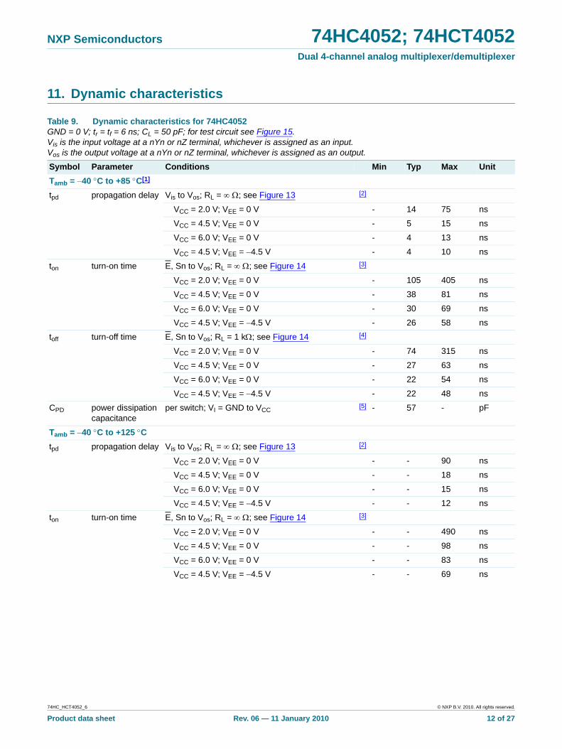
11. Dynamic characteristics
Table 9. Dynamic characteristics for 74HC4052 GND = 0 V; tr = tf = 6 ns; CL = 50 pF; for test circuit see Figure 15.Vis is the input voltage at a nYn or nZ terminal, whichever is assigned as an input.Vos is the output voltage at a nYn or nZ terminal, whichever is assigned as an output.
Symbol Parameter Conditions Min Typ Max UnitTamb = −40 °C to +85 °C[1]
tpd propagation delay Vis to Vos; RL = ∞ Ω; see Figure 13 [2]
VCC = 2.0 V; VEE = 0 V - 14 75 ns
VCC = 4.5 V; VEE = 0 V - 5 15 ns
VCC = 6.0 V; VEE = 0 V - 4 13 ns
VCC = 4.5 V; VEE = −4.5 V - 4 10 ns
ton turn-on time E, Sn to Vos; RL = ∞ Ω; see Figure 14 [3]
VCC = 2.0 V; VEE = 0 V - 105 405 ns
VCC = 4.5 V; VEE = 0 V - 38 81 ns
VCC = 6.0 V; VEE = 0 V - 30 69 ns
VCC = 4.5 V; VEE = −4.5 V - 26 58 ns
toff turn-off time E, Sn to Vos; RL = 1 kΩ; see Figure 14 [4]
VCC = 2.0 V; VEE = 0 V - 74 315 ns
VCC = 4.5 V; VEE = 0 V - 27 63 ns
VCC = 6.0 V; VEE = 0 V - 22 54 ns
VCC = 4.5 V; VEE = −4.5 V - 22 48 ns
CPD power dissipation capacitance
per switch; VI = GND to VCC [5] - 57 - pF
Tamb = −40 °C to +125 °Ctpd propagation delay Vis to Vos; RL = ∞ Ω; see Figure 13 [2]
VCC = 2.0 V; VEE = 0 V - - 90 ns
VCC = 4.5 V; VEE = 0 V - - 18 ns
VCC = 6.0 V; VEE = 0 V - - 15 ns
VCC = 4.5 V; VEE = −4.5 V - - 12 ns
ton turn-on time E, Sn to Vos; RL = ∞ Ω; see Figure 14 [3]
VCC = 2.0 V; VEE = 0 V - - 490 ns
VCC = 4.5 V; VEE = 0 V - - 98 ns
VCC = 6.0 V; VEE = 0 V - - 83 ns
VCC = 4.5 V; VEE = −4.5 V - - 69 ns
74HC_HCT4052_6 © NXP B.V. 2010. All rights reserved.
Product data sheet Rev. 06 — 11 January 2010 12 of 27
NXP Semiconductors 74HC4052; 74HCT4052Dual 4-channel analog multiplexer/demultiplexer
[1] All typical values are measured at Tamb = 25 °C.
[2] tpd is the same as tPHL and tPLH.
[3] ton is the same as tPZH and tPZL.
[4] toff is the same as tPHZ and tPLZ.
[5] CPD is used to determine the dynamic power dissipation (PD in μW).PD = CPD × VCC2 × fi × N + Σ{(CL + Csw) × VCC2 × fo} where:fi = input frequency in MHz;fo = output frequency in MHz;N = number of inputs switching;Σ{(CL + Csw) × VCC2 × fo} = sum of outputs;CL = output load capacitance in pF;Csw = switch capacitance in pF;VCC = supply voltage in V.
toff turn-off time E, Sn to Vos; RL = 1 kΩ; see Figure 14 [4]
VCC = 2.0 V; VEE = 0 V - - 375 ns
VCC = 4.5 V; VEE = 0 V - - 75 ns
VCC = 6.0 V; VEE = 0 V - - 64 ns
VCC = 4.5 V; VEE = −4.5 V - - 57 ns
Table 9. Dynamic characteristics for 74HC4052 …continuedGND = 0 V; tr = tf = 6 ns; CL = 50 pF; for test circuit see Figure 15.Vis is the input voltage at a nYn or nZ terminal, whichever is assigned as an input.Vos is the output voltage at a nYn or nZ terminal, whichever is assigned as an output.
Symbol Parameter Conditions Min Typ Max Unit
Table 10. Dynamic characteristics for 74HCT4052 GND = 0 V; tr = tf = 6 ns; CL = 50 pF; for test circuit see Figure 15.Vis is the input voltage at a nYn or nZ terminal, whichever is assigned as an input.Vos is the output voltage at a nYn or nZ terminal, whichever is assigned as an output.
Symbol Parameter Conditions Min Typ Max UnitTamb = −40 °C to +85 °C[1]
tpd propagation delay Vis to Vos; RL = ∞ Ω; see Figure 13 [2]
VCC = 4.5 V; VEE = 0 V - 5 15 ns
VCC = 4.5 V; VEE = −4.5 V - 4 10 ns
ton turn-on time E, Sn to Vos; RL = 1 kΩ; see Figure 14 [3]
VCC = 4.5 V; VEE = 0 V - 41 88 ns
VCC = 4.5 V; VEE = −4.5 V - 28 60 ns
toff turn-off time E, Sn to Vos; RL = 1 kΩ; see Figure 14 [4]
VCC = 4.5 V; VEE = 0 V - 26 63 ns
VCC = 4.5 V; VEE = −4.5 V - 21 48 ns
CPD power dissipation capacitance
per switch; VI = GND to VCC − 1.5 V [5] - 57 - pF
Tamb = −40 °C to +125 °Ctpd propagation delay Vis to Vos; RL = ∞ Ω; see Figure 13 [2]
VCC = 4.5 V; VEE = 0 V - - 18 ns
VCC = 4.5 V; VEE = −4.5 V - - 12 ns
74HC_HCT4052_6 © NXP B.V. 2010. All rights reserved.
Product data sheet Rev. 06 — 11 January 2010 13 of 27
NXP Semiconductors 74HC4052; 74HCT4052Dual 4-channel analog multiplexer/demultiplexer
[1] All typical values are measured at Tamb = 25 °C.
[2] tpd is the same as tPHL and tPLH.
[3] ton is the same as tPZH and tPZL.
[4] toff is the same as tPHZ and tPLZ.
[5] CPD is used to determine the dynamic power dissipation (PD in μW).PD = CPD × VCC2 × fi × N + Σ{(CL + Csw) × VCC2 × fo} where:fi = input frequency in MHz;fo = output frequency in MHz;N = number of inputs switching;Σ{(CL + Csw) × VCC2 × fo} = sum of outputs;CL = output load capacitance in pF;Csw = switch capacitance in pF;VCC = supply voltage in V.
ton turn-on time E, Sn to Vos; RL = 1 kΩ; see Figure 14 [3]
VCC = 4.5 V; VEE = 0 V - - 105 ns
VCC = 4.5 V; VEE = −4.5 V - - 72 ns
toff turn-off time E, Sn to Vos; RL = 1 kΩ; see Figure 14 [4]
VCC = 4.5 V; VEE = 0 V - - 75 ns
VCC = 4.5 V; VEE = −4.5 V - - 57 ns
Table 10. Dynamic characteristics for 74HCT4052 …continuedGND = 0 V; tr = tf = 6 ns; CL = 50 pF; for test circuit see Figure 15.Vis is the input voltage at a nYn or nZ terminal, whichever is assigned as an input.Vos is the output voltage at a nYn or nZ terminal, whichever is assigned as an output.
Symbol Parameter Conditions Min Typ Max Unit
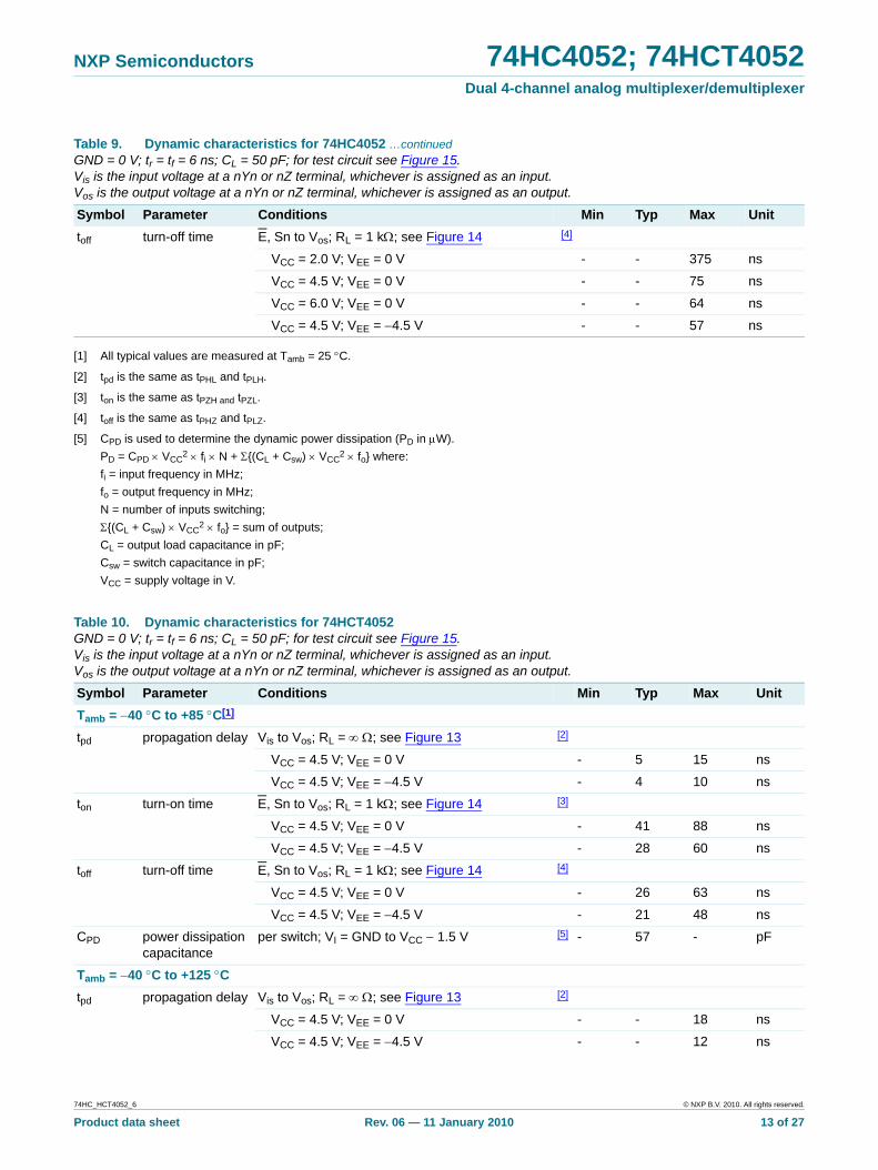
Fig 13. Input (Vis) to output (Vos) propagation delays
001aad555
tPLH tPHL
50 %
50 %Vis input
Vos output
74HC_HCT4052_6 © NXP B.V. 2010. All rights reserved.
Product data sheet Rev. 06 — 11 January 2010 14 of 27
NXP Semiconductors 74HC4052; 74HCT4052Dual 4-channel analog multiplexer/demultiplexer
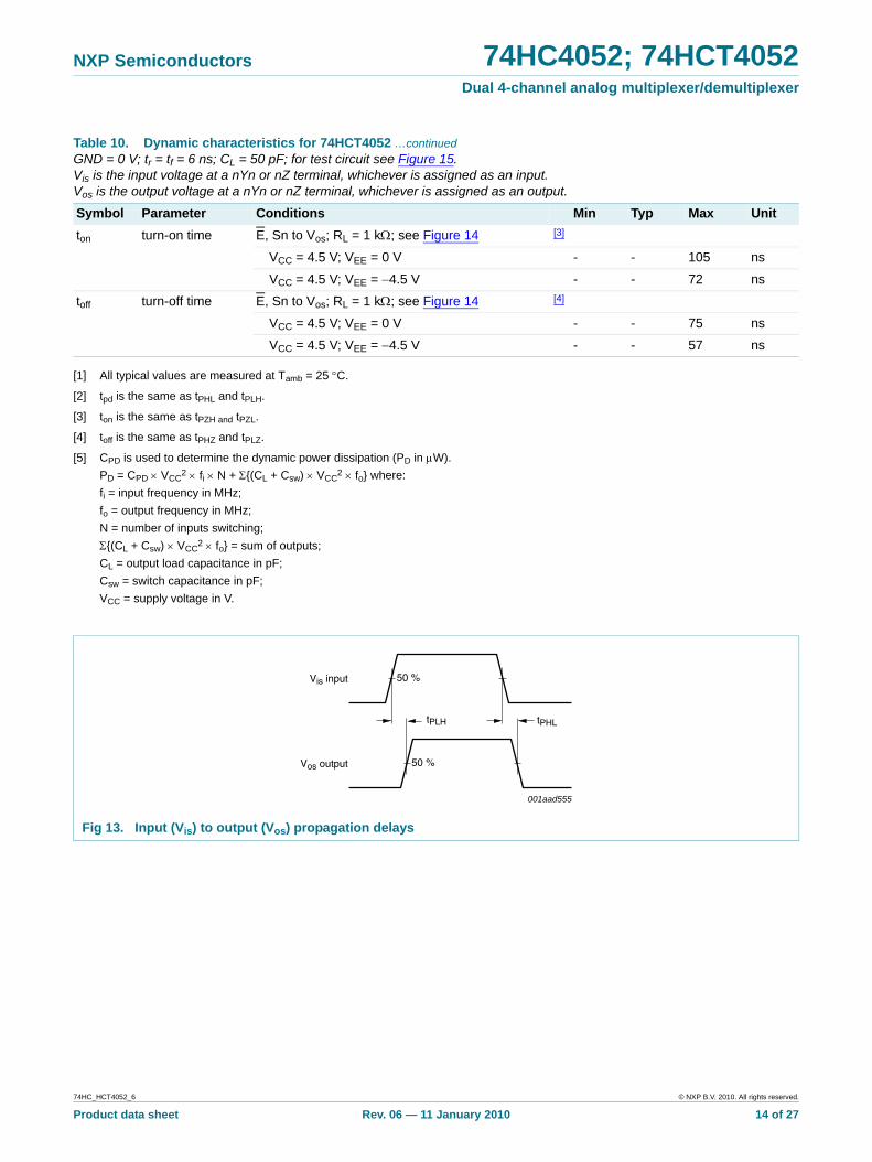
For 74HC4052: VM = 0.5 × VCC.For 74HCT4052: VM = 1.3 V.
Fig 14. Turn-on and turn-off times
001aae330
tPLZ
tPHZ
switch OFF switch ONswitch ON
Vos output
Vos output
E, Sn inputs VM
VI
0 V
90 %
10 %
tPZL
tPZH
50 %
50 %
Definitions for test circuit; see Table 11:RT = termination resistance should be equal to the output impedance Zo of the pulse generator.CL = load capacitance including jig and probe capacitance.RL = load resistance.S1 = Test selection switch.
Fig 15. Test circuit for measuring AC performance
VM VM
tW
tW
10 %
90 %
0 V
VI
VI
negativepulse
positivepulse
0 V
VM VM
90 %
10 %
tf
tr
tr
tf
001aae382
VCC VCC
open
GND
VEE
VI Vos
DUT
CLRT
RL S1PULSE
GENERATOR
Vis
74HC_HCT4052_6 © NXP B.V. 2010. All rights reserved.
Product data sheet Rev. 06 — 11 January 2010 15 of 27
NXP Semiconductors 74HC4052; 74HCT4052Dual 4-channel analog multiplexer/demultiplexer
[1] tr = tf = 6 ns; when measuring fmax, there is no constraint to tr and tf with 50 % duty factor.
[2] VI values:a) For 74HC4052: VI = VCC
b) For 74HCT4052: VI = 3 V
12. Additional dynamic characteristics
[1] Adjust input voltage Vis to 0 dBm level (0 dBm = 1 mW into 600 Ω).
[2] Adjust input voltage Vis to 0 dBm level at Vos for 1 MHz (0 dBm = 1 mW into 50 Ω).
Table 11. Test data Test Input Load S1 position
VI Vis tr, tf CL RL
at fmax other[1]
tPHL, tPLH [2] pulse < 2 ns 6 ns 50 pF 1 kΩ open
tPZH, tPHZ [2] VCC < 2 ns 6 ns 50 pF 1 kΩ VEE
tPZL, tPLZ [2] VEE < 2 ns 6 ns 50 pF 1 kΩ VCC
Table 12. Additional dynamic characteristics Recommended conditions and typical values; GND = 0 V; Tamb = 25 °C; CL = 50 pF.Vis is the input voltage at pins nYn or nZ, whichever is assigned as an input.Vos is the output voltage at pins nYn or nZ, whichever is assigned as an output.
Symbol Parameter Conditions Min Typ Max Unitdsin sine-wave distortion fi = 1 kHz; RL = 10 kΩ; see Figure 16
Vis = 4.0 V (p-p); VCC = 2.25 V; VEE = −2.25 V - 0.04 - %
Vis = 8.0 V (p-p); VCC = 4.5 V; VEE = −4.5 V - 0.02 - %
fi = 10 kHz; RL = 10 kΩ; see Figure 16
Vis = 4.0 V (p-p); VCC = 2.25 V; VEE = −2.25 V - 0.12 - %
Vis = 8.0 V (p-p); VCC = 4.5 V; VEE = −4.5 V - 0.06 - %
αiso isolation (OFF-state) RL = 600 Ω; fi = 1 MHz; see Figure 17
VCC = 2.25 V; VEE = −2.25 V [1] - −50 - dB
VCC = 4.5 V; VEE = −4.5 V [1] - −50 - dB
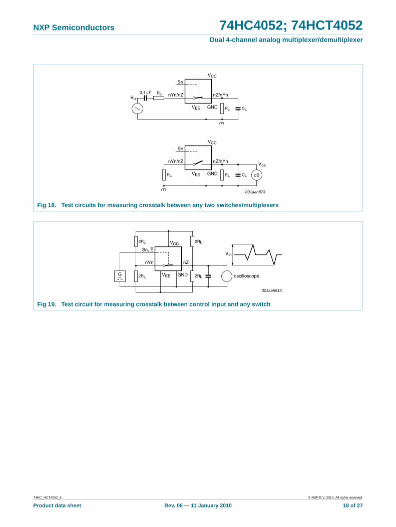
Xtalk crosstalk between two switches/multiplexers; RL = 600 Ω; fi = 1 MHz; see Figure 18
VCC = 2.25 V; VEE = −2.25 V [1] - −60 - dB
VCC = 4.5 V; VEE = −4.5 V [1] - −60 - dB
Vct crosstalk voltage peak-to-peak value; between control and any switch; RL = 600 Ω; fi = 1 MHz; E or Sn square wave between VCC and GND; tr = tf = 6 ns; see Figure 19
VCC = 4.5 V; VEE = 0 V - 110 - mV
VCC = 4.5 V; VEE = −4.5 V - 220 - mV
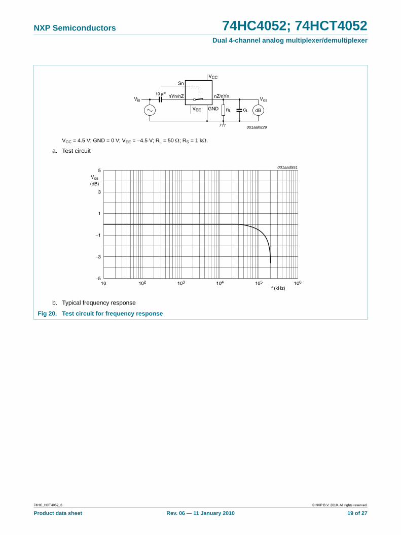
f(−3dB) −3 dB frequency response RL = 50 Ω; see Figure 20
VCC = 2.25 V; VEE = −2.25 V [2] - 170 - MHz
VCC = 4.5 V; VEE = −4.5 V [2] - 180 - MHz
74HC_HCT4052_6 © NXP B.V. 2010. All rights reserved.
Product data sheet Rev. 06 — 11 January 2010 16 of 27
NXP Semiconductors 74HC4052; 74HCT4052Dual 4-channel analog multiplexer/demultiplexer
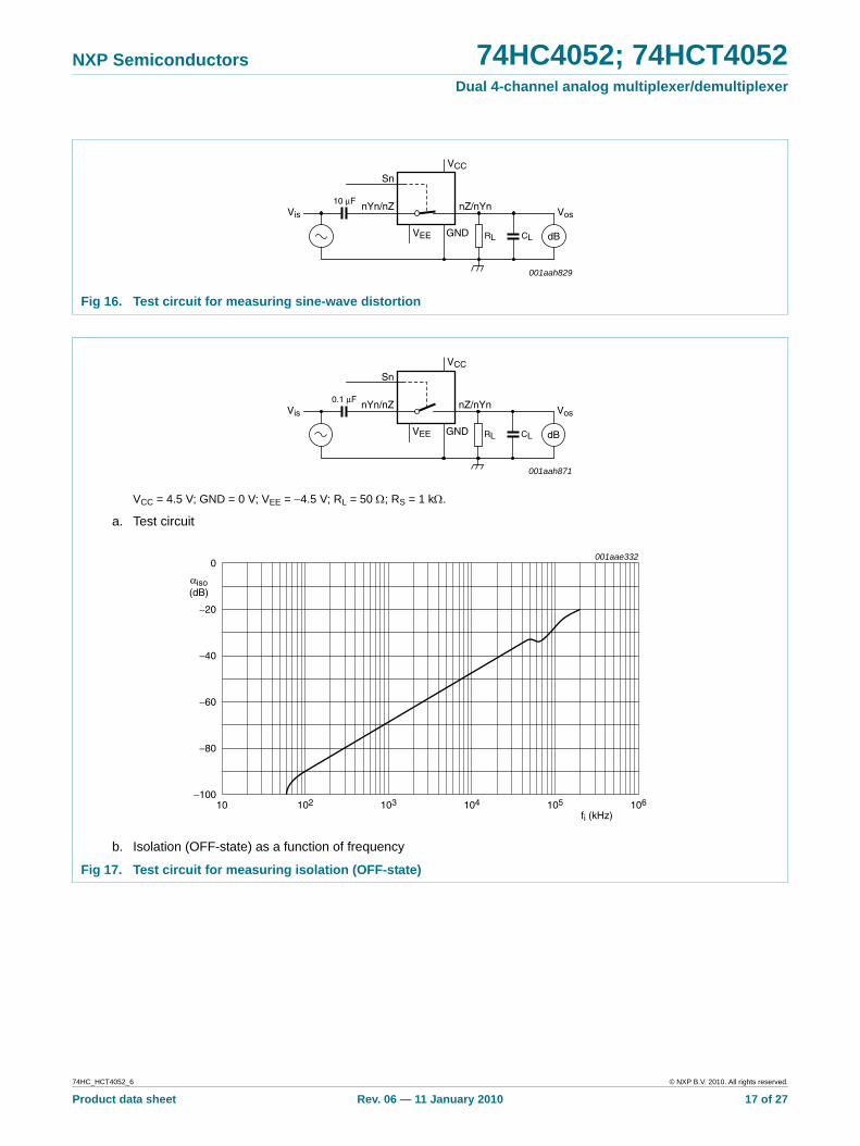
Fig 16. Test circuit for measuring sine-wave distortion
dB
001aah829
nYn/nZ10 μFVis Vos
nZ/nYn
CLRL
Sn
GNDVEE
VCC
VCC = 4.5 V; GND = 0 V; VEE = −4.5 V; RL = 50 Ω; RS = 1 kΩ.
a. Test circuit
b. Isolation (OFF-state) as a function of frequency
Fig 17. Test circuit for measuring isolation (OFF-state)
dB
001aah871
nYn/nZ0.1 μFVis Vos
nZ/nYn
CLRL
Sn
GNDVEE
VCC
001aae332
fi (kHz)10 105 106104102 103
−60
−40
−80
−20
0
αiso(dB)
−100
74HC_HCT4052_6 © NXP B.V. 2010. All rights reserved.
Product data sheet Rev. 06 — 11 January 2010 17 of 27
NXP Semiconductors 74HC4052; 74HCT4052Dual 4-channel analog multiplexer/demultiplexer
Fig 18. Test circuits for measuring crosstalk between any two switches/multiplexers
dB
001aah873
nYn/nZ VosnZ/nYn
CLRLRL
Sn
GNDVEE
VCC
nYn/nZ0.1 μFVis
nZ/nYn
CLRL
RL
Sn
GNDVEE
VCC
Fig 19. Test circuit for measuring crosstalk between control input and any switch
oscilloscope
001aah913
nYn
Vct
nZ
2RL 2RL
2RL 2RL
Sn, E
GNDVEE
VCC
G
74HC_HCT4052_6 © NXP B.V. 2010. All rights reserved.
Product data sheet Rev. 06 — 11 January 2010 18 of 27
NXP Semiconductors 74HC4052; 74HCT4052Dual 4-channel analog multiplexer/demultiplexer
VCC = 4.5 V; GND = 0 V; VEE = −4.5 V; RL = 50 Ω; RS = 1 kΩ.
a. Test circuit
b. Typical frequency response
Fig 20. Test circuit for frequency response
dB
001aah829
nYn/nZ10 μFVis Vos
nZ/nYn
CLRL
Sn
GNDVEE
VCC
001aad551
f (kHz)10 105 106104102 103
−1
1
−3
3
5Vos(dB)
−5
74HC_HCT4052_6 © NXP B.V. 2010. All rights reserved.
Product data sheet Rev. 06 — 11 January 2010 19 of 27
NXP Semiconductors 74HC4052; 74HCT4052Dual 4-channel analog multiplexer/demultiplexer
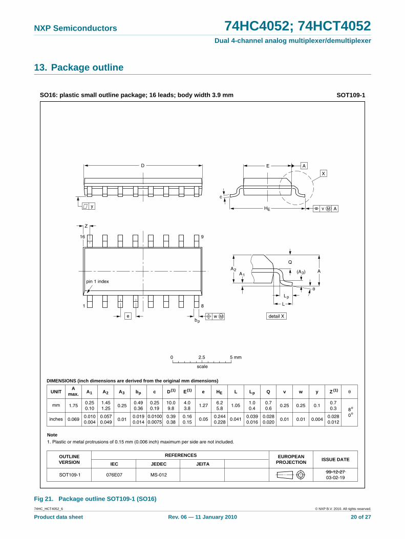
13. Package outline
Fig 21. Package outline SOT109-1 (SO16)
X
w M
θ
AA1
A2
bp
D
HE
Lp
Q
detail X
E
Z
e
c
L
v M A
(A )3
A
8
9
1
16
y
pin 1 index
UNITA
max. A1 A2 A3 bp c D(1) E(1) (1)e HE L Lp Q Zywv θ
REFERENCESOUTLINEVERSION
EUROPEANPROJECTION ISSUE DATE
IEC JEDEC JEITA
mm
inches
1.750.250.10
1.451.25
0.250.490.36
0.250.19
10.09.8
4.03.8
1.276.25.8
0.70.6
0.70.3 8
0
o
o
0.25 0.1
DIMENSIONS (inch dimensions are derived from the original mm dimensions)
Note
1. Plastic or metal protrusions of 0.15 mm (0.006 inch) maximum per side are not included.
1.00.4
SOT109-199-12-2703-02-19
076E07 MS-012
0.0690.0100.004
0.0570.049
0.010.0190.014
0.01000.0075
0.390.38
0.160.15
0.05
1.05
0.0410.2440.228
0.0280.020
0.0280.012
0.01
0.25
0.01 0.0040.0390.016
0 2.5 5 mm
scale
SO16: plastic small outline package; 16 leads; body width 3.9 mm SOT109-1
74HC_HCT4052_6 © NXP B.V. 2010. All rights reserved.
Product data sheet Rev. 06 — 11 January 2010 20 of 27
NXP Semiconductors 74HC4052; 74HCT4052Dual 4-channel analog multiplexer/demultiplexer
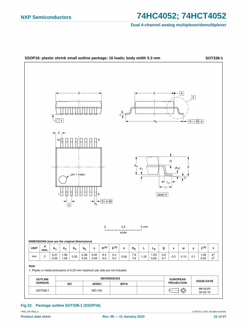
Fig 22. Package outline SOT338-1 (SSOP16)
UNIT A1 A2 A3 bp c D(1) E (1) e HE L Lp Q Zywv θ
REFERENCESOUTLINEVERSION
EUROPEANPROJECTION ISSUE DATE
IEC JEDEC JEITA
mm 0.210.05
1.801.65
0.250.380.25
0.200.09
6.46.0
5.45.2
0.65 1.257.97.6
1.030.63
0.90.7
1.000.55
80
o
o0.130.2 0.1
DIMENSIONS (mm are the original dimensions)
Note
1. Plastic or metal protrusions of 0.25 mm maximum per side are not included.
SOT338-199-12-2703-02-19
(1)
w Mbp
D
HE
E
Z
e
c
v M A
XA
y
1 8
16 9
θ
AA1
A2
Lp
Q
detail X
L
(A )3
MO-150
pin 1 index
0 2.5 5 mm
scale
SSOP16: plastic shrink small outline package; 16 leads; body width 5.3 mm SOT338-1
Amax.
2
74HC_HCT4052_6 © NXP B.V. 2010. All rights reserved.
Product data sheet Rev. 06 — 11 January 2010 21 of 27
NXP Semiconductors 74HC4052; 74HCT4052Dual 4-channel analog multiplexer/demultiplexer
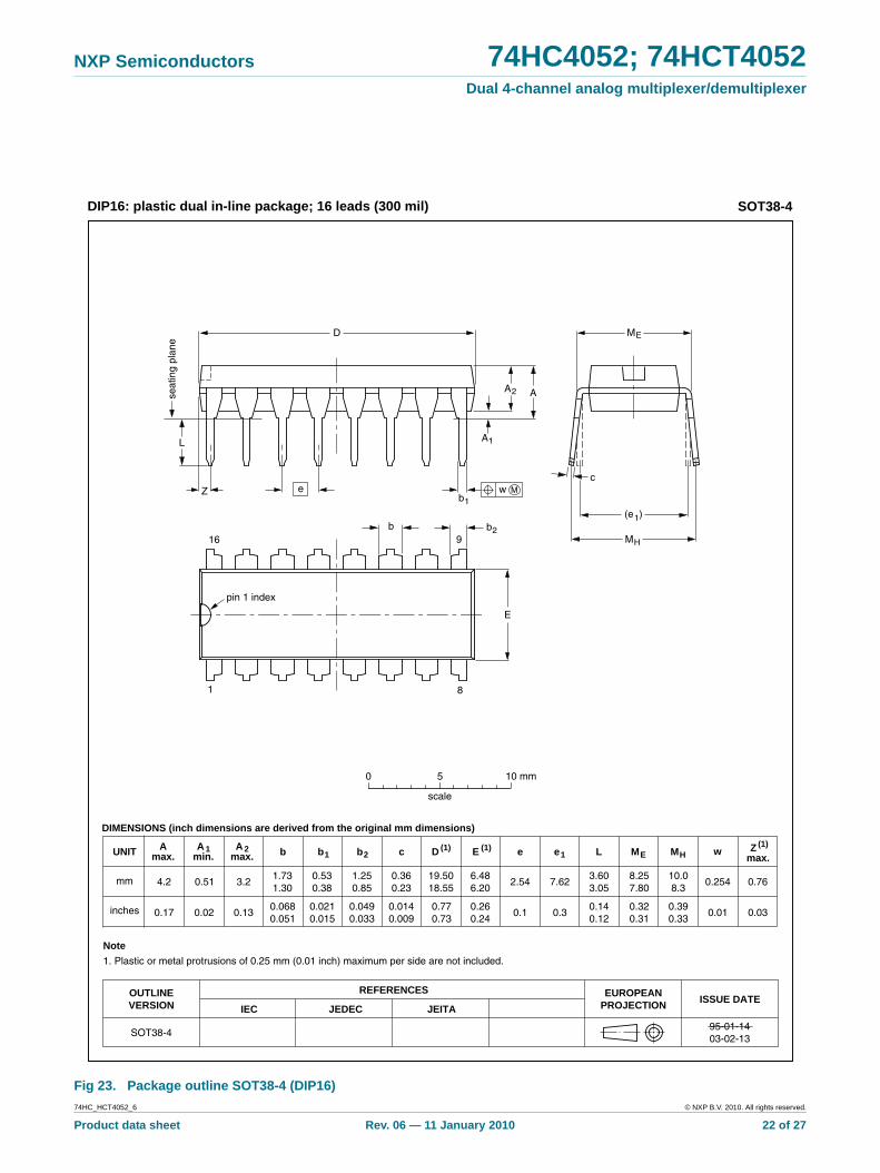
Fig 23. Package outline SOT38-4 (DIP16)
REFERENCESOUTLINEVERSION
EUROPEANPROJECTION ISSUE DATE
IEC JEDEC JEITA
SOT38-495-01-1403-02-13
MH
c
(e )1
ME
A
L
seat
ing
plan
e
A1
w Mb1
b2
e
D
A2
Z
16
1
9
8
E
pin 1 index
b
0 5 10 mm
scale
Note
1. Plastic or metal protrusions of 0.25 mm (0.01 inch) maximum per side are not included.
UNIT Amax.
1 2 b1(1) (1) (1)
b2 c D E e M ZHL
mm
DIMENSIONS (inch dimensions are derived from the original mm dimensions)
A min.
A max. b
max.wMEe1
1.731.30
0.530.38
0.360.23
19.5018.55
6.486.20
3.603.05
0.2542.54 7.628.257.80
10.08.3
0.764.2 0.51 3.2
inches 0.0680.051
0.0210.015
0.0140.009
1.250.85
0.0490.033
0.770.73
0.260.24
0.140.12
0.010.1 0.30.320.31
0.390.33
0.030.17 0.02 0.13
DIP16: plastic dual in-line package; 16 leads (300 mil) SOT38-4
74HC_HCT4052_6 © NXP B.V. 2010. All rights reserved.
Product data sheet Rev. 06 — 11 January 2010 22 of 27
NXP Semiconductors 74HC4052; 74HCT4052Dual 4-channel analog multiplexer/demultiplexer
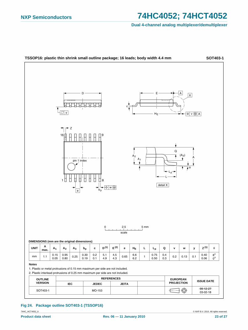
Fig 24. Package outline SOT403-1 (TSSOP16)
UNIT A1 A2 A3 bp c D (1) E (2) (1)e HE L Lp Q Zywv θ
REFERENCESOUTLINEVERSION
EUROPEANPROJECTION ISSUE DATE
IEC JEDEC JEITA
mm 0.150.05
0.950.80
0.300.19
0.20.1
5.14.9
4.54.3
0.656.66.2
0.40.3
0.400.06
80
o
o0.13 0.10.21
DIMENSIONS (mm are the original dimensions)
Notes
1. Plastic or metal protrusions of 0.15 mm maximum per side are not included.
2. Plastic interlead protrusions of 0.25 mm maximum per side are not included.
0.750.50
SOT403-1 MO-15399-12-2703-02-18
w Mbp
D
Z
e
0.25
1 8
16 9
θ
AA1
A2
Lp
Q
detail X
L
(A )3
HE
E
c
v M A
XA
y
0 2.5 5 mm
scale
TSSOP16: plastic thin shrink small outline package; 16 leads; body width 4.4 mm SOT403-1
Amax.
1.1
pin 1 index
74HC_HCT4052_6 © NXP B.V. 2010. All rights reserved.
Product data sheet Rev. 06 — 11 January 2010 23 of 27
NXP Semiconductors 74HC4052; 74HCT4052Dual 4-channel analog multiplexer/demultiplexer
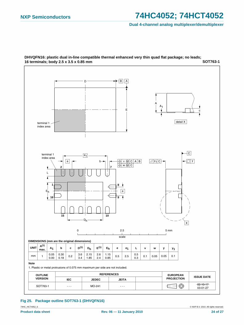
Fig 25. Package outline SOT763-1 (DHVQFN16)
terminal 1index area
0.51
A1 EhbUNIT ye
0.2
c
REFERENCESOUTLINEVERSION
EUROPEANPROJECTION ISSUE DATE
IEC JEDEC JEITA
mm 3.63.4
Dh
2.151.85
y1
2.62.4
1.150.85
e1
2.50.300.18
0.050.00
0.05 0.1
DIMENSIONS (mm are the original dimensions)
SOT763-1 MO-241 - - -- - -
0.50.3
L
0.1
v
0.05
w
0 2.5 5 mm
scale
SOT763-1DHVQFN16: plastic dual in-line compatible thermal enhanced very thin quad flat package; no leads;16 terminals; body 2.5 x 3.5 x 0.85 mm
A(1)
max.
AA1
c
detail X
yy1 Ce
L
Eh
Dh
e
e1
b
2 7
15 10
9
81
16
X
D
E
C
B A
terminal 1index area
ACC
Bv M
w M
E(1)
Note
1. Plastic or metal protrusions of 0.075 mm maximum per side are not included.
D(1)
02-10-1703-01-27
74HC_HCT4052_6 © NXP B.V. 2010. All rights reserved.
Product data sheet Rev. 06 — 11 January 2010 24 of 27
NXP Semiconductors 74HC4052; 74HCT4052Dual 4-channel analog multiplexer/demultiplexer
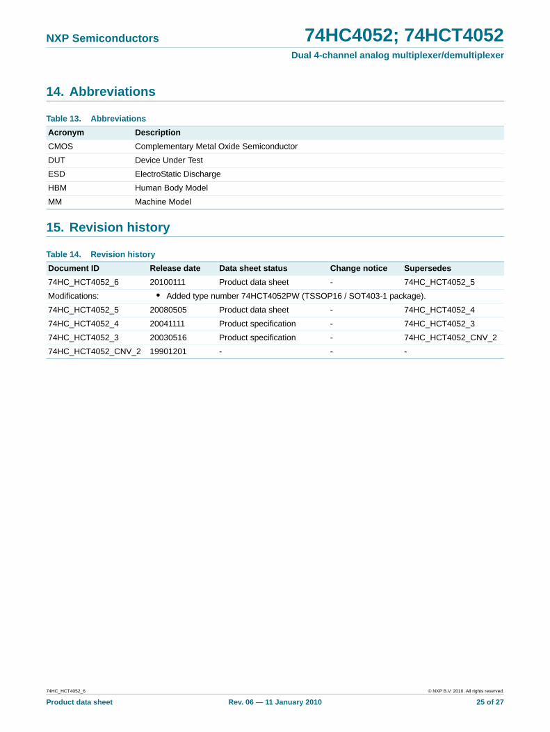
14. Abbreviations
15. Revision history
Table 13. Abbreviations Acronym DescriptionCMOS Complementary Metal Oxide Semiconductor
DUT Device Under Test
ESD ElectroStatic Discharge
HBM Human Body Model
MM Machine Model
Table 14. Revision history Document ID Release date Data sheet status Change notice Supersedes74HC_HCT4052_6 20100111 Product data sheet - 74HC_HCT4052_5
Modifications: • Added type number 74HCT4052PW (TSSOP16 / SOT403-1 package).
74HC_HCT4052_5 20080505 Product data sheet - 74HC_HCT4052_4
74HC_HCT4052_4 20041111 Product specification - 74HC_HCT4052_3
74HC_HCT4052_3 20030516 Product specification - 74HC_HCT4052_CNV_2
74HC_HCT4052_CNV_2 19901201 - - -
74HC_HCT4052_6 © NXP B.V. 2010. All rights reserved.
Product data sheet Rev. 06 — 11 January 2010 25 of 27
NXP Semiconductors 74HC4052; 74HCT4052Dual 4-channel analog multiplexer/demultiplexer
16. Legal information
16.1 Data sheet status
[1] Please consult the most recently issued document before initiating or completing a design.
[2] The term ‘short data sheet’ is explained in section “Definitions”.
[3] The product status of device(s) described in this document may have changed since this document was published and may differ in case of multiple devices. The latest product status information is available on the Internet at URL http://www.nxp.com.
16.2 DefinitionsDraft — The document is a draft version only. The content is still under internal review and subject to formal approval, which may result in modifications or additions. NXP Semiconductors does not give any representations or warranties as to the accuracy or completeness of information included herein and shall have no liability for the consequences of use of such information.
Short data sheet — A short data sheet is an extract from a full data sheet with the same product type number(s) and title. A short data sheet is intended for quick reference only and should not be relied upon to contain detailed and full information. For detailed and full information see the relevant full data sheet, which is available on request via the local NXP Semiconductors sales office. In case of any inconsistency or conflict with the short data sheet, the full data sheet shall prevail.
16.3 DisclaimersGeneral — Information in this document is believed to be accurate and reliable. However, NXP Semiconductors does not give any representations or warranties, expressed or implied, as to the accuracy or completeness of such information and shall have no liability for the consequences of use of such information.
Right to make changes — NXP Semiconductors reserves the right to make changes to information published in this document, including without limitation specifications and product descriptions, at any time and without notice. This document supersedes and replaces all information supplied prior to the publication hereof.
Suitability for use — NXP Semiconductors products are not designed, authorized or warranted to be suitable for use in medical, military, aircraft, space or life support equipment, nor in applications where failure or malfunction of an NXP Semiconductors product can reasonably be expected to result in personal injury, death or severe property or environmental
damage. NXP Semiconductors accepts no liability for inclusion and/or use of NXP Semiconductors products in such equipment or applications and therefore such inclusion and/or use is at the customer’s own risk.
Applications — Applications that are described herein for any of these products are for illustrative purposes only. NXP Semiconductors makes no representation or warranty that such applications will be suitable for the specified use without further testing or modification.
Limiting values — Stress above one or more limiting values (as defined in the Absolute Maximum Ratings System of IEC 60134) may cause permanent damage to the device. Limiting values are stress ratings only and operation of the device at these or any other conditions above those given in the Characteristics sections of this document is not implied. Exposure to limiting values for extended periods may affect device reliability.
Terms and conditions of sale — NXP Semiconductors products are sold subject to the general terms and conditions of commercial sale, as published at http://www.nxp.com/profile/terms, including those pertaining to warranty, intellectual property rights infringement and limitation of liability, unless explicitly otherwise agreed to in writing by NXP Semiconductors. In case of any inconsistency or conflict between information in this document and such terms and conditions, the latter will prevail.
No offer to sell or license — Nothing in this document may be interpreted or construed as an offer to sell products that is open for acceptance or the grant, conveyance or implication of any license under any copyrights, patents or other industrial or intellectual property rights.
Export control — This document as well as the item(s) described herein may be subject to export control regulations. Export might require a prior authorization from national authorities.
16.4 TrademarksNotice: All referenced brands, product names, service names and trademarks are the property of their respective owners.
17. Contact information
For more information, please visit: http://www.nxp.com
For sales office addresses, please send an email to: [email protected]
Document status[1][2] Product status[3] Definition
Objective [short] data sheet Development This document contains data from the objective specification for product development.
Preliminary [short] data sheet Qualification This document contains data from the preliminary specification.
Product [short] data sheet Production This document contains the product specification.
74HC_HCT4052_6 © NXP B.V. 2010. All rights reserved.
Product data sheet Rev. 06 — 11 January 2010 26 of 27
NXP Semiconductors 74HC4052; 74HCT4052Dual 4-channel analog multiplexer/demultiplexer
18. Contents
1 General description . . . . . . . . . . . . . . . . . . . . . . 12 Features . . . . . . . . . . . . . . . . . . . . . . . . . . . . . . . 13 Applications . . . . . . . . . . . . . . . . . . . . . . . . . . . . 14 Ordering information. . . . . . . . . . . . . . . . . . . . . 25 Functional diagram . . . . . . . . . . . . . . . . . . . . . . 26 Pinning information. . . . . . . . . . . . . . . . . . . . . . 46.1 Pinning . . . . . . . . . . . . . . . . . . . . . . . . . . . . . . . 46.2 Pin description . . . . . . . . . . . . . . . . . . . . . . . . . 47 Functional description . . . . . . . . . . . . . . . . . . . 57.1 Function table . . . . . . . . . . . . . . . . . . . . . . . . . . 58 Limiting values. . . . . . . . . . . . . . . . . . . . . . . . . . 59 Recommended operating conditions. . . . . . . . 610 Static characteristics. . . . . . . . . . . . . . . . . . . . . 711 Dynamic characteristics . . . . . . . . . . . . . . . . . 1212 Additional dynamic characteristics . . . . . . . . 1613 Package outline . . . . . . . . . . . . . . . . . . . . . . . . 2014 Abbreviations. . . . . . . . . . . . . . . . . . . . . . . . . . 2515 Revision history. . . . . . . . . . . . . . . . . . . . . . . . 2516 Legal information. . . . . . . . . . . . . . . . . . . . . . . 2616.1 Data sheet status . . . . . . . . . . . . . . . . . . . . . . 2616.2 Definitions. . . . . . . . . . . . . . . . . . . . . . . . . . . . 2616.3 Disclaimers . . . . . . . . . . . . . . . . . . . . . . . . . . . 2616.4 Trademarks. . . . . . . . . . . . . . . . . . . . . . . . . . . 2617 Contact information. . . . . . . . . . . . . . . . . . . . . 2618 Contents . . . . . . . . . . . . . . . . . . . . . . . . . . . . . . 27
© NXP B.V. 2010. All rights reserved.For more information, please visit: http://www.nxp.com For sales office addresses, please send an email to: [email protected]
Date of release: 11 January 2010Document identifier: 74HC_HCT4052_6
Please be aware that important notices concerning this document and the product(s) described herein, have been included in section ‘Legal information’.