Embed Size (px)
Citation preview
Chapter 5Synchronous Sequential Logic
• Sequential Circuits• Latches and FlipFlops• Analysis of Clocked Sequential Circuits• HDL• Optimization• Design Procedure
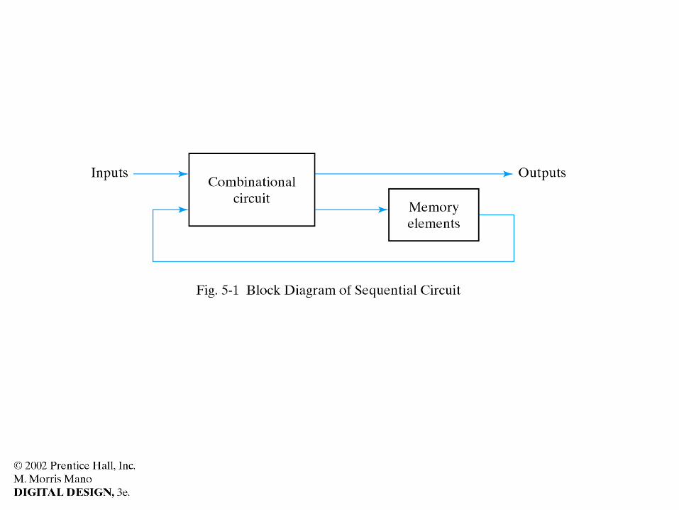
Sequential Circuits
• Various definitions– Combinational circuits with feedback– Combinational circuits with memory– Combinational circuits with state– whatever...
Synchronous...
• If there are synchronous circuits, there must be asynchronous as well.
• We (and everybody else) deal mostly with synchronous.
• Synchronous circuits have a clock (it can take a few different forms)
Asynchronous circuits
• Depend on time delay devices for storage• Can exhibit instabilities (due to effects like
racing conditions)• Hard to design• Used mainly for special subcomponents
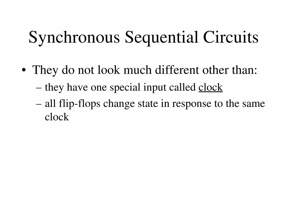
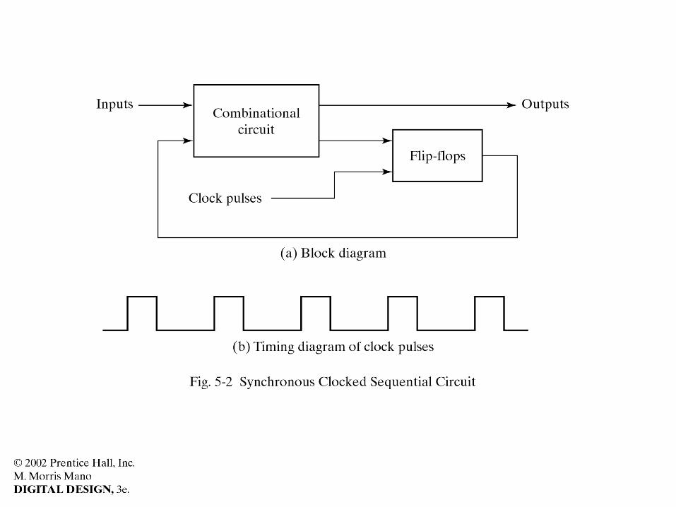
Synchronous Sequential Circuits
• They do not look much different other than:– they have one special input called clock– all flipflops change state in response to the same
clock
Latches
• The simplest kind of memory• They are primitive flipflops• Flipflops can contain one or more latches
– usually more
• Great for understanding flipflops without having to know electronics
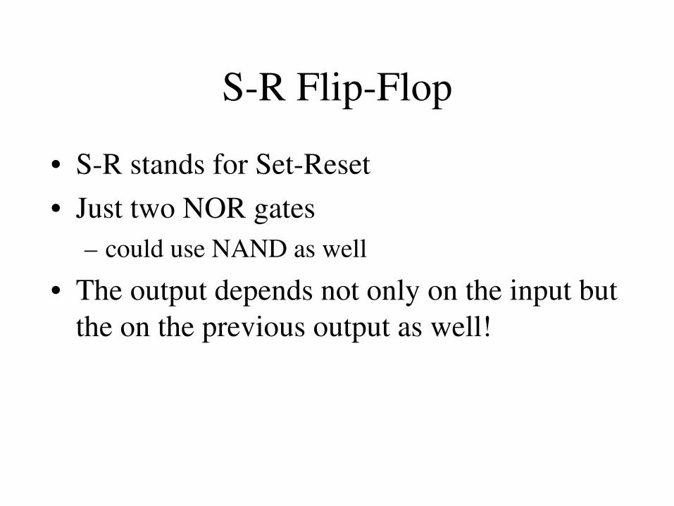
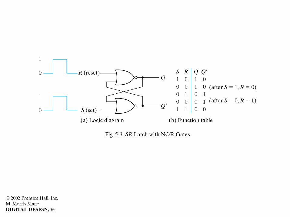
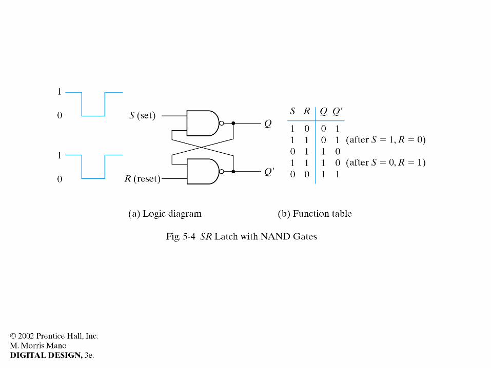
SR FlipFlop
• SR stands for SetReset• Just two NOR gates
– could use NAND as well
• The output depends not only on the input but the on the previous output as well!
Using NAND
• Everything is just the opposite• Set and Reset are active low• The illegal input is 00
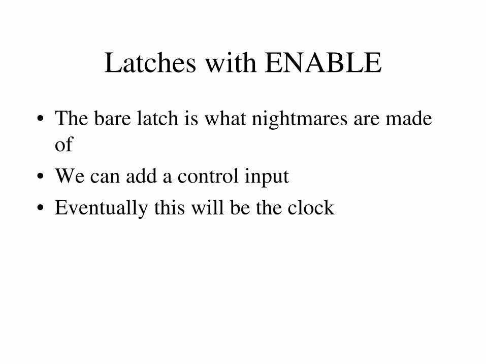
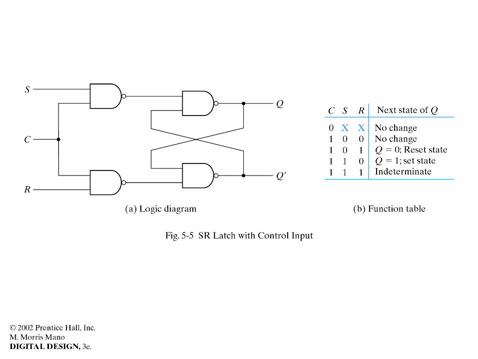
Latches with ENABLE
• The bare latch is what nightmares are made of
• We can add a control input• Eventually this will be the clock
Is it perfect?
• It has an indeterminate next state• What if the feedback propagates more than
once– This could lead to more indeterminacies– It would require a very short clock pulse.
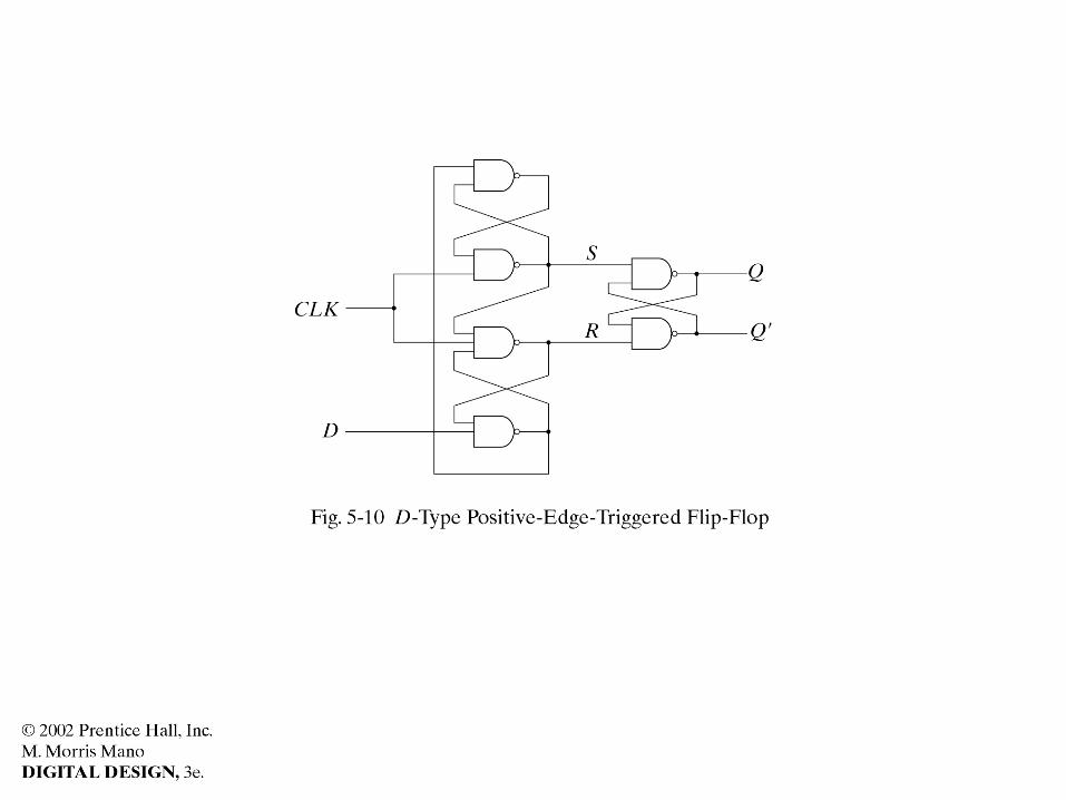
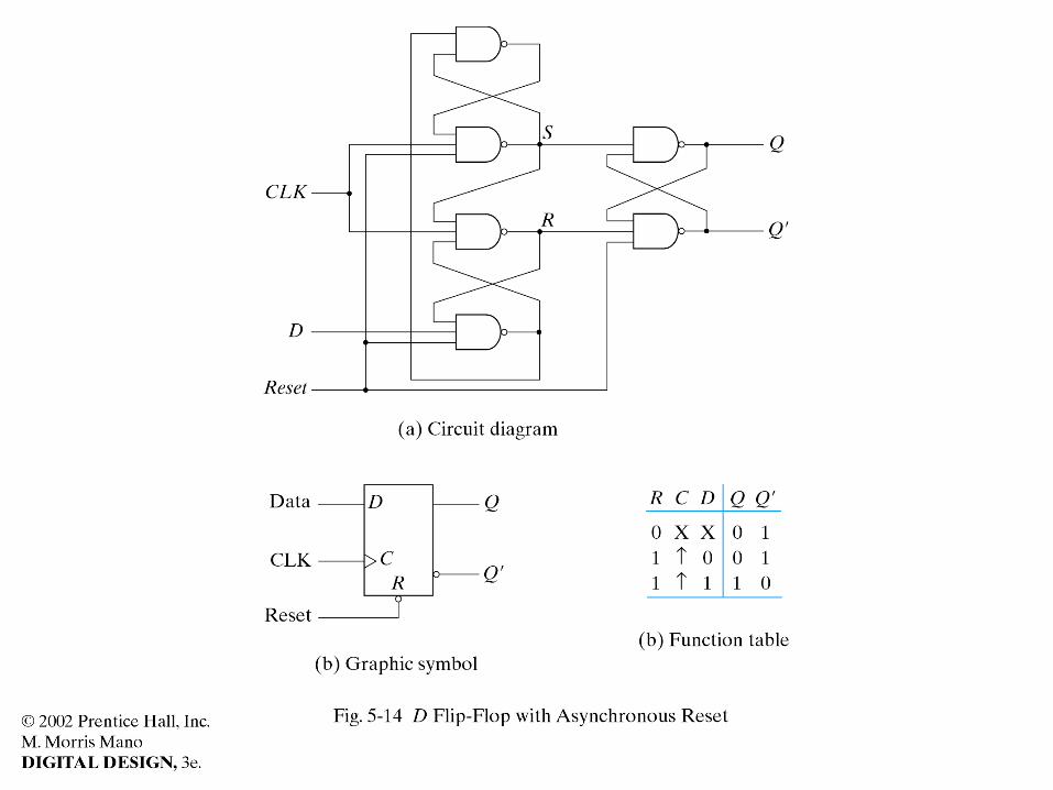
D FlipFlop
• The D flipflop has one input• The D stands for Data or Delay• With one input it is hard to have an illegal
input
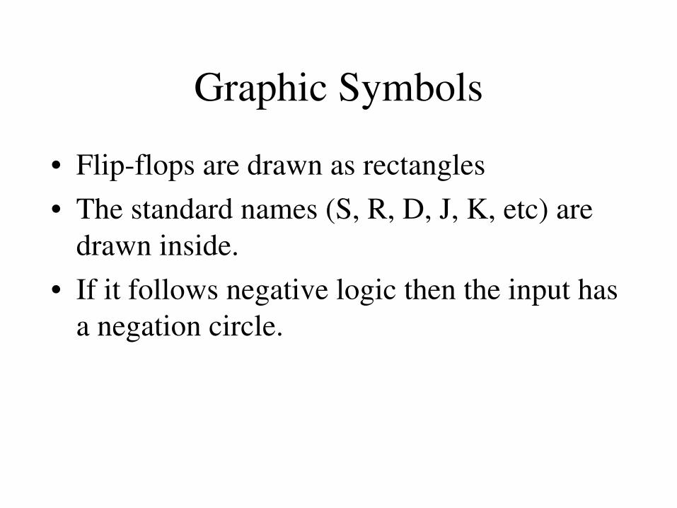
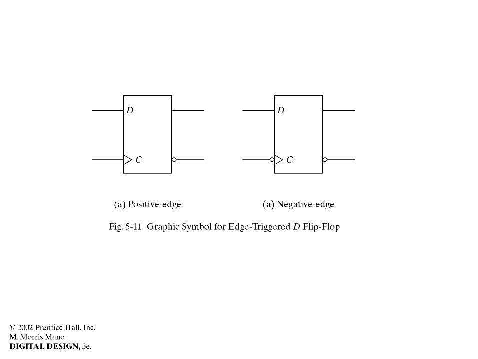
Graphic Symbols
• Flipflops are drawn as rectangles• The standard names (S, R, D, J, K, etc) are
drawn inside.• If it follows negative logic then the input has
a negation circle.
Edge Triggered FlipFlops
• A long clock pulse can create problems• This is because the flipflop is triggered by
the “level” of the clock pulse• How about if it is triggered by the transition
of the clock pulse• Such flipflops are edge triggered
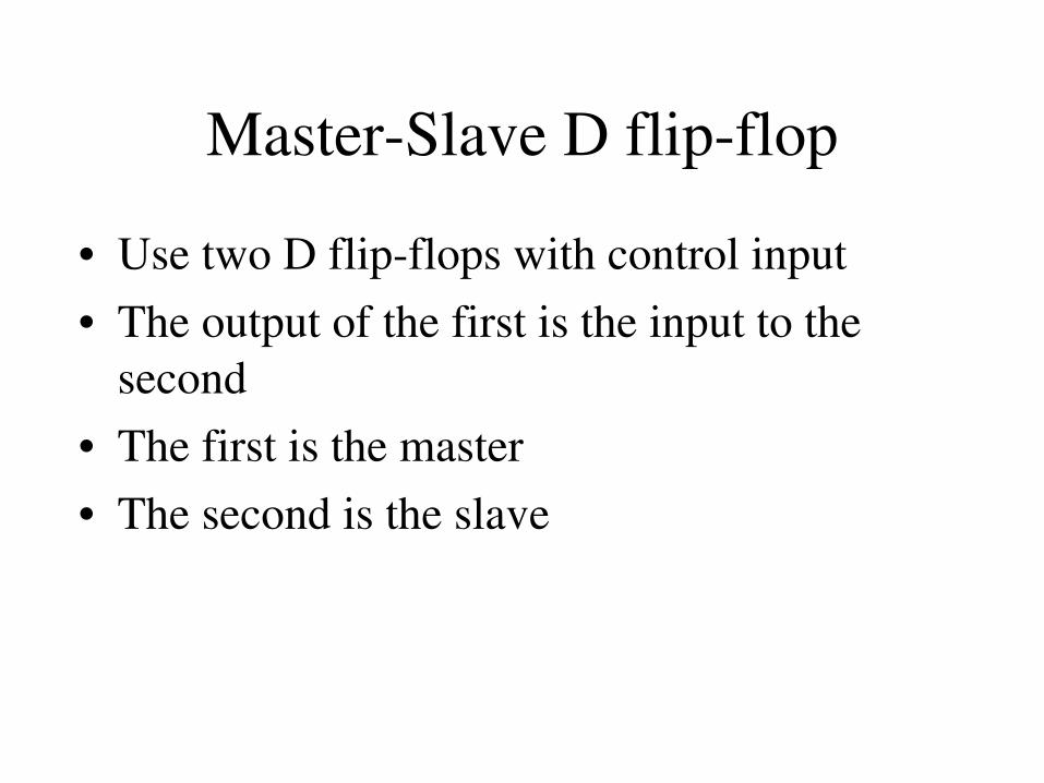
MasterSlave D flipflop
• Use two D flipflops with control input• The output of the first is the input to the
second• The first is the master• The second is the slave
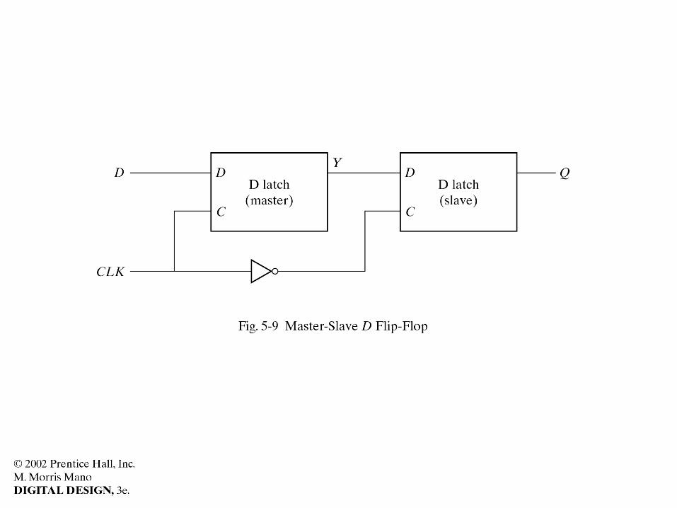
MasterSlave Operation
• When the CLK is low the slave copies the state of the master
• When the clock is high the state of the master is copied from its input
• The input cannot propagate more than one stage per clock transition.
MasterSlave Alternatives
• MasterSlave is not the only known solution.• A less expensive version would need three
bare latches
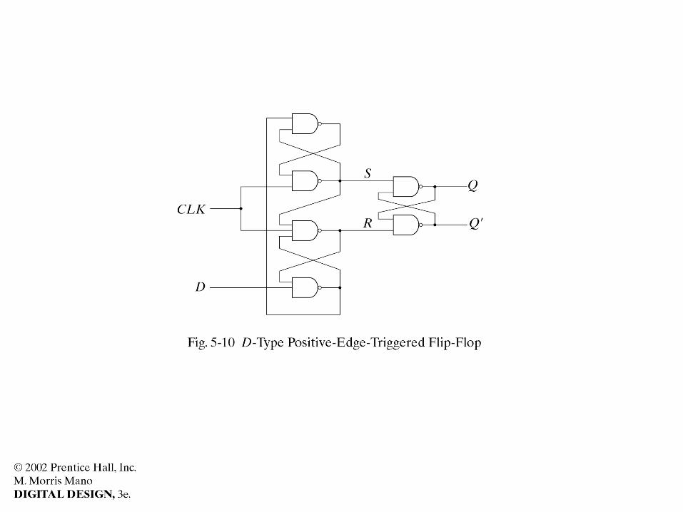
Operation
• When the CLK is 0 the input to the SR output latch is 11, and the output is maintained.
• When the CLK goes 1, the S of the output latch becomes equal to D and R becomes equal to D’
• If D changes while CLK is high, the SR are not affected
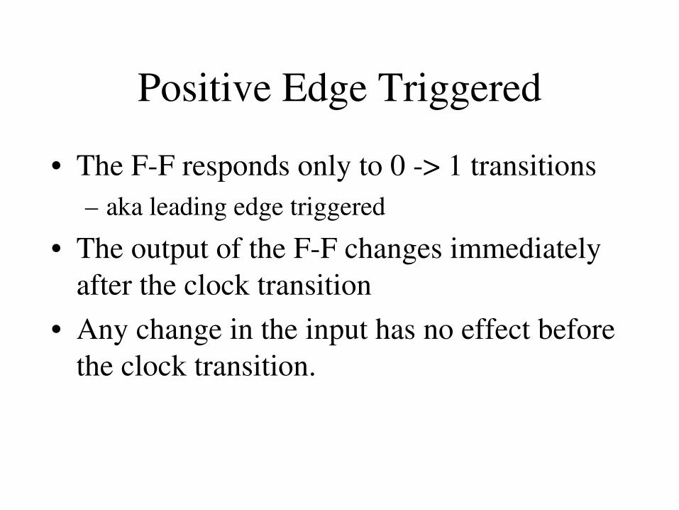
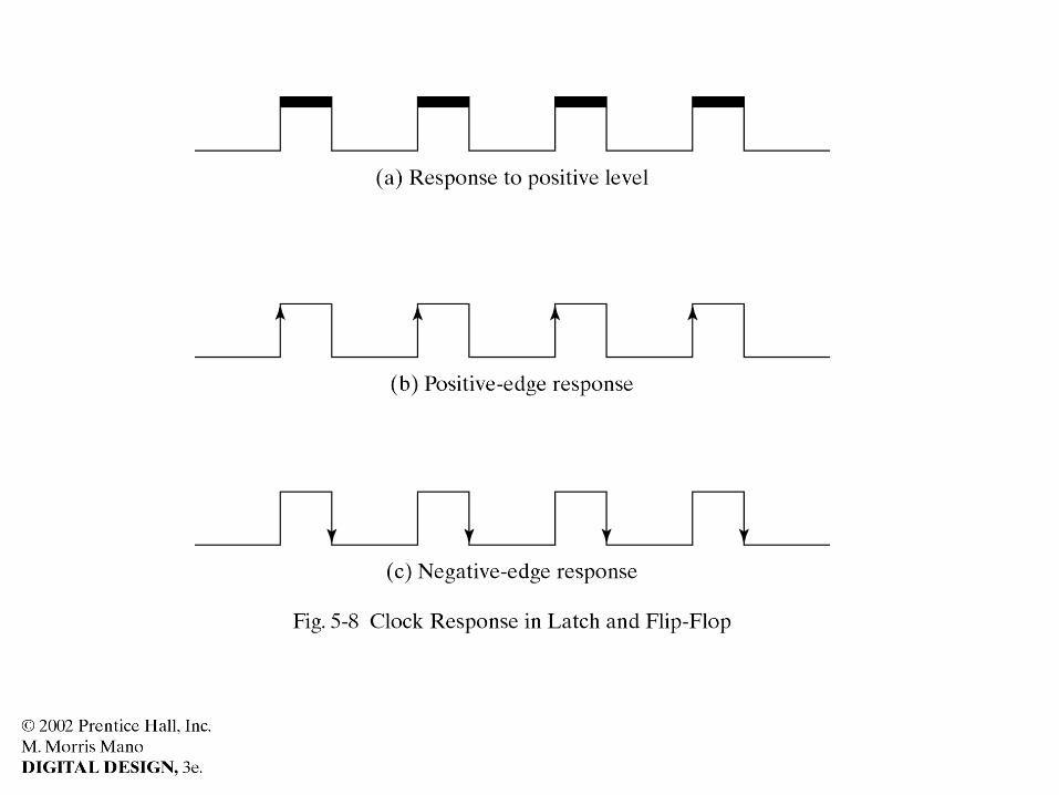
Positive Edge Triggered
• The FF responds only to 0 > 1 transitions– aka leading edge triggered
• The output of the FF changes immediately after the clock transition
• Any change in the input has no effect before the clock transition.
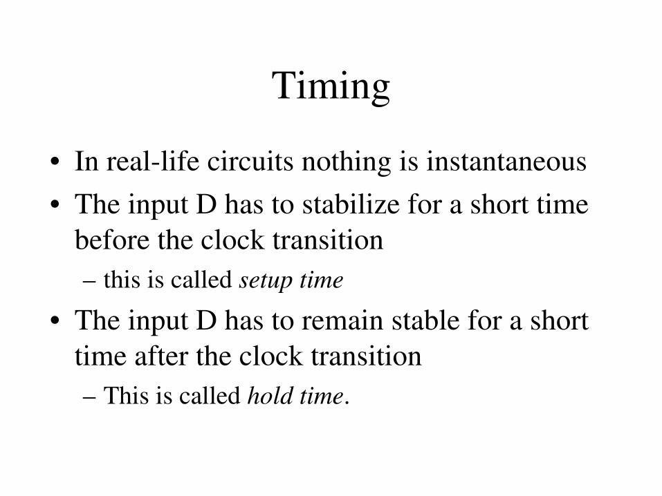
Timing
• In reallife circuits nothing is instantaneous• The input D has to stabilize for a short time
before the clock transition– this is called setup time
• The input D has to remain stable for a short time after the clock transition– This is called hold time.
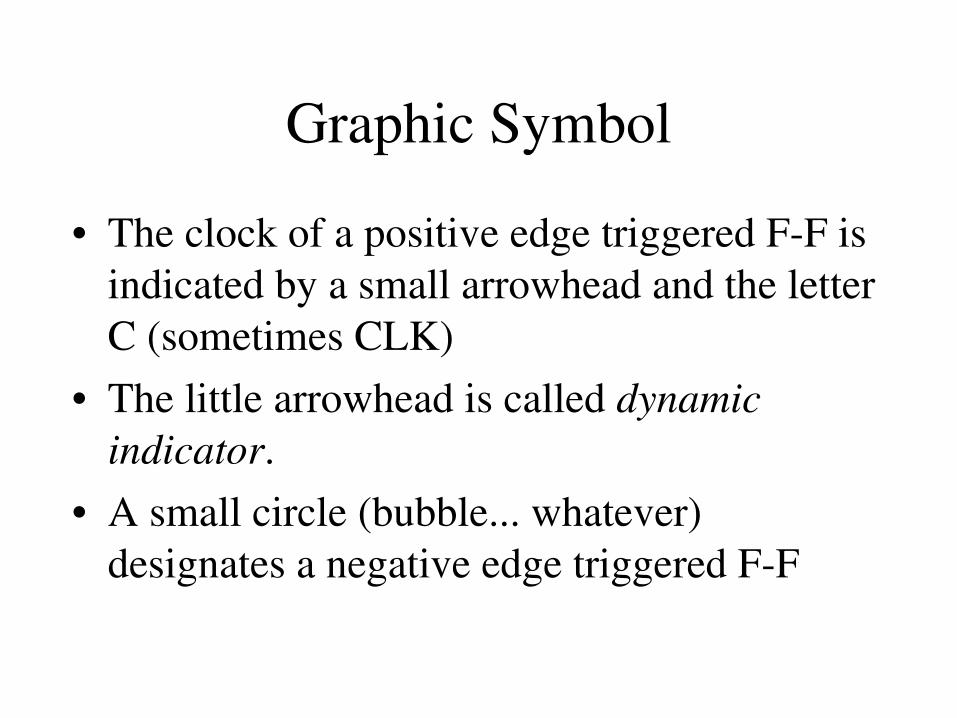
Graphic Symbol
• The clock of a positive edge triggered FF is indicated by a small arrowhead and the letter C (sometimes CLK)
• The little arrowhead is called dynamic indicator.
• A small circle (bubble... whatever) designates a negative edge triggered FF
Other FlipFlops
• The least expensive FF is the edge triggered D FF (if you count VLSI real estate)
• It needs the fewest gates to implement.• Often it needs the smallest total number of
gates (gates inside the FF and external logic)
Other FlipFlops
• Other FFs can be built using D FFs• There are three desired operations on a FF
– Set (to 1)– Reset (to 0)– Toggle
JK FlipFlop
• Can do all desired operations• Usually needs the smallest number of
external gates (its excitation table has many don’t cares)
• Often the best when using MSI technologies• Less impressive in VLSI implementations• Like SR but without illegal inputs
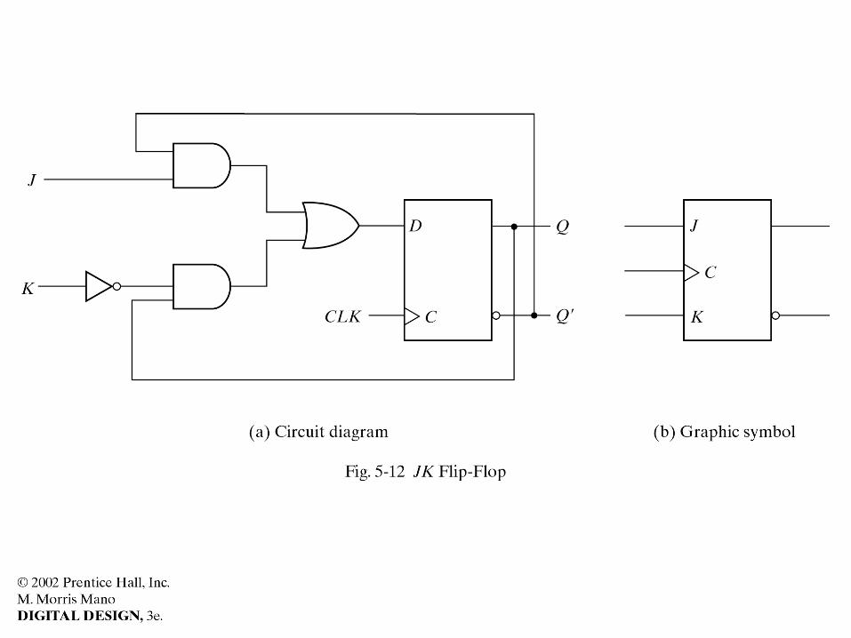
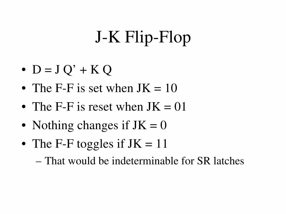
JK FlipFlop
• D = J Q’ + K Q• The FF is set when JK = 10• The FF is reset when JK = 01• Nothing changes if JK = 0• The FF toggles if JK = 11
– That would be indeterminable for SR latches
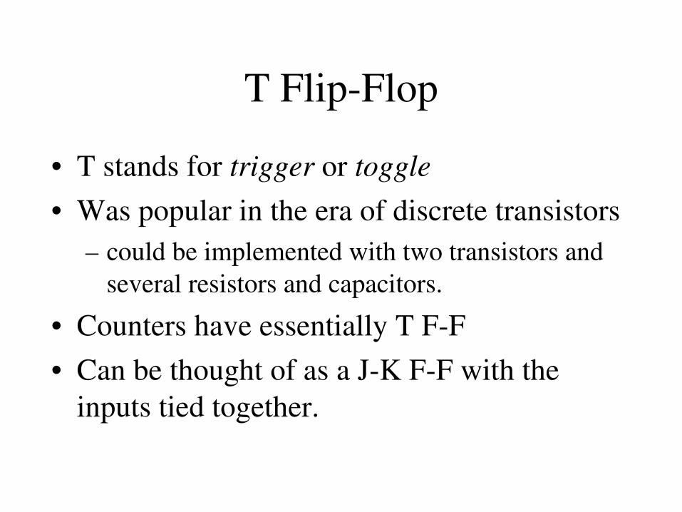
T FlipFlop
• T stands for trigger or toggle• Was popular in the era of discrete transistors
– could be implemented with two transistors and several resistors and capacitors.
• Counters have essentially T FF• Can be thought of as a JK FF with the
inputs tied together.
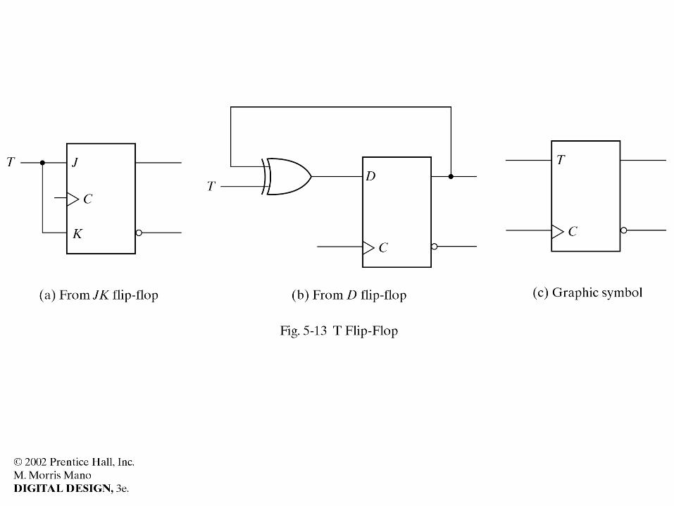
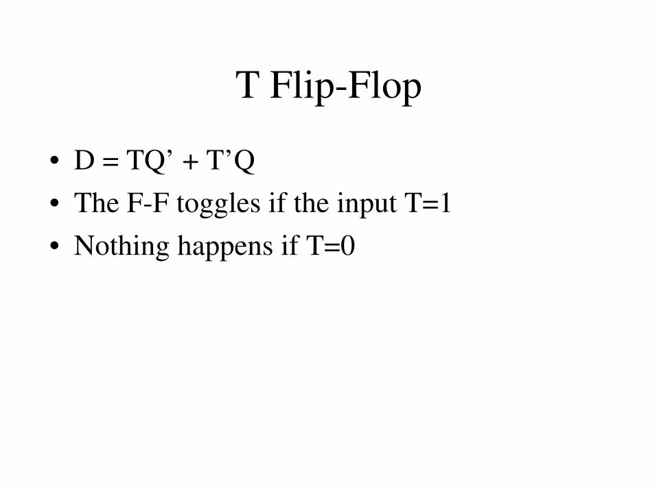
T FlipFlop
• D = TQ’ + T’Q• The FF toggles if the input T=1• Nothing happens if T=0
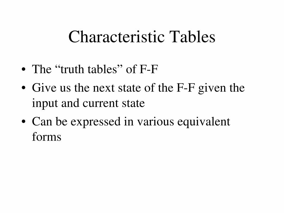
Characteristic Tables
• The “truth tables” of FF• Give us the next state of the FF given the
input and current state• Can be expressed in various equivalent
forms
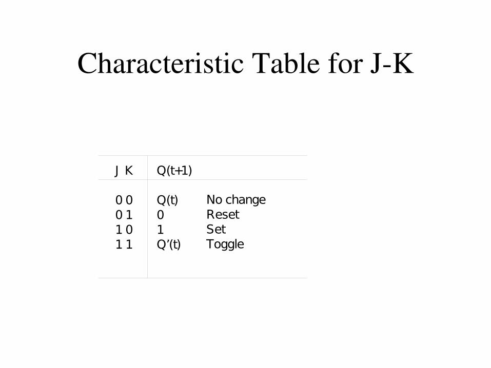
Characteristic Table for JK
J K
0 00 11 01 1
Q(t+1)
Q(t)01Q’(t)
No changeResetSetToggle
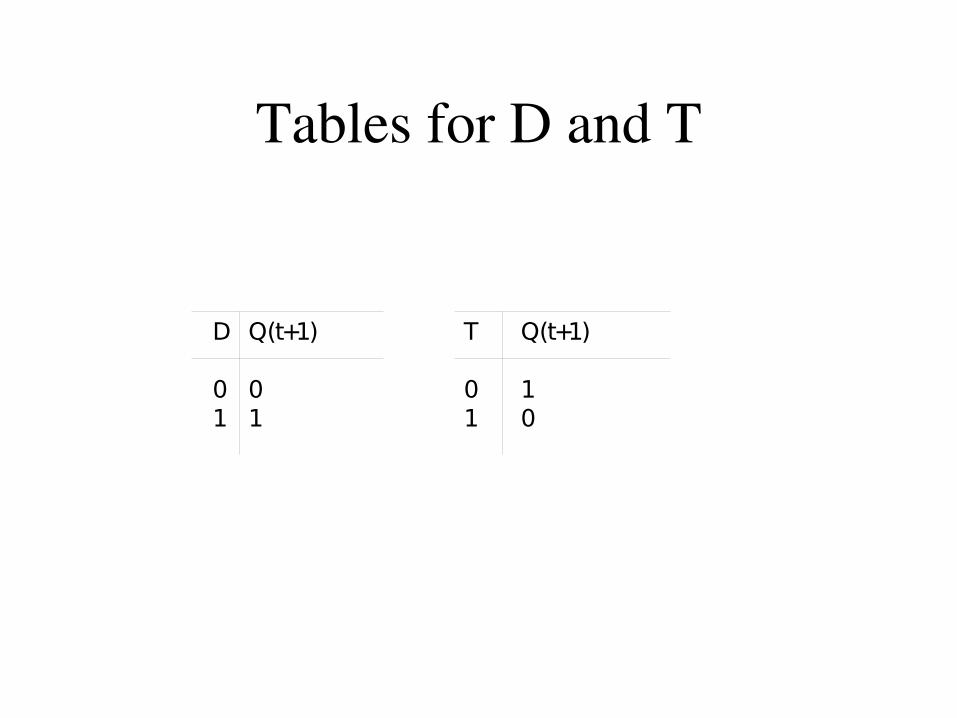
Tables for D and T
D
01
Q(t+1)
01
T
01
Q(t+1)
10
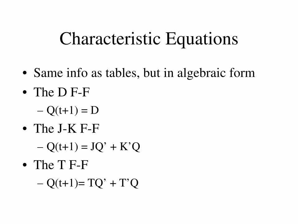
Characteristic Equations
• Same info as tables, but in algebraic form• The D FF
– Q(t+1) = D
• The JK FF– Q(t+1) = JQ’ + K’Q
• The T FF– Q(t+1)= TQ’ + T’Q
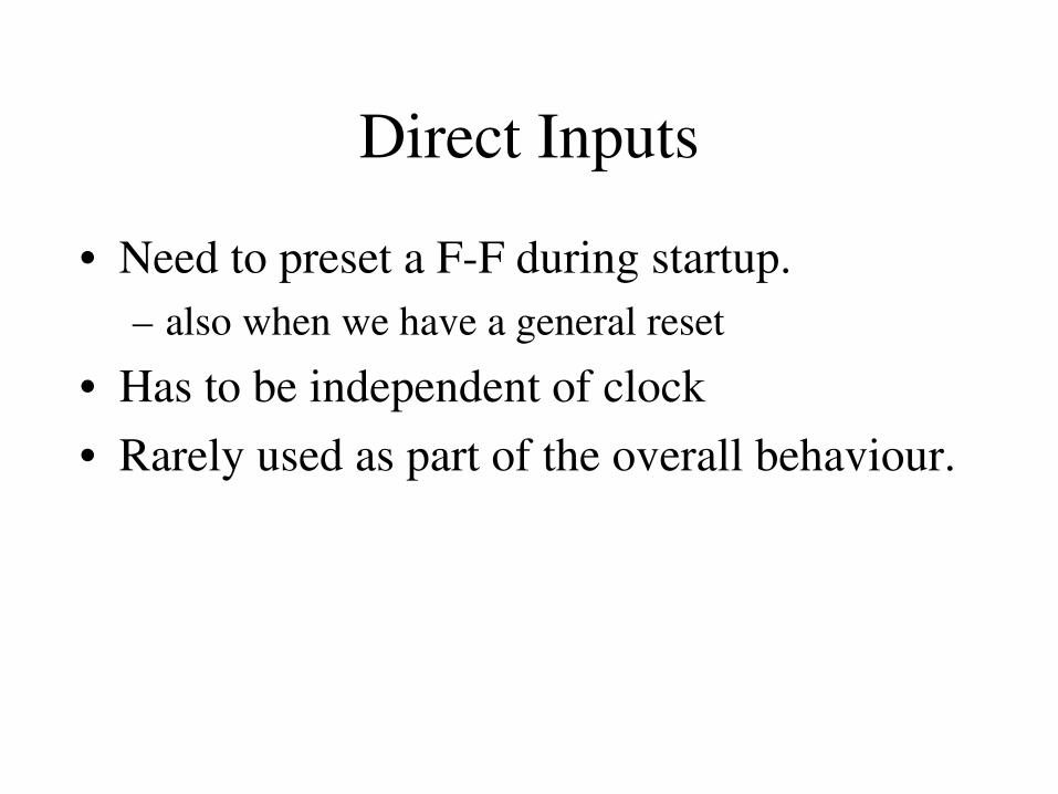
Direct Inputs
• Need to preset a FF during startup.– also when we have a general reset
• Has to be independent of clock• Rarely used as part of the overall behaviour.
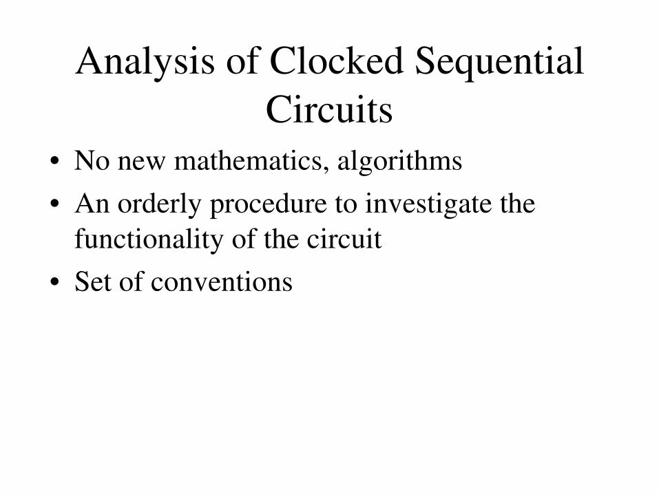
Analysis of Clocked Sequential Circuits
• No new mathematics, algorithms• An orderly procedure to investigate the
functionality of the circuit• Set of conventions
State Equations
• Every combination of the flipflop values is called state
• The state changes after every clock pulse• State equations are the equations that give us
the next state as a function of the current state and the input
State Equations
• The state equations are also called transition equations
• We derive the state equations from the circuit schematic
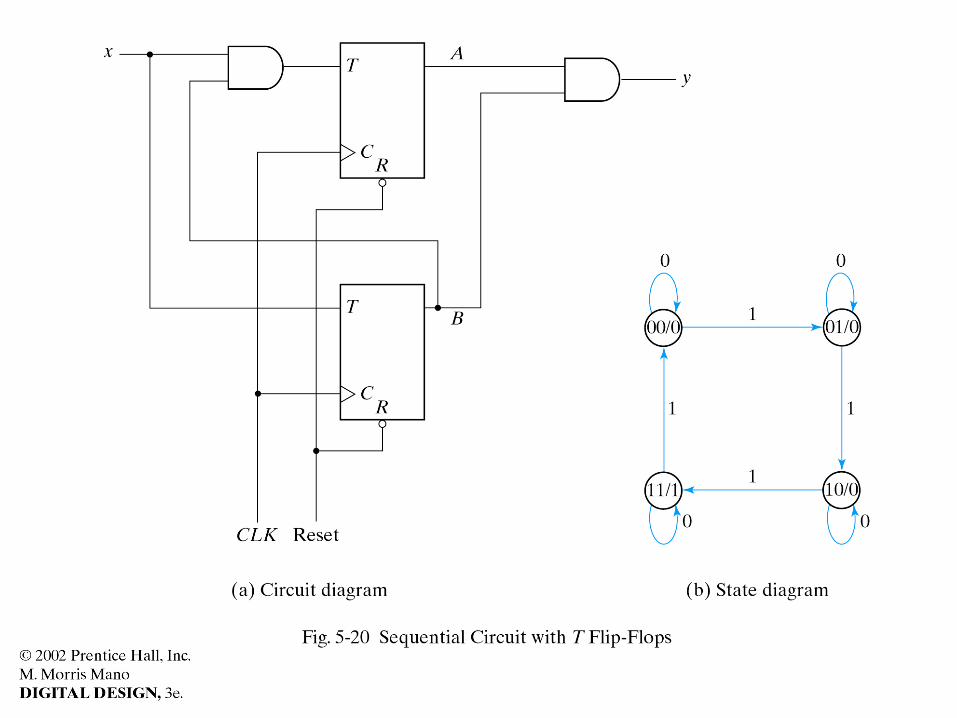
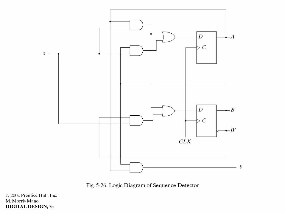
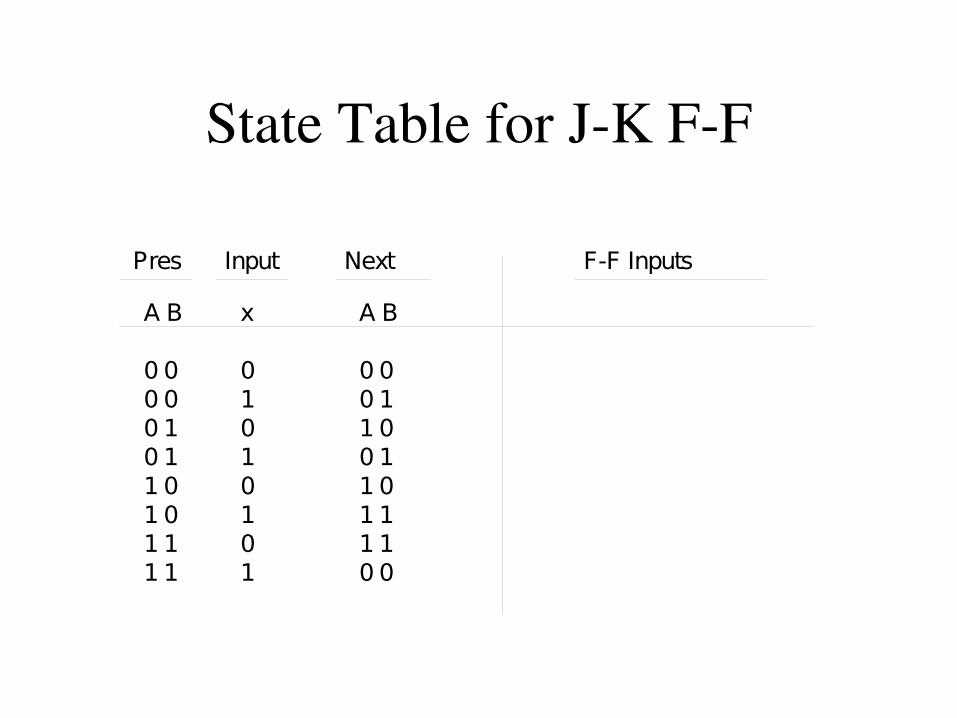
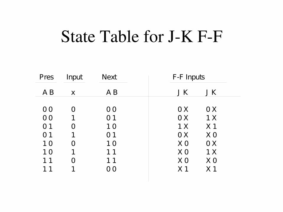
Example
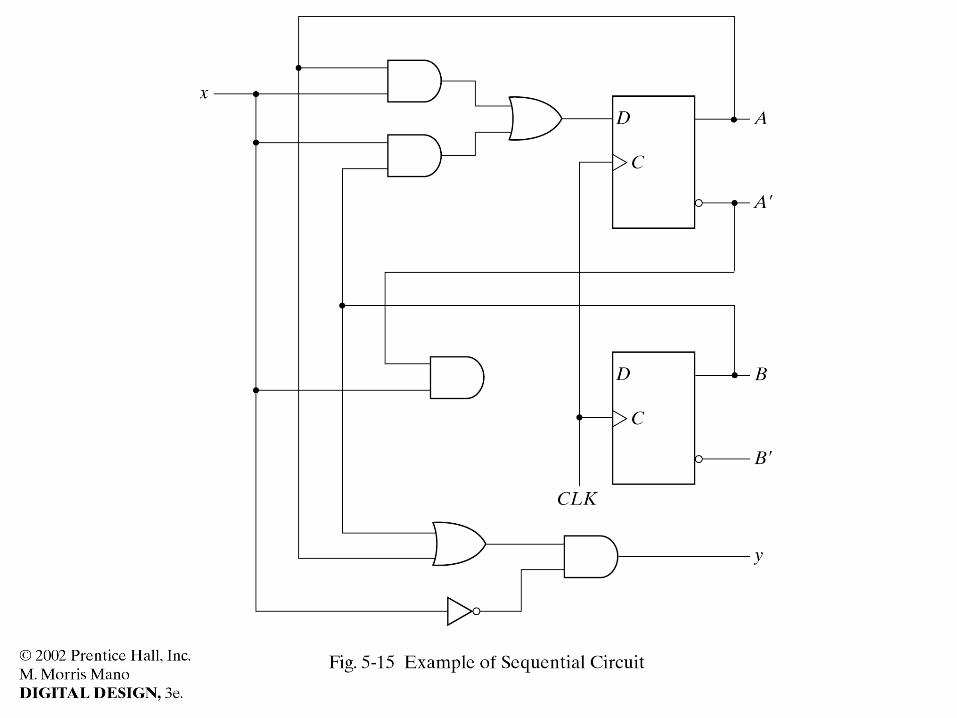
• We analyze a simple circuit with two FF named A and B, one input x and an output y
• We derive the state equations first
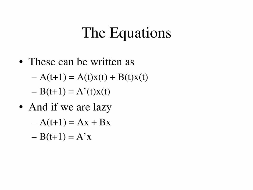
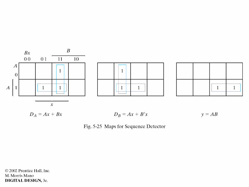
The Equations
• These can be written as– A(t+1) = A(t)x(t) + B(t)x(t)– B(t+1) = A’(t)x(t)
• And if we are lazy– A(t+1) = Ax + Bx– B(t+1) = A’x
Not done yet
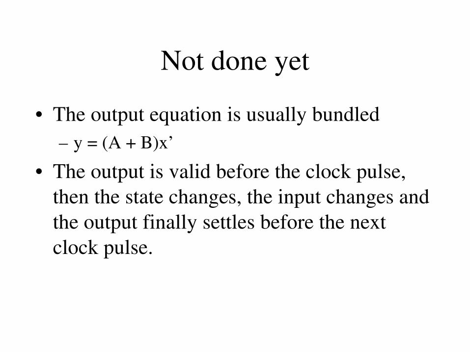
• The output equation is usually bundled– y = (A + B)x’
• The output is valid before the clock pulse, then the state changes, the input changes and the output finally settles before the next clock pulse.
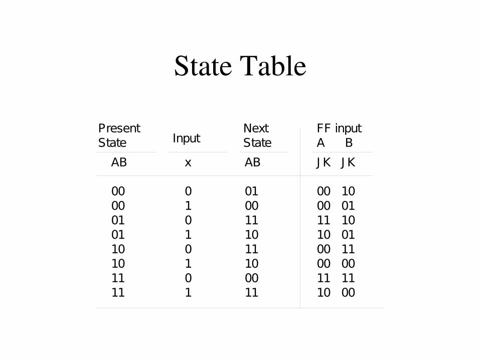
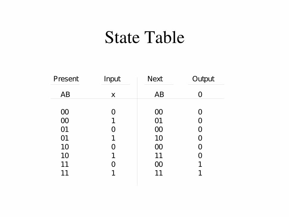
State Table
• The state table presents the same information in tabular form
• Also called transition table• Also bundled with the output data
Two Common Forms
• In the first form every row is labeled by all unique combinations of current state and input. The next state and output are separate columns
• In the second, we label rows with all current states and have multiple sets of columns for the next state and output.
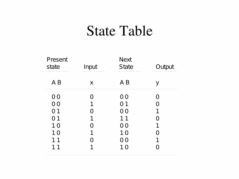
State Table
Presentstate Input
NextState Output
A B
0 00 00 10 11 01 01 11 1
x
01010101
A B
0 00 10 01 10 01 00 01 0
y
00101010
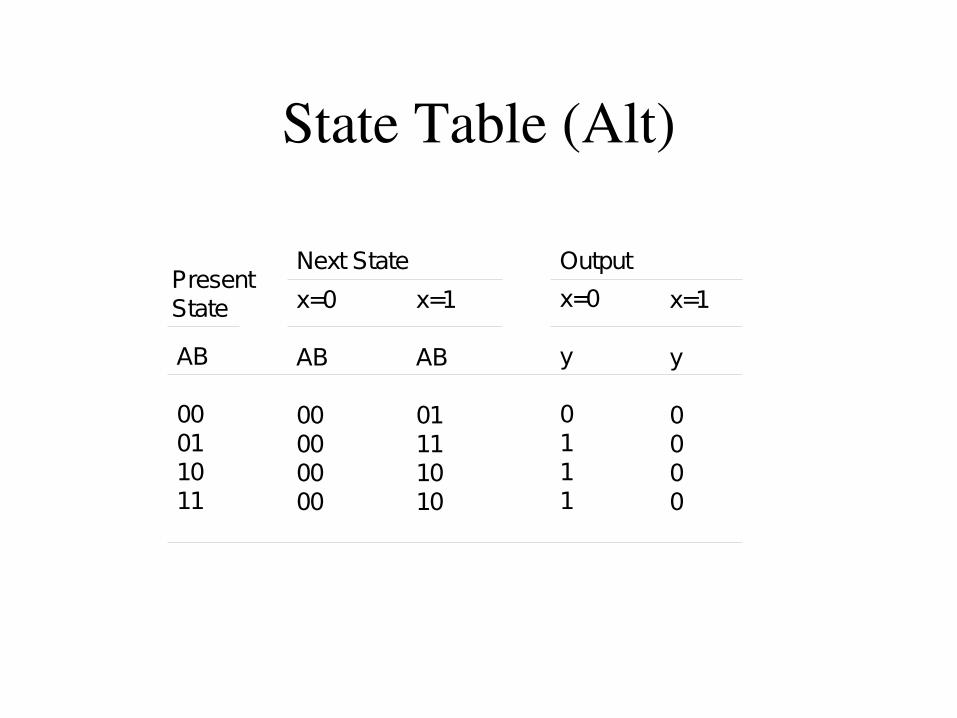
State Table (Alt)
PresentState
Next State Output
AB
00011011
x=0
AB
00000000
x=1
AB
01111010
x=0
y
0111
x=1
y
0000
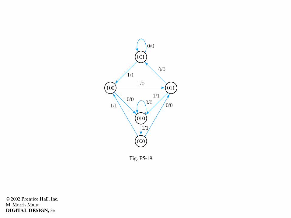
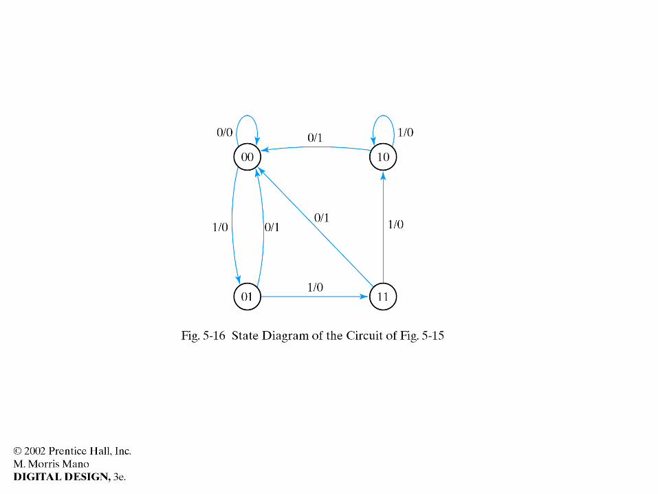
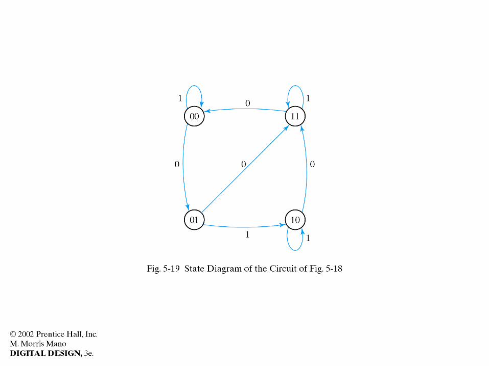
State Diagram
• We see the circuit more like something that changes states, than a collection of FF and gates
• It is really a Finite State Machine (FSM)• So can be represented by a State Diagram
(you know, the thingy with the bubbles and the arrows between them...)
State Diagram
• The bubbles represent the states and are labeled (usually) with the binary number of the state
• The edges are the transitions and are labeled with the input that cause the transition
• We indicate the output after the slash
Mealy and Moore
• There are two slight variations in FSMs– The Mealy, where the output is a function of the
input and present state– The Moore, where the output is a function of the
present state alone.
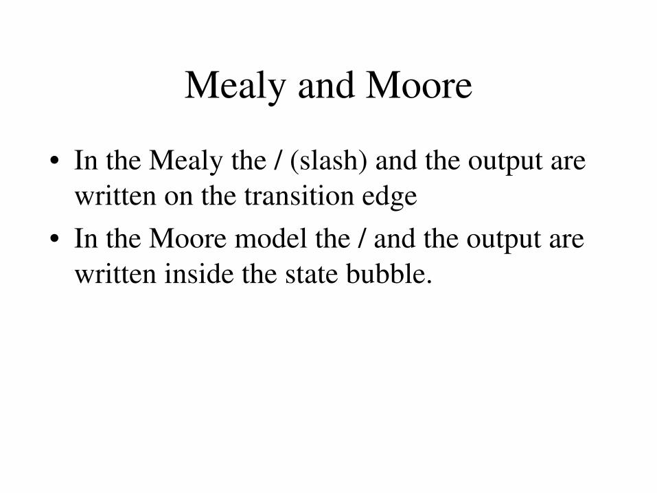
Mealy and Moore
• In the Mealy the / (slash) and the output are written on the transition edge
• In the Moore model the / and the output are written inside the state bubble.
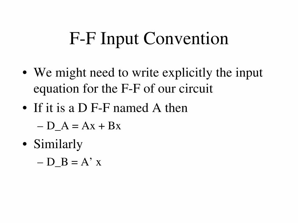
FF Input Convention
• We might need to write explicitly the input equation for the FF of our circuit
• If it is a D FF named A then– D_A = Ax + Bx
• Similarly– D_B = A’ x
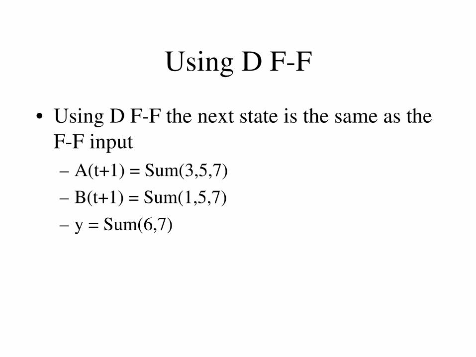
Analysis with D FF
• We did that already• It is easy because the next state is the same
as the input
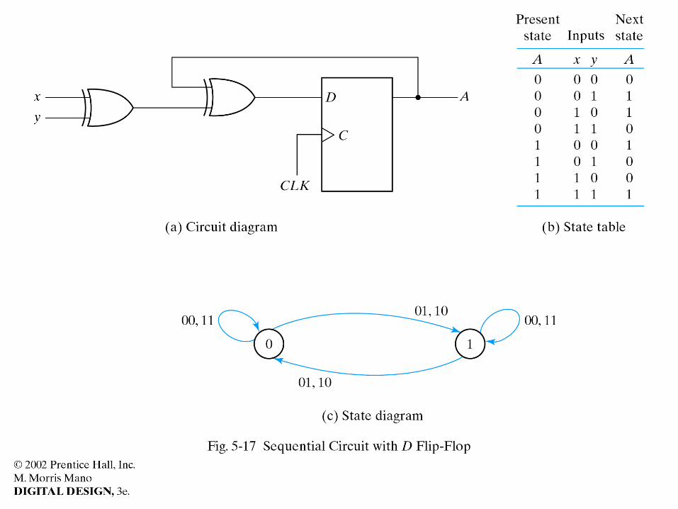
For this Example
• Input Equations– D_A = A xor x xor y
• State Equations– A(t+1) = A xor x xor y
• There is no output (the state itself is usually the output in this case)
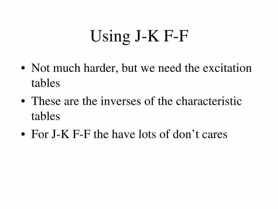
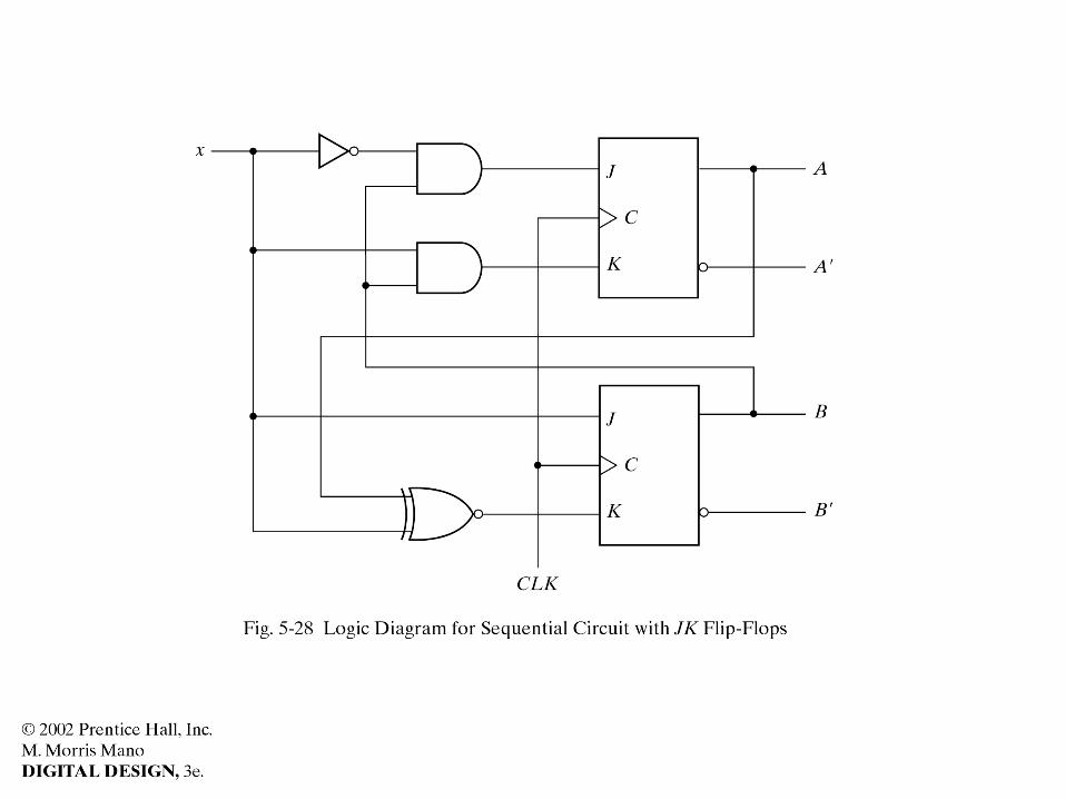
Analysis with JK FF
• Slightly more complex• One needs to use the characteristic table or
the characteristic equation for the JK FF
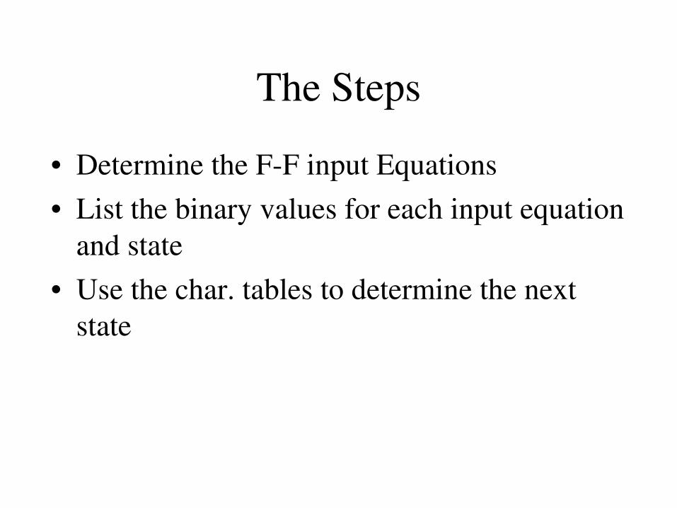
The Steps
• Determine the FF input Equations• List the binary values for each input equation
and state• Use the char. tables to determine the next
state
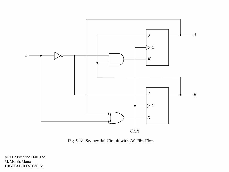
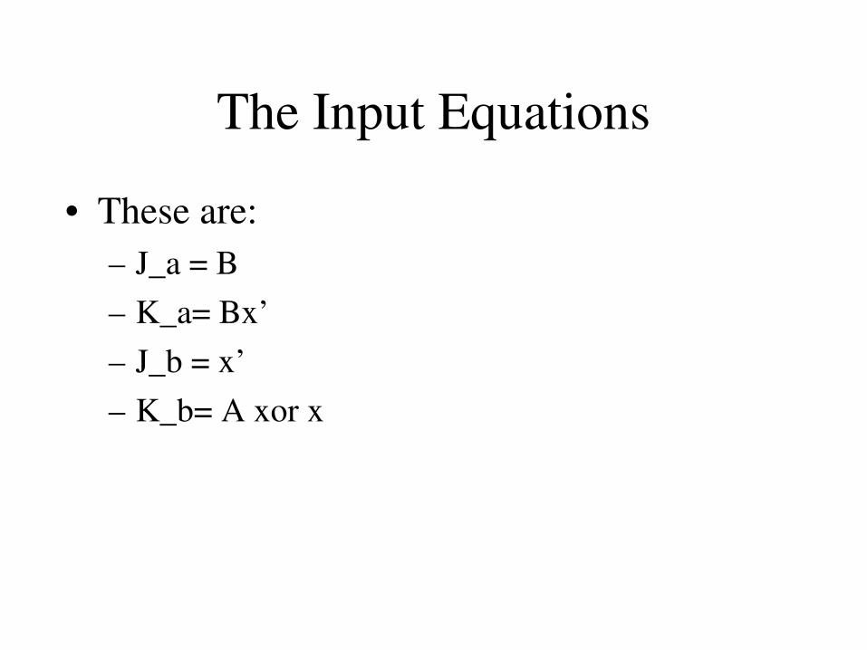
The Input Equations
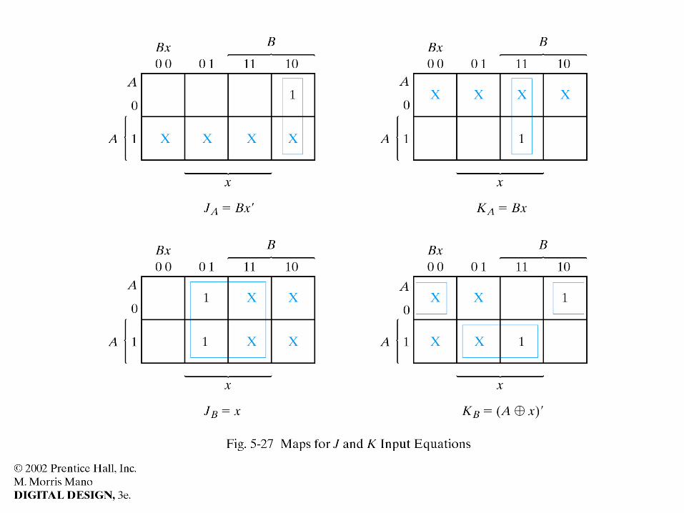
• These are:– J_a = B– K_a= Bx’– J_b = x’– K_b= A xor x
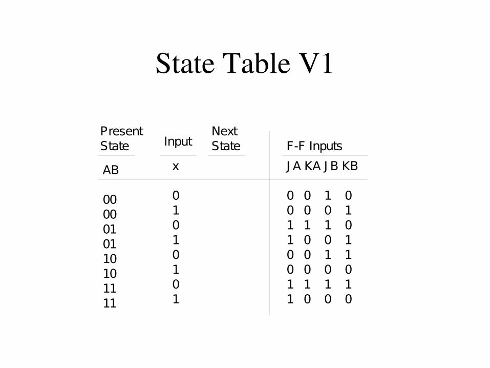
State Table V1
PresentState Input
NextState F-F Inputs
AB
0000010110101111
J A KA J B KB
0 0 1 00 0 0 11 1 1 01 0 0 10 0 1 10 0 0 01 1 1 11 0 0 0
x
01010101
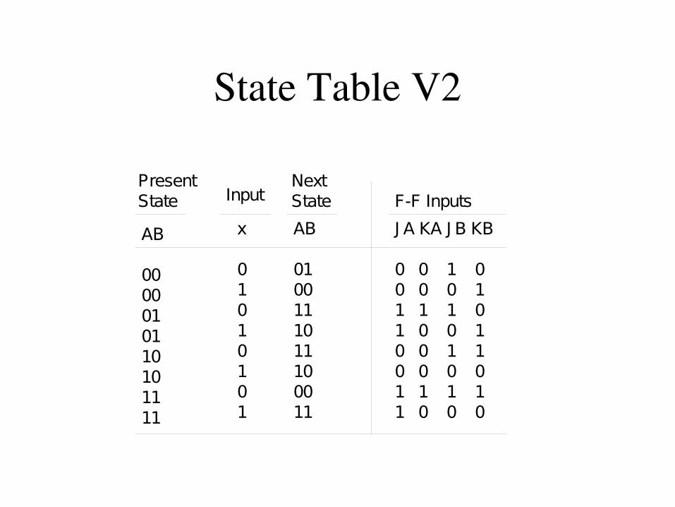
State Table V2
PresentState Input
NextState F-F Inputs
AB
0000010110101111
AB
0100111011100011
J A KA J B KB
0 0 1 00 0 0 11 1 1 01 0 0 10 0 1 10 0 0 01 1 1 11 0 0 0
x
01010101
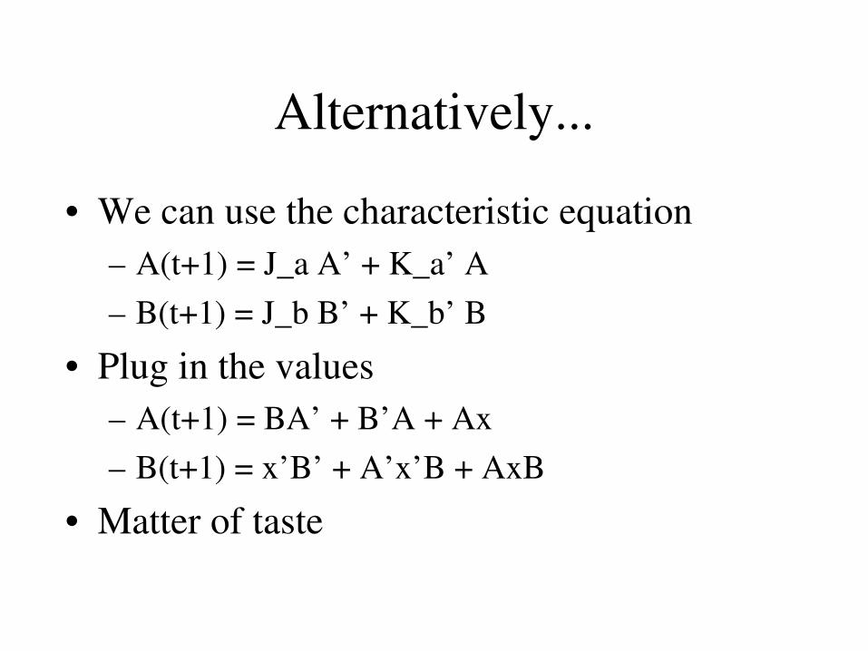
Alternatively...
• We can use the characteristic equation– A(t+1) = J_a A’ + K_a’ A– B(t+1) = J_b B’ + K_b’ B
• Plug in the values– A(t+1) = BA’ + B’A + Ax– B(t+1) = x’B’ + A’x’B + AxB
• Matter of taste
Analysis with T FF
• Similar idea to JK FF• We fill the state table in two stages
State Table
PresentState Input
NextState
FF inputA B
AB
0000010110101111
x
01010101
AB
0100111011100011
J K
0000111000001110
J K
1001100111001100
HDL for Sequential Circuits
• Behavioral Modeling– using the always construct
• Structural Description– By describing the interconnection between gates
and FFs

The always Construct
• The always statement is executed repeatedly
• Normally conditioned by the event control expression or sensitivity list or just @list
• Can have as many always statements as needed. All execute concurrently– Concurrency is a fact of life in H/W
The always Construct
• The event list is an or separated list of signals
• The always statement is executed when there is a change in any of the signals
• The statement (or block of statements) is then executed once
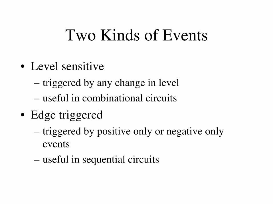
Two Kinds of Events
• Level sensitive– triggered by any change in level– useful in combinational circuits
• Edge triggered– triggered by positive only or negative only
events– useful in sequential circuits
Of course!
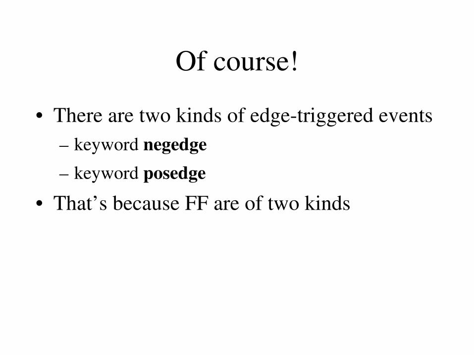
• There are two kinds of edgetriggered events– keyword negedge– keyword posedge
• That’s because FF are of two kinds
Procedural Assignments
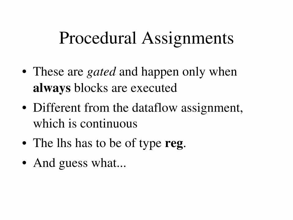
• These are gated and happen only when always blocks are executed
• Different from the dataflow assignment, which is continuous
• The lhs has to be of type reg.
• And guess what...
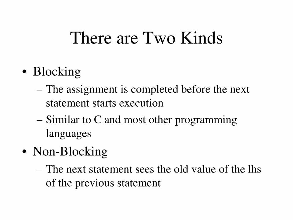
There are Two Kinds
• Blocking– The assignment is completed before the next
statement starts execution– Similar to C and most other programming
languages
• NonBlocking– The next statement sees the old value of the lhs
of the previous statement
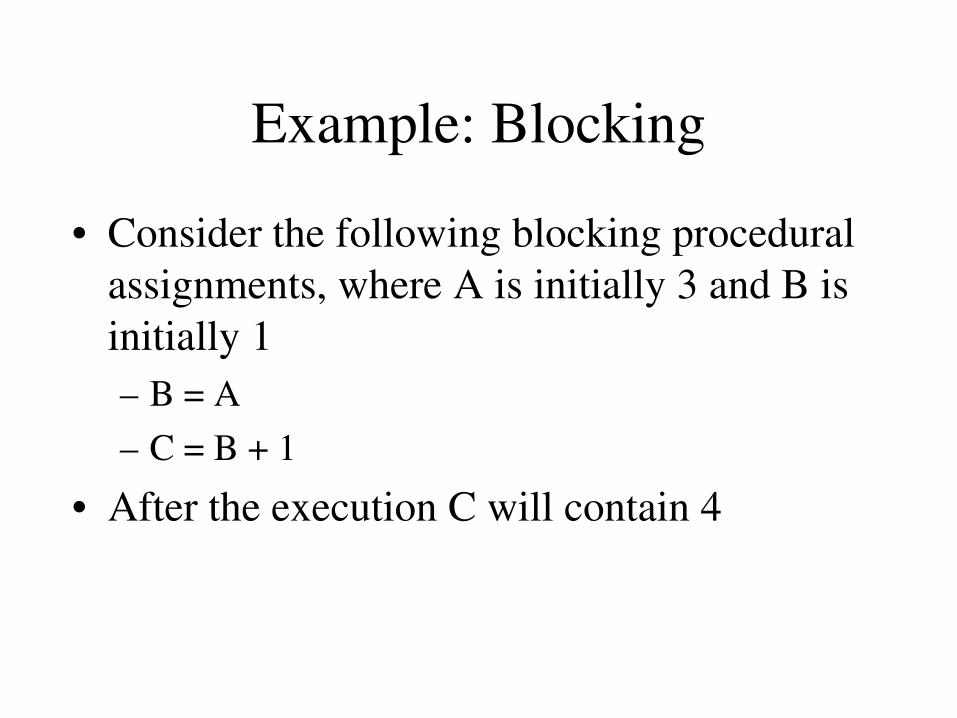
Example: Blocking
• Consider the following blocking procedural assignments, where A is initially 3 and B is initially 1– B = A– C = B + 1
• After the execution C will contain 4
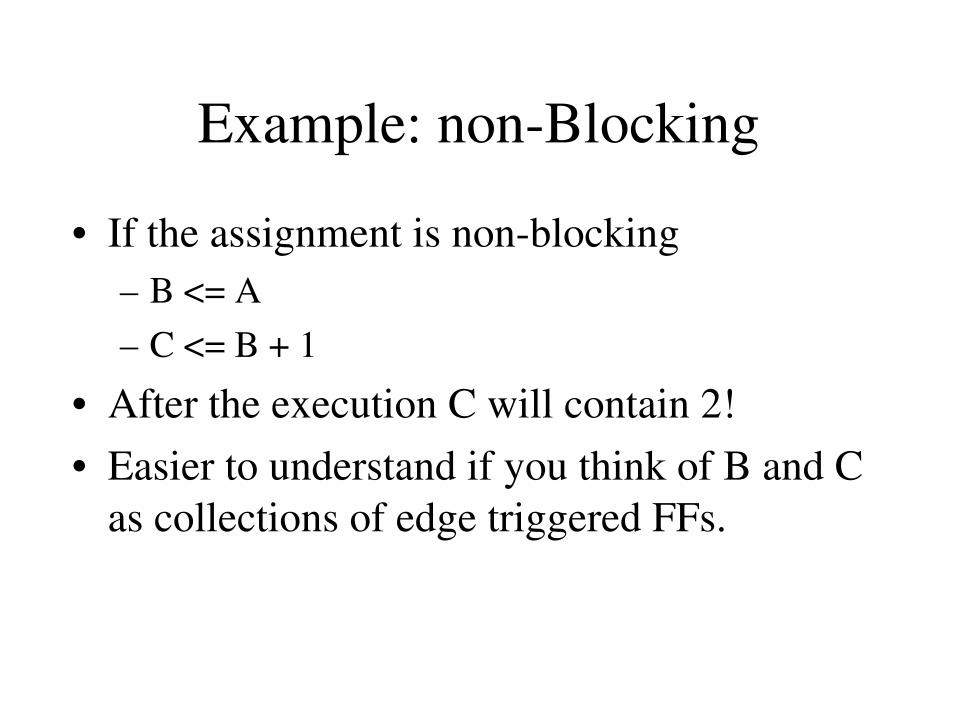
Example: nonBlocking
• If the assignment is nonblocking– B <= A– C <= B + 1
• After the execution C will contain 2!• Easier to understand if you think of B and C
as collections of edge triggered FFs.
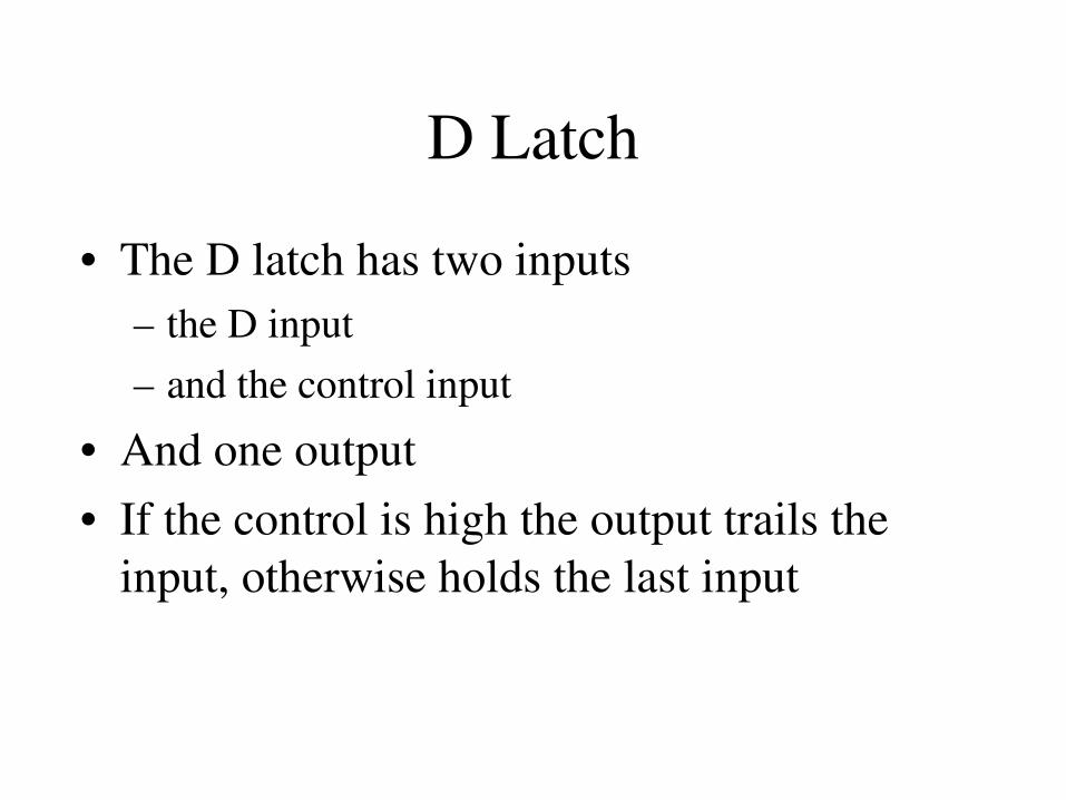
D Latch
• The D latch has two inputs– the D input– and the control input
• And one output• If the control is high the output trails the
input, otherwise holds the last input
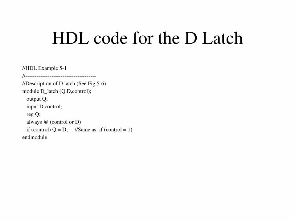
HDL code for the D Latch//HDL Example 51// //Description of D latch (See Fig.56)module D_latch (Q,D,control); output Q; input D,control; reg Q; always @ (control or D) if (control) Q = D; //Same as: if (control = 1)endmodule
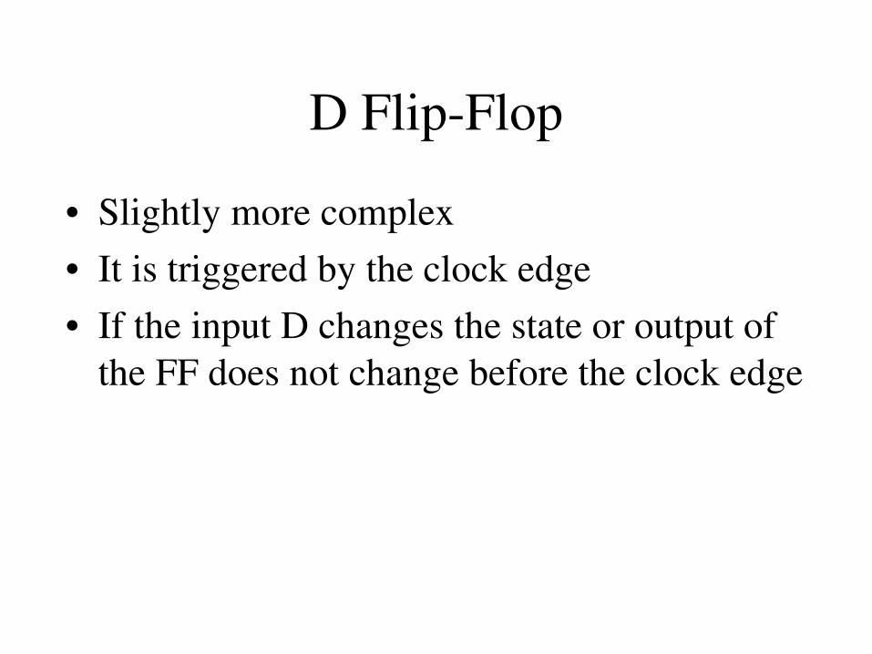
D FlipFlop
• Slightly more complex• It is triggered by the clock edge• If the input D changes the state or output of
the FF does not change before the clock edge
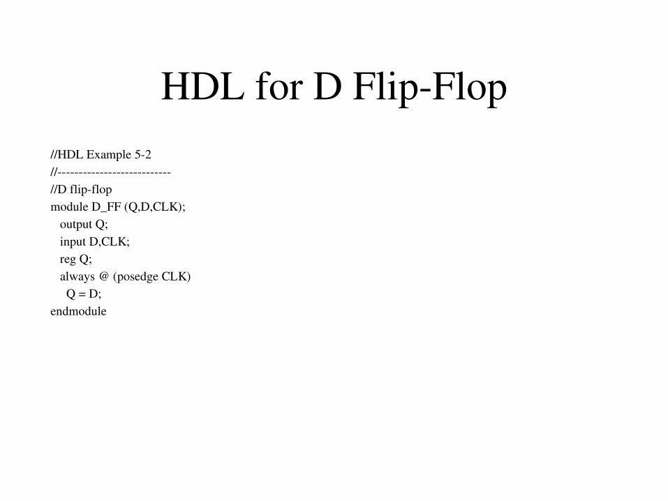
HDL for D FlipFlop//HDL Example 52// //D flipflop module D_FF (Q,D,CLK); output Q; input D,CLK; reg Q; always @ (posedge CLK) Q = D;endmodule
D FF with RESET
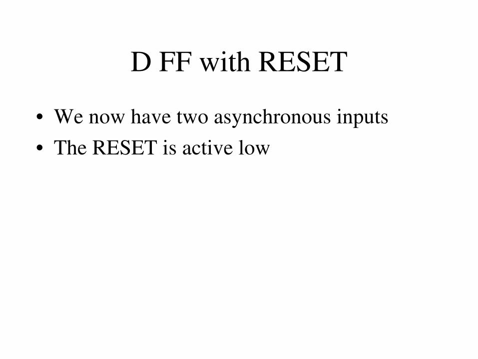
• We now have two asynchronous inputs• The RESET is active low
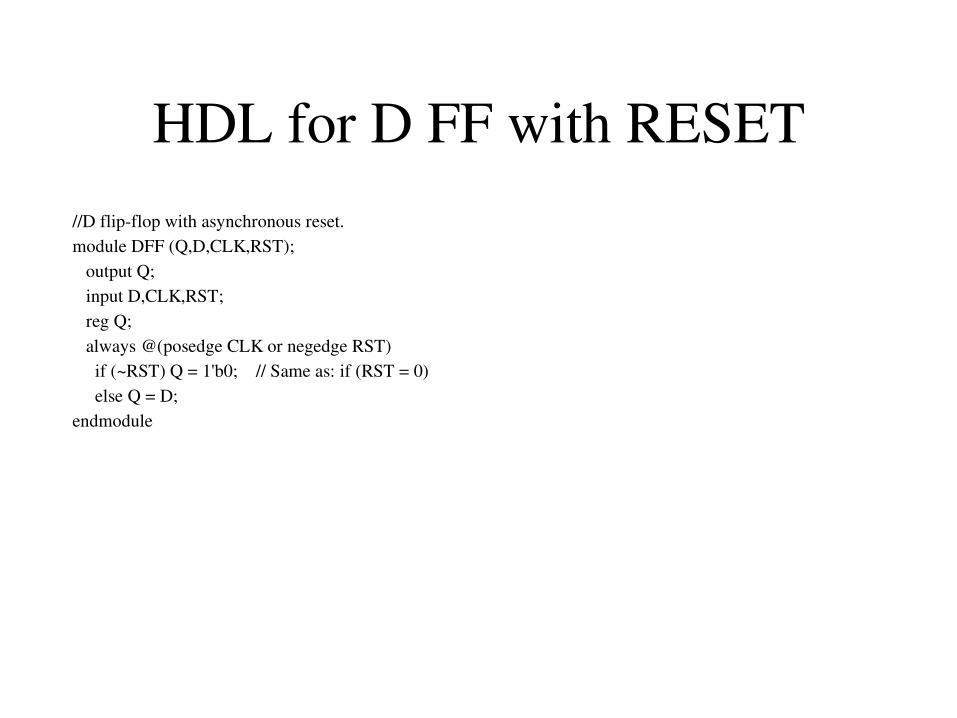
HDL for D FF with RESET//D flipflop with asynchronous reset.module DFF (Q,D,CLK,RST); output Q; input D,CLK,RST; reg Q; always @(posedge CLK or negedge RST) if (~RST) Q = 1'b0; // Same as: if (RST = 0) else Q = D;endmodule
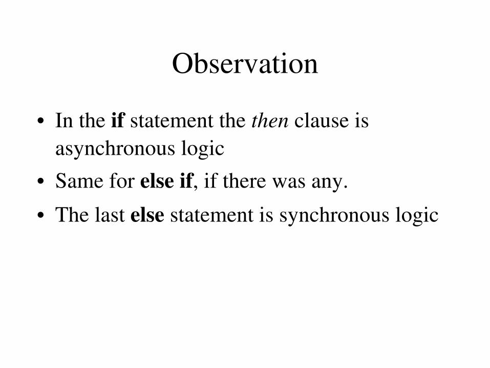
Observation
• In the if statement the then clause is asynchronous logic
• Same for else if, if there was any.
• The last else statement is synchronous logic
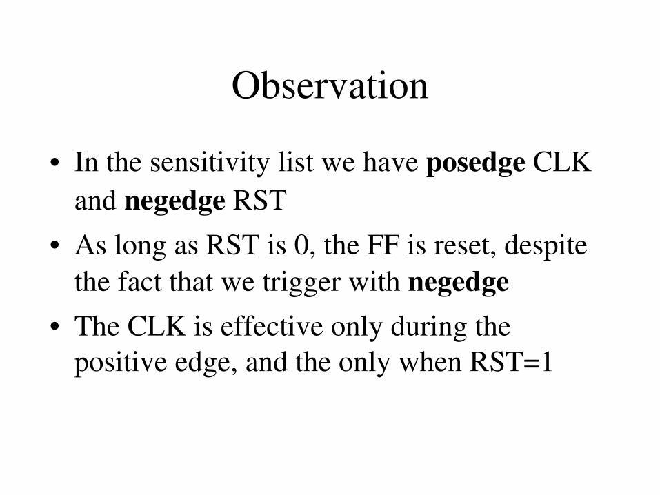
Observation
• In the sensitivity list we have posedge CLK and negedge RST
• As long as RST is 0, the FF is reset, despite the fact that we trigger with negedge
• The CLK is effective only during the positive edge, and the only when RST=1
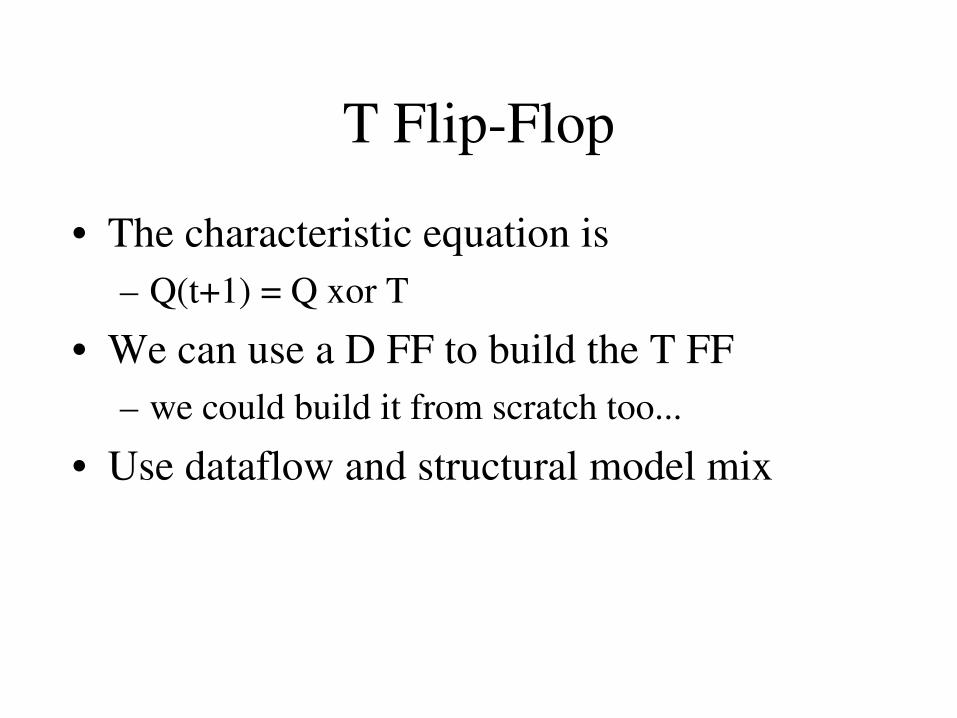
T FlipFlop
• The characteristic equation is– Q(t+1) = Q xor T
• We can use a D FF to build the T FF– we could build it from scratch too...
• Use dataflow and structural model mix
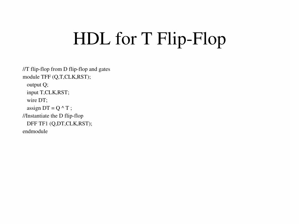
HDL for T FlipFlop//T flipflop from D flipflop and gatesmodule TFF (Q,T,CLK,RST); output Q; input T,CLK,RST; wire DT; assign DT = Q ^ T ;//Instantiate the D flipflop DFF TF1 (Q,DT,CLK,RST);endmodule
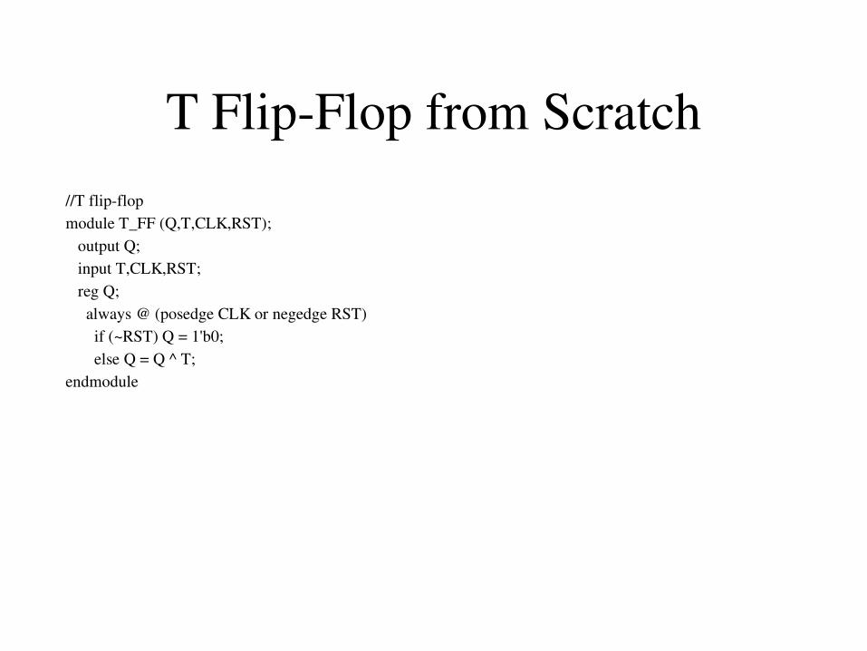
T FlipFlop from Scratch//T flipflopmodule T_FF (Q,T,CLK,RST); output Q; input T,CLK,RST; reg Q; always @ (posedge CLK or negedge RST) if (~RST) Q = 1'b0; else Q = Q ^ T;endmodule
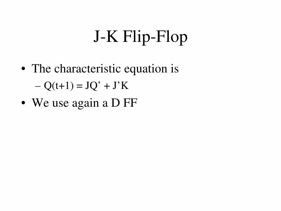
JK FlipFlop
• The characteristic equation is– Q(t+1) = JQ’ + J’K
• We use again a D FF
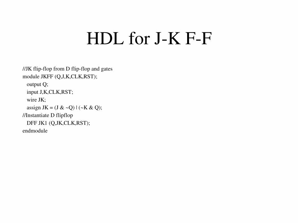
HDL for JK FF//JK flipflop from D flipflop and gates module JKFF (Q,J,K,CLK,RST); output Q; input J,K,CLK,RST; wire JK; assign JK = (J & ~Q) | (~K & Q);//Instantiate D flipflop DFF JK1 (Q,JK,CLK,RST);endmodule
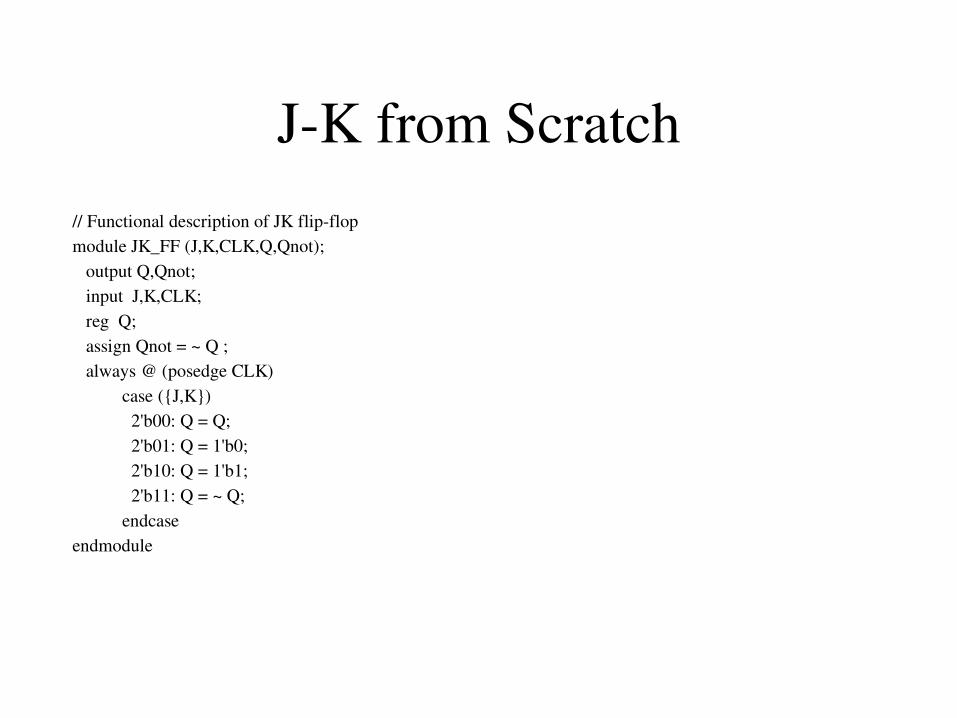
JK from Scratch// Functional description of JK flipflopmodule JK_FF (J,K,CLK,Q,Qnot); output Q,Qnot; input J,K,CLK; reg Q; assign Qnot = ~ Q ; always @ (posedge CLK) case ({J,K}) 2'b00: Q = Q; 2'b01: Q = 1'b0; 2'b10: Q = 1'b1; 2'b11: Q = ~ Q; endcaseendmodule
State Diagrams
• Verilog (and other HDLs) can immitate state diagrams
• There are two basic variations: Mealy and Moore
• Makes life easier to use keyword parameter.
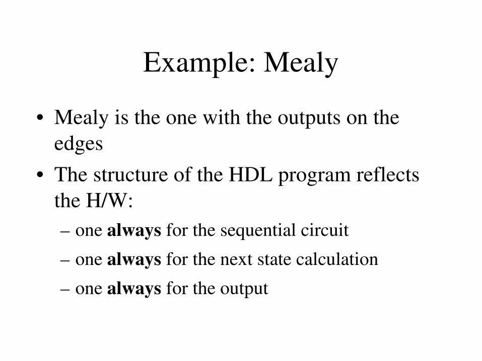
Example: Mealy
• Mealy is the one with the outputs on the edges
• The structure of the HDL program reflects the H/W:– one always for the sequential circuit
– one always for the next state calculation
– one always for the output
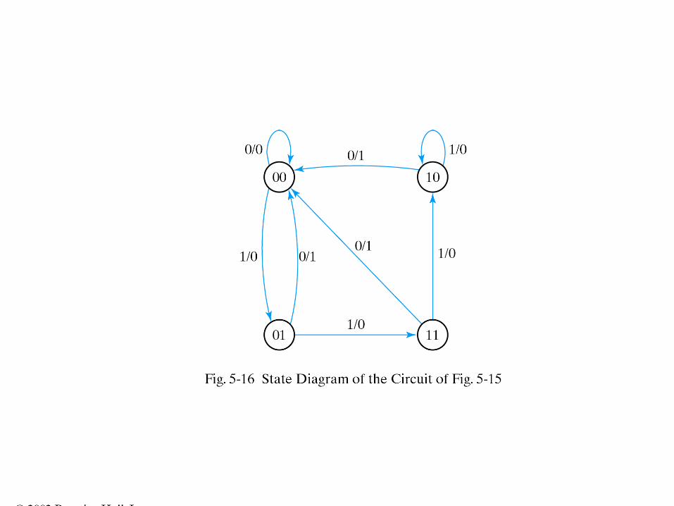
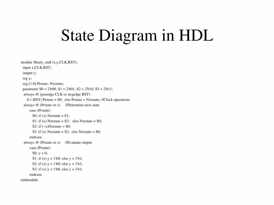
State Diagram in HDLmodule Mealy_mdl (x,y,CLK,RST); input x,CLK,RST; output y; reg y; reg [1:0] Prstate, Nxtstate; parameter S0 = 2'b00, S1 = 2'b01, S2 = 2'b10, S3 = 2'b11; always @ (posedge CLK or negedge RST) if (~RST) Prstate = S0; else Prstate = Nxtstate; //Clock operations always @ (Prstate or x) //Determine next state case (Prstate) S0: if (x) Nxtstate = S1; S1: if (x) Nxtstate = S3; else Nxtstate = S0; S2: if (~x)Nxtstate = S0; S3: if (x) Nxtstate = S2; else Nxtstate = S0; endcase always @ (Prstate or x) //Evaluate output case (Prstate) S0: y = 0; S1: if (x) y = 1'b0; else y = 1'b1; S2: if (x) y = 1'b0; else y = 1'b1; S3: if (x) y = 1'b0; else y = 1'b1; endcaseendmodule
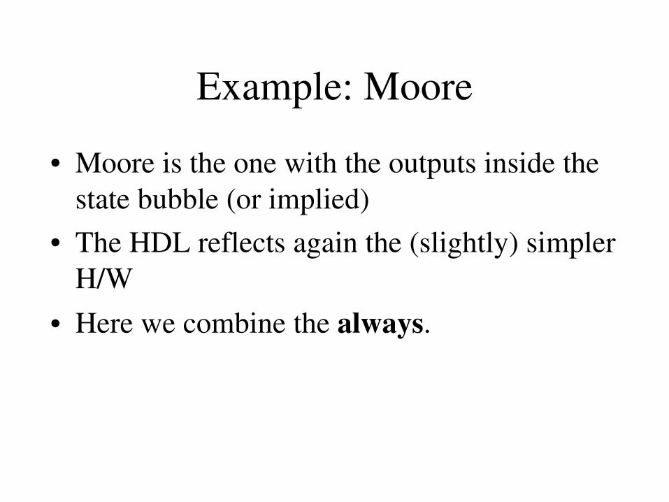
Example: Moore
• Moore is the one with the outputs inside the state bubble (or implied)
• The HDL reflects again the (slightly) simpler H/W
• Here we combine the always.
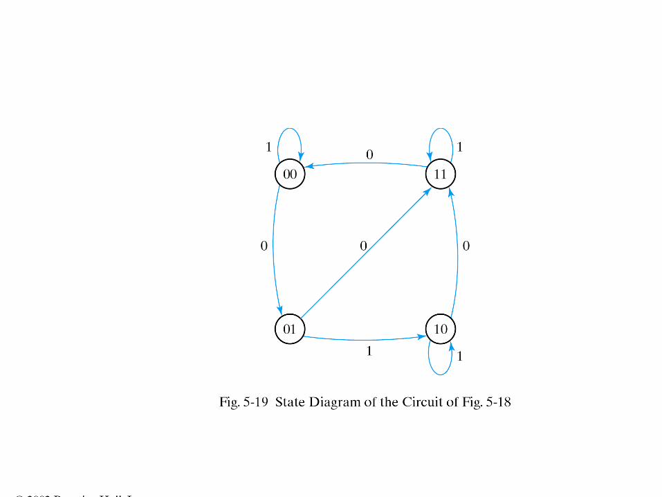
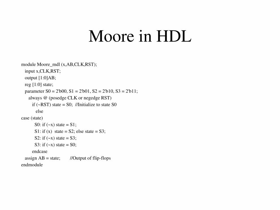
Moore in HDLmodule Moore_mdl (x,AB,CLK,RST); input x,CLK,RST; output [1:0]AB; reg [1:0] state; parameter S0 = 2'b00, S1 = 2'b01, S2 = 2'b10, S3 = 2'b11; always @ (posedge CLK or negedge RST) if (~RST) state = S0; //Initialize to state S0 elsecase (state) S0: if (~x) state = S1; S1: if (x) state = S2; else state = S3; S2: if (~x) state = S3; S3: if (~x) state = S0; endcase assign AB = state; //Output of flipflopsendmodule
State Reduction
• Often a sequential circuit with fewer states can do exactly the same job
• There are multiple benefits from reducing the number of states
• State tables (or diagrams) generated by software tend to have redundant states.
The Benefits
• Fewer flipflops• More unused states, thus more don’t cares
Definition
• Two FSM are equivalent when for all input sequences they produce the same output
• Unfortunately all is too many• We have to find a more workable definition
How About...
• Define the equivalence of states. If we find that two states are equivalent we merge them
• Two states in an FSM are equivalent if for every input produce the same output and jump to the same state or to equivalent states.
Sounds better
• This is a workable definition• We can use it to simplify state diagrams by
hand• We can use it to design an algorithm.
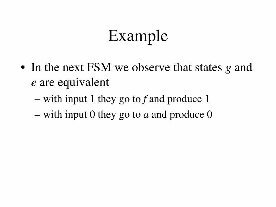
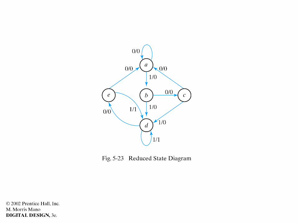
Example
• In the next FSM we observe that states g and e are equivalent– with input 1 they go to f and produce 1– with input 0 they go to a and produce 0
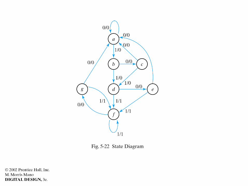
Some More...
• So e and g is one state with two different names.
• But now f and d are equivalent– with input 0 they go to {e,g} and produce 0– with input 1 they go to f and produce 1
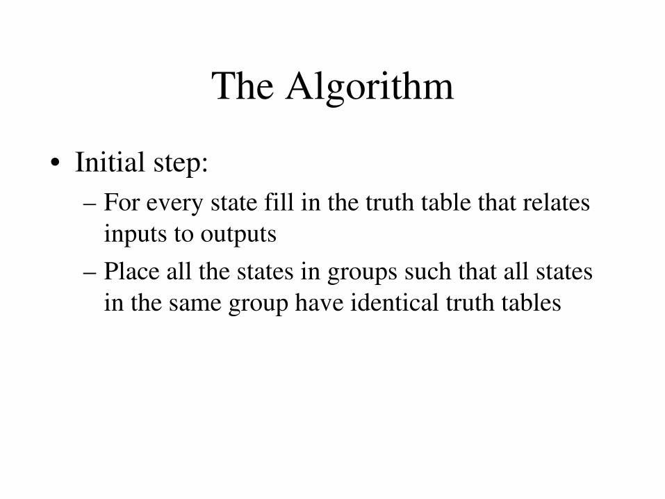
The Algorithm
• Initial step:– For every state fill in the truth table that relates
inputs to outputs– Place all the states in groups such that all states
in the same group have identical truth tables
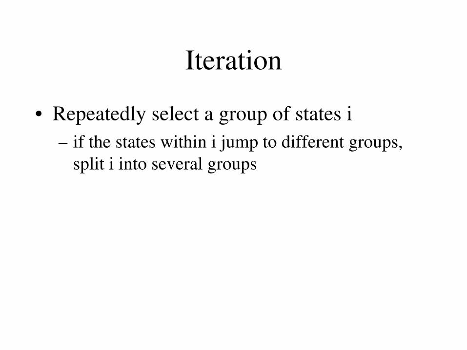
Iteration
• Repeatedly select a group of states i– if the states within i jump to different groups,
split i into several groups
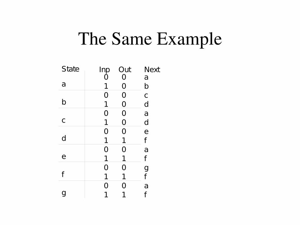
The Same Example
a
b
c
d
e
f
g
00000001010101
01010101010101
abcdadefafgfaf
State Inp Out Next
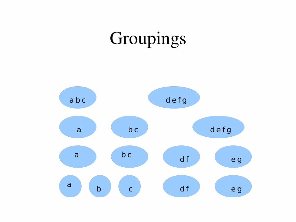
Groupings
d e f g
a
b c
d e f g
a b c
a
a
b c
b c
d f e g
e gd f
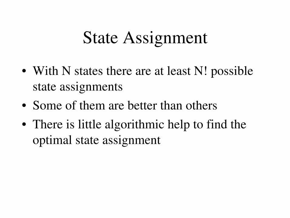
State Assignment
• With N states there are at least N! possible state assignments
• Some of them are better than others• There is little algorithmic help to find the
optimal state assignment
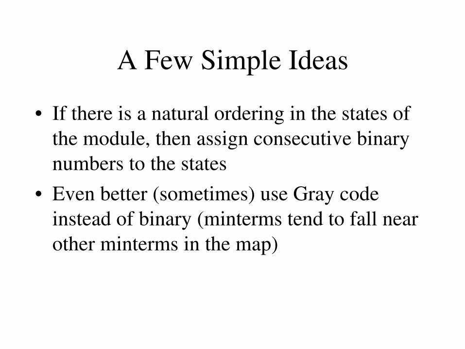
A Few Simple Ideas
• If there is a natural ordering in the states of the module, then assign consecutive binary numbers to the states
• Even better (sometimes) use Gray code instead of binary (minterms tend to fall near other minterms in the map)
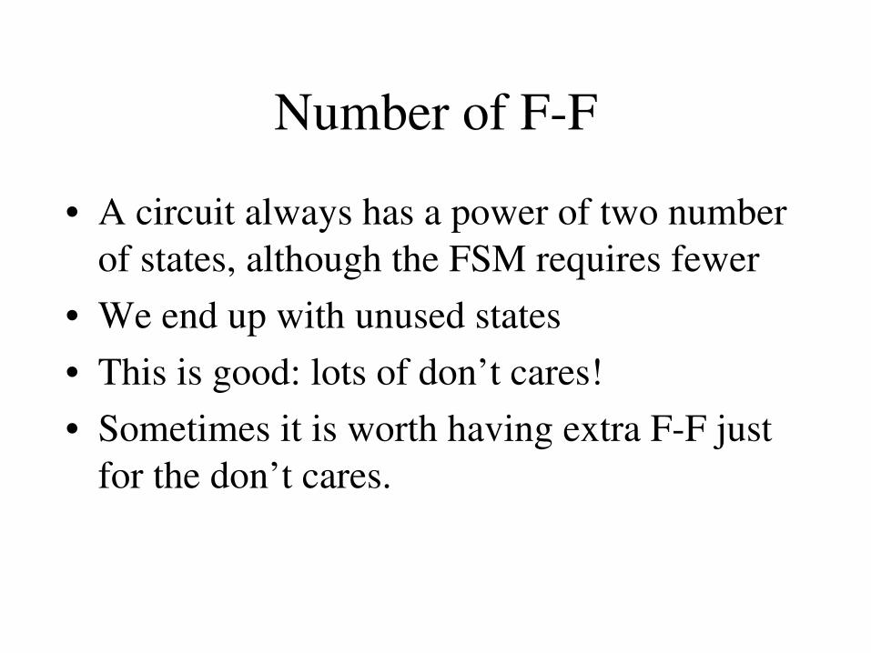
Number of FF
• A circuit always has a power of two number of states, although the FSM requires fewer
• We end up with unused states• This is good: lots of don’t cares!• Sometimes it is worth having extra FF just
for the don’t cares.
In the Extreme
• We can even have one FF per state (aka one hot)
• This often saves enough gates to justify the real estate taken up by the extra FF
Design Procedure
• Now we are ready to design a circuit• Design consists of
– translating “words” to symbols, tables, HDL...– specifying the logic– optimizing the design for cost and or
performance– communicating the results
But most of all
• Keep things tidy and ordered• Manage complexity
Detailed Steps
• Produce a state diagram• Minimize it• Assign binary values to states• Choose the technology• Obtain state table (binary coded)• Minimize FF input equations
...Detailed Steps
• Draw logic diagram (or equivalent)• Calculate costs• Do it again until you nauseate (or have
reduced the cost enough)
Word Specification
• Comes from the system architect• Might or might not be exact, unambiguous• There is some help from various design aids• Needs experience
Example
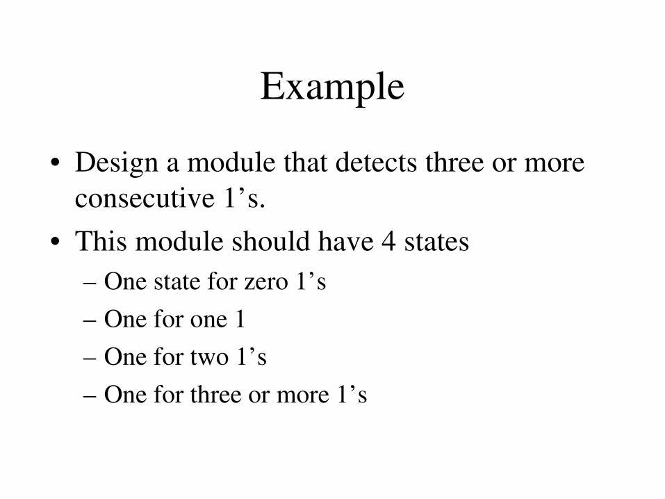
• Design a module that detects three or more consecutive 1’s.
• This module should have 4 states– One state for zero 1’s– One for one 1– One for two 1’s– One for three or more 1’s
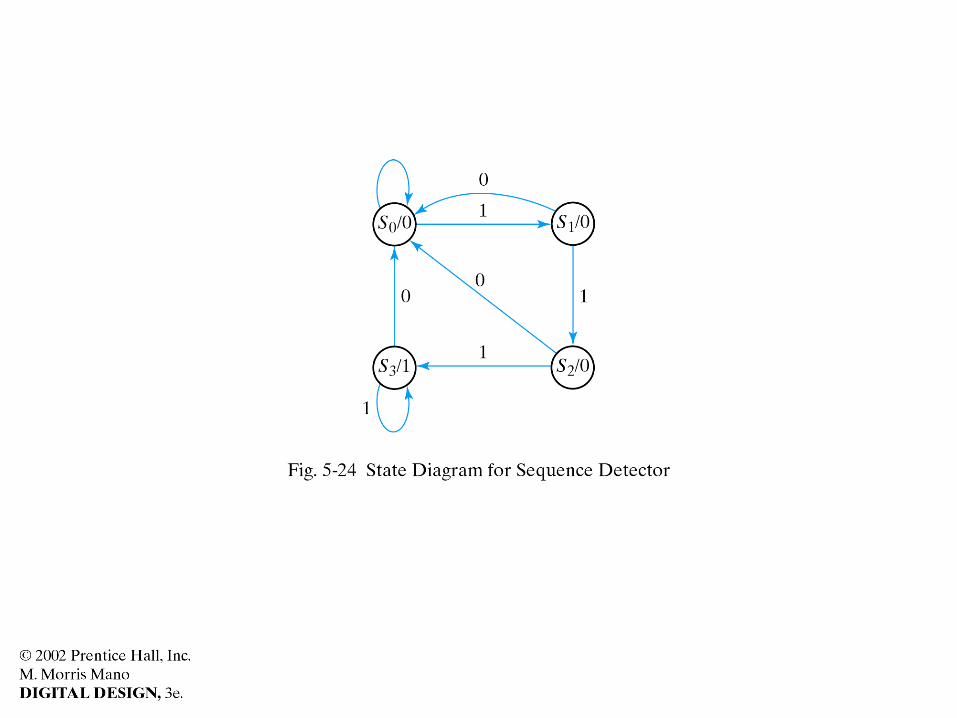
State Table
Present Input Next Output
AB
0000010110101111
x
01010101
AB
0001001000110011
0
00000011
Using D FF
• Using D FF the next state is the same as the FF input– A(t+1) = Sum(3,5,7)– B(t+1) = Sum(1,5,7)– y = Sum(6,7)
Using JK FF
• Not much harder, but we need the excitation tables
• These are the inverses of the characteristic tables
• For JK FF the have lots of don’t cares
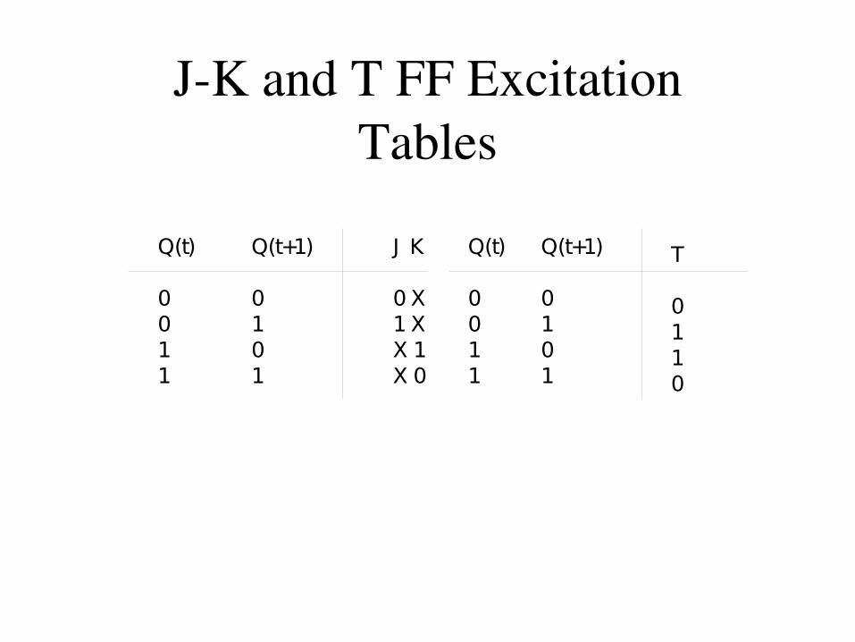
JK and T FF ExcitationTables
Q(t)
0011
Q(t+1)
0101
J K
0 X1 XX 1X 0
Q(t)
0011
Q(t+1)
0101
T
0110
State Table for JK FF
Pres Input Next F-F Inputs
A B
0 00 00 10 11 01 01 11 1
x
01010101
A B
0 00 11 00 11 01 11 10 0
State Table for JK FF
Pres Input Next F-F Inputs
A B
0 00 00 10 11 01 01 11 1
x
01010101
J K
0 X0 X1 X0 XX 0X 0X 0X 1
J K
0 X1 XX 1X 00 X1 XX 0X 1
A B
0 00 11 00 11 01 11 10 0
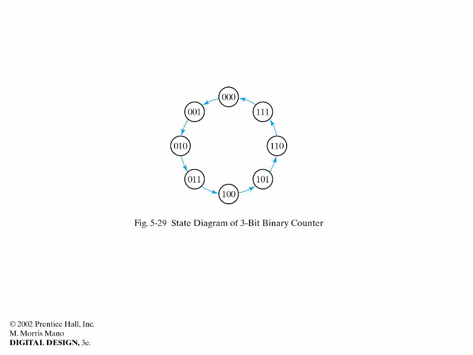
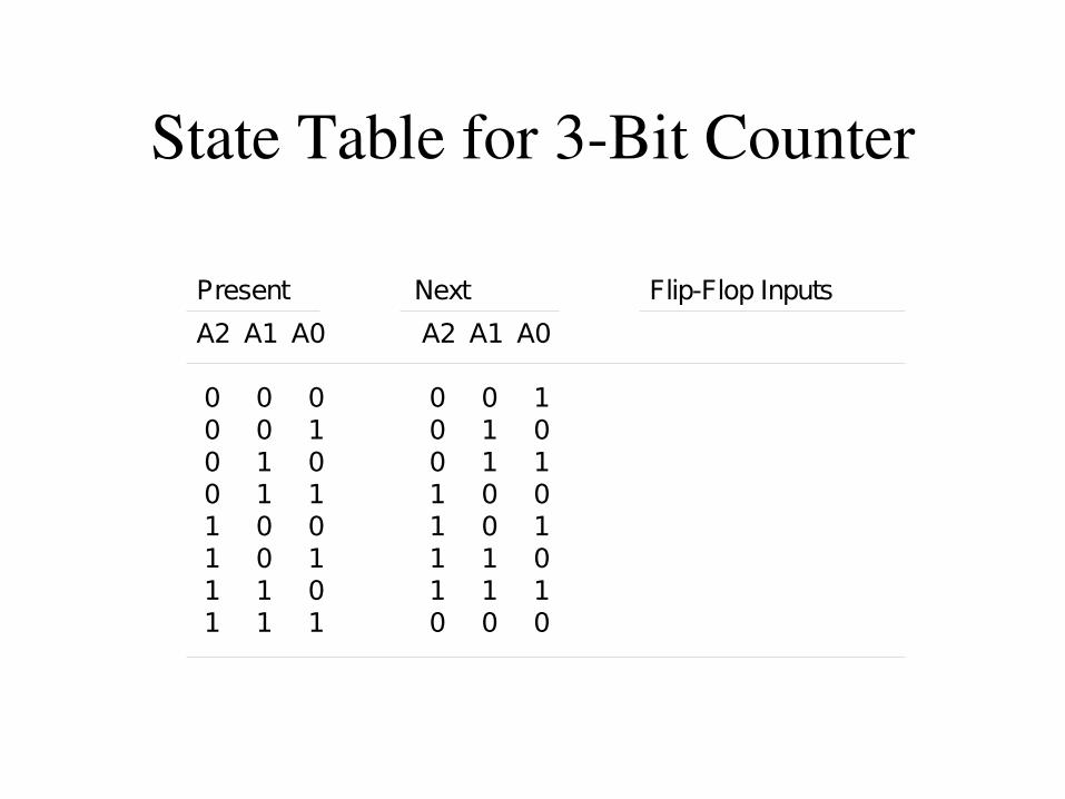
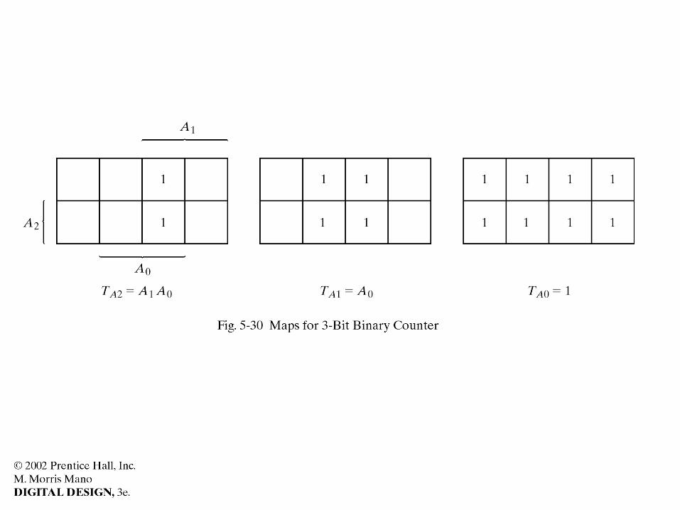
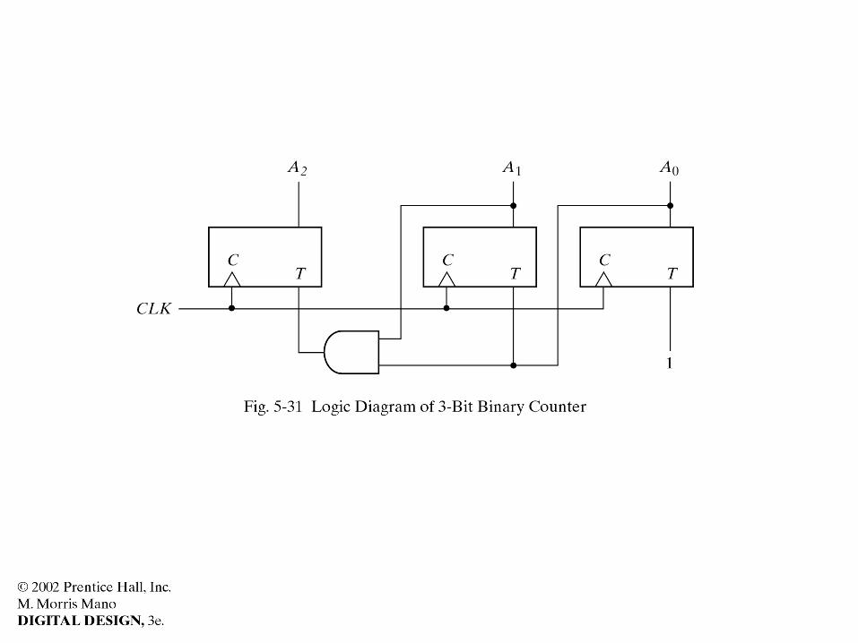
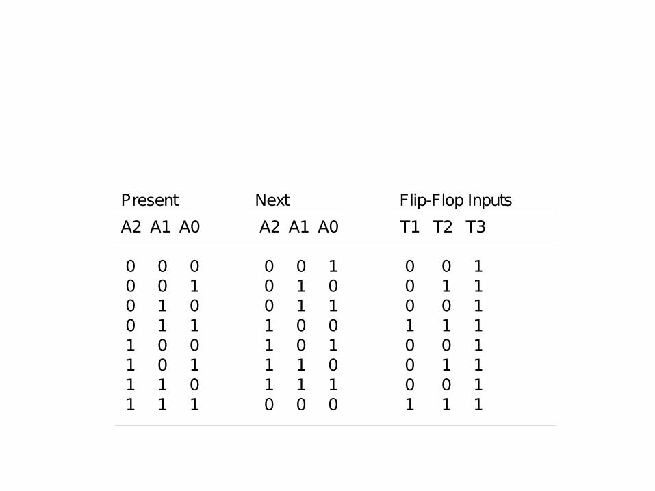
State Table for 3Bit Counter
Present Next Flip-Flop Inputs
A2 A1 A0
0 0 0 0 0 1 0 1 0 0 1 1 1 0 0 1 0 1 1 1 0 1 1 1
A2 A1 A0
0 0 1 0 1 0 0 1 1 1 0 0 1 0 1 1 1 0 1 1 1 0 0 0
Present Next Flip-Flop Inputs
A2 A1 A0
0 0 0 0 0 1 0 1 0 0 1 1 1 0 0 1 0 1 1 1 0 1 1 1
A2 A1 A0
0 0 1 0 1 0 0 1 1 1 0 0 1 0 1 1 1 0 1 1 1 0 0 0
T1 T2 T3
0 0 1 0 1 1 0 0 1 1 1 1 0 0 1 0 1 1 0 0 1 1 1 1