Embed Size (px)
Citation preview
Asynchronous Sequential Logic
Chapter 9
Digital Circuits 2
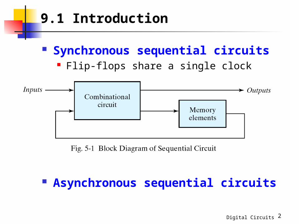
9.1 Introduction
Synchronous sequential circuits Flip-flops share a single clock
Asynchronous sequential circuits
Digital Circuits 3
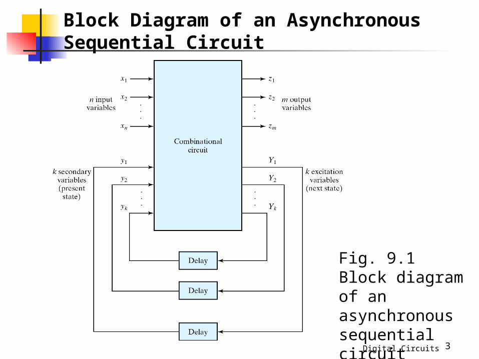
Fig. 9.1Block diagram of an asynchronous sequential circuit
Block Diagram of an Asynchronous Sequential Circuit
Digital Circuits 4
no clock pulse
Memory elements in asynchronous circuits are either unclocked flip-flops or time delay elements
In a gate-type circuit, the propagation delay that exists in the combinational circuit path from input to output provides sufficient delay along the feedback loop so that no specific delay elements are actually inserted in the feedback path
difficult to design: Timing problems involved in the feedback path
Asynchronous Sequential Circuit
Digital Circuits 5
must attain a stable state before the input is changed to a new value
Because of delays in the wires and the gates, it is impossible to have two or more input variables change at exactly the same instant of time without an uncertainty as to which one changes first.
Therefore, simultaneous changes of two or more variables are usually prohibited.
This restrictions means that only one input variable can change at any one time and the time between two input changes must be longer than the time it takes the circuit to reach a stable state.
Asynchronous Sequential Circuit
Digital Circuits 6
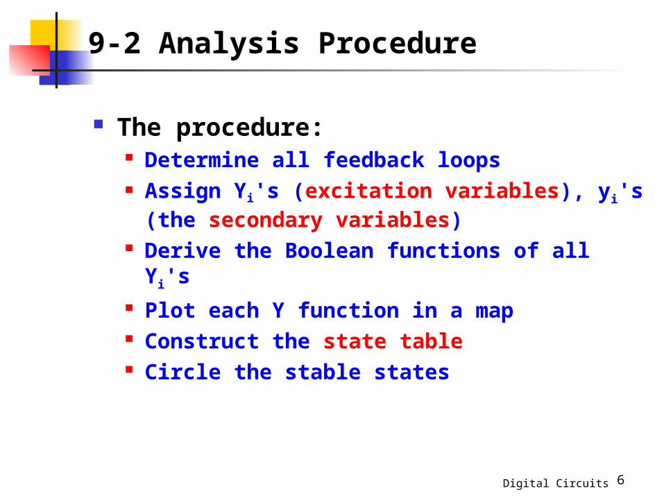
9-2 Analysis Procedure
The procedure: Determine all feedback loops Assign Yi's (excitation variables), yi's (the
secondary variables) Derive the Boolean functions of all Yi's Plot each Y function in a map Construct the state table Circle the stable states
Digital Circuits 7
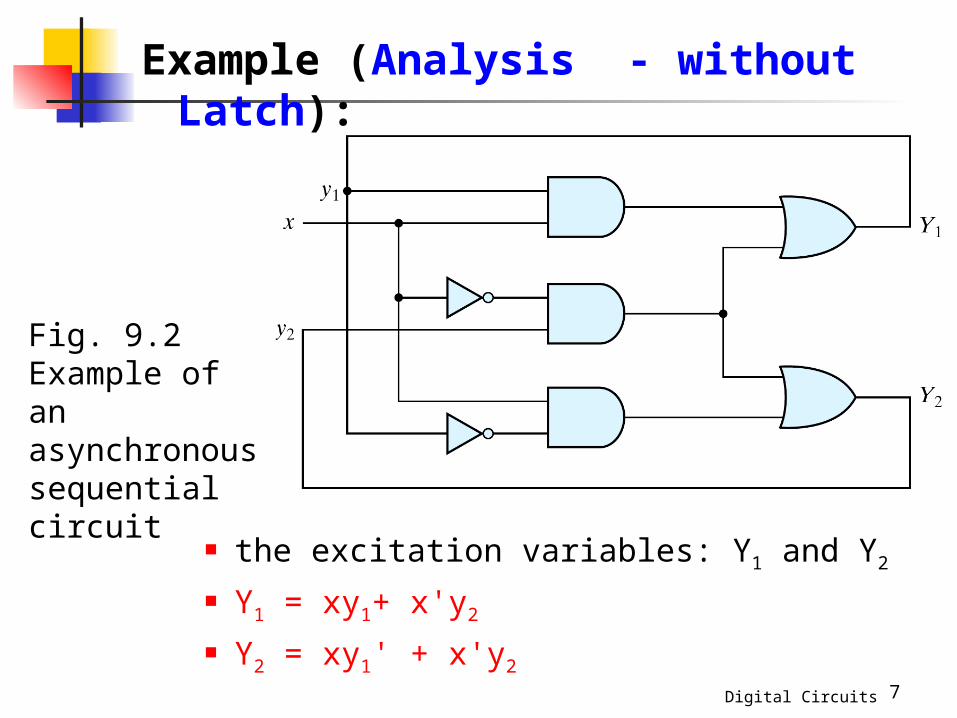
the excitation variables: Y1 and Y2
Y1 = xy1+ x'y2
Y2 = xy1' + x'y2
Fig. 9.2Example of an asynchronous sequential circuit
Example (Analysis - without Latch):
Digital Circuits 8
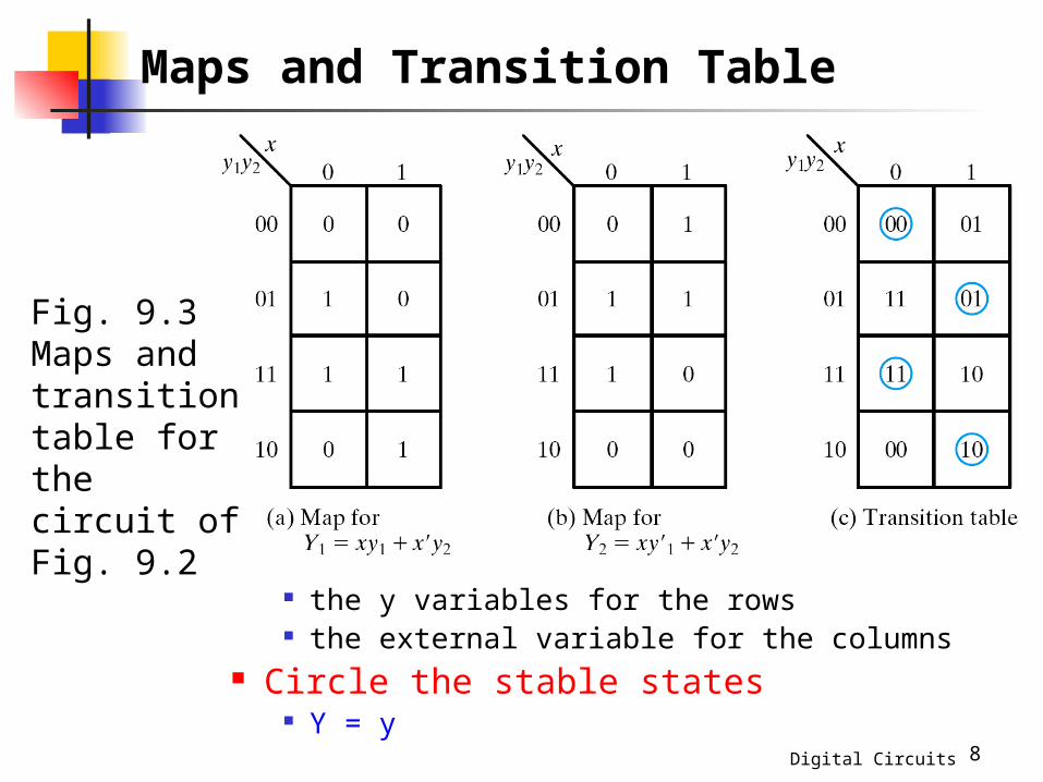
the y variables for the rows the external variable for the columns
Circle the stable states Y = y
Fig. 9.3Maps and transition table for the circuit of Fig. 9.2
Maps and Transition Table
Digital Circuits 9
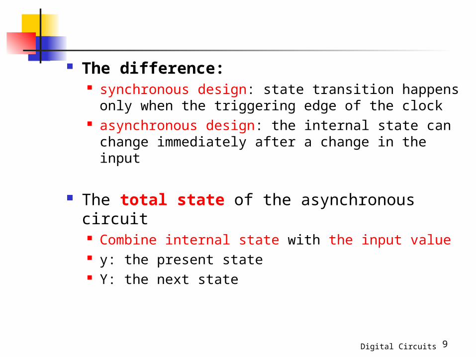
The difference: synchronous design: state transition happens only
when the triggering edge of the clock asynchronous design: the internal state can
change immediately after a change in the input
The total state of the asynchronous circuit Combine internal state with the input value y: the present state Y: the next state
Digital Circuits 10
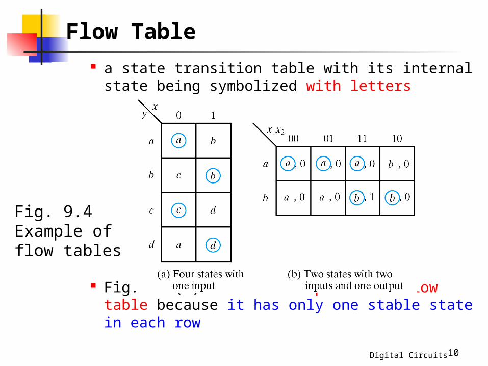
a state transition table with its internal state being symbolized with letters
Fig. 9-4(a) is called a primitive flow table because it has only one stable state in each row
Fig. 9.4Example of flow tables
Flow Table
Digital Circuits 11
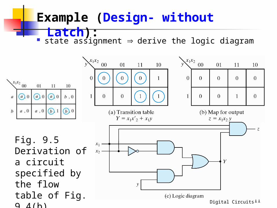
state assignment derive the logic diagram
Fig. 9.5Derivation of a circuit specified by the flow table of Fig. 9.4(b)
Example (Design- without Latch):
Digital Circuits 12
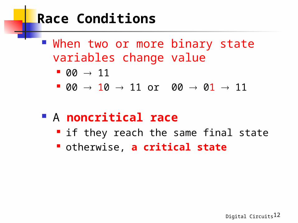
When two or more binary state variables change value 00 11 00 10 11 or 00 01 11
A noncritical race if they reach the same final state otherwise, a critical state
Race Conditions
Digital Circuits 13
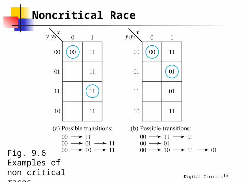
Fig. 9.6Examples of non-critical races
Noncritical Race
Digital Circuits 14
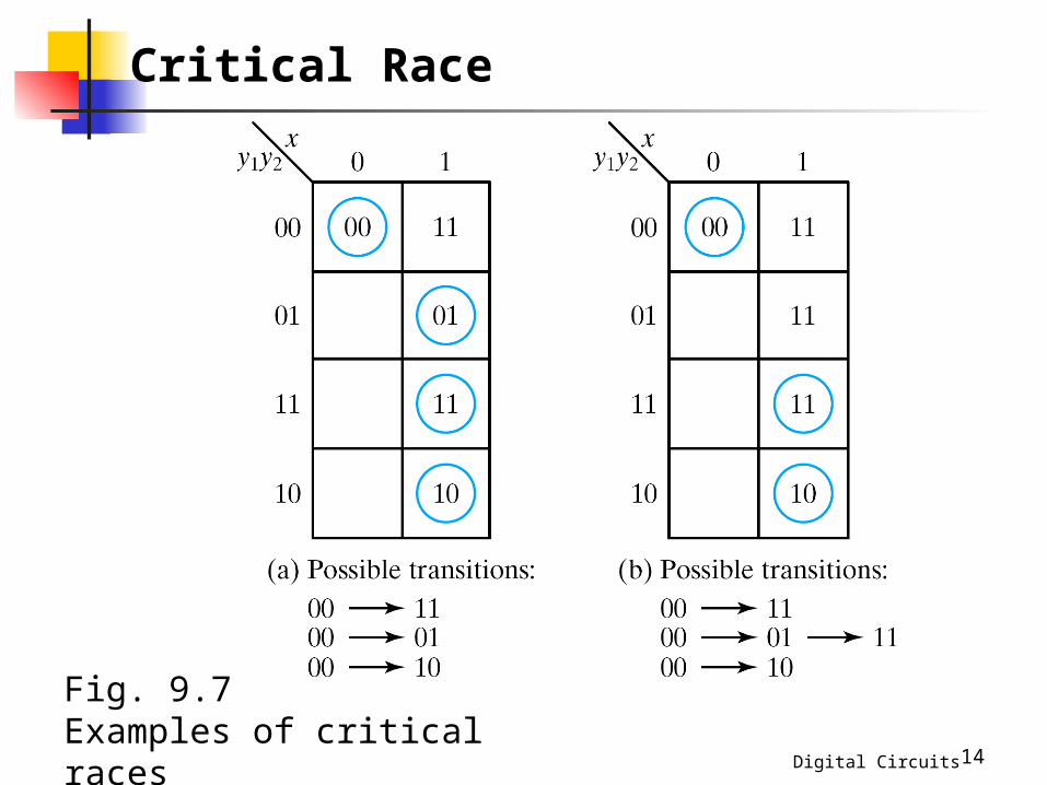
Fig. 9.7Examples of critical races
Critical Race
Digital Circuits 15
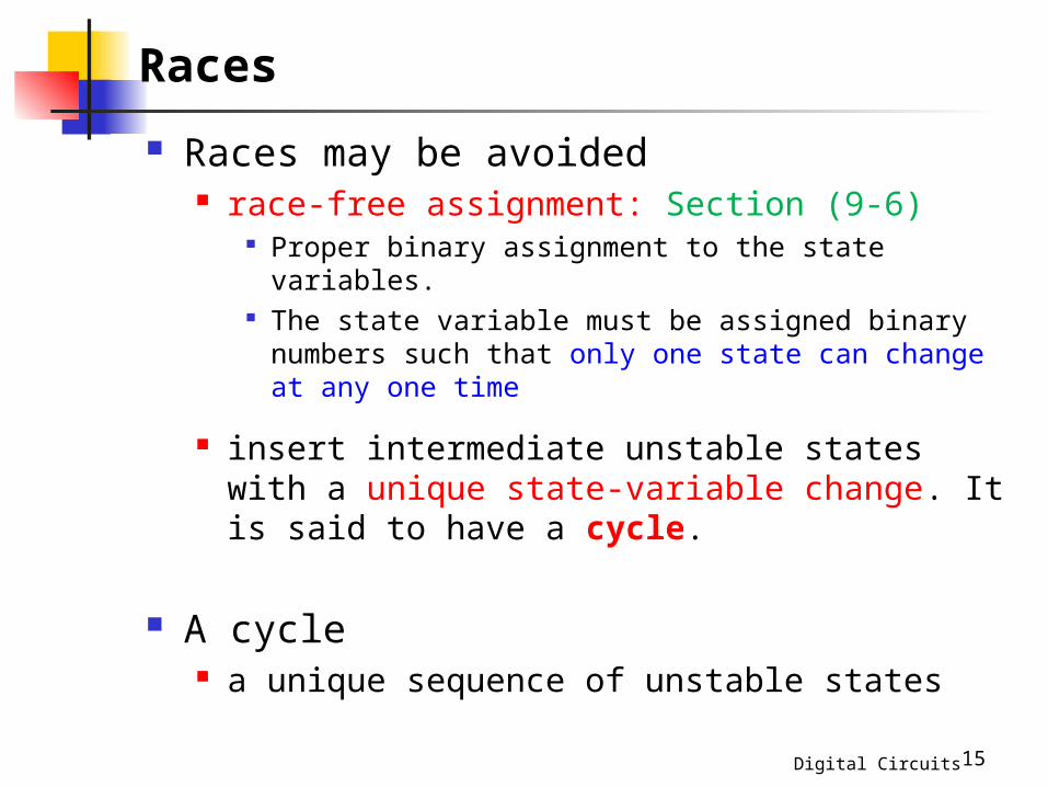
Races may be avoided race-free assignment: Section (9-6)
Proper binary assignment to the state variables. The state variable must be assigned binary numbers
such that only one state can change at any one time
insert intermediate unstable states with a unique state-variable change. It is said to have a cycle.
A cycle a unique sequence of unstable states
Races
Digital Circuits 16
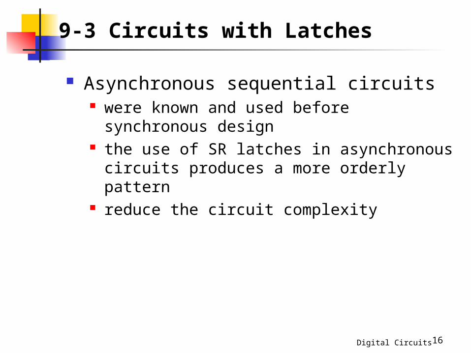
9-3 Circuits with Latches
Asynchronous sequential circuits were known and used before synchronous design the use of SR latches in asynchronous circuits
produces a more orderly pattern reduce the circuit complexity
Digital Circuits 17
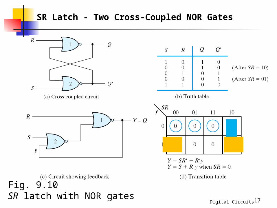
SR Latch - Two Cross-Coupled NOR Gates
Fig. 9.10SR latch with NOR gates
Digital Circuits 18
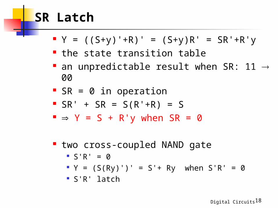
Y = ((S+y)'+R)' = (S+y)R' = SR'+R'y the state transition table an unpredictable result when SR: 11 00 SR = 0 in operation SR' + SR = S(R'+R) = S Y = S + R'y when SR = 0
two cross-coupled NAND gate S'R' = 0 Y = (S(Ry)')' = S'+ Ry when S'R' = 0 S'R' latch
SR Latch
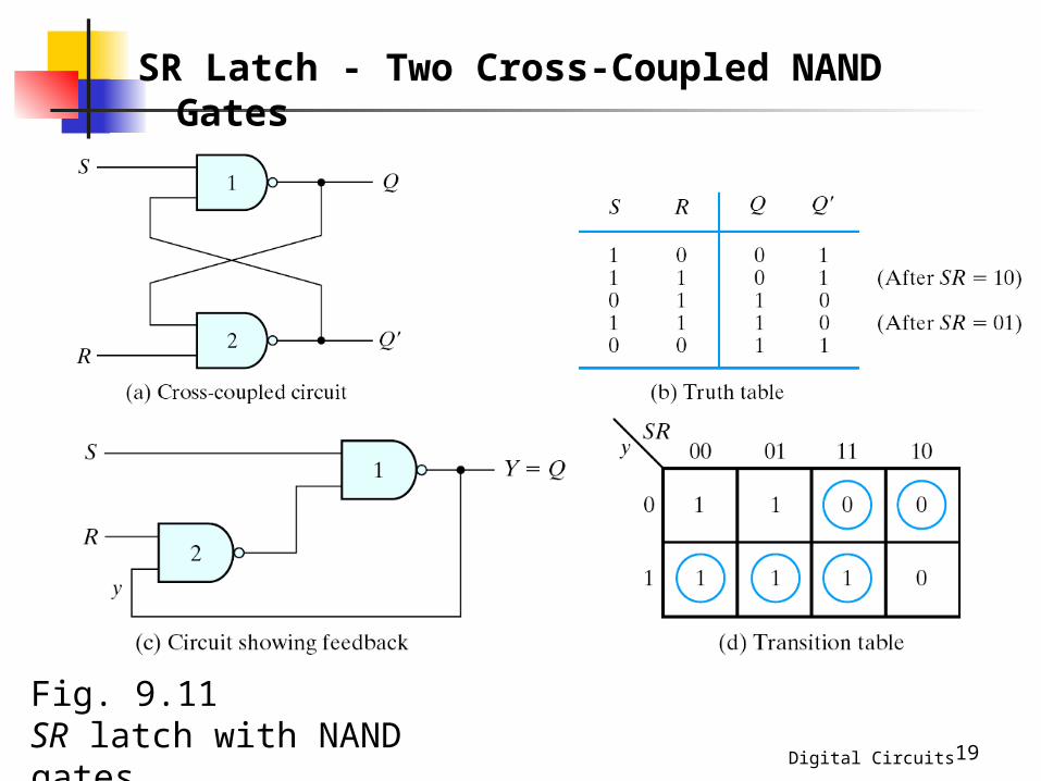
Digital Circuits 19
Fig. 9.11SR latch with NAND gates
SR Latch - Two Cross-Coupled NAND Gates

Digital Circuits 20
Example (Analysis - with Latch):
Fig. 9.12Examples of a circuit with SR latch
Digital Circuits 21
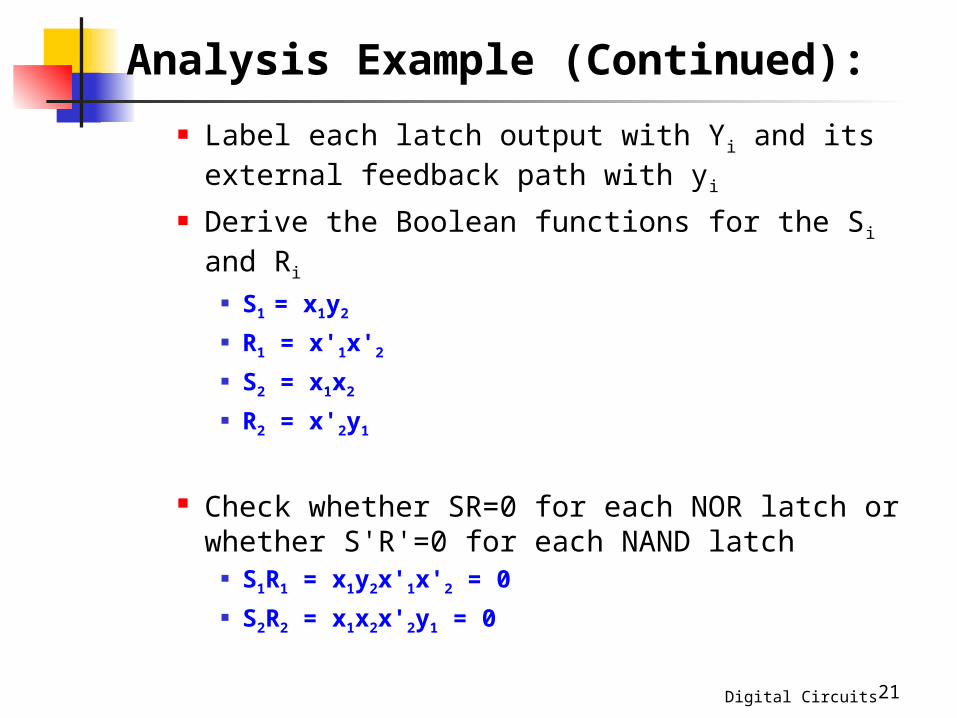
Label each latch output with Yi and its external feedback path with yi
Derive the Boolean functions for the Si and Ri
S1 = x1y2
R1 = x'1x'2 S2 = x1x2
R2 = x'2y1
Check whether SR=0 for each NOR latch or whether S'R'=0 for each NAND latch
S1R1 = x1y2x'1x'2 = 0
S2R2 = x1x2x'2y1 = 0
Analysis Example (Continued):
Digital Circuits 22
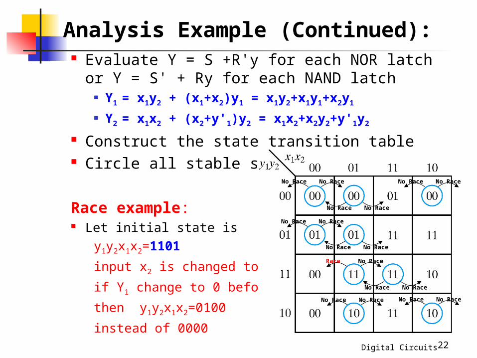
Evaluate Y = S +R'y for each NOR latch or Y = S' + Ry for each NAND latch
Y1 = x1y2 + (x1+x2)y1 = x1y2+x1y1+x2y1
Y2 = x1x2 + (x2+y'1)y2 = x1x2+x2y2+y'1y2
Construct the state transition table Circle all stable states
Race example: Let initial state is
y1y2x1x2=1101
input x2 is changed to 0
if Y1 change to 0 before Y2
then y1y2x1x2=0100
instead of 0000
Analysis Example (Continued):
No Race
No Race
No Race
No Race
No Race
No Race
No Race
No Race
No Race
No Race
No Race
Race
No Race
No Race
No Race
No Race
No Race
No Race
Digital Circuits 23
Analysis Procedure
Digital Circuits 24
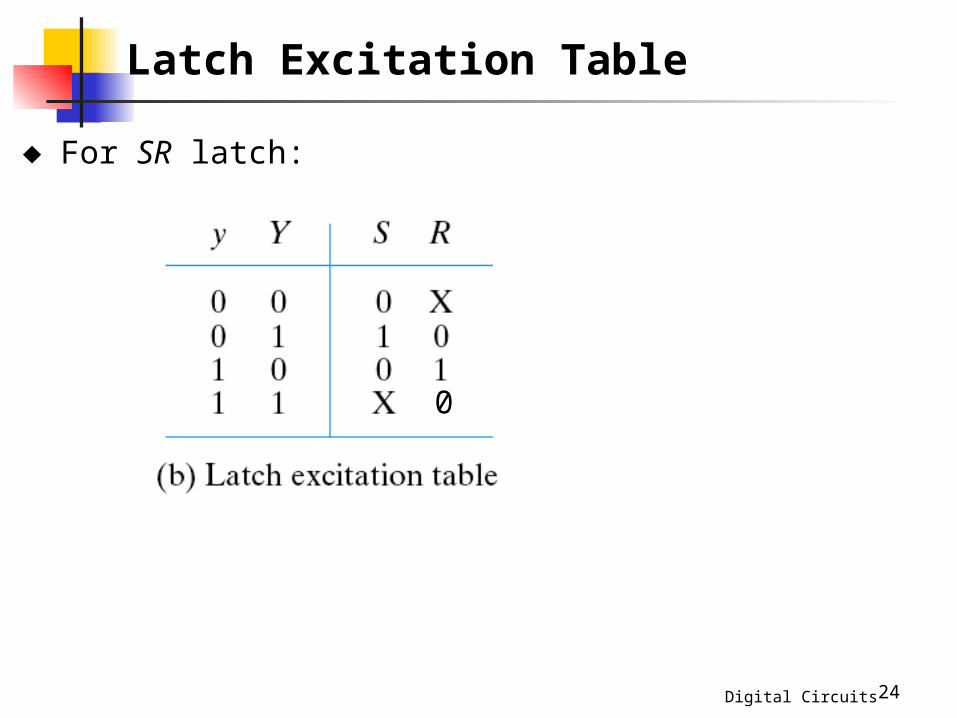
Latch Excitation Table
For SR latch:
0
Digital Circuits 25
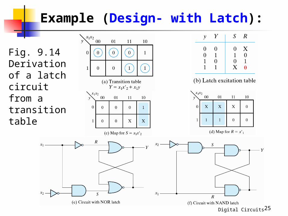
Fig. 9.14Derivation of a latch circuit from a transition table
Example (Design- with Latch):
Digital Circuits 26
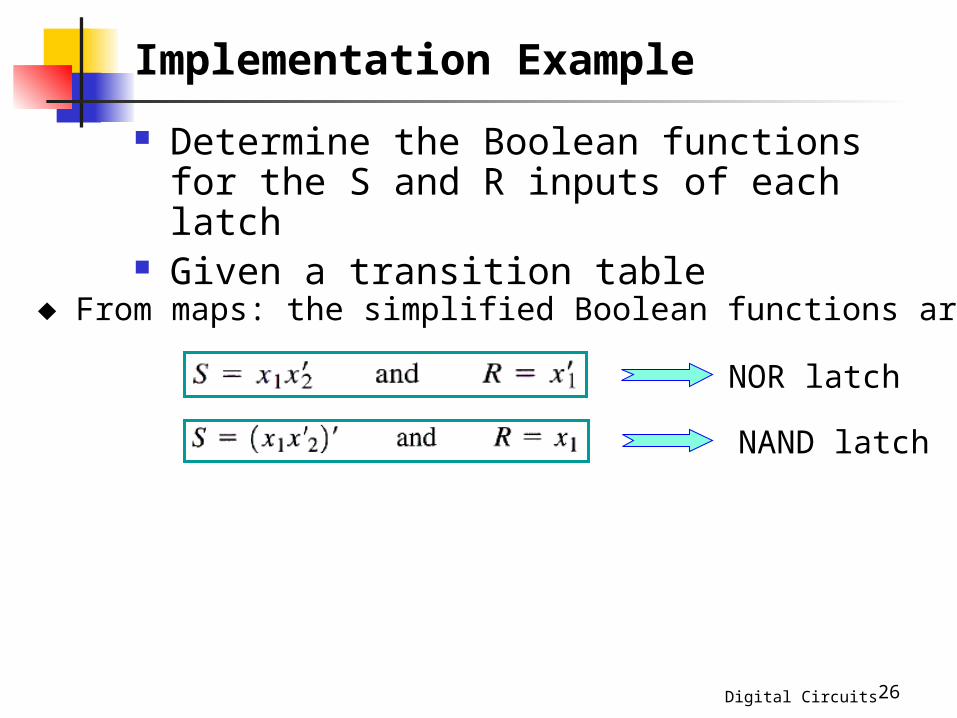
Determine the Boolean functions for the S and R inputs of each latch
Given a transition table
From maps: the simplified Boolean functions are
NOR latch
NAND latch
Implementation Example
Digital Circuits 27
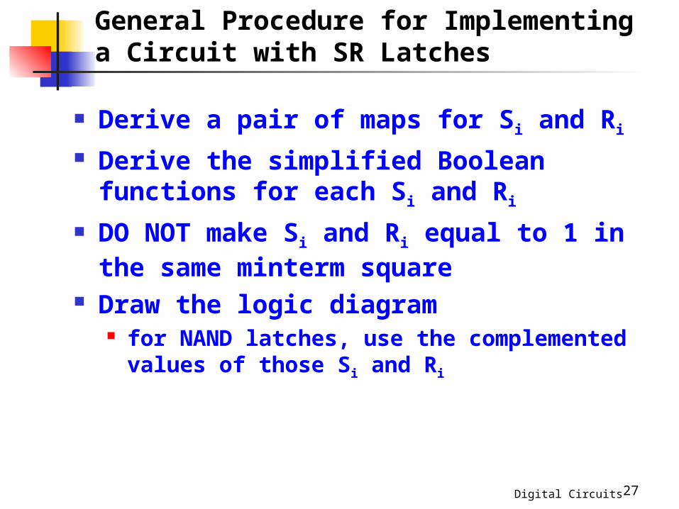
Derive a pair of maps for Si and Ri
Derive the simplified Boolean functions for each Si and Ri
DO NOT make Si and Ri equal to 1 in the same minterm square
Draw the logic diagram for NAND latches, use the complemented
values of those Si and Ri
General Procedure for Implementing a Circuit with SR Latches
Digital Circuits 28
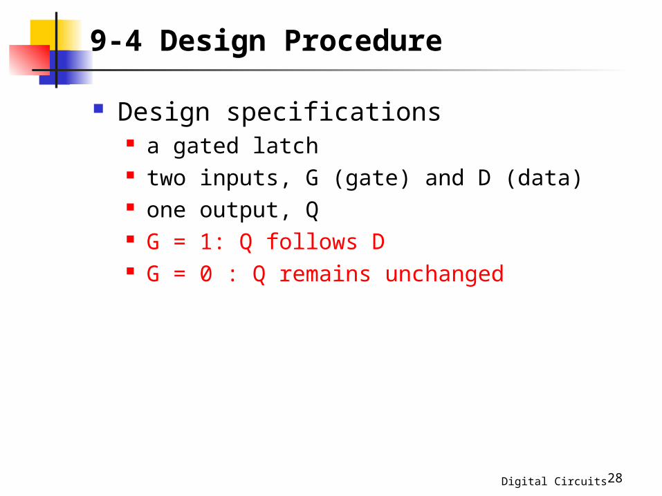
9-4 Design Procedure
Design specifications a gated latch two inputs, G (gate) and D (data) one output, Q G = 1: Q follows D G = 0 : Q remains unchanged
Digital Circuits 29
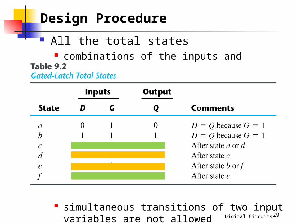
All the total states combinations of the inputs and internal states
simultaneous transitions of two input variables are not allowed
Design Procedure
Digital Circuits 30
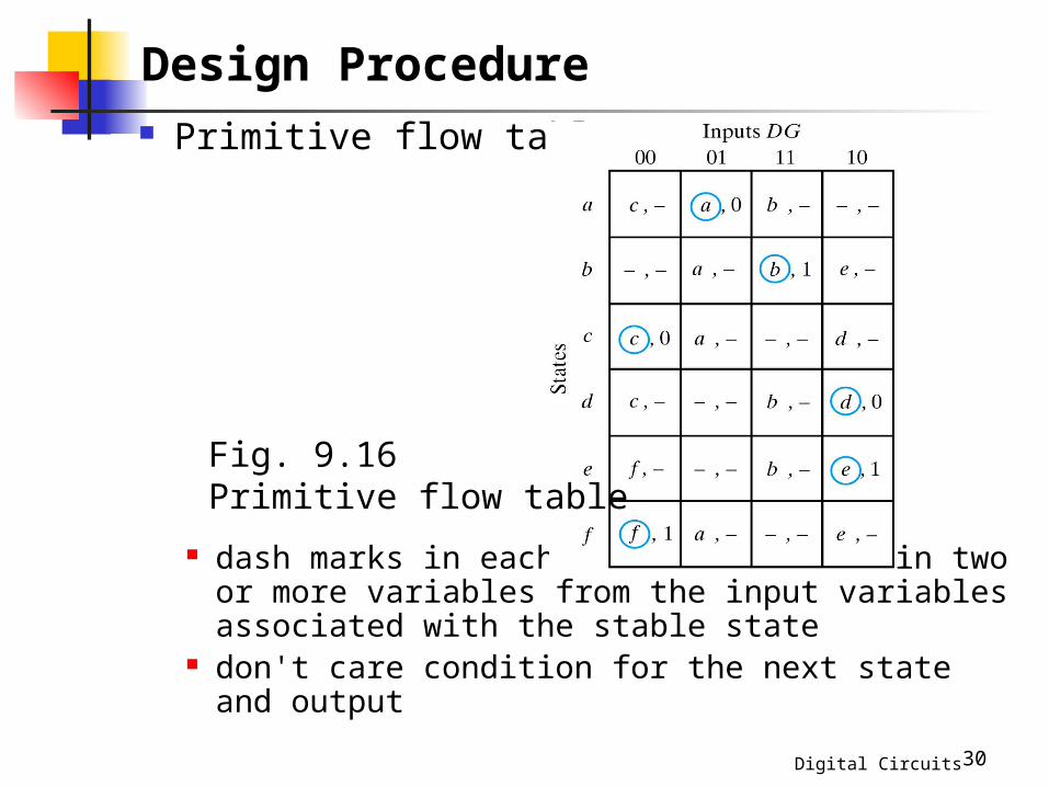
Primitive flow table
dash marks in each row that differs in two or more variables from the input variables associated with the stable state
don't care condition for the next state and output
Fig. 9.16Primitive flow table
Design Procedure
Digital Circuits 31
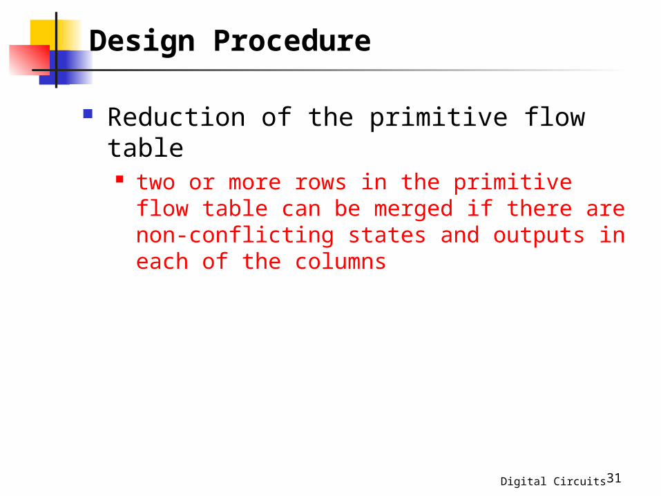
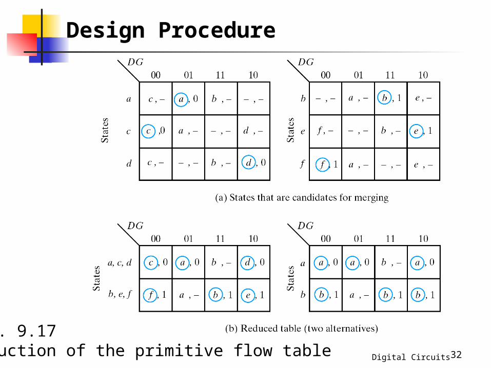
Reduction of the primitive flow table two or more rows in the primitive flow table can be
merged if there are non-conflicting states and outputs in each of the columns
Design Procedure
Digital Circuits 32
Fig. 9.17Reduction of the primitive flow table
Design Procedure
Digital Circuits 33
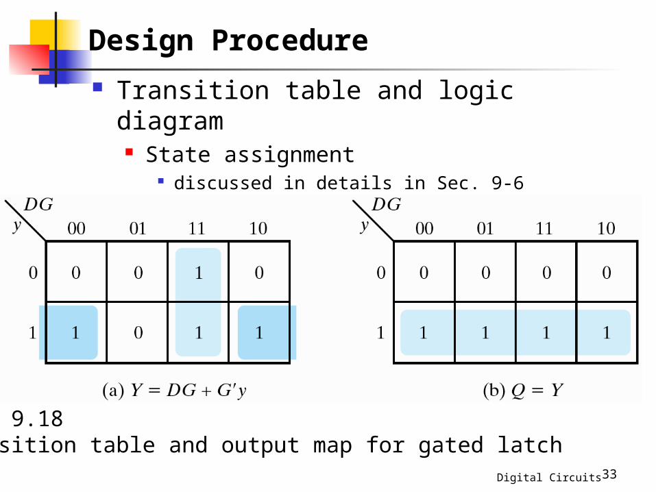
Transition table and logic diagram State assignment
discussed in details in Sec. 9-6 a:0, b:1
Fig. 9.18Transition table and output map for gated latch
Design Procedure
Digital Circuits 34
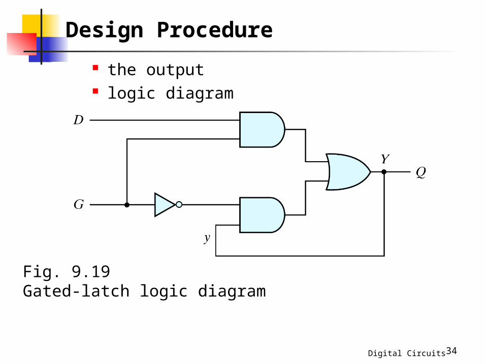
the output logic diagram
Fig. 9.19Gated-latch logic diagram
Design Procedure
Digital Circuits 35
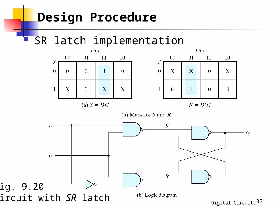
Fig. 9.20Circuit with SR latch
Design Procedure
SR latch implementation
Digital Circuits 36
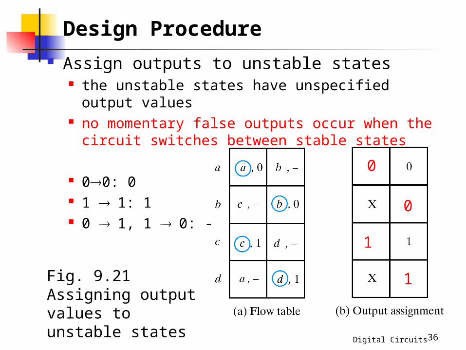
Fig. 9.21Assigning output values to unstable states
Design Procedure Assign outputs to unstable states
the unstable states have unspecified output values no momentary false outputs occur when the circuit
switches between stable states
00: 0 1 1: 1 0 1, 1 0: -
0
0
1
1
Digital Circuits 37
The procedure for making the assignment to outputs associated with unstable states can be summarized follows:
Design Procedure