Embed Size (px)
Citation preview

INF4420 Spring 2013 Analog to Digital Converters Jørgen Andreas Michaelsen ([email protected])
INF4420
Analog to Digital Converters
Jørgen Andreas Michaelsen
Spring 2013
1 / 34
Spring 2013 Analog to Digital Converters 2
Outline
Overview of architectures for implementing analog to digital conversion
2 / 34

INF4420 Spring 2013 Analog to Digital Converters Jørgen Andreas Michaelsen ([email protected])
Introduction
ADCs are used in numerous applications with differing requirements on speed, accuracy, and energy efficiency.
ADC architectures have different strengths and weaknesses with respect to these trade offs. It is therefore important to understand not only how each converter works, but also its limitations and key aspects for performance.
Spring 2013 Analog to Digital Converters 3
3 / 34
Numerous architectures
• Flash
• Interpolating
• Folding
• Interleaved
• Successive approximation
• Algorithmic
• Pipelined
• Two-step
• Integrating
Spring 2013 Analog to Digital Converters 4
4 / 34
INF4420 Spring 2013 Analog to Digital Converters Jørgen Andreas Michaelsen ([email protected])
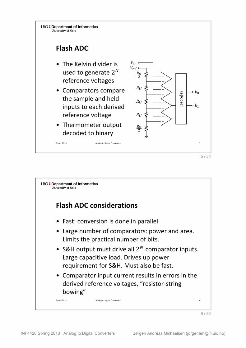
Flash ADC
• The Kelvin divider is used to generate 2𝑁 reference voltages
• Comparators compare the sample and held inputs to each derived reference voltage
• Thermometer output decoded to binary
Spring 2013 Analog to Digital Converters 5
5 / 34
Flash ADC considerations
• Fast: conversion is done in parallel
• Large number of comparators: power and area. Limits the practical number of bits.
• S&H output must drive all 2𝑁 comparator inputs. Large capacitive load. Drives up power requirement for S&H. Must also be fast.
• Comparator input current results in errors in the derived reference voltages, “resistor-string bowing”
Spring 2013 Analog to Digital Converters 6
6 / 34

INF4420 Spring 2013 Analog to Digital Converters Jørgen Andreas Michaelsen ([email protected])
Flash ADC considerations
• Substrate and power supply noise: shielded (differential) clocks and separate analog supply to the comparator preamp. Bypass capacitors.
• Comparator errors such as metastability, noise, crosstalk, bandwidth, etc. cause “bubbles” in the thermometer code near the transition point. Thermometer decoder must take this into account.
• Comparator kickback noise.
Spring 2013 Analog to Digital Converters 7
7 / 34
Interpolating ADC
Similar to the flash ADC but comparator preamps are shared, and less derived reference voltages are needed. Less loading on the input.
Latches will see different delays. Can be compensated by adding resistance to laches close to the preamp.
Spring 2013 Analog to Digital Converters 8
8 / 34

INF4420 Spring 2013 Analog to Digital Converters Jørgen Andreas Michaelsen ([email protected])
Folding ADC
Preprocess the input to compress the signal range and decide the MSBs. Often used with interpolating ADCs.
Difficult to implement the folding circuit.
Spring 2013 Analog to Digital Converters 9
9 / 34
Time-interleaved ADC
• Flash converters are fast (conversion in parallel)
• Still, there is a limit to how fast we can make the comparators
• Techniques considered so far have focused on how we can reduce hardware complexity (avoiding 2𝑁 full comparators)
• We can make ADCs even faster by running multiple flash ADCs in parallel—time interleaved
Spring 2013 Analog to Digital Converters 10
10 / 34

INF4420 Spring 2013 Analog to Digital Converters Jørgen Andreas Michaelsen ([email protected])
Time-interleaved ADC
Example:
Monolithic
40 Gs/s
ADC in an
SiGe
process
Spring 2013 Analog to Digital Converters 11
http://www.lecroy.com/tm/Library/WhitePapers/PDF/DBI_Explained.pdf
11 / 34
Time-interleaved ADC
Technique to increase the sampling rate by interleaving.
Run 𝑁 ADCs in parallel. Requires fast S/H
Offset and gain mismatch between channels and clock misalignment
Spring 2013 Analog to Digital Converters 12
12 / 34

INF4420 Spring 2013 Analog to Digital Converters Jørgen Andreas Michaelsen ([email protected])
Time-interleaved ADC
Digital correction of gain and offset
Spring 2013 Analog to Digital Converters 13
13 / 34
Two-step ADC
A system of two ADCs and one DAC. First ADC resolves the MSBs, 𝑀 bits, and the second ADC resolves the LSBs, 𝑁 bits. 2𝑁 + 2𝑀 comparators (if flash is used), rather than 2𝑁+𝑀.
The MSB ADC must be accurate to 𝑀 +𝑁 bits. Spring 2013 Analog to Digital Converters 14
14 / 34

INF4420 Spring 2013 Analog to Digital Converters Jørgen Andreas Michaelsen ([email protected])
Two-step ADC
The residue is multiplied by 16 to scale it to a more practical range for the LSB ADC.
Spring 2013 Analog to Digital Converters 15
15 / 34
Two-step ADC error correction
Relax the accuracy requirement for the MSB ADC by overlapping the ranges of the ADCs.
Spring 2013 Analog to Digital Converters 16
16 / 34

INF4420 Spring 2013 Analog to Digital Converters Jørgen Andreas Michaelsen ([email protected])
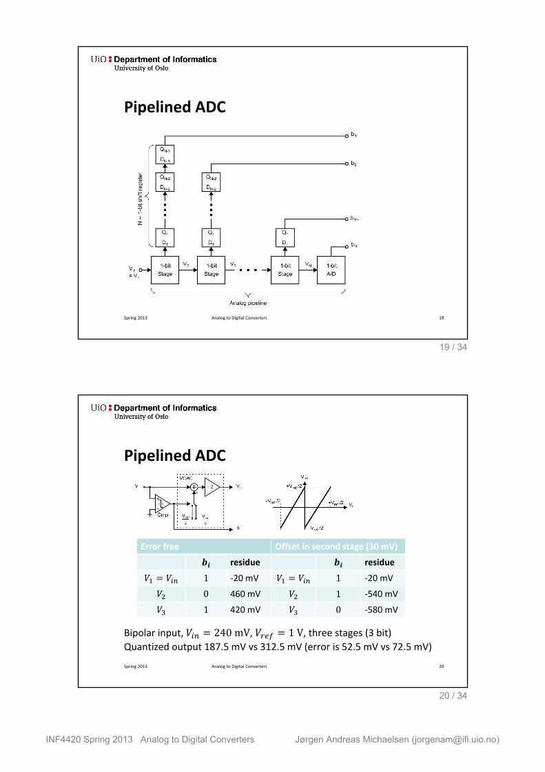
Pipelined ADC
Rather than using two ADC in sequence (two-step), we can use many.
Spring 2013 Analog to Digital Converters 17
unipolar
17 / 34
Pipelined ADC
Outputs a sample every clock cycle but the latency is 𝑁 (number of stages = number of bits assuming 1 bit per stage).
Spring 2013 Analog to Digital Converters 18
18 / 34
INF4420 Spring 2013 Analog to Digital Converters Jørgen Andreas Michaelsen ([email protected])
Pipelined ADC
Spring 2013 Analog to Digital Converters 19
19 / 34
Pipelined ADC
Bipolar input, 𝑉𝑖𝑛 = 240 mV, 𝑉𝑟𝑒𝑓 = 1 V, three stages (3 bit)
Quantized output 187.5 mV vs 312.5 mV (error is 52.5 mV vs 72.5 mV)
Spring 2013 Analog to Digital Converters 20
Error free Offset in second stage (30 mV)
𝒃𝒊 residue 𝒃𝒊 residue
𝑉1 = 𝑉𝑖𝑛 1 -20 mV 𝑉1 = 𝑉𝑖𝑛 1 -20 mV
𝑉2 0 460 mV 𝑉2 1 -540 mV
𝑉3 1 420 mV 𝑉3 0 -580 mV
20 / 34
INF4420 Spring 2013 Analog to Digital Converters Jørgen Andreas Michaelsen ([email protected])
Pipelined ADC
The signal is gained up by each stage → First stage must be the most accurate. Accuracy requirement relaxed by × 2 (input referred)
We can relax the offset accuracy requirements by adding redundancy, two comparators per stage, 1.5 bit, rather than one. Need more logic to decode the output value
Spring 2013 Analog to Digital Converters 21
21 / 34
Pipelined ADC
1.5 bit gives three possible output values from the
DAC, −𝑉𝑟𝑒𝑓
4, 0,𝑉𝑟𝑒𝑓
4, rather than −
𝑉𝑟𝑒𝑓
4,𝑉𝑟𝑒𝑓
4.
The two LSBs are determined by a 2 bit ADC. The final equivalent quantized input voltage is
𝑉𝑖𝑛 =𝑉𝑟𝑒𝑓
2 (𝑏𝑖,1+𝑏𝑖,0 − 1) ⋅ 2
−𝑖 + 𝐵𝑁−1,1 ⋅ 2𝑁−2
𝑁−2
𝑖=1
+ 𝐵𝑁−1,0 ⋅ 2𝑁−1
Decoder must do this addition
Spring 2013 Analog to Digital Converters 22
22 / 34
INF4420 Spring 2013 Analog to Digital Converters Jørgen Andreas Michaelsen ([email protected])
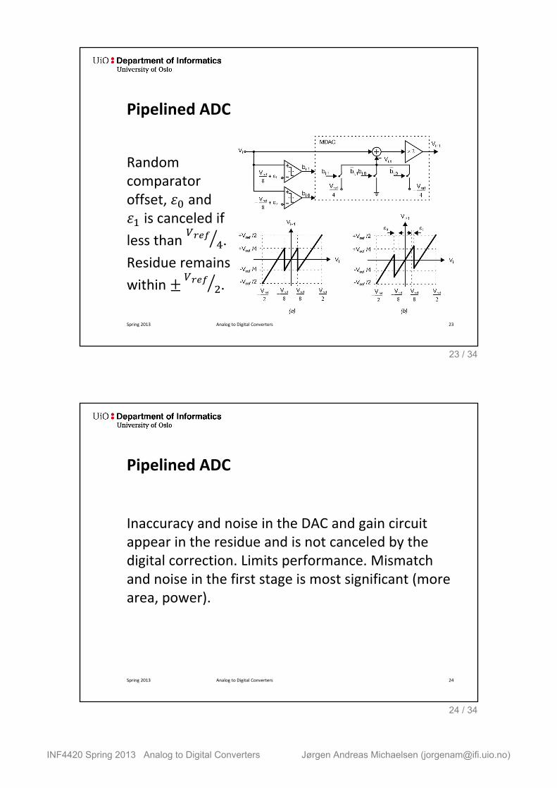
Pipelined ADC
Random comparator offset, 𝜀0 and 𝜀1 is canceled if
less than 𝑉𝑟𝑒𝑓
4 .
Residue remains
within ±𝑉𝑟𝑒𝑓
2 .
Spring 2013 Analog to Digital Converters 23
23 / 34
Pipelined ADC
Inaccuracy and noise in the DAC and gain circuit appear in the residue and is not canceled by the digital correction. Limits performance. Mismatch and noise in the first stage is most significant (more area, power).
Spring 2013 Analog to Digital Converters 24
24 / 34

INF4420 Spring 2013 Analog to Digital Converters Jørgen Andreas Michaelsen ([email protected])
Pipelined ADC
Generally, we can have 𝑘 bit per stage. Two stages equivalent to a two-step ADC.
More bits per stage gives less latency
Spring 2013 Analog to Digital Converters 25
25 / 34
Algorithmic ADC
Instead of cascading multiple stages in hardware, like the pipelined ADC, the same stage can be reused. However, each conversion takes N clock cycles.
Spring 2013 Analog to Digital Converters 26
26 / 34

INF4420 Spring 2013 Analog to Digital Converters Jørgen Andreas Michaelsen ([email protected])
SAR ADC
The successive approximation register (SAR) tests each bit sequentially (MSB first, one clock period per bit), and decides whether too keep the bit or not based on the comparator's output.
Spring 2013 Analog to Digital Converters 27
27 / 34
SAR ADC
Loop through N bits in N clock cycles. Binary search for the digital word (quantized representation) that is the closest match to the input voltage.
MSB determined first.
Spring 2013 Analog to Digital Converters 28
28 / 34

INF4420 Spring 2013 Analog to Digital Converters Jørgen Andreas Michaelsen ([email protected])
Charge redistribution SAR ADC
SAR ADCs are the most energy efficient ADCs
(in terms of FoM).
Limited in resolution by capacitor matching (~ 10 bits).
1. Sample mode
2. Hold mode
3. Bit cycling
Spring 2013 Analog to Digital Converters 29
• Inherent S/H function. • Auto zero of the comparator
is optional
29 / 34
Charge redistribution SAR ADC
No amplifiers needed (except for the comparator preamp). Saves power.
Comparator and charging of the capacitive array determines power consumption.
Spring 2013 Analog to Digital Converters 30
30 / 34
INF4420 Spring 2013 Analog to Digital Converters Jørgen Andreas Michaelsen ([email protected])
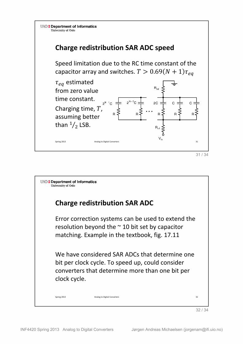
Charge redistribution SAR ADC speed
Speed limitation due to the RC time constant of the capacitor array and switches. 𝑇 > 0.69 𝑁 + 1 𝜏𝑒𝑞
𝜏𝑒𝑞 estimated
from zero value time constant.
Charging time, 𝑇, assuming better than 1 2 LSB.
Spring 2013 Analog to Digital Converters 31
31 / 34
Charge redistribution SAR ADC
Error correction systems can be used to extend the resolution beyond the ~ 10 bit set by capacitor matching. Example in the textbook, fig. 17.11
We have considered SAR ADCs that determine one bit per clock cycle. To speed up, could consider converters that determine more than one bit per clock cycle.
Spring 2013 Analog to Digital Converters 32
32 / 34

INF4420 Spring 2013 Analog to Digital Converters Jørgen Andreas Michaelsen ([email protected])
Integrating ADC
High accuracy, but low speed.
Phase I: Integrate 𝑉𝑖𝑛 for a fixed amount of time
Phase II: Measure the time it takes to discharge the integrator to zero with a fixed voltage
Spring 2013 Analog to Digital Converters 33
33 / 34
Integrating ADC
Phase I lasts for 𝑇1 = 2𝑁 ⋅ 𝑇𝑐𝑙𝑘, counter value when
phase II completes is the digital output.
Output word does not depend on 𝑅𝐶.
Spring 2013 Analog to Digital Converters 34
34 / 34