Embed Size (px)
Citation preview
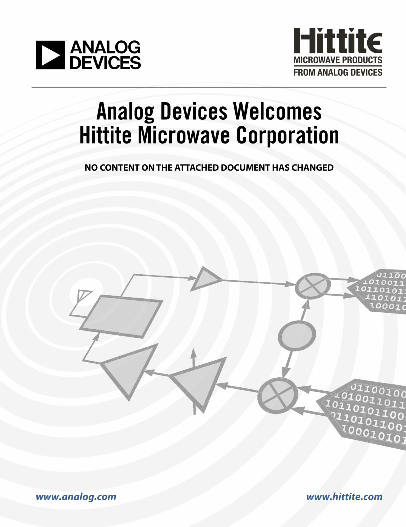
Analog Devices Welcomes Hittite Microwave Corporation
NO CONTENT ON THE ATTACHED DOCUMENT HAS CHANGED
www.analog.com www.hittite.com
HMC834* Product Page Quick LinksLast Content Update: 11/01/2016
Comparable PartsView a parametric search of comparable parts
Evaluation Kits• HMC834LP6GE Evaluation Board
DocumentationApplication Notes• Frequency Hopping with Hittite PLLVCOs Application
Note• PLL & PLLVCO Serial Programming Interface Mode
Selection Application Note• Power-Up & Brown-Out Design Considerations for RF
PLL+VCO Products Application Note• Wideband RF PLL+VCO and Clock Generation Products
FAQsData Sheet• HMC834 Data Sheet
Tools and Simulations• ADIsimPLL™
Reference MaterialsQuality Documentation• HMC Legacy PCN: LP6CE and LP6GE QFN - Alternate
assembly sourceTechnical Articles• Low Cost PLL with Integrated VCO Enables Compact LO
Solutions
Design Resources• HMC834 Material Declaration• PCN-PDN Information• Quality And Reliability• Symbols and Footprints
DiscussionsView all HMC834 EngineerZone Discussions
Sample and BuyVisit the product page to see pricing options
Technical SupportSubmit a technical question or find your regional support number
* This page was dynamically generated by Analog Devices, Inc. and inserted into this data sheet. Note: Dynamic changes to the content on this page does not constitute a change to the revision number of the product data sheet. This content may be frequently modified.

THIS PAGE INTENTIONALLY LEFT BLANK
For price, delivery and to place orders: Hittite Microwave Corporation, 2 Elizabeth Drive, Chelmsford, MA 01824Phone: 978-250-3343 Fax: 978-250-3373 Order On-line at www.hittite.com
Application Support: Phone: 978-250-3343 or [email protected]
PLL
s w
ith
int
eg
rat
ed
VC
O -
sM
t
1
HMC834LP6GEv01.0112
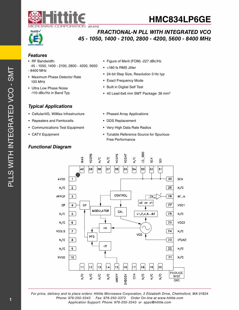
Fractional-n Pll with integrated Vco45 - 1050, 1400 - 2100, 2800 - 4200, 5600 - 8400 Mhz
Functional diagram
Features• rF Bandwidth: 45 - 1050, 1400 - 2100, 2800 - 4200, 5600 - 8400 Mhz
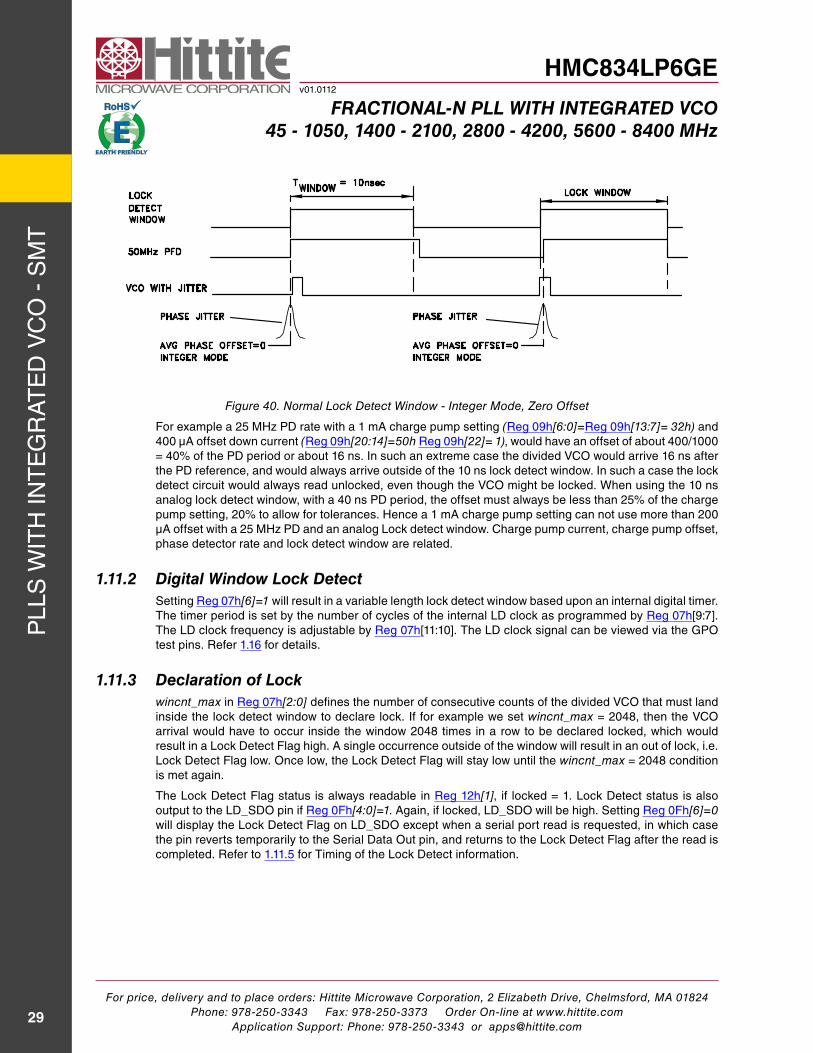
• Maximum Phase detector rate 100 Mhz
• Ultra Low Phase noise -110 dBc/hz in Band typ.
• Figure of Merit (FOM) -227 dBc/hz
• <180 fs rMs Jitter
• 24-bit step size, resolution 3 hz typ
• exact Frequency Mode
• Built in digital self test
• 40 Lead 6x6 mm sMt Package: 36 mm2
typical applications
• Cellular/4g, wiMax infrastructure
• repeaters and Femtocells
• Communications test equipment
• CatV equipment
• Phased array applications
• dds replacement
• Very high data rate radios
• tunable reference source for spurious- Free Performance
For price, delivery and to place orders: Hittite Microwave Corporation, 2 Elizabeth Drive, Chelmsford, MA 01824Phone: 978-250-3343 Fax: 978-250-3373 Order On-line at www.hittite.com
Application Support: Phone: 978-250-3343 or [email protected]
PLL
s w
ith
int
eg
rat
ed
VC
O -
sM
t
2
HMC834LP6GEv01.0112
Fractional-n Pll with integrated Vco45 - 1050, 1400 - 2100, 2800 - 4200, 5600 - 8400 Mhz
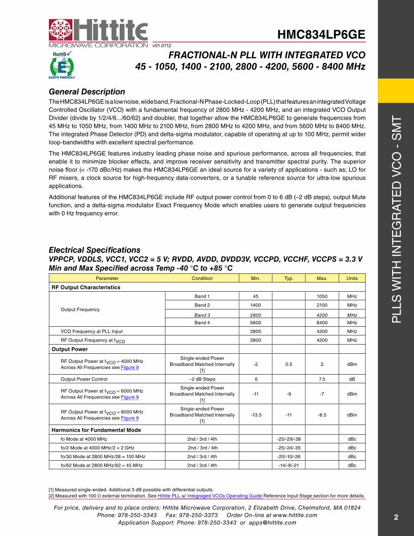
general descriptionthe hMC834LP6ge is a low noise, wide band, Fractional-n Phase-Locked-Loop (PLL) that features an integrated Voltage Controlled Oscillator (VCO) with a fundamental frequency of 2800 Mhz - 4200 Mhz, and an integrated VCO Output divider (divide by 1/2/4/6.../60/62) and doubler, that together allow the hMC834LP6ge to generate frequencies from 45 Mhz to 1050 Mhz, from 1400 Mhz to 2100 Mhz, from 2800 Mhz to 4200 Mhz, and from 5600 Mhz to 8400 Mhz. the integrated Phase detector (Pd) and delta-sigma modulator, capable of operating at up to 100 Mhz, permit wider loop-bandwidths with excellent spectral performance.
the hMC834LP6ge features industry leading phase noise and spurious performance, across all frequencies, that enable it to minimize blocker effects, and improve receiver sensitivity and transmitter spectral purity. the superior noise floor (< -170 dBc/hz) makes the hMC834LP6ge an ideal source for a variety of applications - such as; LO for rF mixers, a clock source for high-frequency data-converters, or a tunable reference source for ultra-low spurious applications.
additional features of the hMC834LP6ge include rF output power control from 0 to 6 dB (~2 dB steps), output Mute function, and a delta-sigma modulator exact Frequency Mode which enables users to generate output frequencies with 0 hz frequency error.
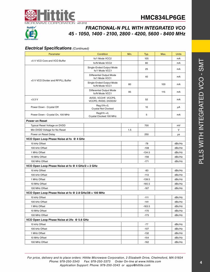
Parameter Condition Min. typ. Max. Units
RF Output Characteristics
Output Frequency
Band 1 45 1050 Mhz
Band 2 1400 2100 Mhz
Band 3 2800 4200 MHz
Band 4 5600 8400 Mhz
VCO Frequency at PLL input 2800 4200 Mhz
rF Output Frequency at fVCO 2800 4200 Mhz
Output Power
rF Output Power at fVCO = 4000 Mhz across all Frequencies see Figure 9
single-ended Power Broadband Matched internally
[1]-2 0.5 2 dBm
Output Power Control ~2 dB steps 6 7.5 dB
rF Output Power at fVCO = 6000 Mhz across all Frequencies see Figure 9
single-ended Power Broadband Matched internally
[1]-11 -9 -7 dBm
rF Output Power at fVCO = 8000 Mhz across all Frequencies see Figure 9
single-ended Power Broadband Matched internally
[1] -13.5 -11 -8.5 dBm
Harmonics for Fundamental Mode
fo Mode at 4000 Mhz 2nd / 3rd / 4th -25/-29/-38 dBc
fo/2 Mode at 4000 Mhz/2 = 2 ghz 2nd / 3rd / 4th -25/-24/-35 dBc
fo/30 Mode at 2800 Mhz/28 = 100 Mhz 2nd / 3rd / 4th -20/-10/-26 dBc
fo/62 Mode at 2800 Mhz/62 = 45 Mhz 2nd / 3rd / 4th -14/-8/-21 dBc
electrical SpecificationsVPPcP, VddlS, Vcc1, Vcc2 = 5 V; rVdd, aVdd, dVdd3V, VccPd, VcchF, VccPS = 3.3 V Min and Max Specified across temp -40 °c to +85 °c
[1] Measured single-ended. additional 3 dB possible with differential outputs.[2] Measured with 100 Ω external termination. see hittite PLL w/ integraged VCOs Operating guide reference input stage section for more details.
For price, delivery and to place orders: Hittite Microwave Corporation, 2 Elizabeth Drive, Chelmsford, MA 01824Phone: 978-250-3343 Fax: 978-250-3373 Order On-line at www.hittite.com
Application Support: Phone: 978-250-3343 or [email protected]
PLL
s w
ith
int
eg
rat
ed
VC
O -
sM
t
3
HMC834LP6GEv01.0112
Fractional-n Pll with integrated Vco45 - 1050, 1400 - 2100, 2800 - 4200, 5600 - 8400 Mhz
Parameter Condition Min. typ. Max. Units
Harmonics in Doubler Mode
2fo Mode at 5600 Mhz 1/2 / 3rd / 4th/5th -10/-22/-25/-35 dBc
VCO Output Divider
VCO rF divider range 1,2,4,6,8,...,62 1 62
PLL RF Divider Characteristics
19-Bit n-divider range (integer) Max = 219 - 1 16 524,287
19-Bit n-divider range (Fractional)Fractional nominal divide ratio
varies (-3 / +4) dynamically max20 524,283
REF Input Characteristics
Max ref input Frequency 350 Mhz
ref input VoltageaC Coupled
[2]1 2 3.3 Vp-p
ref input Capacitance 5 pF
14-Bit r-divider range 1 16,383
Phase Detector (PD) [3]
Pd Frequency Fractional Mode B [4] dC 100 Mhz
Pd Frequency Fractional Mode a (and register 6 [17:16] = 11)
dC 80 Mhz
Pd Frequency integer Mode dC 125 Mhz
Charge Pump
Output Current 0.02 2.54 ma
Charge Pump gain step size 20 µa
Pd/Charge Pump ssB Phase noise 50 Mhz ref, input referred
1 khz -143 dBc/hz
10 khz add 1 dB for Fractional -150 dBc/hz
100 khz add 3 dB for Fractional -153 dBc/hz
Logic Inputs
Vsw 40 50 60 % dVdd
Logic Outputs
VOh Output high Voltage dVdd V
VOL Output Low Voltage 0 V
Output impedance 100 200 Ω
Maximum Load Current 1.5 ma
Power Supply Voltages
3.3 V suppliesaVdd, VCChF, VCCPs,VCCPd, rVdd,dVdd
3.0 3.3 3.5 V
5 V supplies VPPCP, VddLs, VCC1, VCC2 4.8 5 5.2 V
Power Supply Currents
+5 V analog Charge Pump VPPCP, VddLs 8 ma
electrical Specifications (Continued)
[3] slew rate of greater or equal to 0.5 ns/V is recommended, see PLL with integrated rF VCOs Operating guide for more details. Frequency is guaranteed across process voltage and temperature from -40 °C to +85 °C.[4] this maximum phase detector frequency can only be achieved if the minimum n value is respected. eg. in the case of fractional feedback mode, the maximum PFd rate = fvco/20 or 100 Mhz, whichever is less.
For price, delivery and to place orders: Hittite Microwave Corporation, 2 Elizabeth Drive, Chelmsford, MA 01824Phone: 978-250-3343 Fax: 978-250-3373 Order On-line at www.hittite.com
Application Support: Phone: 978-250-3343 or [email protected]
PLL
s w
ith
int
eg
rat
ed
VC
O -
sM
t
4
HMC834LP6GEv01.0112
Fractional-n Pll with integrated Vco45 - 1050, 1400 - 2100, 2800 - 4200, 5600 - 8400 Mhz
electrical Specifications (Continued)
Parameter Condition Min. typ. Max. Units
+5 V VCO Core and VCO Bufferfo/1 Mode VCC2 105 ma
fo/n Mode VCC2 80 ma
+5 V VCO divider and rF/PLL Buffer
single-ended Output Mode fo/1 Mode VCC1
25 ma
differential Output Modefo/1 Mode VCC1
40 ma
single-ended Output Modefo/n Mode VCC1
80 100 ma
differential Output Modefo/n Mode VCC1
95 115 ma
+3.3 VaVdd, VCChF, VCCPs, VCCPd, rVdd, dVdd3V
52 ma
Power down - Crystal Offreg 01h=0,
Crystal not Clocked10 µa
Power down - Crystal On, 100 Mhzreg01h =0,
Crystal Clocked 100 Mhz5 ma
Power on Reset
typical reset Voltage on dVdd 700 mV
Min dVdd Voltage for no reset 1.5 V
Power on reset delay 250 µs
VCO Open Loop Phase Noise at fo @ 4 GHz
10 khz Offset -78 dBc/hz
100 khz Offset -108 dBc/hz
1 Mhz Offset -134.5 dBc/hz
10 Mhz Offset -156 dBc/hz
100 Mhz Offset -171 dBc/hz
VCO Open Loop Phase Noise at fo @ 4 GHz/2 = 2 GHz
10 khz Offset -83 dBc/hz
100 khz Offset -113 dBc/hz
1 Mhz Offset -139.5 dBc/hz
10 Mhz Offset -165.5 dBc/hz
100 Mhz Offset -167 dBc/hz
VCO Open Loop Phase Noise at fo @ 2.8 GHz/28 = 100 MHz
10 khz Offset -111 dBc/hz
100 khz Offset -141 dBc/hz
1 Mhz Offset -163.5 dBc/hz
10 Mhz Offset -170 dBc/hz
100 Mhz Offset -173 dBc/hz
VCO Open Loop Phase Noise at 2fo @ 5.6 GHz
10 khz Offset -77 dBc/hz
100 khz Offset -107 dBc/hz
1 Mhz Offset -132 dBc/hz
10 Mhz Offset -154 dBc/hz
100 Mhz Offset -162 dBc/hz
For price, delivery and to place orders: Hittite Microwave Corporation, 2 Elizabeth Drive, Chelmsford, MA 01824Phone: 978-250-3343 Fax: 978-250-3373 Order On-line at www.hittite.com
Application Support: Phone: 978-250-3343 or [email protected]
PLL
s w
ith
int
eg
rat
ed
VC
O -
sM
t
5
HMC834LP6GEv01.0112
Fractional-n Pll with integrated Vco45 - 1050, 1400 - 2100, 2800 - 4200, 5600 - 8400 Mhz
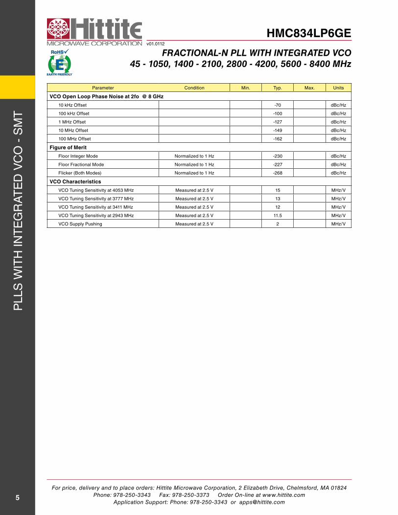
Parameter Condition Min. typ. Max. Units
VCO Open Loop Phase Noise at 2fo @ 8 GHz
10 khz Offset -70 dBc/hz
100 khz Offset -100 dBc/hz
1 Mhz Offset -127 dBc/hz
10 Mhz Offset -149 dBc/hz
100 Mhz Offset -162 dBc/hz
Figure of Merit
Floor integer Mode normalized to 1 hz -230 dBc/hz
Floor Fractional Mode normalized to 1 hz -227 dBc/hz
Flicker (Both Modes) normalized to 1 hz -268 dBc/hz
VCO Characteristics
VCO tuning sensitivity at 4053 Mhz Measured at 2.5 V 15 Mhz/V
VCO tuning sensitivity at 3777 Mhz Measured at 2.5 V 13 Mhz/V
VCO tuning sensitivity at 3411 Mhz Measured at 2.5 V 12 Mhz/V
VCO tuning sensitivity at 2943 Mhz Measured at 2.5 V 11.5 Mhz/V
VCO supply Pushing Measured at 2.5 V 2 Mhz/V
For price, delivery and to place orders: Hittite Microwave Corporation, 2 Elizabeth Drive, Chelmsford, MA 01824Phone: 978-250-3343 Fax: 978-250-3373 Order On-line at www.hittite.com
Application Support: Phone: 978-250-3343 or [email protected]
PLL
s w
ith
int
eg
rat
ed
VC
O -
sM
t
6
HMC834LP6GEv01.0112
Fractional-n Pll with integrated Vco45 - 1050, 1400 - 2100, 2800 - 4200, 5600 - 8400 Mhz
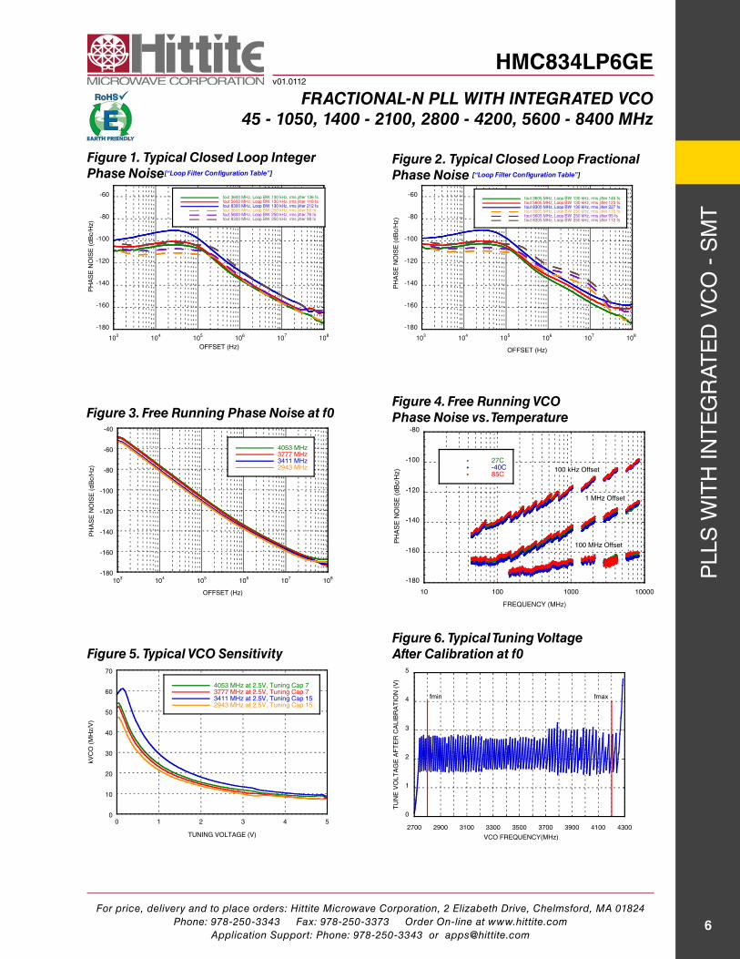
Figure 1. typical closed loop integer Phase noise[“loop Filter configuration table”]
Figure 5. typical Vco Sensitivity
-180
-160
-140
-120
-100
-80
-60
103
104
105
106
107
108
fout 3600 MHz, Loop BW 130 kHz, rms jitter 136 fsfout 5600 MHz, Loop BW 130 kHz, rms jitter 116 fsfout 8300 MHz, Loop BW 130 kHz, rms jitter 212 fsfout 3600 MHz, Loop BW 250 kHz, rms jitter 86 fsfout 5600 MHz, Loop BW 250 kHz, rms jitter 76 fsfout 8300 MHz, Loop BW 250 kHz, rms jitter 98 fs
PH
AS
E N
OIS
E (
dB
c/H
z)
OFFSET (Hz)
-180
-160
-140
-120
-100
-80
-60
-40
103
104
105
106
107
108
4053 MHz3777 MHz3411 MHz2943 MHz
OFFSET (Hz)
PH
AS
E N
OIS
E (
dB
c/H
z)
Figure 2. typical closed loop Fractional Phase noise [“loop Filter configuration table”]
Figure 3. Free running Phase noise at f0Figure 4. Free running Vco Phase noise vs. temperature
0
1
2
3
4
5
2700 2900 3100 3300 3500 3700 3900 4100 4300
TU
NE
VO
LT
AG
E A
FT
ER
CA
LIB
RA
TIO
N (
V)
VCO FREQUENCY(MHz)
fmin fmax
-180
-160
-140
-120
-100
-80
-60
103
104
105
106
107
108
fout 3605 MHz, Loop BW 130 kHz, rms jitter 145 fsfout 5605 MHz, Loop BW 130 kHz, rms jitter 123 fsfout 8305 MHz, Loop BW 130 kHz, rms jitter 227 fsfout 3605 MHz, Loop BW 250 kHz, rms jitter 110 fsfout 5605 MHz, Loop BW 250 kHz, rms jitter 95 fsfout 8305 MHz, Loop BW 250 kHz, rms jitter 112 fs
OFFSET (Hz)
PH
AS
E N
OIS
E (
dB
c/H
z)
0
10
20
30
40
50
60
70
0 1 2 3 4 5
4053 MHz at 2.5V, Tuning Cap 73777 MHz at 2.5V, Tuning Cap 73411 MHz at 2.5V, Tuning Cap 152943 MHz at 2.5V, Tuning Cap 15
TUNING VOLTAGE (V)
kV
CO
(M
Hz/V
)
Figure 6. typical tuning Voltage after calibration at f0
-180
-160
-140
-120
-100
-80
10 100 1000 10000
27C-40C85C
PH
AS
E N
OIS
E (
dB
c/H
z)
FREQUENCY (MHz)
100 MHz Offset
1 MHz Offset
100 kHz Offset
For price, delivery and to place orders: Hittite Microwave Corporation, 2 Elizabeth Drive, Chelmsford, MA 01824Phone: 978-250-3343 Fax: 978-250-3373 Order On-line at www.hittite.com
Application Support: Phone: 978-250-3343 or [email protected]
PLL
s w
ith
int
eg
rat
ed
VC
O -
sM
t
7
HMC834LP6GEv01.0112
Fractional-n Pll with integrated Vco45 - 1050, 1400 - 2100, 2800 - 4200, 5600 - 8400 Mhz
Figure 7. integrated rMS Jitter[1]
[1] rMs Jitter data is measured in fractional mode with 250 khz Loop bandwidth using 100 Mhz reference, Pd 50 Mhz. integration bandwidth from 1 khz to 100 Mhz.
[2] Measured from a 50 Ω source with a 100 Ω external resistor termination. see PLL with integrated rF VCOs Operating guide reference input stage section for more details. Full FOM performance up to maximum 3.3 Vpp input voltage.
[3] Measured from a 50 Ω source with a 100 Ω external resistor termination. see PLL with integrated rF VCOs Operating guide reference input stage section for more details. Full FOM performance up to maximum 3.3 Vpp input voltage.
40
60
80
100
120
140
160
180
200
10 100 1000 10000
-40C27C85C
RM
S J
ITT
ER
(fs
)
FREQUENCY (MHz)
-240
-230
-220
-210
-200
102
103
104
105
106
NO
RM
AL
IZE
D P
HA
SE
NO
ISE
(d
Bc/H
z)
FREQUENCY OFFSET (Hz)
FOM FloorFOM 1/f Noise
Typ FOM vs Offset
Figure 8. Figure of Merit
Figure 9. typical output Power vs. temperature, Maximum gain Figure 10. rF output return loss
-235
-230
-225
-220
-215
-15 -10 -5 0 5 10
14 MHz sq25 MHz sq50 MHz sq100 MHz sq
FL
OO
R F
OM
(d
Bc/H
z)
REFERENCE POWER (dBm)
100 MHz
14 MHz
50 MHz
25 MHz
Figure 12. reference input Sensitivity, Square wave, 50 Ω [2]
-15
-10
-5
0
5
10
0 1000 2000 3000 4000 5000 6000 7000 8000
27 C
-40 C85 C
OU
TP
UT
PO
WE
R (
dB
m)
OFFSET (MHz)
Figure 11. reference input Sensitivity Sinusoid wave, 50 Ω[3]
-235
-230
-225
-220
-215
-210
-205
-200
-20 -15 -10 -5 0 5
REFERENCE POWER (dBm)
FL
OO
R F
OM
(d
Bc/H
z)
14 MHz
25 MHz
50 MHz
100 MHz
-30
-25
-20
-15
-10
-5
0
100 1000 10000
FREQUENCY (MHz)
RE
TU
RN
LO
SS
(dB
)
For price, delivery and to place orders: Hittite Microwave Corporation, 2 Elizabeth Drive, Chelmsford, MA 01824Phone: 978-250-3343 Fax: 978-250-3373 Order On-line at www.hittite.com
Application Support: Phone: 978-250-3343 or [email protected]
PLL
s w
ith
int
eg
rat
ed
VC
O -
sM
t
8
HMC834LP6GEv01.0112
Fractional-n Pll with integrated Vco45 - 1050, 1400 - 2100, 2800 - 4200, 5600 - 8400 Mhz
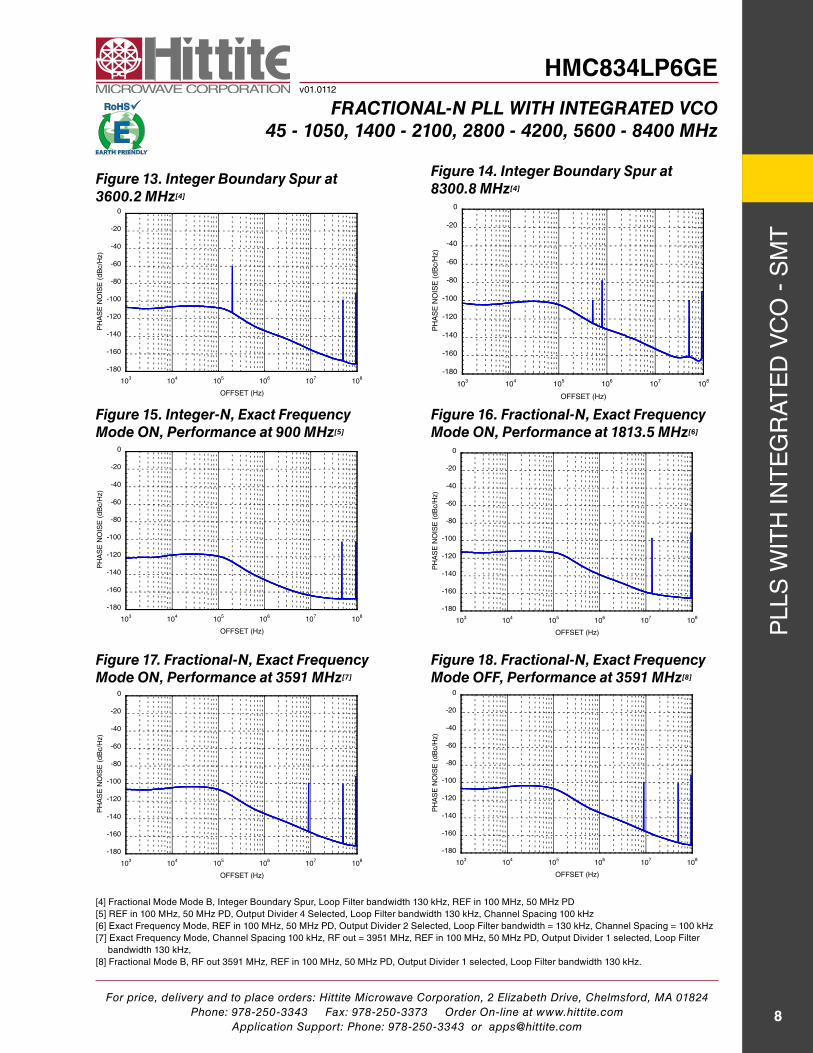
Figure 13. integer Boundary Spur at 3600.2 Mhz[4]
-180
-160
-140
-120
-100
-80
-60
-40
-20
0
103
104
105
106
107
108
PH
AS
E N
OIS
E (
dB
c/H
z)
OFFSET (Hz)
-180
-160
-140
-120
-100
-80
-60
-40
-20
0
103
104
105
106
107
108
PH
AS
E N
OIS
E (
dB
c/H
z)
OFFSET (Hz)
[4] Fractional Mode Mode B, integer Boundary spur, Loop Filter bandwidth 130 khz, reF in 100 Mhz, 50 Mhz Pd[5] reF in 100 Mhz, 50 Mhz Pd, Output divider 4 selected, Loop Filter bandwidth 130 khz, Channel spacing 100 khz[6] exact Frequency Mode, reF in 100 Mhz, 50 Mhz Pd, Output divider 2 selected, Loop Filter bandwidth = 130 khz, Channel spacing = 100 khz[7] exact Frequency Mode, Channel spacing 100 khz, rF out = 3951 Mhz, reF in 100 Mhz, 50 Mhz Pd, Output divider 1 selected, Loop Filter
bandwidth 130 khz,[8] Fractional Mode B, rF out 3591 Mhz, reF in 100 Mhz, 50 Mhz Pd, Output divider 1 selected, Loop Filter bandwidth 130 khz.
-180
-160
-140
-120
-100
-80
-60
-40
-20
0
103
104
105
106
107
108
PH
AS
E N
OIS
E (
dB
c/H
z)
OFFSET (Hz)
-180
-160
-140
-120
-100
-80
-60
-40
-20
0
103
104
105
106
107
108
PH
AS
E N
OIS
E (
dB
c/H
z)
OFFSET (Hz)
Figure 14. integer Boundary Spur at 8300.8 Mhz[4]
-180
-160
-140
-120
-100
-80
-60
-40
-20
0
103
104
105
106
107
108
PH
AS
E N
OIS
E (
dB
c/H
z)
OFFSET (Hz)
Figure 15. integer-n, exact Frequency Mode on, Performance at 900 Mhz[5]
Figure 16. Fractional-n, exact Frequency Mode on, Performance at 1813.5 Mhz[6]
Figure 17. Fractional-n, exact Frequency Mode on, Performance at 3591 Mhz[7]
-180
-160
-140
-120
-100
-80
-60
-40
-20
0
103
104
105
106
107
108
PH
AS
E N
OIS
E (
dB
c/H
z)
OFFSET (Hz)
Figure 18. Fractional-n, exact Frequency Mode oFF, Performance at 3591 Mhz[8]
For price, delivery and to place orders: Hittite Microwave Corporation, 2 Elizabeth Drive, Chelmsford, MA 01824Phone: 978-250-3343 Fax: 978-250-3373 Order On-line at www.hittite.com
Application Support: Phone: 978-250-3343 or [email protected]
PLL
s w
ith
int
eg
rat
ed
VC
O -
sM
t
9
HMC834LP6GEv01.0112
Fractional-n Pll with integrated Vco45 - 1050, 1400 - 2100, 2800 - 4200, 5600 - 8400 Mhz
Loop Filter Bw (khz)
C1 (pF)
C2 (nF)
C3 (pF)
C4 (pF)
r2 (kΩ)
r3 (kΩ)
r4 (kΩ)
Loop Filter design
130 100 8.2 120 120 1 1.2 1.2
250 150 3.3 18 18 2.2 1 1
loop Filter configuration table
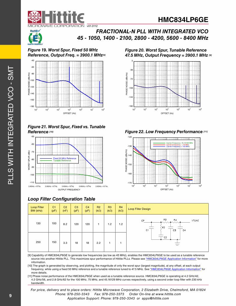
Figure 19. worst Spur, Fixed 50 Mhz reference, output Freq. = 3900.1 Mhz[9]
-180
-160
-140
-120
-100
-80
-60
-40
102
103
104
105
106
107
108
PH
AS
E N
OIS
E (
dB
c/H
z)
OFFSET (Hz)
Figure 20. worst Spur, tunable reference 47.5 Mhz, output Frequency = 3900.1 Mhz [9]
-180
-144
-108
-72
-36
0
102 103 104 105 106 107 108
PH
AS
E N
OIS
E (
dBc/
Hz)
OFFSET (Hz)
Figure 21. worst Spur, Fixed vs. tunable reference [10]
-110
-100
-90
-80
-70
-60
-50
3.9GHz +103Hz 3.9GHz +10
4Hz 3.9GHz +10
5Hz 3.9GHz +10
6Hz 3.9GHz +10
7Hz
Fixed 50 MHz ReferenceTunable Reference
WO
RS
T S
PU
R (
dB
c)
OUTPUT FREQUENCY
[9] Capability of hMC834LP6ge to generate low frequencies (as low as 45 Mhz), enables the hMC834LP6ge to be used as a tunable reference source into another hittite PLL. this maximizes spur performance of hittite PLLs. Please see “hMC834LP6ge application information” for more information.
[10] the graph is generated by observing, and plotting, the magnitude of only the worst spur (largest magnitude), at any offset, at each output frequency, while using a fixed 50 Mhz reference and a tunable reference tuned to 47.5 Mhz. see “hMC834LP6ge application information” for more details.
[11] Phase noise performance of the hMC834LP6ge when used as a tunable reference source. hMC834LP6ge is operating at 4.2 ghz/42, 4.2 ghz/56, and 2.8 ghz/62 for the 100 Mhz, 75 Mhz, and 45.16129 Mhz curves respectively, using a second order loop filter with 230 khz bandwidth.
Figure 22. low Frequency Performance [11]
-170
-160
-150
-140
-130
-120
102
103
104
105
106
107
108
Carrier Frequency 45.16129 MHzCarrier Frequency = 75 MHzCarrier Frequency = 100 MHz
PH
AS
E N
OIS
E (
dB
c/H
z)
OFFSET (Hz)
For price, delivery and to place orders: Hittite Microwave Corporation, 2 Elizabeth Drive, Chelmsford, MA 01824Phone: 978-250-3343 Fax: 978-250-3373 Order On-line at www.hittite.com
Application Support: Phone: 978-250-3343 or [email protected]
PLL
s w
ith
int
eg
rat
ed
VC
O -
sM
t
10
HMC834LP6GEv01.0112
Fractional-n Pll with integrated Vco45 - 1050, 1400 - 2100, 2800 - 4200, 5600 - 8400 Mhz
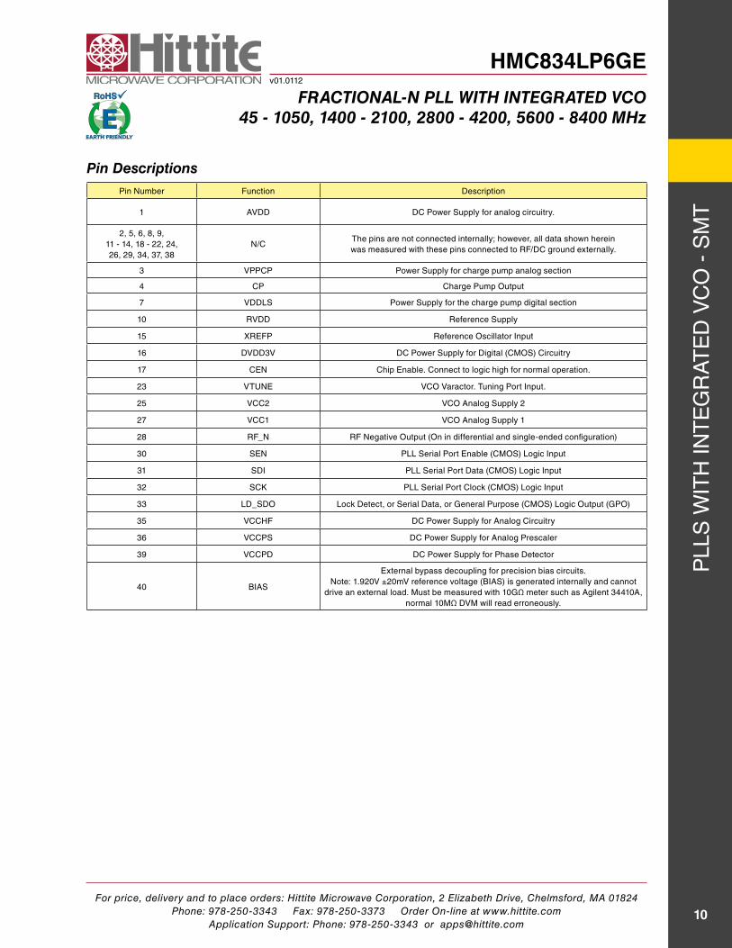
Pin descriptionsPin number Function description
1 aVdd dC Power supply for analog circuitry.
2, 5, 6, 8, 9, 11 - 14, 18 - 22, 24, 26, 29, 34, 37, 38
n/Cthe pins are not connected internally; however, all data shown herein was measured with these pins connected to rF/dC ground externally.
3 VPPCP Power supply for charge pump analog section
4 CP Charge Pump Output
7 VddLs Power supply for the charge pump digital section
10 rVdd reference supply
15 XreFP reference Oscillator input
16 dVdd3V dC Power supply for digital (CMOs) Circuitry
17 Cen Chip enable. Connect to logic high for normal operation.
23 VtUne VCO Varactor. tuning Port input.
25 VCC2 VCO analog supply 2
27 VCC1 VCO analog supply 1
28 rF_n rF negative Output (On in differential and single-ended configuration)
30 sen PLL serial Port enable (CMOs) Logic input
31 sdi PLL serial Port data (CMOs) Logic input
32 sCK PLL serial Port Clock (CMOs) Logic input
33 Ld_sdO Lock detect, or serial data, or general Purpose (CMOs) Logic Output (gPO)
35 VCChF dC Power supply for analog Circuitry
36 VCCPs dC Power supply for analog Prescaler
39 VCCPd dC Power supply for Phase detector
40 Bias
external bypass decoupling for precision bias circuits. note: 1.920V ±20mV reference voltage (Bias) is generated internally and cannot
drive an external load. Must be measured with 10gΩ meter such as agilent 34410a, normal 10MΩ dVM will read erroneously.
For price, delivery and to place orders: Hittite Microwave Corporation, 2 Elizabeth Drive, Chelmsford, MA 01824Phone: 978-250-3343 Fax: 978-250-3373 Order On-line at www.hittite.com
Application Support: Phone: 978-250-3343 or [email protected]
PLL
s w
ith
int
eg
rat
ed
VC
O -
sM
t
11
HMC834LP6GEv01.0112
Fractional-n Pll with integrated Vco45 - 1050, 1400 - 2100, 2800 - 4200, 5600 - 8400 Mhz
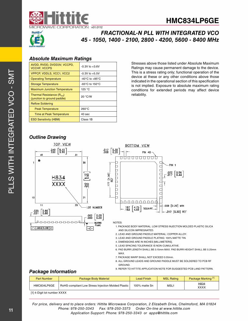
outline drawing
Part number Package Body Material Lead Finish MsL rating Package Marking [1]
hMC834LP6ge rohs-compliant Low stress injection Molded Plastic 100% matte sn MsL1h834XXXX
[1] 4-digit lot number XXXX
Package information
nOtes:
1. PaCKage BOdY MateriaL: LOw stress inJeCtiOn MOLded PLastiC siLiCa
and siLiCOn iMPregnated.
2. Lead and grOUnd PaddLe MateriaL: COPPer aLLOY.
3. Lead and grOUnd PaddLe PLating: 100% Matte tin.
4. diMensiOns are in inChes [MiLLiMeters].
5. Lead sPaCing tOLeranCe is nOn-CUMULatiVe.
6. Pad BUrr Length shaLL Be 0.15mm MaX. Pad BUrr height shaLL Be 0.25mm
MaX.
7. PaCKage warP shaLL nOt eXCeed 0.05mm.
8. aLL grOUnd Leads and grOUnd PaddLe MUst Be sOLdered tO PCB rF
grOUnd.
9. reFer tO hittite aPPLiCatiOn nOte FOr sUggested PCB Land Pattern.
absolute Maximum ratingsaVdd, rVdd, dVdd3V, VCCPd, VCChF, VCCPs
-0.3V to +3.6V
VPPCP, VddLs, VCC1, VCC2 -0.3V to +5.5V
Operating temperature -40°C to +85°C
storage temperature -65°C to 150°C
Maximum Junction temperature 125 °C
thermal resistance (rth) (junction to ground paddle)
20 °C/w
reflow soldering
Peak temperature 260°C
time at Peak temperature 40 sec
esd sensitivity (hBM) Class 1B
stresses above those listed under absolute Maximum ratings may cause permanent damage to the device. this is a stress rating only; functional operation of the device at these or any other conditions above those indicated in the operational section of this specification is not implied. exposure to absolute maximum rating conditions for extended periods may affect device reliability.
For price, delivery and to place orders: Hittite Microwave Corporation, 2 Elizabeth Drive, Chelmsford, MA 01824Phone: 978-250-3343 Fax: 978-250-3373 Order On-line at www.hittite.com
Application Support: Phone: 978-250-3343 or [email protected]
PLL
s w
ith
int
eg
rat
ed
VC
O -
sM
t
12
HMC834LP6GEv01.0112
Fractional-n Pll with integrated Vco45 - 1050, 1400 - 2100, 2800 - 4200, 5600 - 8400 Mhz
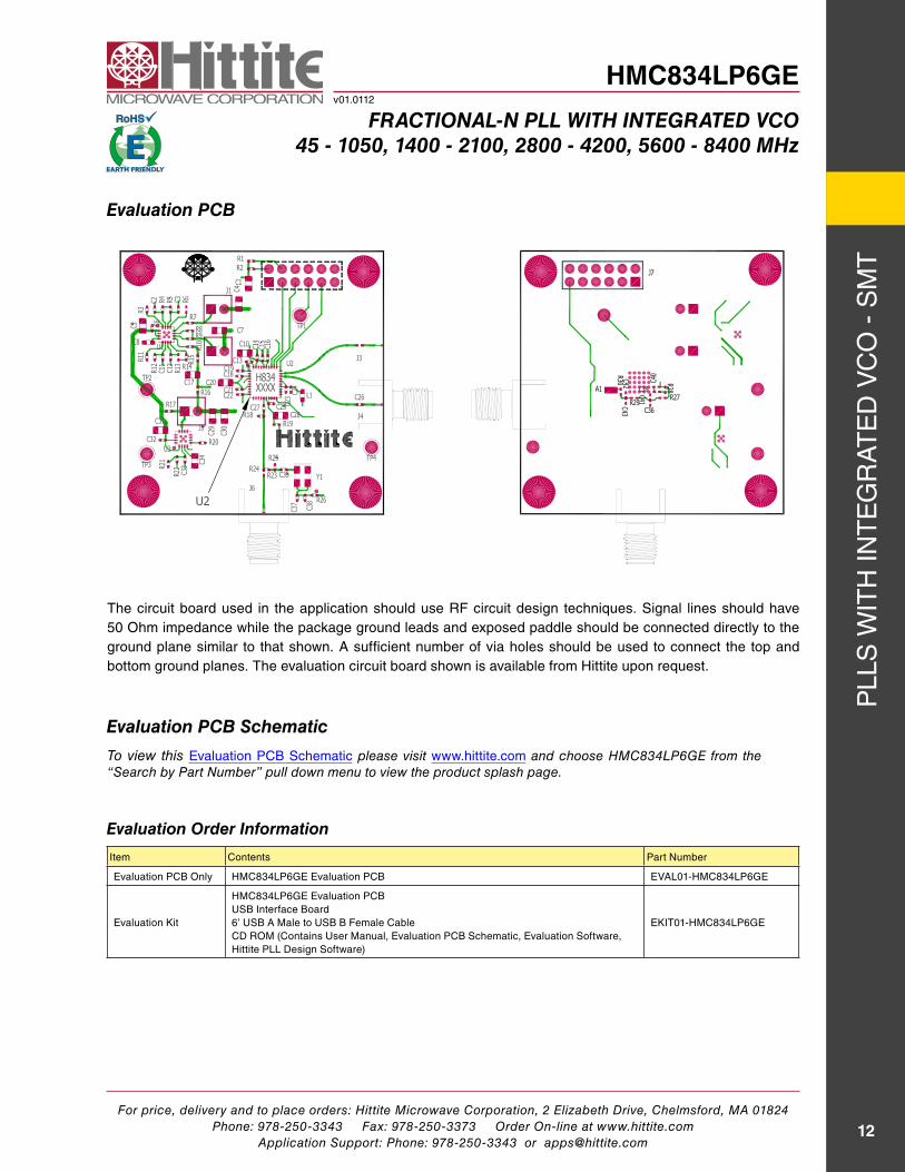
evaluation PcB Schematic
the circuit board used in the application should use rF circuit design techniques. signal lines should have 50 Ohm impedance while the package ground leads and exposed paddle should be connected directly to the ground plane similar to that shown. a sufficient number of via holes should be used to connect the top and bottom ground planes. the evaluation circuit board shown is available from hittite upon request.
To view this evaluation PCB schematic please visit www.hittite.com and choose HMC834LP6GE from the “Search by Part Number” pull down menu to view the product splash page.
evaluation PcB
item Contents Part number
evaluation PCB Only hMC834LP6ge evaluation PCB eVaL01-hMC834LP6ge
evaluation Kit
hMC834LP6ge evaluation PCBUsB interface Board6’ UsB a Male to UsB B Female CableCd rOM (Contains User Manual, evaluation PCB schematic, evaluation software, hittite PLL design software)
eKit01-hMC834LP6ge
evaluation order information
For price, delivery and to place orders: Hittite Microwave Corporation, 2 Elizabeth Drive, Chelmsford, MA 01824Phone: 978-250-3343 Fax: 978-250-3373 Order On-line at www.hittite.com
Application Support: Phone: 978-250-3343 or [email protected]
PLL
s w
ith
int
eg
rat
ed
VC
O -
sM
t
13
HMC834LP6GEv01.0112
Fractional-n Pll with integrated Vco45 - 1050, 1400 - 2100, 2800 - 4200, 5600 - 8400 Mhz
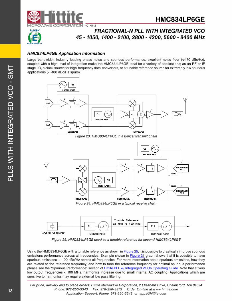
hMc834lP6ge application informationLarge bandwidth, industry leading phase noise and spurious performance, excellent noise floor (<-170 dBc/hz), coupled with a high level of integration make the hMC834LP6ge ideal for a variety of applications; as an rF or iF stage LO, a clock source for high-frequency data-converters, or a tunable reference source for extremely low spurious applications (~ -100 dBc/hz spurs).
Figure 23. HMC834LP6GE in a typical transmit chain
Figure 24. HMC834LP6GE in a typical receive chain
Figure 25. HMC834LP6GE used as a tunable reference for second HMC834LP6GE
Using the hMC834LP6ge with a tunable reference as shown in Figure 25, it is possible to drastically improve spurious emissions performance across all frequencies. example shown in Figure 21 graph shows that it is possible to have spurious emissions ~ -100 dBc/hz across all frequencies. For more information about spurious emissions, how they are related to the reference frequency, and how to tune the reference frequency for optimal spurious performance please see the “spurious Performance” section of hittite PLL w/ integraged VCOs Operating guide. note that at very low output frequencies < 100 Mhz, harmonics increase due to small internal aC coupling. applications which are sensitive to harmonics may require external low pass filtering.
For price, delivery and to place orders: Hittite Microwave Corporation, 2 Elizabeth Drive, Chelmsford, MA 01824Phone: 978-250-3343 Fax: 978-250-3373 Order On-line at www.hittite.com
Application Support: Phone: 978-250-3343 or [email protected]
PLL
s w
ith
int
eg
rat
ed
VC
O -
sM
t
14
HMC834LP6GEv01.0112
Fractional-n Pll with integrated Vco45 - 1050, 1400 - 2100, 2800 - 4200, 5600 - 8400 Mhz
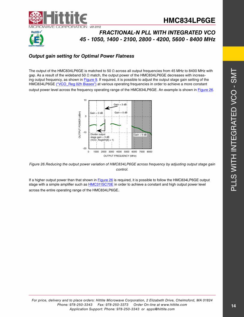
the output of the hMC834LP6ge is matched to 50 Ω across all output frequencies from 45 Mhz to 8400 Mhz with gap. as a result of the wideband 50 Ω match, the output power of the hMC834LP6ge decreases with increas-ing output frequency, as shown in Figure 9. if required, it is possible to adjust the output stage gain setting of the hMC834LP6ge (“VCO_reg 02h Biases”) at various operating frequencies in order to achieve a more constant
output power level across the frequency operating range of the hMC834LP6ge. an example is shown in Figure 26.
Figure 26.Reducing the output power variation of HMC834LP6GE across frequency by adjusting output stage gain control.
if a higher output power than that shown in Figure 26 is required, it is possible to follow the hMC834LP6ge output stage with a simple amplifier such as hMC311sC70e in order to achieve a constant and high output power level
across the entire operating range of the hMC834LP6ge.
output gain setting for optimal Power Flatness
-20
-10
0
10
0 1000 2000 3000 4000 5000 6000 7000 8000
OU
TP
UT
PO
WE
R (
dB
m)
OUTPUT FREQUENCY (MHz)
Gain = 0 dB
Gain = 9 dB
Gain = 3 dB
Divider outputstage gain = 3 dB(VCO_Reg02h[8] = 1)
Gain = 0 dB
For price, delivery and to place orders: Hittite Microwave Corporation, 2 Elizabeth Drive, Chelmsford, MA 01824Phone: 978-250-3343 Fax: 978-250-3373 Order On-line at www.hittite.com
Application Support: Phone: 978-250-3343 or [email protected]
PLL
s w
ith
int
eg
rat
ed
VC
O -
sM
t
15
HMC834LP6GEv01.0112
Fractional-n Pll with integrated Vco45 - 1050, 1400 - 2100, 2800 - 4200, 5600 - 8400 Mhz
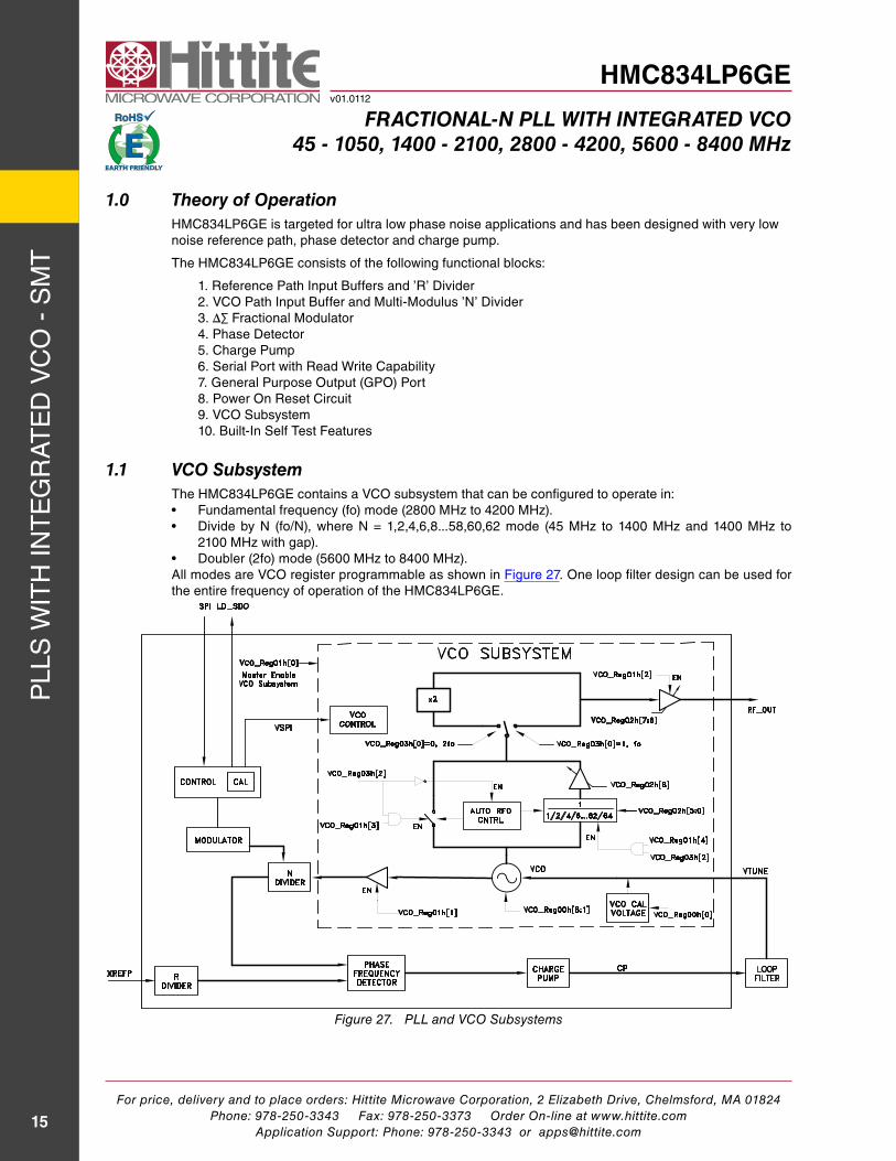
1.0 theory of operationhMC834LP6ge is targeted for ultra low phase noise applications and has been designed with very low noise reference path, phase detector and charge pump.
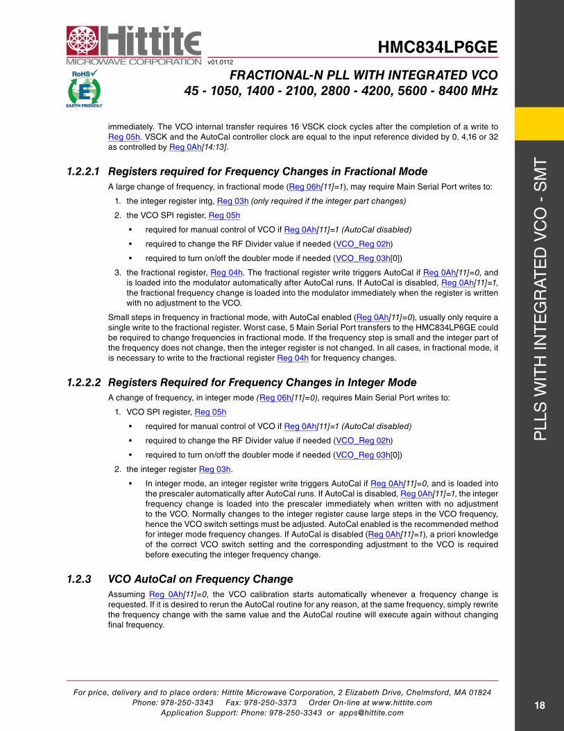
the hMC834LP6ge consists of the following functional blocks:
1. reference Path input Buffers and ’r’ divider2. VCO Path input Buffer and Multi-Modulus ’n’ divider3. Δ∑ Fractional Modulator4. Phase detector5. Charge Pump6. serial Port with read write Capability7. general Purpose Output (gPO) Port8. Power On reset Circuit9. VCO subsystem 10. Built-in self test Features
1.1 Vco Subsystemthe hMC834LP6ge contains a VCO subsystem that can be configured to operate in:• Fundamental frequency (fo) mode (2800 Mhz to 4200 Mhz).• divide by n (fo/n), where n = 1,2,4,6,8...58,60,62 mode (45 Mhz to 1400 Mhz and 1400 Mhz to
2100 Mhz with gap).• doubler (2fo) mode (5600 Mhz to 8400 Mhz).all modes are VCO register programmable as shown in Figure 27. One loop filter design can be used for the entire frequency of operation of the hMC834LP6ge.
Figure 27. PLL and VCO Subsystems
For price, delivery and to place orders: Hittite Microwave Corporation, 2 Elizabeth Drive, Chelmsford, MA 01824Phone: 978-250-3343 Fax: 978-250-3373 Order On-line at www.hittite.com
Application Support: Phone: 978-250-3343 or [email protected]
PLL
s w
ith
int
eg
rat
ed
VC
O -
sM
t
16
HMC834LP6GEv01.0112
Fractional-n Pll with integrated Vco45 - 1050, 1400 - 2100, 2800 - 4200, 5600 - 8400 Mhz
1.2 Vco calibration
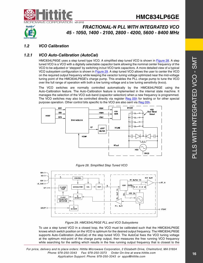
1.2.1 Vco auto-calibration (autocal)hMC834LP6ge uses a step tuned type VCO. a simplified step tuned VCO is shown in Figure 28. a step tuned VCO is a VCO with a digitally selectable capacitor bank allowing the nominal center frequency of the VCO to be adjusted or ‘stepped’ by switching in/out VCO tank capacitors. a more detailed view of a typical VCO subsystem configuration is shown in Figure 29. a step tuned VCO allows the user to center the VCO on the required output frequency while keeping the varactor tuning voltage optimized near the mid-voltage tuning point of the hMC834LP6ge’s charge pump. this enables the PLL charge pump to tune the VCO over the full range of operation with both a low tuning voltage and a low tuning sensitivity (kvco).
the VCO switches are normally controlled automatically by the hMC834LP6ge using the auto-Calibration feature. the auto-Calibration feature is implemented in the internal state machine. it manages the selection of the VCO sub-band (capacitor selection) when a new frequency is programmed. the VCO switches may also be controlled directly via register reg 05h for testing or for other special purpose operation. Other control bits specific to the VCO are also sent via reg 05h.
Figure 28. Simplified Step Tuned VCO
Figure 29. HMC834LP6GE PLL and VCO Subsystems
to use a step tuned VCO in a closed loop, the VCO must be calibrated such that the hMC834LP6ge knows which switch position on the VCO is optimum for the desired output frequency. the hMC834LP6ge supports auto-Calibration (autoCal) of the step tuned VCO. the autoCal fixes the VCO tuning voltage at the optimum mid-point of the charge pump output, then measures the free running VCO frequency while searching for the setting which results in the free running output frequency that is closest to the
For price, delivery and to place orders: Hittite Microwave Corporation, 2 Elizabeth Drive, Chelmsford, MA 01824Phone: 978-250-3343 Fax: 978-250-3373 Order On-line at www.hittite.com
Application Support: Phone: 978-250-3343 or [email protected]
PLL
s w
ith
int
eg
rat
ed
VC
O -
sM
t
17
HMC834LP6GEv01.0112
Fractional-n Pll with integrated Vco45 - 1050, 1400 - 2100, 2800 - 4200, 5600 - 8400 Mhz
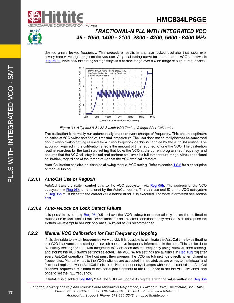
desired phase locked frequency. this procedure results in a phase locked oscillator that locks over a very narrow voltage range on the varactor. a typical tuning curve for a step tuned VCO is shown in Figure 30. note how the tuning voltage stays in a narrow range over a wide range of output frequencies.
0
1
2
3
4
5
920 960 1000 1040 1080 1120 1160
CALIBRATION FREQUENCY (MHz)
TU
NE
VO
LTA
GE
AF
TE
R C
ALI
BR
AT
ION
(V
)
50MHz PFD, 500kHz Tuning Steps, +25C256 Count Calibration ,195kHz Resolution31usec Total Cal Time
01531
Figure 30. A Typical 5-Bit 32 Switch VCO Tuning Voltage After Calibration
the calibration is normally run automatically once for every change of frequency. this ensures optimum selection of VCO switch settings vs. time and temperature. the user does not normally have to be concerned about which switch setting is used for a given frequency as this is handled by the autoCal routine. the accuracy required in the calibration affects the amount of time required to tune the VCO. the calibration routine searches for the best step setting that locks the VCO at the current programmed frequency, and ensures that the VCO will stay locked and perform well over it’s full temperature range without additional calibration, regardless of the temperature that the VCO was calibrated at.
auto-Calibration can also be disabled allowing manual VCO tuning. refer to section 1.2.2 for a description of manual tuning
1.2.1.1 autocal Use of reg05hautoCal transfers switch control data to the VCO subsystem via reg 05h. the address of the VCO subsystem in reg 05h is not altered by the autoCal routine. the address and id of the VCO subsystem in reg 05h must be set to the correct value before autoCal is executed. For more information see section 1.19.
1.2.1.2 auto-relock on lock detect Failureit is possible by setting reg 07h[13] to have the VCO subsystem automatically re-run the calibration routine and re-lock itself if Lock detect indicates an unlocked condition for any reason. with this option the system will attempt to re-Lock only once. auto-reLock is recommended.
1.2.2 Manual Vco calibration for Fast Frequency hoppingif it is desirable to switch frequencies very quickly it is possible to eliminate the autoCal time by calibrating the VCO in advance and storing the switch number vs frequency information in the host. this can be done by initially locking the PLL with integrated VCO on each desired frequency using autoCal, then reading, and storing the VCO switch settings selected. the VCO switch settings are available in reg 10h[7:0] after every autoCal operation. the host must then program the VCO switch settings directly when changing frequencies. Manual writes to the VCO switches are executed immediately as are writes to the integer and fractional registers when autoCal is disabled. hence frequency changes with manual control and autoCal disabled, requires a minimum of two serial port transfers to the PLL, once to set the VCO switches, and once to set the PLL frequency.
if autoCal is disabled reg 0ah[11]=1, the VCO will update its registers with the value written via reg 05h
For price, delivery and to place orders: Hittite Microwave Corporation, 2 Elizabeth Drive, Chelmsford, MA 01824Phone: 978-250-3343 Fax: 978-250-3373 Order On-line at www.hittite.com
Application Support: Phone: 978-250-3343 or [email protected]
PLL
s w
ith
int
eg
rat
ed
VC
O -
sM
t
18
HMC834LP6GEv01.0112
Fractional-n Pll with integrated Vco45 - 1050, 1400 - 2100, 2800 - 4200, 5600 - 8400 Mhz
immediately. the VCO internal transfer requires 16 VsCK clock cycles after the completion of a write to reg 05h. VsCK and the autoCal controller clock are equal to the input reference divided by 0, 4,16 or 32 as controlled by reg 0ah[14:13].
1.2.2.1 registers required for Frequency changes in Fractional Modea large change of frequency, in fractional mode (reg 06h[11]=1), may require Main serial Port writes to:
1. the integer register intg, reg 03h (only required if the integer part changes)
2. the VCO sPi register, reg 05h
• required for manual control of VCO if reg 0ah[11]=1 (AutoCal disabled)
• required to change the rF divider value if needed (VCO_reg 02h)
• required to turn on/off the doubler mode if needed (VCO_reg 03h[0])
3. the fractional register, reg 04h. the fractional register write triggers autoCal if reg 0ah[11]=0, and is loaded into the modulator automatically after autoCal runs. if autoCal is disabled, reg 0ah[11]=1, the fractional frequency change is loaded into the modulator immediately when the register is written with no adjustment to the VCO.
small steps in frequency in fractional mode, with autoCal enabled (reg 0ah[11]=0), usually only require a single write to the fractional register. worst case, 5 Main serial Port transfers to the hMC834LP6ge could be required to change frequencies in fractional mode. if the frequency step is small and the integer part of the frequency does not change, then the integer register is not changed. in all cases, in fractional mode, it is necessary to write to the fractional register reg 04h for frequency changes.
1.2.2.2 registers required for Frequency changes in integer Modea change of frequency, in integer mode (reg 06h[11]=0), requires Main serial Port writes to:
1. VCO sPi register, reg 05h
• required for manual control of VCO if reg 0ah[11]=1 (AutoCal disabled)
• required to change the rF divider value if needed (VCO_reg 02h)
• required to turn on/off the doubler mode if needed (VCO_reg 03h[0])
2. the integer register reg 03h.
• in integer mode, an integer register write triggers autoCal if reg 0ah[11]=0, and is loaded into the prescaler automatically after autoCal runs. if autoCal is disabled, reg 0ah[11]=1, the integer frequency change is loaded into the prescaler immediately when written with no adjustment to the VCO. normally changes to the integer register cause large steps in the VCO frequency, hence the VCO switch settings must be adjusted. autoCal enabled is the recommended method for integer mode frequency changes. if autoCal is disabled (reg 0ah[11]=1), a priori knowledge of the correct VCO switch setting and the corresponding adjustment to the VCO is required before executing the integer frequency change.
1.2.3 Vco autocal on Frequency changeassuming reg 0ah[11]=0, the VCO calibration starts automatically whenever a frequency change is requested. if it is desired to rerun the autoCal routine for any reason, at the same frequency, simply rewrite the frequency change with the same value and the autoCal routine will execute again without changing final frequency.
For price, delivery and to place orders: Hittite Microwave Corporation, 2 Elizabeth Drive, Chelmsford, MA 01824Phone: 978-250-3343 Fax: 978-250-3373 Order On-line at www.hittite.com
Application Support: Phone: 978-250-3343 or [email protected]
PLL
s w
ith
int
eg
rat
ed
VC
O -
sM
t
19
HMC834LP6GEv01.0112
Fractional-n Pll with integrated Vco45 - 1050, 1400 - 2100, 2800 - 4200, 5600 - 8400 Mhz
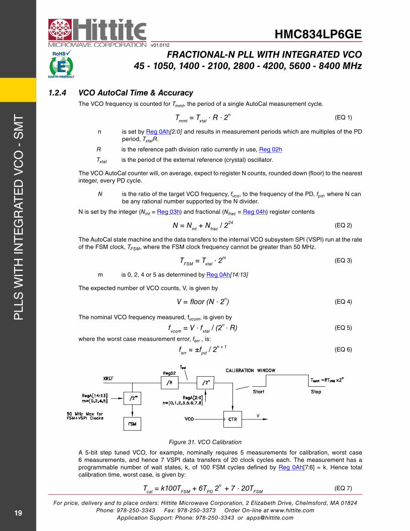
1.2.4 Vco autocal time & accuracythe VCO frequency is counted for Tmmt, the period of a single autoCal measurement cycle.
Tmmt = Txtal · R · 2n (eQ 1)
n is set by reg 0ah[2:0] and results in measurement periods which are multiples of the Pd period, TxtalR.
R is the reference path division ratio currently in use, reg 02h
Txtal is the period of the external reference (crystal) oscillator.
the VCO autoCal counter will, on average, expect to register n counts, rounded down (floor) to the nearest integer, every Pd cycle.
N is the ratio of the target VCO frequency, fvco, to the frequency of the Pd, fpd, where n can be any rational number supported by the n divider.
n is set by the integer (Nint = reg 03h) and fractional (Nfrac = reg 04h) register contents
N = Nint + Nfrac / 224 (eQ 2)
the autoCal state machine and the data transfers to the internal VCO subsystem sPi (VsPi) run at the rate of the FsM clock, TFSM, where the FsM clock frequency cannot be greater than 50 Mhz.
TFSM = Txtal · 2m (eQ 3)
m is 0, 2, 4 or 5 as determined by reg 0ah[14:13]
the expected number of VCO counts, V, is given by
V = floor (N · 2n) (eQ 4)
the nominal VCO frequency measured, fvcom, is given by
fvcom = V · fxtal / (2n · R) (eQ 5)
where the worst case measurement error, ferr , is:
ferr ≈ ±fpd / 2n + 1 (eQ 6)
Figure 31. VCO Calibration
a 5-bit step tuned VCO, for example, nominally requires 5 measurements for calibration, worst case 6 measurements, and hence 7 VsPi data transfers of 20 clock cycles each. the measurement has a programmable number of wait states, k, of 100 FsM cycles defined by reg 0ah[7:6] = k. hence total calibration time, worst case, is given by:
Tcal = k100TFSM + 6TPD 2n + 7 · 20TFSM(eQ 7)
For price, delivery and to place orders: Hittite Microwave Corporation, 2 Elizabeth Drive, Chelmsford, MA 01824Phone: 978-250-3343 Fax: 978-250-3373 Order On-line at www.hittite.com
Application Support: Phone: 978-250-3343 or [email protected]
PLL
s w
ith
int
eg
rat
ed
VC
O -
sM
t
20
HMC834LP6GEv01.0112
Fractional-n Pll with integrated Vco45 - 1050, 1400 - 2100, 2800 - 4200, 5600 - 8400 Mhz
or equivalently
Tcal = Txtal (6R · 2n + (140+100k) · 2m)where k = reg 0ah[7:6] decimal
(eQ 8)
For guaranteed hold of lock, across temperature extremes, the resolution should be better than 1/8th the frequency step caused by a VCO sub-band switch change. Better resolution settings will show no improvement.
1.2.4.1 Vco autocal examplethe VCO subsystem must satisfy the maximum fpd limited by the two following conditions:
a. n ≥ 16 (fint), n ≥ 20.0 (ffrac), where n = fVCO/ fpd
b. fpd ≤ 100 Mhz
suppose the VCO subsystem output frequency is to operate at 2.01 ghz. Our example crystal frequency is fxtal = 50 MHz, R=1, and m=0 (Figure 31), hence TFSM = 20 ns (50 Mhz). note, when using autoCal, the maximum autoCal Finite state Machine (FsM) clock cannot exceed 60 Mhz (see reg 0ah[14:13]). the FsM clock does not affect the accuracy of the measurement, it only affects the time to produce the result. this same clock is used to clock the 16 bit VCO serial port.
if time to change frequencies is not a concern, then one may set the calibration time for maximum accuracy, and therefore not be concerned with measurement resolution.
Using an input crystal of 50 Mhz (r=1 and fpd=50 Mhz) the times and accuracies for calibration using (eQ 6) and (eQ 8) are shown in table 1. where minimal tuning time is 1/8th of the VCO band spacing.
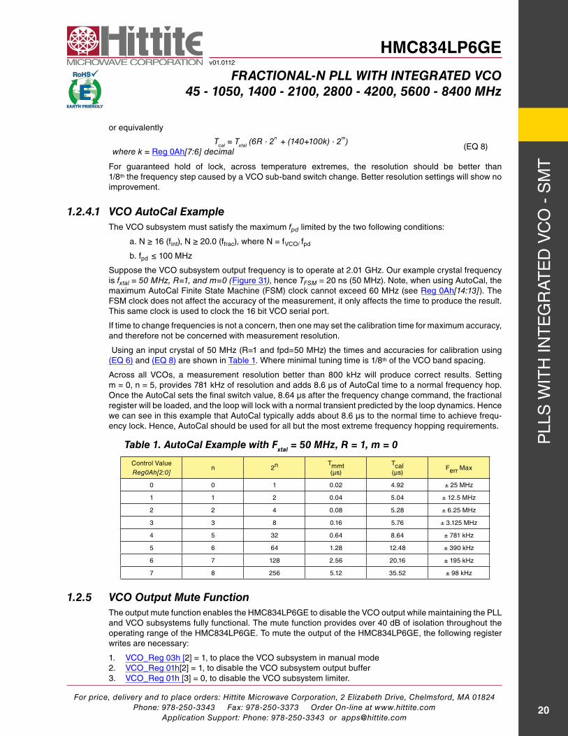
across all VCOs, a measurement resolution better than 800 khz will produce correct results. setting m = 0, n = 5, provides 781 khz of resolution and adds 8.6 µs of autoCal time to a normal frequency hop. Once the autoCal sets the final switch value, 8.64 µs after the frequency change command, the fractional register will be loaded, and the loop will lock with a normal transient predicted by the loop dynamics. hence we can see in this example that autoCal typically adds about 8.6 µs to the normal time to achieve frequ-ency lock. hence, autoCal should be used for all but the most extreme frequency hopping requirements.
table 1. autocal example with Fxtal = 50 Mhz, r = 1, m = 0
Control ValueReg0Ah[2:0]
n 2n tmmt(µs)
tcal(µs)
Ferr Max
0 0 1 0.02 4.92 ± 25 Mhz
1 1 2 0.04 5.04 ± 12.5 Mhz
2 2 4 0.08 5.28 ± 6.25 Mhz
3 3 8 0.16 5.76 ± 3.125 Mhz
4 5 32 0.64 8.64 ± 781 khz
5 6 64 1.28 12.48 ± 390 khz
6 7 128 2.56 20.16 ± 195 khz
7 8 256 5.12 35.52 ± 98 khz
1.2.5 Vco output Mute Functionthe output mute function enables the hMC834LP6ge to disable the VCO output while maintaining the PLL and VCO subsystems fully functional. the mute function provides over 40 dB of isolation throughout the operating range of the hMC834LP6ge. to mute the output of the hMC834LP6ge, the following register writes are necessary:
1. VCO_reg 03h [2] = 1, to place the VCO subsystem in manual mode2. VCO_reg 01h[2] = 1, to disable the VCO subsystem output buffer3. VCO_reg 01h [3] = 0, to disable the VCO subsystem limiter.
For price, delivery and to place orders: Hittite Microwave Corporation, 2 Elizabeth Drive, Chelmsford, MA 01824Phone: 978-250-3343 Fax: 978-250-3373 Order On-line at www.hittite.com
Application Support: Phone: 978-250-3343 or [email protected]
PLL
s w
ith
int
eg
rat
ed
VC
O -
sM
t
21
HMC834LP6GEv01.0112
Fractional-n Pll with integrated Vco45 - 1050, 1400 - 2100, 2800 - 4200, 5600 - 8400 Mhz
Please note that the VCO subsystem registers are not directly accessible. they are written to via PLL reg 05h. More information about VCO subsystem sPi in section 1.19.
1.3 Vco Built in test with autocalthe frequency limits of the VCO can be measured using the Bist features of the autoCal machine.
this is done by setting reg 0ah[10]=1 which freezes the VCO switches in one position. VCO switches may then be written manually, with the varactor biased at the nominal mid-rail voltage used for autoCal. For example to measure the VCO maximum frequency use switch 0, written to the VCO subsystem via reg 05h=[000000000 0000 VCOid]. where VCOid = ‘000’b.
if autoCal is enabled, (reg 0ah[11] = 0), and a new frequency is written, autoCal will run, but with switches frozen. the VCO frequency error relative to the command frequency will be measured and results written to reg 11h[19:0] where reg 11h[19] is the sign bit. the result will be written in terms of VCO count error (eQ 4). For example if the expected VCO is 2 ghz, reference is 50 Mhz, and n is 6, we expect to measure 2560 counts. if we measure a difference of -5 counts in reg 11h, then it means we actually measured 2555 counts. hence the actual frequency of the VCO is 5/2560 low, or 1.99609375 ghz, ±1 Count ~ ±781 khz.
1.4 Spurious Performance
1.4.1 integer operation and reference Spuriousthe VCO always operates at an integer multiple of the Pd frequency in an integer synthesizer. in general, spurious signals originating from an integer synthesizer can only occur at multiples of the Pd frequency. these unwanted outputs closest to the carrier are often simply referred to as reference sidebands. Unwanted reference harmonics can also exist far from the carrier due to circuit isolation.
spurs unrelated to the reference frequency must originate from outside sources. external spurious sources can modulate the VCO indirectly through power supplies, ground, or output ports, or bypass the loop filter due to poor isolation of the filter. it can also simply add to the output of the PLL.
reference spuri ous levels are typically below -100 dBc with a well designed board layout. a regulator with low noise and high power supply rejection, such as the hMC1060LP3e, is recommended to minimize external spurious sources.
reference spurious levels of below -100 dBc require superb board isolation of power supplies, isolation of the VCO from the digital switching of the synthesizer and isolation of the VCO load from the synthesizer. typical board layout, regulator design, eval boards and application information are available for very low spurious operation. Operation with lower levels of isolation in the application circuit board, from those rec-ommended by hittite, can result in higher spurious levels.
if the application environment contains other interfering frequencies unrelated to the Pd fre quency, and if the application isolation from the board layout and regulation are insufficient, the unwanted interfering frequencies will mix with the desired synthesizer output and cause additional spurious emissions. the level of these emissions is dependant upon isolation and supply regulation or rejection (Psrr).
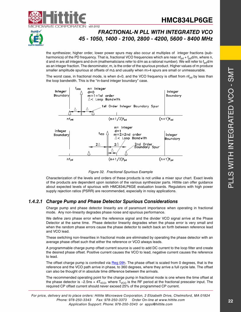
1.4.2 Fractional operation and SpuriousUnlike an integer PLL, spurious signals in a fractional PLL can occur due to the fact that the VCO operates at frequencies unrelated to the Pd frequency. hence intermodulation of the VCO and the Pd harmonics can cause spurious sidebands. spurious emissions are largest when the VCO operates very close to an integer multiple of the Pd. when the VCO operates exactly at a harmonic of the Pd then, no in-close mixing products are present.
as shown in Figure 32, interference is always present at multiples of the Pd frequency, fpd, and the VCO frequency, fvco. the difference, Δ, between the VCO frequency and the nearest har monic of the reference, will create what are referred to as integer boundary spurs. depending upon the mode of operation of
For price, delivery and to place orders: Hittite Microwave Corporation, 2 Elizabeth Drive, Chelmsford, MA 01824Phone: 978-250-3343 Fax: 978-250-3373 Order On-line at www.hittite.com
Application Support: Phone: 978-250-3343 or [email protected]
PLL
s w
ith
int
eg
rat
ed
VC
O -
sM
t
22
HMC834LP6GEv01.0112
Fractional-n Pll with integrated Vco45 - 1050, 1400 - 2100, 2800 - 4200, 5600 - 8400 Mhz
the synthesizer, higher order, lower power spurs may also occur at multiples of integer fractions (sub-harmonics) of the Pd frequency. that is, fractional VCO frequencies which are near nfpd + fpdd/m, where n, d and m are all integers and d<m (mathematicians refer to d/m as a rational num ber). we will refer to fpdd/m as an integer fraction. the denominator, m, is the order of the spurious product. higher values of m produce smaller amplitude spurious at offsets of mΔ and usually when m>4 spurs are small or unmeasurable.
the worst case, in fractional mode, is when d=0, and the VCO frequency is offset from nfpd by less than the loop bandwidth. this is the “in-band integer boundary” case.
Figure 32. Fractional Spurious Example
Characterization of the levels and orders of these products is not unlike a mixer spur chart. exact levels of the products are dependent upon isolation of the various synthesizer parts. hittite can offer guidance about expected levels of spurious with hMC834LP6ge evaluation boards. regulators with high power supply rejection ratios (Psrr) are recommended, especially in noisy applications.
1.4.2.1 charge Pump and Phase detector Spurious considerationsCharge pump and phase detector linearity are of paramount importance when operating in fractional mode. any non-linearity degrades phase noise and spurious performance.
we define zero phase error when the reference signal and the divider VCO signal arrive at the Phase detector at the same time. Phase detector linearity degrades when the phase error is very small and when the random phase errors cause the phase detector to switch back an forth between reference lead and VCO lead.
these switching non-linearities in fractional mode are eliminated by operating the phase detector with an average phase offset such that either the reference or VCO always leads.
a programmable charge pump offset current source is used to add dC current to the loop filter and create the desired phase offset. Positive current causes the VCO to lead, negative current causes the reference to lead.
the offset charge pump is controlled via reg 09h. the phase offset is scaled from 0 degrees, that is the reference and the VCO path arrive in phase, to 360 degrees, where they arrive a full cycle late. the offset can also be thought of in absolute time difference between the arrivals.
the recommended operating point for the charge pump in fractional mode is one where the time offset at the phase detector is ~2.5ns + 4tVCO, where tVCO is the rF period at the fractional prescaler input. the required CP offset current should never exceed 25% of the programmed CP current.
For price, delivery and to place orders: Hittite Microwave Corporation, 2 Elizabeth Drive, Chelmsford, MA 01824Phone: 978-250-3343 Fax: 978-250-3373 Order On-line at www.hittite.com
Application Support: Phone: 978-250-3343 or [email protected]
PLL
s w
ith
int
eg
rat
ed
VC
O -
sM
t
23
HMC834LP6GEv01.0112
Fractional-n Pll with integrated Vco45 - 1050, 1400 - 2100, 2800 - 4200, 5600 - 8400 Mhz
the specific level of charge pump offset current reg 09h[20:14] is determined by this time offset, the comparison frequency and the charge pump current:
( ) ( )( )92.5 10 4 sec ,0.25required CP Offset min VCO comparison CP CPT F I I− • + • • • • =
where:
TVCO: is the RF period at the fractional prescaler input
ICP: is the full scale current setting of the switching charge pump reg 09h[6:0] reg 09h[13:7]
(eQ 9)
Operation with charge pump offset influences the required configuration of the Lock detect function. refer to the description of Lock detect function in section 1.11. note that this calculation can be performed for the center frequency of the VCO, and does not need refinement for small differences < 25 % in center frequencies.
another factor in the spectral performance in Fractional Mode is the choice of the delta-sigma Modulator mode. Mode a can offer better in-band spectral performance (inside the loop bandwidth) while Mode B offers better out of band performance. see reg 06h[3:2] for dsM mode selection. Finally, all fractional synthesizers cre ate fractional spurs at some level. hittite offers the lowest level fractional spurious in the indus try in an integrated solution.
1.4.2.2 Spurious related to channel Step Size (channel Spurs)Many fractional PLLs also create spurious emissions at offsets which are multiples of the channel step size. we refer to these as Channel spurs. it is common in the industry to set the channel step size by use of the so-called modulus. For example, channel step size of 100 khz requires a small modulus related to the step size, and often results in 100 khz Channel spurs.
the hMC834LP6ge uses a large fixed modulus unrelated to the channel step size. as a result, the hMC834LP6ge has extremely low or unmeasurable Channel spurs. in addition exact Frequency Mode (1.12.2.2) allows exact channel step size with no Channel spurs.
the lack of Channel spurs means that the hMC834LP6ge has large regions of operation between integer Boundaries with little or no spurs of any kind. Large spurious free zones enable the hMC834LP6ge to be used with a tunable reference, to effectively move the spur free zones and hence achieve spur-free operation at all frequencies. the resulting PLL is virtually spur-free at all frequencies.
For more information see 1.4.2.3.
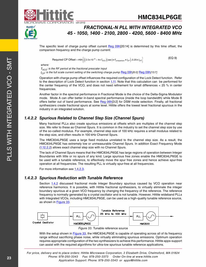
1.4.2.3 Spurious reduction with tunable referencesection 1.4.2 discussed fractional mode integer Boundary spurious caused by VCO operation near reference harmonics. it is possible, with hittite fractional synthesizers, to virtually eliminate the integer boundary spurious at a given VCO frequency by changing the frequency of the reference. the reference frequency is normally generated by a crystal oscillator and is not tunable. however, hittite wideband PLLs with integrated VCOs, including hMC834LP6ge, can be used as a high-quality tunable reference source, as shown in Figure 33.
Figure 33. tunable reference source
with the setup shown in Figure 33, the hMC834LP6ge is capable of operating across all of its frequency range without sacrificing phase noise, while virtually eliminating spurious emissions. Optimum operation requires appropriate configuration of the two synthesizers to achieve this performance. hittite apps-support can assist with the required algorithms for ultra-low spurious tunable reference applications.
For price, delivery and to place orders: Hittite Microwave Corporation, 2 Elizabeth Drive, Chelmsford, MA 01824Phone: 978-250-3343 Fax: 978-250-3373 Order On-line at www.hittite.com
Application Support: Phone: 978-250-3343 or [email protected]
PLL
s w
ith
int
eg
rat
ed
VC
O -
sM
t
24
HMC834LP6GEv01.0112
Fractional-n Pll with integrated Vco45 - 1050, 1400 - 2100, 2800 - 4200, 5600 - 8400 Mhz
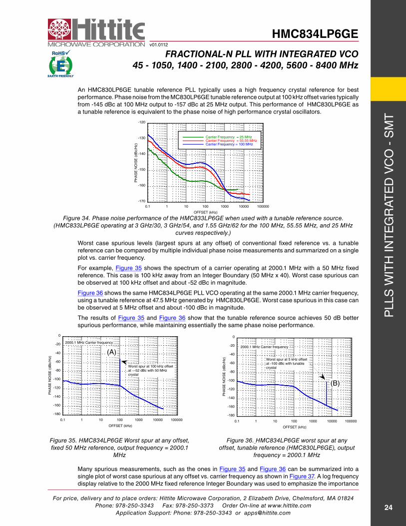
an hMC830LP6ge tunable reference PLL typically uses a high frequency crystal reference for best performance. Phase noise from the MC830LP6ge tunable reference output at 100 khz offset varies typically from -145 dBc at 100 Mhz output to -157 dBc at 25 Mhz output. this performance of hMC830LP6ge as a tunable reference is equivalent to the phase noise of high performance crystal oscillators.
Figure 34. Phase noise performance of the HMC833LP6GE
-170
-160
-150
-140
-130
-120
0.1 1 10 100 1000 10000 100000
Carrier Frequency = 25 MHzCarrier Frequency = 55.55 MHzCarrier Frequency = 100 MHz
PH
AS
E N
OIS
E (
dB
c/H
z)
OFFSET (kHz)
when used with a tunable reference source. (HMC833LP6GE operating at 3 GHz/30, 3 GHz/54, and 1.55 GHz/62 for the 100 MHz, 55.55 MHz, and 25 MHz
curves respectively.)
worst case spurious levels (largest spurs at any offset) of conventional fixed reference vs. a tunable reference can be compared by multiple individual phase noise measurements and summarized on a single plot vs. carrier frequency.
For example, Figure 35 shows the spectrum of a carrier operating at 2000.1 Mhz with a 50 Mhz fixed reference. this case is 100 khz away from an integer Boundary (50 Mhz x 40). worst case spurious can be observed at 100 khz offset and about -52 dBc in magnitude.
Figure 36 shows the same hMC834LP6ge PLL VCO operating at the same 2000.1 Mhz carrier frequency, using a tunable reference at 47.5 Mhz generated by hMC830LP6ge. worst case spurious in this case can be observed at 5 Mhz offset and about -100 dBc in magnitude.
the results of Figure 35 and Figure 36 show that the tunable reference source achieves 50 dB better spurious performance, while maintaining essentially the same phase noise performance.
-180
-160
-140
-120
-100
-80
-60
-40
-20
0
0.1 1 10 100 1000 10000 100000
PH
AS
E N
OIS
E (
dB
c/H
z)
OFFSET (kHz)
(A)
2000.1 MHz Carrier frequency
Worst spur at 100 kHz offset at ~-52 dBc with 50 MHz crystal
-180
-160
-140
-120
-100
-80
-60
-40
-20
0
0.1 1 10 100 1000 10000 100000
PH
AS
E N
OIS
E (
dB
c/H
z)
OFFSET (kHz)
(B)
2000.1 MHz Carrier frequency
Worst spur at 5 kHz offset at -100 dBc with tunable crystal
Figure 35. HMC834LP6GE Worst spur at any offset, fixed 50 MHz reference, output frequency = 2000.1
MHz
Figure 36. HMC834LP6GE worst spur at any offset, tunable reference (HMC830LP6GE), output
frequency = 2000.1 MHz
Many spurious measurements, such as the ones in Figure 35 and Figure 36 can be summarized into a single plot of worst case spurious at any offset vs. carrier frequency as shown in Figure 37. a log frequency display relative to the 2000 Mhz fixed reference integer Boundary was used to emphasize the importance
For price, delivery and to place orders: Hittite Microwave Corporation, 2 Elizabeth Drive, Chelmsford, MA 01824Phone: 978-250-3343 Fax: 978-250-3373 Order On-line at www.hittite.com
Application Support: Phone: 978-250-3343 or [email protected]
PLL
s w
ith
int
eg
rat
ed
VC
O -
sM
t
25
HMC834LP6GEv01.0112
Fractional-n Pll with integrated Vco45 - 1050, 1400 - 2100, 2800 - 4200, 5600 - 8400 Mhz
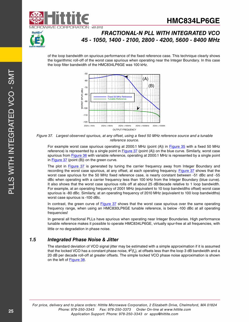
of the loop bandwidth on spurious performance of the fixed reference case. this technique clearly shows the logarithmic roll-off of the worst case spurious when operating near the integer Boundary. in this case the loop filter bandwidth of the hMC834LP6ge was 100 khz.
Figure 37.
-120
-110
-100
-90
-80
-70
-60
-50
2GHz +1kHz 2GHz +10kHz 2GHz +100kHz 2GHz +1000kHz 2GHz +10000kHz
Fixed 50 MHz ReferenceTunable Reference
WO
RS
T S
PU
R (
dB
c)
OUTPUT FREQUENCY
(A)
(B)
Largest observed spurious, at any offset, using a fixed 50 MHz reference source and a tunable reference source.
For example worst case spurious operating at 2000.1 Mhz (point (a)) in Figure 35 with a fixed 50 Mhz reference) is represented by a single point in Figure 37 (point (a)) on the blue curve. similarly, worst case spurious from Figure 36 with variable reference, operating at 2000.1 Mhz is represented by a single point in Figure 37 (point (B)) on the green curve.
the plot in Figure 37 is generated by tuning the carrier frequency away from integer Boundary and recording the worst case spurious, at any offset, at each operating frequency. Figure 37 shows that the worst case spurious for the 50 Mhz fixed reference case, is nearly constant between -51 dBc and -55 dBc when operating with a carrier frequency less than 100 khz from the integer Boundary (blue curve). it also shows that the worst case spurious rolls off at about 25 dB/decade relative to 1 loop bandwidth. For example, at an operating frequency of 2001 Mhz (equivalent to 10 loop bandwidths offset) worst case spurious is -80 dBc. similarly, at an operating frequency of 2010 Mhz (equivalent to 100 loop bandwidths) worst case spurious is -100 dBc.
in contrast, the green curve of Figure 37 shows that the worst case spurious over the same operating frequency range, when using an hMC830LP6ge tunable reference, is below -100 dBc at all operating frequencies!
in general all fractional PLLs have spurious when operating near integer Boundaries. high performance tunable reference makes it possible to operate hMC834LP6ge, virtually spur-free at all frequencies, with little or no degradation in phase noise.
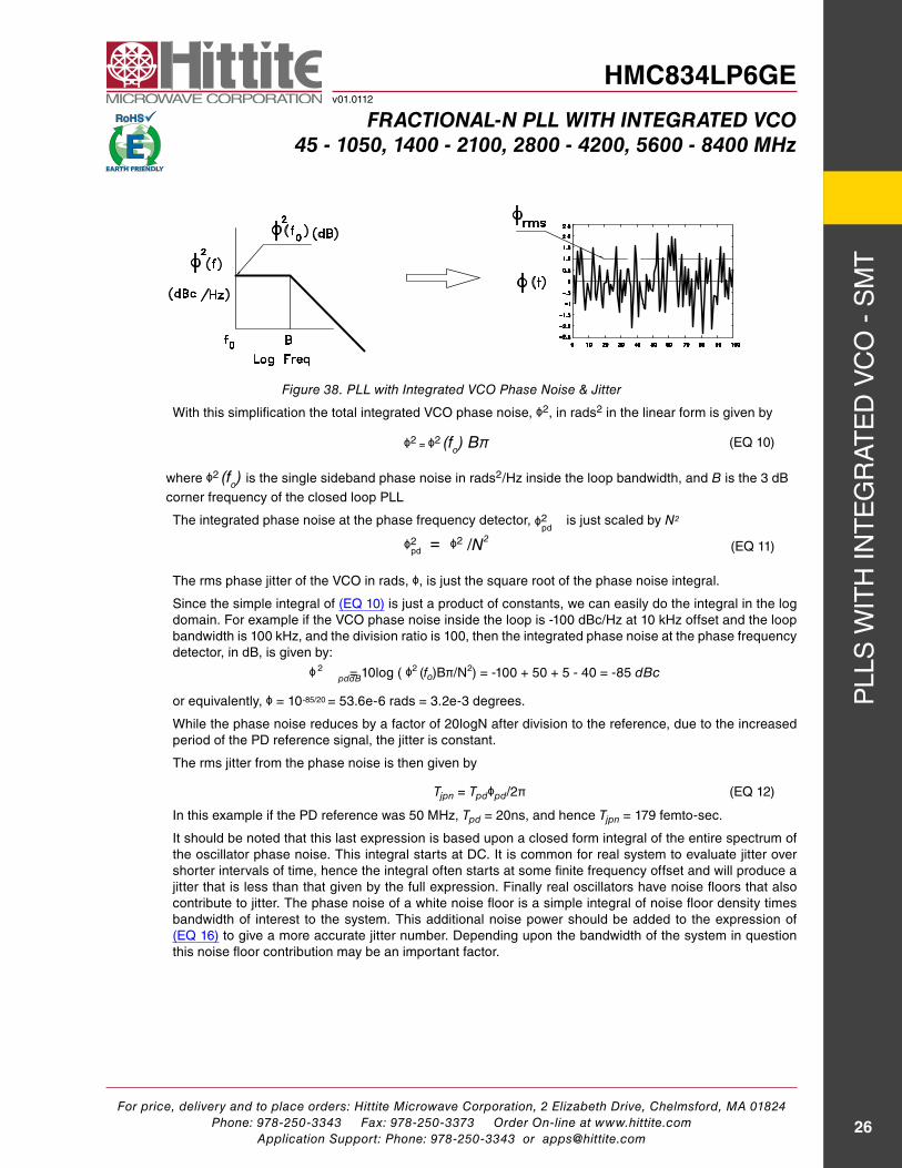
1.5 integrated Phase noise & Jitterthe standard deviation of VCO signal jitter may be estimated with a simple approximation if it is assumed that the locked VCO has a constant phase noise, o | 2(fo), at offsets less than the loop 3 dB bandwidth and a 20 dB per decade roll-off at greater offsets. the simple locked VCO phase noise approximation is shown on the left of Figure 38.
For price, delivery and to place orders: Hittite Microwave Corporation, 2 Elizabeth Drive, Chelmsford, MA 01824Phone: 978-250-3343 Fax: 978-250-3373 Order On-line at www.hittite.com
Application Support: Phone: 978-250-3343 or [email protected]
PLL
s w
ith
int
eg
rat
ed
VC
O -
sM
t
26
HMC834LP6GEv01.0112
Fractional-n Pll with integrated Vco45 - 1050, 1400 - 2100, 2800 - 4200, 5600 - 8400 Mhz
Figure 38. PLL with Integrated VCO Phase Noise & Jitter
with this simplification the total integrated VCO phase noise, o | 2, in rads2 in the linear form is given by
o | 2 = o | 2 (fo) Bπ (eQ 10)
where o | 2 (fo) is the single sideband phase noise in rads2/hz inside the loop bandwidth, and B is the 3 dB corner frequency of the closed loop PLL
the integrated phase noise at the phase frequency detector, o | 2 pd
is just scaled by N2
/N2=o | 2 pd
o | 2 (eQ 11)
the rms phase jitter of the VCO in rads, o | , is just the square root of the phase noise integral.
since the simple integral of (eQ 10) is just a product of constants, we can easily do the integral in the log domain. For example if the VCO phase noise inside the loop is -100 dBc/hz at 10 khz offset and the loop bandwidth is 100 khz, and the division ratio is 100, then the integrated phase noise at the phase frequency detector, in dB, is given by:
o | 2 = 10log ( o | 2 (fo)Bπ/n2) = -100 + 50 + 5 - 40 = -85 dBcpddB
or equivalently, o | = 10-85/20 = 53.6e-6 rads = 3.2e-3 degrees.
while the phase noise reduces by a factor of 20logn after division to the reference, due to the increased period of the Pd reference signal, the jitter is constant.
the rms jitter from the phase noise is then given by
Tjpn = Tpdo | pd/2π (eQ 12)
in this example if the Pd reference was 50 Mhz, Tpd = 20ns, and hence Tjpn = 179 femto-sec.
it should be noted that this last expression is based upon a closed form integral of the entire spectrum of the oscillator phase noise. this integral starts at dC. it is common for real system to evaluate jitter over shorter intervals of time, hence the integral often starts at some finite frequency offset and will produce a jitter that is less than that given by the full expression. Finally real oscillators have noise floors that also contribute to jitter. the phase noise of a white noise floor is a simple integral of noise floor density times bandwidth of interest to the system. this additional noise power should be added to the expression of (eQ 16) to give a more accurate jitter number. depending upon the bandwidth of the system in question this noise floor contribution may be an important factor.
For price, delivery and to place orders: Hittite Microwave Corporation, 2 Elizabeth Drive, Chelmsford, MA 01824Phone: 978-250-3343 Fax: 978-250-3373 Order On-line at www.hittite.com
Application Support: Phone: 978-250-3343 or [email protected]
PLL
s w
ith
int
eg
rat
ed
VC
O -
sM
t
27
HMC834LP6GEv01.0112
Fractional-n Pll with integrated Vco45 - 1050, 1400 - 2100, 2800 - 4200, 5600 - 8400 Mhz
1.6 reference input Stage
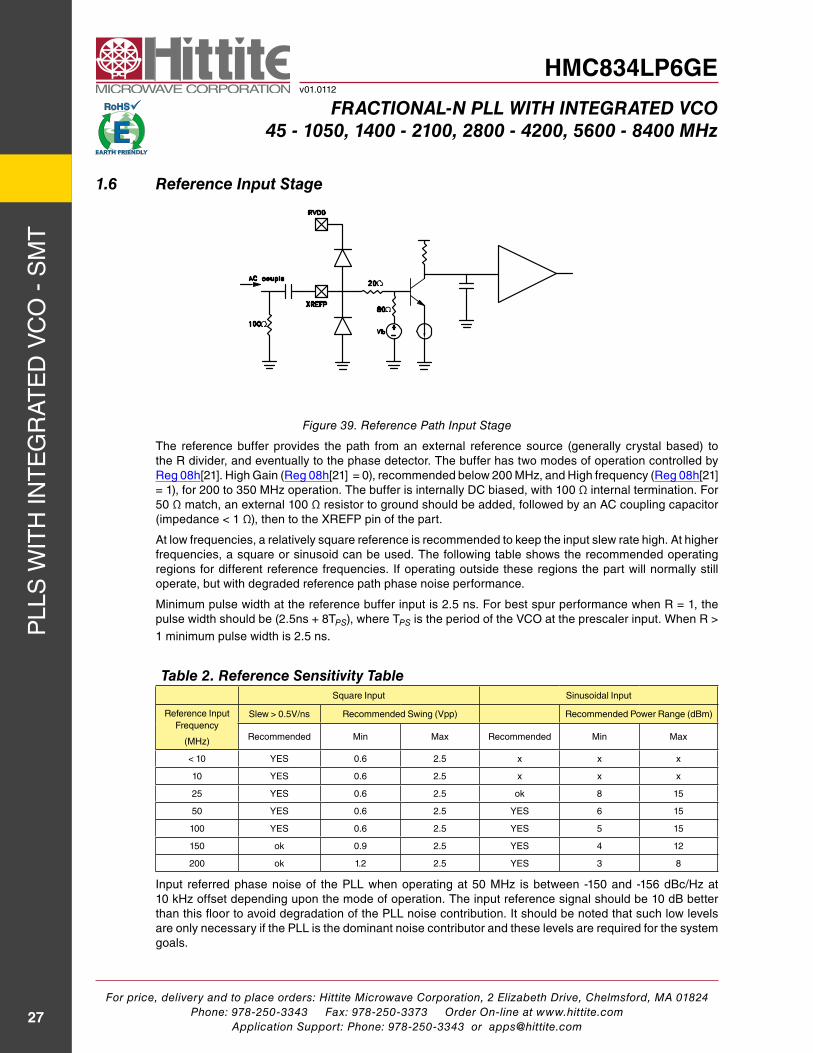
Figure 39. Reference Path Input Stage
the reference buffer provides the path from an external reference source (generally crystal based) to the r divider, and eventually to the phase detector. the buffer has two modes of operation controlled by reg 08h[21]. high gain (reg 08h[21] = 0), recommended below 200 Mhz, and high frequency (reg 08h[21] = 1), for 200 to 350 Mhz operation. the buffer is internally dC biased, with 100 Ω internal termination. For 50 Ω match, an external 100 Ω resistor to ground should be added, followed by an aC coupling capacitor (impedance < 1 Ω), then to the XreFP pin of the part.
at low frequencies, a relatively square reference is recommended to keep the input slew rate high. at higher frequencies, a square or sinusoid can be used. the following table shows the recommended operating regions for different reference frequencies. if operating outside these regions the part will normally still operate, but with degraded reference path phase noise performance.
Minimum pulse width at the reference buffer input is 2.5 ns. For best spur performance when r = 1, the pulse width should be (2.5ns + 8tPS), where tPS is the period of the VCO at the prescaler input. when r > 1 minimum pulse width is 2.5 ns.
table 2. reference Sensitivity tablesquare input sinusoidal input
reference input Frequency
(Mhz)
slew > 0.5V/ns recommended swing (Vpp) recommended Power range (dBm)
recommended Min Max recommended Min Max
< 10 Yes 0.6 2.5 x x x
10 Yes 0.6 2.5 x x x
25 Yes 0.6 2.5 ok 8 15
50 Yes 0.6 2.5 Yes 6 15
100 Yes 0.6 2.5 Yes 5 15
150 ok 0.9 2.5 Yes 4 12
200 ok 1.2 2.5 Yes 3 8
input referred phase noise of the PLL when operating at 50 Mhz is between -150 and -156 dBc/hz at 10 khz offset depending upon the mode of operation. the input reference signal should be 10 dB better than this floor to avoid deg radation of the PLL noise contribution. it should be noted that such low levels are only necessary if the PLL is the dominant noise contributor and these levels are required for the system goals.
For price, delivery and to place orders: Hittite Microwave Corporation, 2 Elizabeth Drive, Chelmsford, MA 01824Phone: 978-250-3343 Fax: 978-250-3373 Order On-line at www.hittite.com
Application Support: Phone: 978-250-3343 or [email protected]
PLL
s w
ith
int
eg
rat
ed
VC
O -
sM
t
28
HMC834LP6GEv01.0112
Fractional-n Pll with integrated Vco45 - 1050, 1400 - 2100, 2800 - 4200, 5600 - 8400 Mhz
1.7 reference Path ’r’ dividerthe reference path “r” divider is based on a 14-bit counter and can divide input signals by values from 1 to 16,383 and is controlled by rdiv (reg 02h).
Minimum pulse width at the reference buffer input is 2.5 ns. For best spur performance when r = 1, the pulse width should be (2.5 ns + 8tps), where tps is the period of the VCO at the prescaler input. when r > 1 minimum pulse width is 2.5 ns.
1.8 rF Path ’n’ dividerthe main rF path divider is capable of average divide ratios between 219-5 (524,283) and 20 in fractional mode, and 219-1 (524,287) to 16 in integer mode. the VCO frequency range divided by the minimum n divider value will place practical restrictions on the maximum usable Pd frequency. For example a VCO operating at 1.5 ghz in fractional mode with a minimum n divider value of 20 will have a maximum Pd frequency of 75 Mhz.
1.9 charge Pump & Phase detectorthe Phase detector (Pd) has two inputs, one from the reference path divider and one from the rF path divider. when in lock these two inputs are at the same average frequency and are fixed at a constant average phase offset with respect to each other. we refer to the frequency of operation of the Pd as fpd. Most formulae related to step size, delta-sigma modulation, timers etc., are functions of the operating frequency of the Pd, fpd. fpd is also referred to as the comparison frequency of the Pd.
the Pd compares the phase of the rF path signal with that of the reference path signal and controls the charge pump output current as a linear function of the phase difference between the two signals. the output current varies linearly over a full ±2π radians (±360°) of input phase difference.
1.10 Phase detector FunctionsPhase detector register reg 0Bh allows manual access to control special phase detector features.
PD_up_en (reg 0Bh[5]), if 0, masks the Pd up output, which prevents the charge pump from pumping up.̀
PD_dn_en (reg 0Bh[6]), if 0, masks the Pd down output, which prevents the charge pump from pumping down.
Clearing both PD_up_en and PD_dn_en effectively tri-states the charge pump while leaving all other functions operating internally.
Pd Force UP reg 0Bh[9] = 1 and Pd Force dn reg 0Bh[10] = 1 allows the charge pump to be forced up or down respectively. this will force the VCO to the ends to the tuning range which can be useful in test of the VCO.
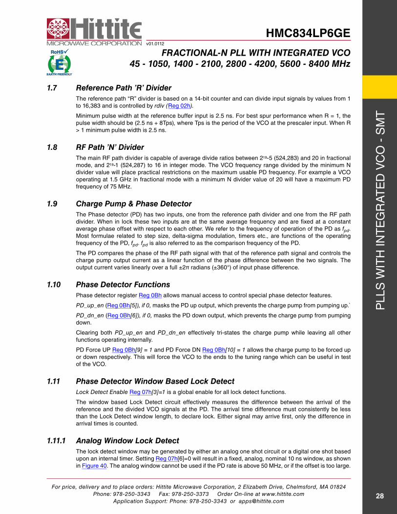
1.11 Phase detector window Based lock detectLock Detect Enable reg 07h[3]=1 is a global enable for all lock detect functions.
the window based Lock detect circuit effectively measures the difference between the arrival of the reference and the divided VCO signals at the Pd. the arrival time difference must consistently be less than the Lock detect window length, to declare lock. either signal may arrive first, only the difference in arrival times is counted.
1.11.1 analog window lock detectthe lock detect window may be generated by either an analog one shot circuit or a digital one shot based upon an internal timer. setting reg 07h[6]=0 will result in a fixed, analog, nominal 10 ns window, as shown in Figure 40. the analog window cannot be used if the Pd rate is above 50 Mhz, or if the offset is too large.
For price, delivery and to place orders: Hittite Microwave Corporation, 2 Elizabeth Drive, Chelmsford, MA 01824Phone: 978-250-3343 Fax: 978-250-3373 Order On-line at www.hittite.com
Application Support: Phone: 978-250-3343 or [email protected]
PLL
s w
ith
int
eg
rat
ed
VC
O -
sM
t
29
HMC834LP6GEv01.0112
Fractional-n Pll with integrated Vco45 - 1050, 1400 - 2100, 2800 - 4200, 5600 - 8400 Mhz
Figure 40. Normal Lock Detect Window - Integer Mode, Zero Offset
For example a 25 Mhz Pd rate with a 1 ma charge pump setting (reg 09h[6:0]=reg 09h[13:7]= 32h) and 400 µa offset down current (reg 09h[20:14]=50h reg 09h[22]= 1), would have an offset of about 400/1000 = 40% of the Pd period or about 16 ns. in such an extreme case the divided VCO would arrive 16 ns after the Pd reference, and would always arrive outside of the 10 ns lock detect window. in such a case the lock detect circuit would always read unlocked, even though the VCO might be locked. when using the 10 ns analog lock detect window, with a 40 ns Pd period, the offset must always be less than 25% of the charge pump setting, 20% to allow for tolerances. hence a 1 ma charge pump setting can not use more than 200 µa offset with a 25 Mhz Pd and an analog Lock detect window. Charge pump current, charge pump offset, phase detector rate and lock detect window are related.
1.11.2 digital window lock detectsetting reg 07h[6]=1 will result in a variable length lock detect window based upon an internal digital timer. the timer period is set by the number of cycles of the internal Ld clock as programmed by reg 07h[9:7]. the Ld clock frequency is adjustable by reg 07h[11:10]. the Ld clock signal can be viewed via the gPO test pins. refer 1.16 for details.
1.11.3 declaration of lockwincnt_max in reg 07h[2:0] defines the number of consecutive counts of the divided VCO that must land inside the lock detect window to declare lock. if for example we set wincnt_max = 2048, then the VCO arrival would have to occur inside the window 2048 times in a row to be declared locked, which would result in a Lock detect Flag high. a single occurrence outside of the window will result in an out of lock, i.e. Lock detect Flag low. Once low, the Lock detect Flag will stay low until the wincnt_max = 2048 condition is met again.
the Lock detect Flag status is always readable in reg 12h[1], if locked = 1. Lock detect status is also output to the Ld_sdO pin if reg 0Fh[4:0]=1. again, if locked, Ld_sdO will be high. setting reg 0Fh[6]=0 will display the Lock detect Flag on Ld_sdO except when a serial port read is requested, in which case the pin reverts temporarily to the serial data Out pin, and returns to the Lock detect Flag after the read is completed. refer to 1.11.5 for timing of the Lock detect information.
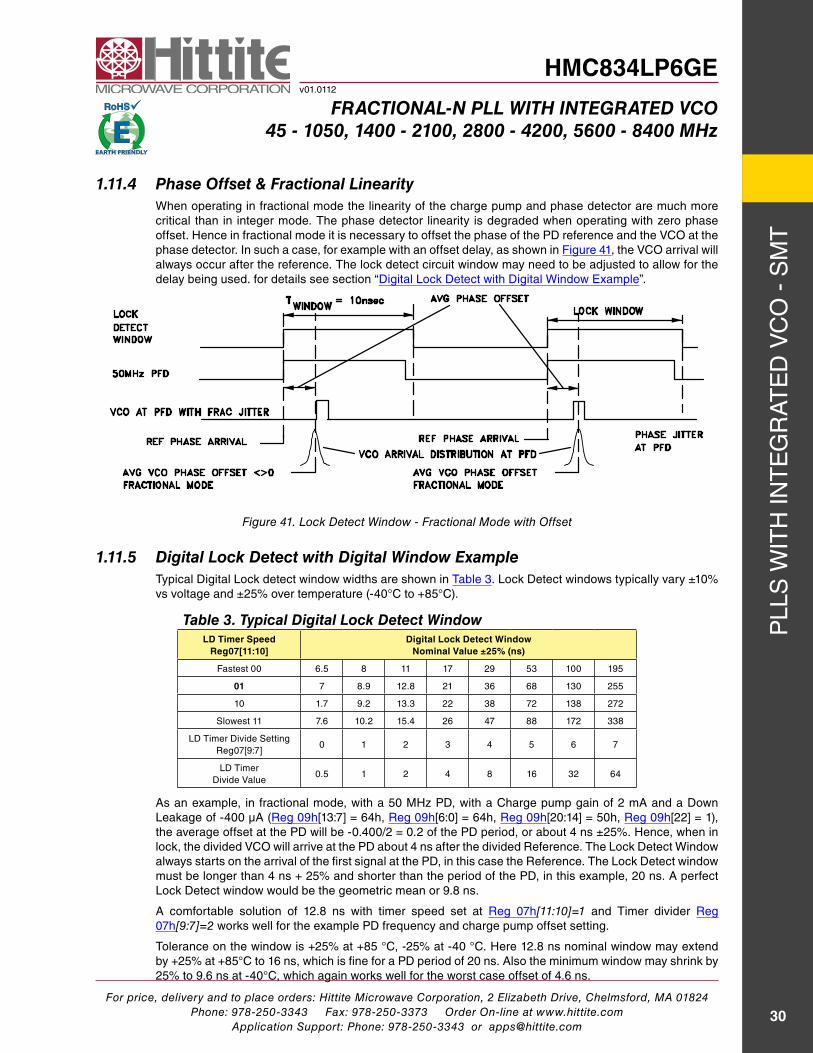
For price, delivery and to place orders: Hittite Microwave Corporation, 2 Elizabeth Drive, Chelmsford, MA 01824Phone: 978-250-3343 Fax: 978-250-3373 Order On-line at www.hittite.com
Application Support: Phone: 978-250-3343 or [email protected]
PLL
s w
ith
int
eg
rat
ed
VC
O -
sM
t
30
HMC834LP6GEv01.0112
Fractional-n Pll with integrated Vco45 - 1050, 1400 - 2100, 2800 - 4200, 5600 - 8400 Mhz
1.11.4 Phase offset & Fractional linearitywhen operating in fractional mode the linearity of the charge pump and phase detector are much more critical than in integer mode. the phase detector linearity is degraded when operating with zero phase offset. hence in fractional mode it is necessary to offset the phase of the Pd reference and the VCO at the phase detector. in such a case, for example with an offset delay, as shown in Figure 41, the VCO arrival will always occur after the reference. the lock detect circuit window may need to be adjusted to allow for the delay being used. for details see section “digital Lock detect with digital window example”.
Figure 41. Lock Detect Window - Fractional Mode with Offset
1.11.5 digital lock detect with digital window exampletypical digital Lock detect window widths are shown in table 3. Lock detect windows typically vary ±10% vs voltage and ±25% over temperature (-40°C to +85°C).
table 3. typical digital lock detect windowLD Timer Speed
Reg07[11:10]Digital Lock Detect Window
Nominal Value ±25% (ns)
Fastest 00 6.5 8 11 17 29 53 100 195
01 7 8.9 12.8 21 36 68 130 255
10 1.7 9.2 13.3 22 38 72 138 272
slowest 11 7.6 10.2 15.4 26 47 88 172 338
Ld timer divide settingreg07[9:7]
0 1 2 3 4 5 6 7
Ld timerdivide Value
0.5 1 2 4 8 16 32 64
as an example, in fractional mode, with a 50 Mhz Pd, with a Charge pump gain of 2 ma and a down Leakage of -400 µa (reg 09h[13:7] = 64h, reg 09h[6:0] = 64h, reg 09h[20:14] = 50h, reg 09h[22] = 1), the average offset at the Pd will be -0.400/2 = 0.2 of the Pd period, or about 4 ns ±25%. hence, when in lock, the divided VCO will arrive at the Pd about 4 ns after the divided reference. the Lock detect window always starts on the arrival of the first signal at the Pd, in this case the reference. the Lock detect window must be longer than 4 ns + 25% and shorter than the period of the Pd, in this example, 20 ns. a perfect Lock detect window would be the geometric mean or 9.8 ns.
a comfortable solution of 12.8 ns with timer speed set at reg 07h[11:10]=1 and timer divider reg 07h[9:7]=2 works well for the example Pd frequency and charge pump offset setting.
tolerance on the window is +25% at +85 °C, -25% at -40 °C. here 12.8 ns nominal window may extend by +25% at +85°C to 16 ns, which is fine for a Pd period of 20 ns. also the minimum window may shrink by 25% to 9.6 ns at -40°C, which again works well for the worst case offset of 4.6 ns.
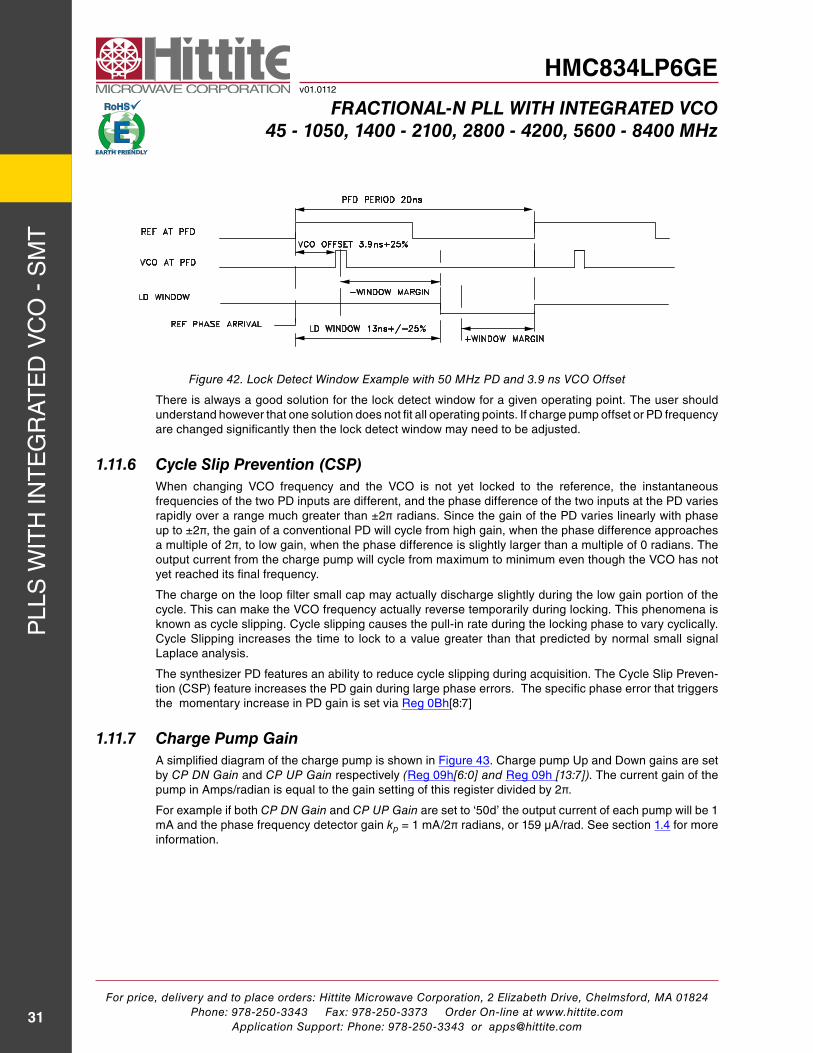
For price, delivery and to place orders: Hittite Microwave Corporation, 2 Elizabeth Drive, Chelmsford, MA 01824Phone: 978-250-3343 Fax: 978-250-3373 Order On-line at www.hittite.com
Application Support: Phone: 978-250-3343 or [email protected]
PLL
s w
ith
int
eg
rat
ed
VC
O -
sM
t
31
HMC834LP6GEv01.0112
Fractional-n Pll with integrated Vco45 - 1050, 1400 - 2100, 2800 - 4200, 5600 - 8400 Mhz
Figure 42. Lock Detect Window Example with 50 MHz PD and 3.9 ns VCO Offset
there is always a good solution for the lock detect window for a given operating point. the user should understand however that one solution does not fit all operating points. if charge pump offset or Pd frequency are changed significantly then the lock detect window may need to be adjusted.
1.11.6 cycle Slip Prevention (cSP)when changing VCO frequency and the VCO is not yet locked to the reference, the instantaneous frequencies of the two Pd inputs are different, and the phase difference of the two inputs at the Pd varies rapidly over a range much greater than ±2π radians. since the gain of the Pd varies linearly with phase up to ±2π, the gain of a conventional Pd will cycle from high gain, when the phase difference approaches a multiple of 2π, to low gain, when the phase difference is slightly larger than a multiple of 0 radians. the output current from the charge pump will cycle from maximum to minimum even though the VCO has not yet reached its final frequency.
the charge on the loop filter small cap may actually discharge slightly during the low gain portion of the cycle. this can make the VCO frequency actually reverse temporarily during locking. this phenomena is known as cycle slipping. Cycle slipping causes the pull-in rate during the locking phase to vary cyclically. Cycle slipping increases the time to lock to a value greater than that predicted by normal small signal Laplace analysis.
the synthesizer Pd features an ability to reduce cycle slipping during acquisition. the Cycle slip Preven-tion (CsP) feature increases the Pd gain during large phase errors. the specific phase error that triggers the momentary increase in Pd gain is set via reg 0Bh[8:7]
1.11.7 charge Pump gaina simplified diagram of the charge pump is shown in Figure 43. Charge pump Up and down gains are set by CP DN Gain and CP UP Gain respectively (reg 09h[6:0] and reg 09h [13:7]). the current gain of the pump in amps/radian is equal to the gain setting of this register divided by 2π.
For example if both CP DN Gain and CP UP Gain are set to ‘50d’ the output current of each pump will be 1 ma and the phase frequency detector gain kp = 1 ma/2π radians, or 159 µa/rad. see section 1.4 for more information.
For price, delivery and to place orders: Hittite Microwave Corporation, 2 Elizabeth Drive, Chelmsford, MA 01824Phone: 978-250-3343 Fax: 978-250-3373 Order On-line at www.hittite.com
Application Support: Phone: 978-250-3343 or [email protected]
PLL
s w
ith
int
eg
rat
ed
VC
O -
sM
t
32
HMC834LP6GEv01.0112
Fractional-n Pll with integrated Vco45 - 1050, 1400 - 2100, 2800 - 4200, 5600 - 8400 Mhz
1.11.8 charge Pump Phase offset - Fractional Modein integer mode, the phase detector operates with zero offset. the divided reference signal and the divided VCO signal arrive at the phase detector inputs at the same time. in fractional mode of operation, charge pump linearity and ultimately, phase noise, is much better if the VCO and reference inputs are operated with a phase offset. a phase offset is implemented by adding a constant dC offset current at the output of the charge pump.
dC offset may be added to the UP or dn switching pumps using reg 09h[21] or reg 09h[22]. the magnitude of the offset is controlled by reg 09h[20:14], and can range from 0 to 635 µa in steps of 5 µa. down offset is highly recommended in fractional mode of operation. integer mode of operation works best with zero offset.
as an example, a Pd comparison of fPD = 50 Mhz (20 ns period) with the main pump gain set at 2 ma, and a down (dn) offset of -385 µa would represent a phase offset of about (-385/2000)*360 = -69 degrees. this is equivalent to the divided VCO arriving 3.8 ns after the reference at the Pd input. it is critical that phase offset be used in fractional mode. normally, down offsets larger than 3 ns are typical.
if the charge pump gain is changed, for example to compensate for changes in VCO sensitivity, it is recommended to change the charge pump offset proportionally to maintain a constant phase offset.
Figure 43. Charge Pump Gain & Offset Control
1.12 Frequency tuninghMC834LP6ge VCO subsystem always operates in fundamental frequency of operation (2800 Mhz to 4200 Mhz). the hMC834LP6ge generates frequencies below its fundamental frequency (45 Mhz to 2800 Mhz) by tuning to the appropriate fundamental frequency and selecting the appropriate Output divider setting (divide by 2/4/6.../60/62) in VCO_reg 02h[5:0]. Conversely the hMC834LP6ge generates frequencies greater than its fundamental frequency (5600 Mhz to 8400 Mhz) by tuning to the appropriate fundamental frequency and enabling the doubler mode (VCO_reg 03h[0] = 1).
the hMC834LP6ge automatically controls frequency tuning in the fundamental band of operation, for more information see “1.2.1 VCO auto-Calibration (autoCal)”.
to tune to frequencies below the fundamental frequency range (<2800 Mhz) it is required to tune the hMC834LP6ge to the appropriate fundamental frequency, then select the appropriate output divider setting (divide by 2/4/6.../60/62) in VCO_reg 02h[5:0]. similarly, to tune to frequencies above the fundamental frequency range (>4200 Mhz) it is required to tune the hMC834LP6ge to the appropriate fundamental frequency, and then enable the doubler mode of operation (VCO_reg 03h[0] = 1).
For price, delivery and to place orders: Hittite Microwave Corporation, 2 Elizabeth Drive, Chelmsford, MA 01824Phone: 978-250-3343 Fax: 978-250-3373 Order On-line at www.hittite.com
Application Support: Phone: 978-250-3343 or [email protected]
PLL
s w
ith
int
eg
rat
ed
VC
O -
sM
t
33
HMC834LP6GEv01.0112
Fractional-n Pll with integrated Vco45 - 1050, 1400 - 2100, 2800 - 4200, 5600 - 8400 Mhz
1.12.1 integer Modethe hMC834LP6ge is capable of operating in integer mode. For integer mode set the following registers
a. disable the Fractional Modulator, reg 06h[11]=0
b. Bypass the Modulator circuit, reg 06h[7]=1
in integer mode the VCO step size is fixed to that of the Pd frequency, fpd. integer mode typically has 3 dB lower phase noise than fractional mode for a given Pd operating frequency. integer mode, however, often requires a lower Pd frequency to meet step size requirements. the fractional mode advantage is that higher Pd frequencies can be used, hence lower phase noise can often be realized in fractional mode. Charge Pump offset should be disabled in integer mode.
1.12.1.1 integer Frequency tuningin integer mode the digital Δ∑ modulator is shut off and the n (reg 03h) divider may be programmed to any integer value in the range 16 to 219-1. to run in integer mode configure reg 06h as described, then program the integer portion of the frequency as explained by (eQ 13), ignoring the fractional part.
a. disable the Fractional Modulator, reg 06h[11] = 0b. Bypass the delta-sigma modulator reg 06h[7] = 1c. to tune to frequencies (<2800 Mhz), select the appropriate output divider value VCO_reg 02h[5:0].d. to tune to frequencies (>4200 Mhz), enable the doubler mode of operation (VCO_reg 03h [0] = 1).
writing to VCO subsystem registers (VCO_reg 02h[5:0] and VCO_reg 03h [0] in this case) is accomplished indirectly through PLL register 5 (reg 05h). More information on communicating with the VCO subsystem through PLL reg 05h is available in “1.19 VCO serial Port interface (sPi)” section.
1.12.2 Fractional Modethe hMC834LP6ge is placed in fractional mode by setting the following registers:
a. enable the Fractional Modulator, reg 06h[11]=1
b. Connect the delta sigma modulator in circuit, reg 06h[7]=0
1.12.2.1 Fractional Frequency tuningthis is a generic example, with the goal of explaining how to program the output frequency. actual variables are dependant upon the reference in use.
the hMC834LP6ge in fractional mode can achieve frequencies at fractional multiples of the reference. the frequency of the hMC834LP6ge, fvco, is given by
fvco = (Nint + Nfrac) = fint + ffrac
fxtal
R (eQ 13)
fout = fvco/ k (eQ 14)
where:
fout is the output frequency after any potential dividers or doublers.
k is 0.5 for doubler, 1 for fundamental, or k = 1,2,4,6,…58,60,62 according to the VCO subsystem type
Nint is the integer division ratio, reg 03h, an integer number between 20 and 524,284
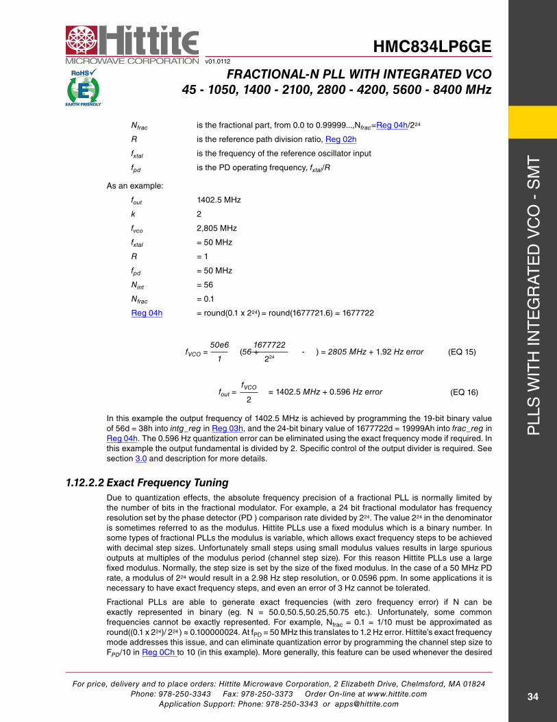
For price, delivery and to place orders: Hittite Microwave Corporation, 2 Elizabeth Drive, Chelmsford, MA 01824Phone: 978-250-3343 Fax: 978-250-3373 Order On-line at www.hittite.com
Application Support: Phone: 978-250-3343 or [email protected]
PLL
s w
ith
int
eg
rat
ed
VC
O -
sM
t
34
HMC834LP6GEv01.0112
Fractional-n Pll with integrated Vco45 - 1050, 1400 - 2100, 2800 - 4200, 5600 - 8400 Mhz
Nfrac is the fractional part, from 0.0 to 0.99999...,nfrac=reg 04h/224
R is the reference path division ratio, reg 02h
fxtal is the frequency of the reference oscillator input
fpd is the Pd operating frequency, fxtal/R
as an example:
fout 1402.5 Mhz
k 2
fvco 2,805 Mhz
fxtal = 50 Mhz
R = 1
fpd = 50 Mhz
Nint = 56
Nfrac = 0.1
reg 04h = round(0.1 x 224) = round(1677721.6) = 1677722
fVCO = (56 + - ) = 2805 MHz + 1.92 Hz error1677722
224
50e6
1(eQ 15)
fout = = 1402.5 MHz + 0.596 Hz errorfVCO
2(eQ 16)
in this example the output frequency of 1402.5 Mhz is achieved by programming the 19-bit binary value of 56d = 38h into intg_reg in reg 03h, and the 24-bit binary value of 1677722d = 19999ah into frac_reg in reg 04h. the 0.596 hz quantization error can be eliminated using the exact frequency mode if required. in this example the output fundamental is divided by 2. specific control of the output divider is required. see section 3.0 and description for more details.
1.12.2.2 exact Frequency tuningdue to quantization effects, the absolute frequency precision of a fractional PLL is normally limited by the number of bits in the fractional modulator. For example, a 24 bit fractional modulator has frequency resolution set by the phase detector (Pd ) comparison rate divided by 224. the value 224 in the denominator is sometimes referred to as the modulus. hittite PLLs use a fixed modulus which is a binary number. in some types of fractional PLLs the modulus is variable, which allows exact frequency steps to be achieved with decimal step sizes. Unfortunately small steps using small modulus values results in large spurious outputs at multiples of the modulus period (channel step size). For this reason hittite PLLs use a large fixed modulus. normally, the step size is set by the size of the fixed modulus. in the case of a 50 Mhz Pd rate, a modulus of 224 would result in a 2.98 hz step resolution, or 0.0596 ppm. in some applications it is necessary to have exact frequency steps, and even an error of 3 hz cannot be tol erated.
Fractional PLLs are able to generate exact frequencies (with zero frequency error) if n can be exactly represented in binary (eg. n = 50.0,50.5,50.25,50.75 etc.). Unfortunately, some common frequencies cannot be exactly represented. For example, nfrac = 0.1 = 1/10 must be approximated as round((0.1 x 224)/ 224 ) ≈ 0.100000024. at fPd = 50 Mhz this translates to 1.2 hz error. hittite’s exact frequency mode addresses this issue, and can eliminate quantization error by programming the channel step size to FPD/10 in reg 0Ch to 10 (in this example). More generally, this feature can be used whenever the desired
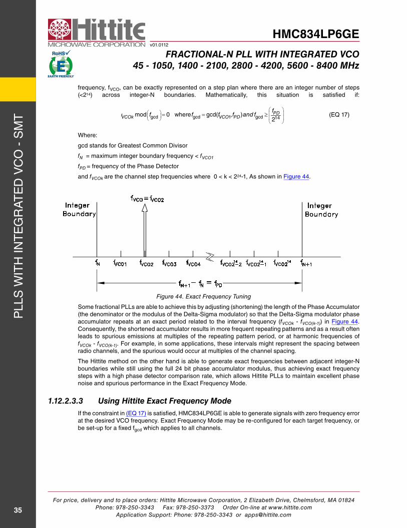
For price, delivery and to place orders: Hittite Microwave Corporation, 2 Elizabeth Drive, Chelmsford, MA 01824Phone: 978-250-3343 Fax: 978-250-3373 Order On-line at www.hittite.com
Application Support: Phone: 978-250-3343 or [email protected]
PLL
s w
ith
int
eg
rat
ed
VC
O -
sM
t
35
HMC834LP6GEv01.0112
Fractional-n Pll with integrated Vco45 - 1050, 1400 - 2100, 2800 - 4200, 5600 - 8400 Mhz
frequency, fVCO, can be exactly represented on a step plan where there are an integer number of steps (<214) across integer-n boundaries. Mathematically, this situation is satisfied if:
gcd gcd gcd1 14mod 0 where gcd( , )
2f PD
PDVCOk VCOf
f f f f and f
= = ≥ (eQ 17)
where:
gcd stands for greatest Common divisor
fN = maximum integer boundary frequency < fVCO1
fPD = frequency of the Phase detector
and fVCOk are the channel step frequencies where 0 < k < 224-1, as shown in Figure 44.
Figure 44. Exact Frequency Tuning
some fractional PLLs are able to achieve this by adjusting (shortening) the length of the Phase accumulator (the denominator or the modulus of the delta-sigma modulator) so that the delta-sigma modulator phase accumulator repeats at an exact period related to the interval frequency (fVCOk - fVCO(k-1)) in Figure 44. Consequently, the shortened accumulator results in more frequent repeating patterns and as a result often leads to spurious emissions at multiples of the repeating pattern period, or at harmonic frequencies of fVCOk - fVCO(k-1). For example, in some applications, these intervals might represent the spacing between radio channels, and the spurious would occur at multiples of the channel spacing.
the hittite method on the other hand is able to generate exact frequencies between adjacent integer-n boundaries while still using the full 24 bit phase accumulator modulus, thus achieving exact frequency steps with a high phase detector comparison rate, which allows hittite PLLs to maintain excellent phase noise and spurious performance in the exact Frequency Mode.
1.12.2.3.3 Using hittite exact Frequency Modeif the constraint in (eQ 17) is satisfied, hMC834LP6ge is able to generate signals with zero frequency error at the desired VCO frequency. exact Frequency Mode may be re-configured for each target frequency, or be set-up for a fixed fgcd which applies to all channels.
For price, delivery and to place orders: Hittite Microwave Corporation, 2 Elizabeth Drive, Chelmsford, MA 01824Phone: 978-250-3343 Fax: 978-250-3373 Order On-line at www.hittite.com
Application Support: Phone: 978-250-3343 or [email protected]
PLL
s w
ith
int
eg
rat
ed
VC
O -
sM
t
36
HMC834LP6GEv01.0112
Fractional-n Pll with integrated Vco45 - 1050, 1400 - 2100, 2800 - 4200, 5600 - 8400 Mhz
1.12.2.4.4 configuring exact Frequency Mode For a Particular Frequency1. Calculate and program the integer register setting reg 03h = NINT = floor(fVCO/fPD), where the
floor function is the rounding down to the nearest integer. then the integer boundary frequency fN = NINT ∙ fPD
2. Calculate and program the exact frequency register value reg 0Ch = fPD/fgcd, where fgcd = gcd(fVCO,fPD)
3. Calculate and program the fractional register setting reg 04h ( )242
ceil NVCOFRAC
PD
f fN
f
−= = , where ceil
is the ceiling function meaning “round up to the nearest integer.”
Example: To configure the HMC834LP6GE for exact frequency mode at fVCO = 2800.2 MHz where Phase Detector (PD) rate fPD = 61.44 MHz Proceed as follows:
Check (eQ 17) to confirm that the exact frequency mode for this fVCO is possible.
( )
gcd gcd 14
66 6 3
gcd 14
gcd( , )2
61.44 10gcd 2800.2 10 ,61.44 10 120 10 37502
PDPDVCO
ff f f and f
f
= ≥
×= × × = × > =
since (eQ 17) is satisfied, the hMC834LP6ge can be configured for exact frequency mode at fVCO = 2800.2 Mhz as follows:
1. nINT = reg 03h = 6
62800.2 10 45 261.44 10
VCO
PD
ffloor floor d Dh
f
×= = =×
2. reg 0Ch = ( ) ( )
6 6
6 6
61.44 10 61.44 10 512 200120000gcd , gcd 2800.2 10 ,61.44 10
PD
PDVCO
fd h
f f× ×= = = =
× ×
3. to program reg 04h, the closest integer-n boundary frequency fN that is less than the desired VCO frequency fVCO must be calculated. fN = fPD ∙ nINT. Using the current example:
( ) ( )6
24 6 624
6
45 61.44 10 2764.8 .
2 2800.2 10 2764.8 102then reg04h 9666560 938000
61.44 10
INTN PD
NVCO
PD
Nf f MHz
f fceil ceil d h
f
= × = × × =
× − ×−= = = =
×
1.12.2.5.5 hittite exact Frequency channel Modeif it is desirable to have multiple, equally spaced, exact frequency channels that fall within the same interval (ie. fN ≤ fVCOk < fN+1) where fVCOk is shown in Figure 44 and 1 ≤ k ≤ 214, it is possible to maintain the same integer-n (reg 03h) and exact frequency register (reg 0Ch) settings and only update the fractional register (reg 04h) setting. the exact Frequency Channel Mode is possible if (eQ 17) is satisfied for at least two equally spaced adjacent frequency channels, i.e. the channel step size.
to configure the hMC834LP6ge for exact Frequency Channel Mode, initially and only at the beginning, integer (reg 03h) and exact frequency (reg 0Ch) registers need to be programmed for the smallest fVCO frequency (fVCO1 in Figure 44), as follows:
1. Calculate and program the integer register setting reg 03h = NINT = floor(fVCO1/fPD), where fVCO1 is shown in Figure 44 and corresponds to minimum channel VCO frequency. then the lower integer boundary frequency is given by fN = NINT ∙ fPD.
2. Calculate and program the exact frequency register value reg 0Ch = fPD/fgcd, where fgcd = gcd((fVCOk+1 - fVCOk),fPD) = greatest common divisor of the desired equidistant channel spacing and the Pd frequency ((fVCOk+1 - fVCOk) and fPD).
For price, delivery and to place orders: Hittite Microwave Corporation, 2 Elizabeth Drive, Chelmsford, MA 01824Phone: 978-250-3343 Fax: 978-250-3373 Order On-line at www.hittite.com
Application Support: Phone: 978-250-3343 or [email protected]
PLL
s w
ith
int
eg
rat
ed
VC
O -
sM
t
37
HMC834LP6GEv01.0112
Fractional-n Pll with integrated Vco45 - 1050, 1400 - 2100, 2800 - 4200, 5600 - 8400 Mhz
then, to switch between various equally spaced intervals (channels) only the fractional register (reg 04h) needs to be programmed to the desired VCO channel frequency fVCOk in the following manner:
reg 04h = ( )242
ceil NVCOkFRAC
PD
f fN
f
−= where fN = floor(fVCO1/fPD), and fVCO1, as shown in Figure 44, represents
the smallest channel VCO frequency that is greater than fN.
Example: To configure the HMC834LP6GE for Exact Frequency Mode for equally spaced intervals of 100 kHz where first channel (Channel 1) = fVCO1 = 2800.200 MHz and Phase Detector (PD) rate fPD = 61.44 MHz proceed as follows:
First check that the exact frequency mode for this fVCO1 = 2800.2 Mhz (Channel 1) and fVCO2 = 2800.2 Mhz + 100 khz = 2800.3 Mhz (Channel 2) is possible.
( )( )
gcd1 gcd1 gcd2 gcd21 214 14
66 6 3
gcd1 14
66 6 3
gcd2 14
gcd( , ) gcd( , )2 2
61.44 10gcd 2800.2 10 ,61.44 10 120 10 37502
61.44 10gcd 2800.3 10 ,61.44 10 20 10 37502
PD PDPD PDVCO VCO
f ff f f and f and f f f and f
f
f
= ≥ = ≥
×= × × = × > =
×= × × = × > =
if (eQ 17) is satisfied for at least two of the equally spaced interval (channel) frequencies fVCO1,fVCO2,fVCO3,...fVCON, as it is above, hittite exact Frequency Channel Mode is possible for all desired channel frequencies, and can be configured as follows:
1. reg 03h = 6
16
2800.2 10 45 261.44 10
VCO
PD
ffloor floor d Dh
f
×= = =×
2. reg 0Ch = ( )( ) ( )
6 6
3 61
61.44 10 61.44 10 3072 0020000gcd 100 10 ,61.44 10gcd ,
PD
PDVCOk VCOk
fd C h
f f f+
× ×= = = =× ×−
where (fVCOk+1 - fVCOk) is the desired channel spacing (100 khz in this example).
3. to program reg 04h the closest integer-n boundary frequency fN that is less than the smallest channel VCO frequency fVCO1 must be calculated. fN = floor(fVCO1/fPD). Using the current example: 6
66
2800.2 10 45 61.44 10 2764.861.44 10N PDf f floor MHz
×= × = × × =×
then reg 04h
( )
( )
241
1
24 6 6
6
2 for channel 1 where 2800.2
2 2800.2 10 2764.8 109666560 938000
61.44 10
NVCOVCO
PD
f fceil f MHz
f
ceil d h
−= =
× − ×= = =
×
4. to change from channel 1 (fVCO1 = 2800.2 Mhz) to channel 2 (fVCO2 = 2800.3 Mhz), only reg 04h needs to be programmed, as long as all of the desired exact frequencies fVCOk (Figure 44) fall between the same integer-n boundaries (fN < fVCOk < fN+1). in that case reg 04h =
( )24 6 6
6
2 2800.3 10 2764.8 109693867 93
61.44 10ceil d EAABh
× − ×= =
×, and so on.
For price, delivery and to place orders: Hittite Microwave Corporation, 2 Elizabeth Drive, Chelmsford, MA 01824Phone: 978-250-3343 Fax: 978-250-3373 Order On-line at www.hittite.com
Application Support: Phone: 978-250-3343 or [email protected]
PLL
s w
ith
int
eg
rat
ed
VC
O -
sM
t
38
HMC834LP6GEv01.0112
Fractional-n Pll with integrated Vco45 - 1050, 1400 - 2100, 2800 - 4200, 5600 - 8400 Mhz
1.12.2.6 Seed register & autoSeed Modethe start phase of the fractional modulator digital phase accumulator (dPa) may be set to one of four possible default values via the seed register reg 06h[1:0]. if autoseed reg 06h[8] is set, then the hMC834LP6ge will automatically reload the start phase into the dPa every time a new fractional frequency is selected. if autoseed is not set, then the hMC834LP6ge will start new fractional frequencies with the last value left in the dPa from the last frequency. hence the start phase will effectively be random. Certain zero or binary seed values may cause spurious energy correlation at specific frequencies. Correlated spurs are advantageous only in very special cases where the spurious are known to be far out of band and are removed in the loop filter. For most cases a random, or non zero, non-binary start seed is recommended. Further, since the autoseed always starts the accumulators at the same place, performance is repeatable
if autoseed is used. reg 06h[1:0]=2 is recommended.
1.13 Soft reset & Power-on resetthe hMC834LP6ge features a hardware Power on reset (POr). all chip registers will be reset to default states approximately 250 µs after power up.
the PLL subsystem sPi registers may also be soft reset by an sPi write to register rst_swrst (reg 00h). note that the soft reset does not clear the sPi mode of operation referred to in section 1.17.2. it should be noted that the VCO subsystem is not affected by the PLL soft reset, the VCO subsystem registers can only be reset by removing the power supply.
NOTE: if external power supplies or regulators have rise times slower than 250 µs, then it is advised to write to the SPI reset register (reg 00h[5]=1) immediately after power up, before any other SPI activity. This will ensure starting from a known state.
1.14 Power down Mode note that the VCO subsystem is not affected by the Cen or soft reset. hence device power down is a two step process. First power down the VCO by writing 0 to VCO register 1 via reg 05h and then power down the PLL by pulling Cen pin 17 low (assuming no sPi overrides (reg 01h[0]=1)). this will result in all analog functions and internal clocks disabled. Current consumption will typically drop below 10 µa in Power down state. the serial port will still respond to normal communication in Power down mode.
it is possible to ignore the Cen pin, by clearing rst_chipen_pin_select (reg 01h[0]=0). Control of Power down Mode then comes from the serial port register rst_chipen_from_spi, reg 01h[1] .
it is also possible to leave various blocks on when in Power down (see reg 01h), including:
a. internal Bias reference sources reg 01h[2]b. Pd Block reg 01h[3]c. CP Block reg 01h[4]d. reference Path Buffer reg 01h[5]e. VCO Path buffer reg 01h[6]f. digital i/O test pads reg 01h[7]
to turn off the VCO rF buffer but leave the VCO running and the PLL locked write reg 05h = 2a98(manual select) then write reg 05h = 0d88(disable VCO rF buffer) to re-enable the rF buffer write reg
05h=0F88(enable VCO rF buffer)
1.15 chip identificationPLL subsystem version information may be read by reading the content of read only register, chip_id in reg 00h. it is not possible to read the VCO subsystem version.
For price, delivery and to place orders: Hittite Microwave Corporation, 2 Elizabeth Drive, Chelmsford, MA 01824Phone: 978-250-3343 Fax: 978-250-3373 Order On-line at www.hittite.com
Application Support: Phone: 978-250-3343 or [email protected]
PLL
s w
ith
int
eg
rat
ed
VC
O -
sM
t
39
HMC834LP6GEv01.0112
Fractional-n Pll with integrated Vco45 - 1050, 1400 - 2100, 2800 - 4200, 5600 - 8400 Mhz
1.16 general Purpose output (gPo) Pin the PLL shares the Ld_sdO (Lock-detect/serial data Out) pin to perform various functions. while the pin is most commonly used to read back registers from chip via the sPi, it is also capable of exporting a variety of interesting signals and real time test waveforms (including Lock detect). it is driven by a tri-state CMOs driver with ~200 Ω rout. it has logic associated with it to dynamically select whether the driver is enabled, and to decide which data to export from the chip.
in its default configuration, after power-on-reset, the output driver is disabled, and only drives during appropriately addressed sPi reads. this allows it to share the output with other devices on the same bus.
depending on the sPi mode, the read section of sPi cycle is recognized differently
hMC sPi Mode: the driver is enabled during the last 24 bits of sPi read cycle (not during write cycles).
Open sPi Mode: the driver is enabled if the chip is addressed - ie. the last 3 bits of sPi cycle = ‘000’b before the rising edge of sen (note a).
to monitor any of the gPO signals, including Lock detect, set reg 0Fh[7] = 1 to keep the sdO driver always on. this stops the LdO driver from tri-stating and means that the sdO line cannot be shared with other devices.
the chip will naturally switch away from the gPO data and export the sdO during an sPi read (note B). to prevent this automatic data selection, and always select the gPO signal, set “Prevent autoMux of sdO” (reg 0Fh[6] = 1). the phase noise performance at this output is poor and uncharacterized. also, the gPO output should not be toggling during normal operation. Otherwise the spectral performance may degrade.
note that there are additional controls available, which may be helpful if sharing the bus with other devices:
• to allow the driver to be active (subject to the conditions above) even when the chip is disabled - set reg 01h[7] = 0.
• to disable the driver completely, set reg 08h[5] = 0 (it takes precedence over all else).
• to disable either the pull-up or pull-down sections of the driver, reg 0Fh[8] = 1 or reg 0Fh[9] = 1 respectively.
Note A: If SEN rises before SCK has clocked in an ‘invalid’ (non-zero) chip -address, the HMC834LP6GE will start to drive the bus.
Note B: In Open Mode, the active portion of the read is defined between the 1st SCK rising edge after SEN, to the next rising edge of SEN.
example scenarios:
• drive sdO during reads, tri-state otherwise (to allow bus-sharing)• no action required.
• drive sdO during reads, Lock detect otherwise• set gPO select reg 0Fh[4:0] = ‘00001’ (which is default)• set “Prevent gPO driver disable” (reg 0Fh[7] = 1)
• always drive Lock detect• set “ Prevent autoMux of sdO” reg 0Fh[6] = 1• set gPO select reg 0Fh[4:0]= 00001 (which is default)• set “Prevent gPO driver disable” (reg 0Fh[7] = 1))
the signals available on the gPO are selected by changing “gPO select”, reg 0Fh[4:0].
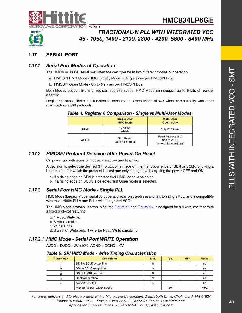
For price, delivery and to place orders: Hittite Microwave Corporation, 2 Elizabeth Drive, Chelmsford, MA 01824Phone: 978-250-3343 Fax: 978-250-3373 Order On-line at www.hittite.com
Application Support: Phone: 978-250-3343 or [email protected]
PLL
s w
ith
int
eg
rat
ed
VC
O -
sM
t
40
HMC834LP6GEv01.0112
Fractional-n Pll with integrated Vco45 - 1050, 1400 - 2100, 2800 - 4200, 5600 - 8400 Mhz
1.17 SERIAL PORT
1.17.1 Serial Port Modes of operationthe hMC834LP6ge serial port interface can operate in two different modes of operation.
a. hMCsPi hMC Mode (hMC Legacy Mode) - single slave per hMCsPi Bus
b. hMCsPi Open Mode - Up to 8 slaves per hMCsPi Bus.
Both Modes support 5-bits of register address space. hMC Mode can support up to 6 bits of register address.
register 0 has a dedicated function in each mode. Open Mode allows wider compatibility with other manufacturers sPi protocols.
table 4. register 0 comparison - Single vs Multi-User ModesSingle UserHMC Mode
Multi-UserOpen Mode
readChip id24-bits
Chip id 24-bits
WRITEsoft reset,
general strobes
read address [4:0]soft reset [5]
general strobes [23:6]
1.17.2 hMcSPi Protocol decision after Power-on resetOn power up both types of modes are active and listening.
a decision to select the desired sPi protocol is made on the first occurrence of sen or sCLK following a hard reset, after which the protocol is fixed and only changeable by cycling the power OFF and On.
a. if a rising edge on sen is detected first hMC Mode is selected.b. if a rising edge on sCLK is detected first Open mode is selected.
1.17.3 Serial Port hMc Mode - Single PllhMC Mode (Legacy Mode) serial port operation can only address and talk to a single PLL, and is compatible with most hittite PLLs and PLLs with integrated VCOs.
the hMC Mode protocol, shown in figures Figure 45 and Figure 46, is designed for a 4 wire interface with a fixed protocol featuring
a. 1 read/write bitb. 6 address bitsc. 24 data bitsd. 3 wire for write only, 4 wire for read/write capability
1.17.3.1 hMc Mode - Serial Port write operationaVdd = dVdd = 3V ±10%, agnd = dgnd = 0V
table 5. SPi hMc Mode - write timing characteristicsParameter Conditions Min. Typ. Max Units
t1 sen to sCLK setup time 8 ns
t2 sdi to sCLK setup time 3 ns
t3 sCLK to sdi hold time 3 ns
t4 sen low duration 20 ns
t5 sCK to sen fall 10 ns
Max serial port Clock speed 50 Mhz
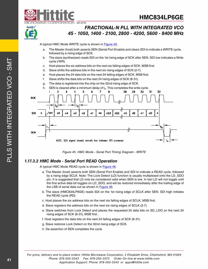
For price, delivery and to place orders: Hittite Microwave Corporation, 2 Elizabeth Drive, Chelmsford, MA 01824Phone: 978-250-3343 Fax: 978-250-3373 Order On-line at www.hittite.com
Application Support: Phone: 978-250-3343 or [email protected]
PLL
s w
ith
int
eg
rat
ed
VC
O -
sM
t
41
HMC834LP6GEv01.0112
Fractional-n Pll with integrated Vco45 - 1050, 1400 - 2100, 2800 - 4200, 5600 - 8400 Mhz
a typical hMC Mode write cycle is shown in Figure 45.
a. the Master (host) both asserts sen (serial Port enable) and clears sdi to indicate a write cycle, followed by a rising edge of sCK.
b. the slave (synthesizer) reads sdi on the 1st rising edge of sCK after sen. sdi low indi cates a write cycle (/wr).
c. host places the six address bits on the next six falling edges of sCK, MsB first.d. slave shifts the address bits in the next six rising edges of sCK (2-7).e. host places the 24 data bits on the next 24 falling edges of sCK, MsB first.f. slave shifts the data bits on the next 24 rising edges of sCK (8-31).g. the data is registered into the chip on the 32nd rising edge of sCK.h. sen is cleared after a minimum delay of t5. this completes the write cycle.
Figure 45. HMC Mode - Serial Port Timing Diagram - WRITE
1.17.3.2 hMc Mode - Serial Port read operationa typical hMC Mode read cycle is shown in Figure 46.
a. the Master (host) asserts both sen (serial Port enable) and sdi to indicate a read cycle, followed by a rising edge sCLK. note: the Lock detect (Ld) function is usually multiplexed onto the Ld_sdO pin. it is suggested that Ld only be considered valid when sen is low. in fact Ld will not toggle until the first active data bit toggles on Ld_sdO, and will be restored immediately after the trailing edge of the LsB of serial data out as shown in Figure 46.
b. the slave (hMC834LP6ge) reads sdi on the 1st rising edge of sCLK after sen. sdi high initiates the read cycle (rd)
c. host places the six address bits on the next six falling edges of sCLK, MsB first.
d. slave registers the address bits on the next six rising edges of sCLK (2-7).
e. slave switches from Lock detect and places the requested 24 data bits on sd_LdO on the next 24 rising edges of sCK (8-31), MsB first .
f. host registers the data bits on the next 24 falling edges of sCK (8-31).
g. slave restores Lock detect on the 32nd rising edge of sCK.
h. de-assertion of sen completes the cycle
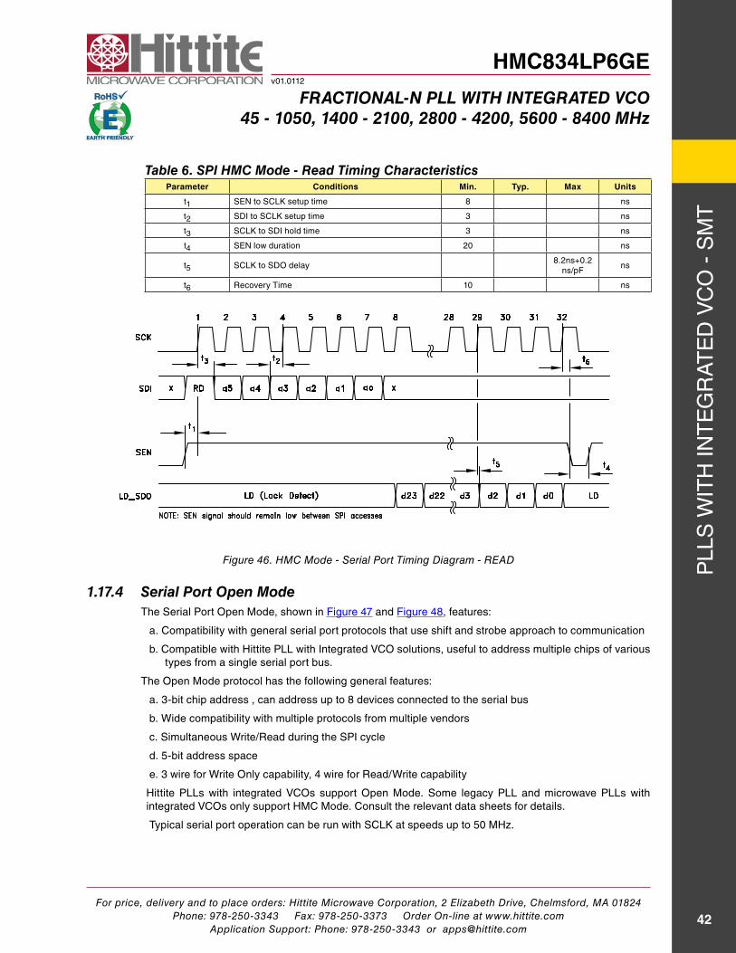
For price, delivery and to place orders: Hittite Microwave Corporation, 2 Elizabeth Drive, Chelmsford, MA 01824Phone: 978-250-3343 Fax: 978-250-3373 Order On-line at www.hittite.com
Application Support: Phone: 978-250-3343 or [email protected]
PLL
s w
ith
int
eg
rat
ed
VC
O -
sM
t
42
HMC834LP6GEv01.0112
Fractional-n Pll with integrated Vco45 - 1050, 1400 - 2100, 2800 - 4200, 5600 - 8400 Mhz
table 6. SPi hMc Mode - read timing characteristicsParameter Conditions Min. Typ. Max Units
t1 sen to sCLK setup time 8 ns
t2 sdi to sCLK setup time 3 ns
t3 sCLK to sdi hold time 3 ns
t4 sen low duration 20 ns
t5 sCLK to sdO delay8.2ns+0.2
ns/pFns
t6 recovery time 10 ns
Figure 46. HMC Mode - Serial Port Timing Diagram - READ
1.17.4 Serial Port open Modethe serial Port Open Mode, shown in Figure 47 and Figure 48, features:
a. Compatibility with general serial port protocols that use shift and strobe approach to communication
b. Compatible with hittite PLL with integrated VCO solutions, useful to address multiple chips of various types from a single serial port bus.
the Open Mode protocol has the following general features:
a. 3-bit chip address , can address up to 8 devices connected to the serial bus
b. wide compatibility with multiple protocols from multiple vendors
c. simultaneous write/read during the sPi cycle
d. 5-bit address space
e. 3 wire for write Only capability, 4 wire for read/write capability
hittite PLLs with integrated VCOs support Open Mode. some legacy PLL and microwave PLLs with integrated VCOs only support hMC Mode. Consult the relevant data sheets for details.
typical serial port operation can be run with sCLK at speeds up to 50 Mhz.
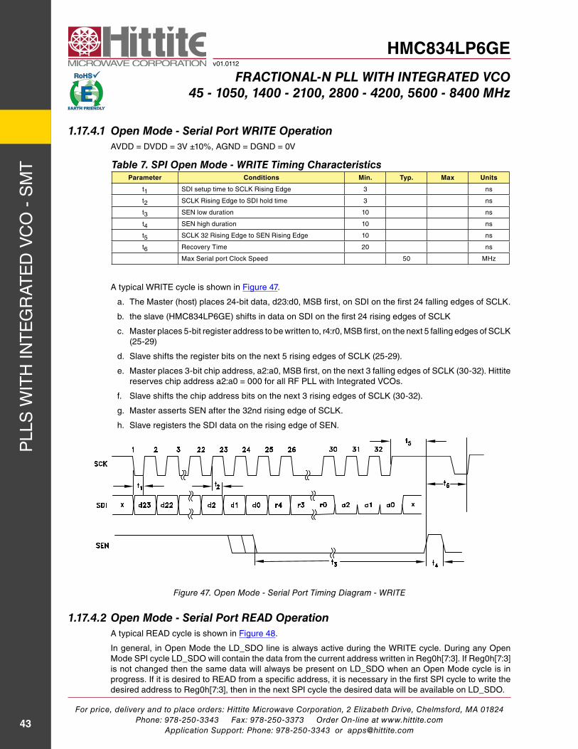
For price, delivery and to place orders: Hittite Microwave Corporation, 2 Elizabeth Drive, Chelmsford, MA 01824Phone: 978-250-3343 Fax: 978-250-3373 Order On-line at www.hittite.com
Application Support: Phone: 978-250-3343 or [email protected]
PLL
s w
ith
int
eg
rat
ed
VC
O -
sM
t
43
HMC834LP6GEv01.0112
Fractional-n Pll with integrated Vco45 - 1050, 1400 - 2100, 2800 - 4200, 5600 - 8400 Mhz
1.17.4.1 open Mode - Serial Port write operationaVdd = dVdd = 3V ±10%, agnd = dgnd = 0V
table 7. SPi open Mode - write timing characteristicsParameter Conditions Min. Typ. Max Units
t1 sdi setup time to sCLK rising edge 3 ns
t2 sCLK rising edge to sdi hold time 3 ns
t3 sen low duration 10 ns
t4 sen high duration 10 ns
t5 sCLK 32 rising edge to sen rising edge 10 ns
t6 recovery time 20 ns
Max serial port Clock speed 50 Mhz
a typical write cycle is shown in Figure 47.
a. the Master (host) places 24-bit data, d23:d0, MsB first, on sdi on the first 24 falling edges of sCLK.
b. the slave (hMC834LP6ge) shifts in data on sdi on the first 24 rising edges of sCLK
c. Master places 5-bit register address to be written to, r4:r0, MsB first, on the next 5 falling edges of sCLK (25-29)
d. slave shifts the register bits on the next 5 rising edges of sCLK (25-29).
e. Master places 3-bit chip address, a2:a0, MsB first, on the next 3 falling edges of sCLK (30-32). hittite reserves chip address a2:a0 = 000 for all rF PLL with integrated VCOs.
f. slave shifts the chip address bits on the next 3 rising edges of sCLK (30-32).
g. Master asserts sen after the 32nd rising edge of sCLK.
h. slave registers the sdi data on the rising edge of sen.
Figure 47. Open Mode - Serial Port Timing Diagram - WRITE
1.17.4.2 open Mode - Serial Port read operationa typical read cycle is shown in Figure 48.
in general, in Open Mode the Ld_sdO line is always active during the write cycle. during any Open Mode sPi cycle Ld_sdO will contain the data from the current address written in reg0h[7:3]. if reg0h[7:3] is not changed then the same data will always be present on Ld_sdO when an Open Mode cycle is in progress. if it is desired to read from a specific address, it is necessary in the first sPi cycle to write the desired address to reg0h[7:3], then in the next sPi cycle the desired data will be available on Ld_sdO.
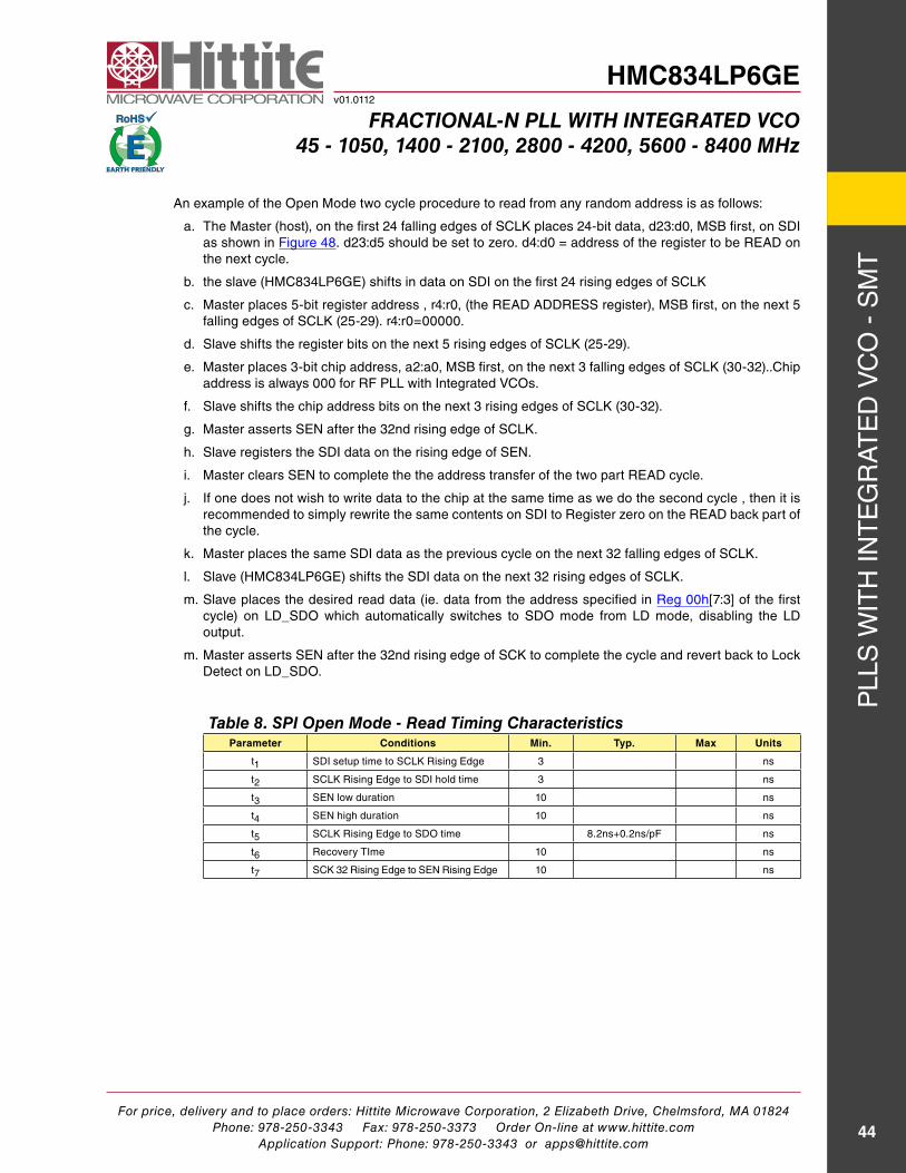
For price, delivery and to place orders: Hittite Microwave Corporation, 2 Elizabeth Drive, Chelmsford, MA 01824Phone: 978-250-3343 Fax: 978-250-3373 Order On-line at www.hittite.com
Application Support: Phone: 978-250-3343 or [email protected]
PLL
s w
ith
int
eg
rat
ed
VC
O -
sM
t
44
HMC834LP6GEv01.0112
Fractional-n Pll with integrated Vco45 - 1050, 1400 - 2100, 2800 - 4200, 5600 - 8400 Mhz
an example of the Open Mode two cycle procedure to read from any random address is as follows:
a. the Master (host), on the first 24 falling edges of sCLK places 24-bit data, d23:d0, MsB first, on sdi as shown in Figure 48. d23:d5 should be set to zero. d4:d0 = address of the register to be read on the next cycle.
b. the slave (hMC834LP6ge) shifts in data on sdi on the first 24 rising edges of sCLK
c. Master places 5-bit register address , r4:r0, (the read address register), MsB first, on the next 5 falling edges of sCLK (25-29). r4:r0=00000.
d. slave shifts the register bits on the next 5 rising edges of sCLK (25-29).
e. Master places 3-bit chip address, a2:a0, MsB first, on the next 3 falling edges of sCLK (30-32)..Chip address is always 000 for rF PLL with integrated VCOs.
f. slave shifts the chip address bits on the next 3 rising edges of sCLK (30-32).
g. Master asserts sen after the 32nd rising edge of sCLK.
h. slave registers the sdi data on the rising edge of sen.
i. Master clears sen to complete the the address transfer of the two part read cycle.
j. if one does not wish to write data to the chip at the same time as we do the second cycle , then it is recommended to simply rewrite the same contents on sdi to register zero on the read back part of the cycle.
k. Master places the same sdi data as the previous cycle on the next 32 falling edges of sCLK.
l. slave (hMC834LP6ge) shifts the sdi data on the next 32 rising edges of sCLK.
m. slave places the desired read data (ie. data from the address specified in reg 00h[7:3] of the first cycle) on Ld_sdO which automatically switches to sdO mode from Ld mode, disabling the Ld output.
m. Master asserts sen after the 32nd rising edge of sCK to complete the cycle and revert back to Lock detect on Ld_sdO.
table 8. SPi open Mode - read timing characteristicsParameter Conditions Min. Typ. Max Units
t1 sdi setup time to sCLK rising edge 3 ns
t2 sCLK rising edge to sdi hold time 3 ns
t3 sen low duration 10 ns
t4 sen high duration 10 ns
t5 sCLK rising edge to sdO time 8.2ns+0.2ns/pF ns
t6 recovery time 10 ns
t7 sCK 32 rising edge to sen rising edge 10 ns
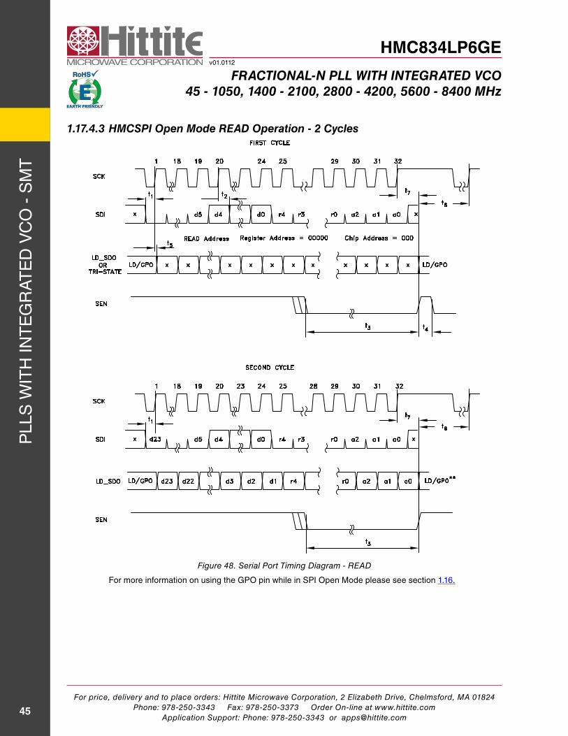
For price, delivery and to place orders: Hittite Microwave Corporation, 2 Elizabeth Drive, Chelmsford, MA 01824Phone: 978-250-3343 Fax: 978-250-3373 Order On-line at www.hittite.com
Application Support: Phone: 978-250-3343 or [email protected]
PLL
s w
ith
int
eg
rat
ed
VC
O -
sM
t
45
HMC834LP6GEv01.0112
Fractional-n Pll with integrated Vco45 - 1050, 1400 - 2100, 2800 - 4200, 5600 - 8400 Mhz
1.17.4.3 hMcSPi open Mode read operation - 2 cycles
Figure 48. Serial Port Timing Diagram - READ
For more information on using the gPO pin while in sPi Open Mode please see section 1.16.
For price, delivery and to place orders: Hittite Microwave Corporation, 2 Elizabeth Drive, Chelmsford, MA 01824Phone: 978-250-3343 Fax: 978-250-3373 Order On-line at www.hittite.com
Application Support: Phone: 978-250-3343 or [email protected]
PLL
s w
ith
int
eg
rat
ed
VC
O -
sM
t
46
HMC834LP6GEv01.0112
Fractional-n Pll with integrated Vco45 - 1050, 1400 - 2100, 2800 - 4200, 5600 - 8400 Mhz
1.18 configuration at Start-Upto configure the PLL after power up, follow the instructions below:
1. Configure the reference divider (write to reg 02h), if required.
2. Configure the delta-sigma modulator (write to reg 06h). • Configuration involves selecting the mode of the delta-sigma modulator (Mode a or Mode B),
selection of the delta-sigma modulator seed value, and configuration of the delta-sigma modulator clock scheme. it is recommended to use the values found in the hittite PLL evaluation board control software register files.
3. Configure the charge pump current and charge pump offset current (write to reg 09h)
4. Configure the VCO subsystem (write to reg 05h, for more information see section 1.19, and “3.0 VCO subsystem register Map”. detailed writes to the VCO subsystem via PLL reg 05h at start-up are available in the register setting Files found in the hittite PLL evaluation software received with a product evaluation kit or downloaded from www.hittite.com.
5. Program the frequency of operation• Program the integer part (write to reg 03h)• Program the fractional part (write to reg 04h)
6. Configure the VCO output divider/doubler, if needed in the VCO subsystem via PLL reg 05h.
Once the hMC834LP6ge is configured after startup, in most cases the user only needs to change frequencies by writing to reg 03h integer register, reg 04h fractional register, and reg 05h to change the VCO output divider or doubler setting if needed, and possibly adjust the charge pump settings by writing to reg 09h.
For detailed and most up-to-date start-up configuration please refer to the appropriate register setting Files found in the hittite PLL evaluation software received with a product evaluation kit or downloaded from www.hittite.com.
1.19 Vco Serial Port interface (SPi)the hMC834LP6ge communicates with the internal VCO subsystem via an internal 16 bit VCO serial Port, (e.g. see Figure 29). the internal serial port is used to control the step tuned VCO and other VCO subsystem functions, such as rF output divider / doubler control and rF buffer enable.
note that the internal VCO subsystem sPi (VsPi) runs at the rate of the autoCal FsM clock, TFSM, (section 1.2.1) where the FsM clock frequency cannot be greater than 50 Mhz. the VsPi clock rate is set by reg 0ah[14:13].
writes to the VCO’s control registers are handled indirectly, via writes to reg 05h of the PLL. a write to PLL reg 05h causes the PLL subsystem to forward the packet, MsB first, across its internal serial link to the VCO subsystem, where it is interpreted.
the VCO serial port has the capability to communicate with multiple subsystems inside the iC. For this reason each subsystem has a subsystem id, reg 05h[2:0].
each subsystem has multiple registers to control the functions internal to the subsystem, which may be different from one subsystem to the next. hence each subsystem has internal register addresses bits (reg 05h[6:3])
Finally the data required to configure each register within the VCO subsystem is contained in reg 05h[15:7].
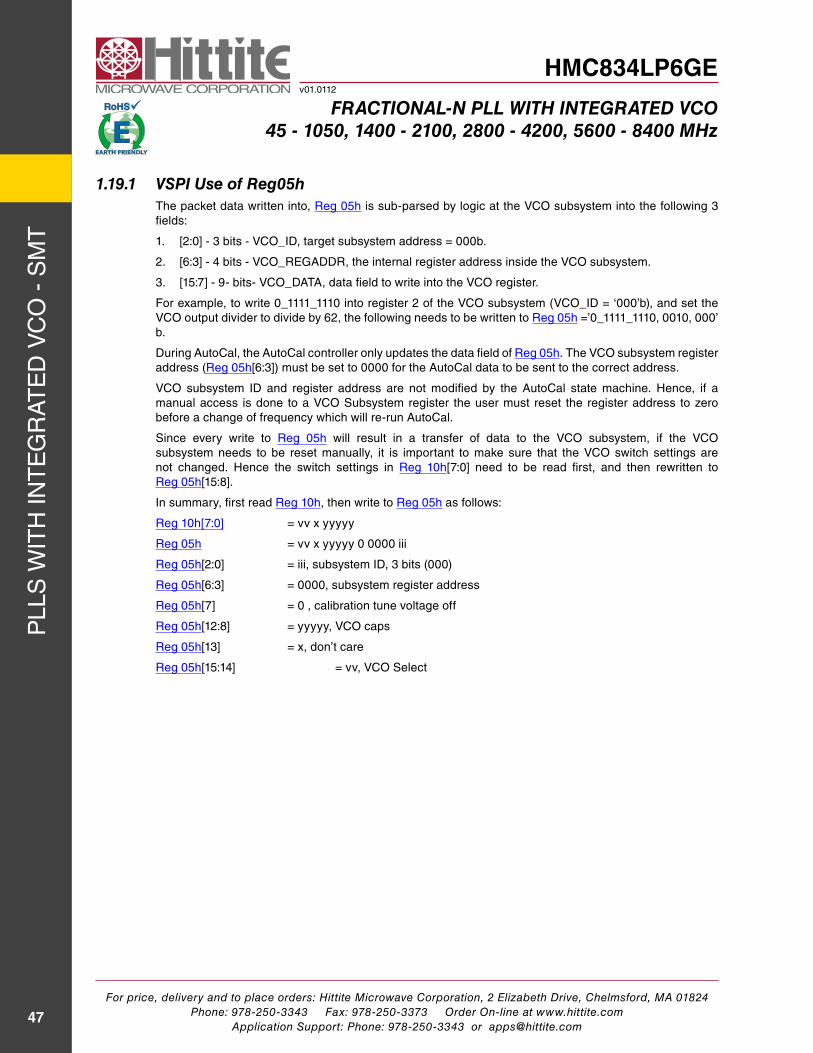
For price, delivery and to place orders: Hittite Microwave Corporation, 2 Elizabeth Drive, Chelmsford, MA 01824Phone: 978-250-3343 Fax: 978-250-3373 Order On-line at www.hittite.com
Application Support: Phone: 978-250-3343 or [email protected]
PLL
s w
ith
int
eg
rat
ed
VC
O -
sM
t
47
HMC834LP6GEv01.0112
Fractional-n Pll with integrated Vco45 - 1050, 1400 - 2100, 2800 - 4200, 5600 - 8400 Mhz
1.19.1 VSPi Use of reg05hthe packet data written into, reg 05h is sub-parsed by logic at the VCO subsystem into the following 3 fields:
1. [2:0] - 3 bits - VCO_id, target subsystem address = 000b.
2. [6:3] - 4 bits - VCO_regaddr, the internal register address inside the VCO subsystem.
3. [15:7] - 9- bits- VCO_data, data field to write into the VCO register.
For example, to write 0_1111_1110 into register 2 of the VCO subsystem (VCO_id = ‘000’b), and set the VCO output divider to divide by 62, the following needs to be written to reg 05h =’0_1111_1110, 0010, 000’ b.
during autoCal, the autoCal controller only updates the data field of reg 05h. the VCO subsystem register address (reg 05h[6:3]) must be set to 0000 for the autoCal data to be sent to the correct address.
VCO subsystem id and register address are not modified by the autoCal state machine. hence, if a manual access is done to a VCO subsystem register the user must reset the register address to zero before a change of frequency which will re-run autoCal.
since every write to reg 05h will result in a transfer of data to the VCO subsystem, if the VCO subsystem needs to be reset manually, it is important to make sure that the VCO switch settings are not changed. hence the switch settings in reg 10h[7:0] need to be read first, and then rewritten to reg 05h[15:8].
in summary, first read reg 10h, then write to reg 05h as follows:
reg 10h[7:0] = vv x yyyyy
reg 05h = vv x yyyyy 0 0000 iii
reg 05h[2:0] = iii, subsystem id, 3 bits (000)
reg 05h[6:3] = 0000, subsystem register address
reg 05h[7] = 0 , calibration tune voltage off
reg 05h[12:8] = yyyyy, VCO caps
reg 05h[13] = x, don’t care
reg 05h[15:14] = vv, VCO select
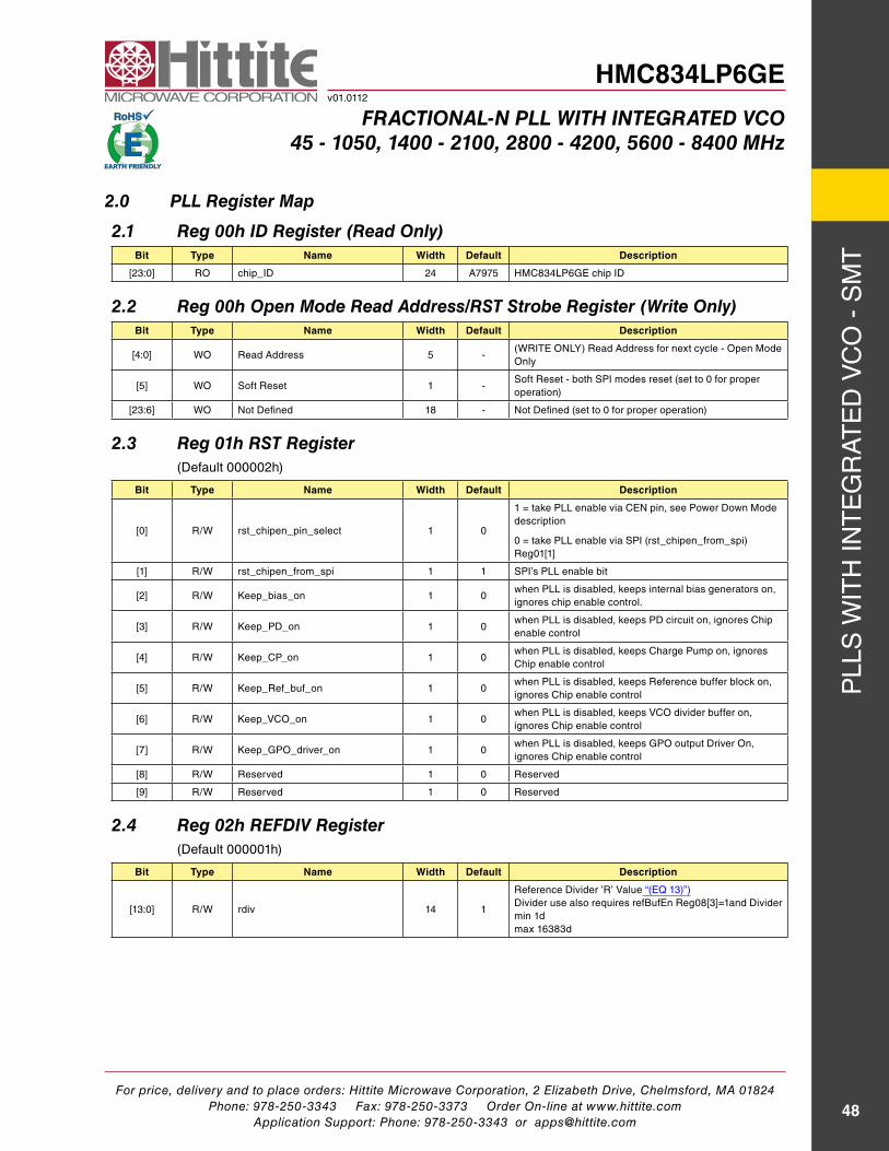
For price, delivery and to place orders: Hittite Microwave Corporation, 2 Elizabeth Drive, Chelmsford, MA 01824Phone: 978-250-3343 Fax: 978-250-3373 Order On-line at www.hittite.com
Application Support: Phone: 978-250-3343 or [email protected]
PLL
s w
ith
int
eg
rat
ed
VC
O -
sM
t
48
HMC834LP6GEv01.0112
Fractional-n Pll with integrated Vco45 - 1050, 1400 - 2100, 2800 - 4200, 5600 - 8400 Mhz
2.0 Pll register Map
2.1 reg 00h id register (read only)Bit Type Name Width Default Description
[23:0] rO chip_id 24 a7975 hMC834LP6ge chip id
2.2 reg 00h open Mode read address/rSt Strobe register (write only)Bit Type Name Width Default Description
[4:0] wO read address 5 -(write OnLY) read address for next cycle - Open Mode Only
[5] wO soft reset 1 -soft reset - both sPi modes reset (set to 0 for proper operation)
[23:6] wO not defined 18 - not defined (set to 0 for proper operation)
2.3 reg 01h rSt register (default 000002h)
Bit Type Name Width Default Description
[0] r/w rst_chipen_pin_select 1 0
1 = take PLL enable via Cen pin, see Power down Mode description
0 = take PLL enable via sPi (rst_chipen_from_spi) reg01[1]
[1] r/w rst_chipen_from_spi 1 1 sPi’s PLL enable bit
[2] r/w Keep_bias_on 1 0when PLL is disabled, keeps internal bias generators on, ignores chip enable control.
[3] r/w Keep_Pd_on 1 0when PLL is disabled, keeps Pd circuit on, ignores Chip enable control
[4] r/w Keep_CP_on 1 0when PLL is disabled, keeps Charge Pump on, ignores Chip enable control
[5] r/w Keep_ref_buf_on 1 0when PLL is disabled, keeps reference buffer block on, ignores Chip enable control
[6] r/w Keep_VCO_on 1 0when PLL is disabled, keeps VCO divider buffer on, ignores Chip enable control
[7] r/w Keep_gPO_driver_on 1 0when PLL is disabled, keeps gPO output driver On, ignores Chip enable control
[8] r/w reserved 1 0 reserved
[9] r/w reserved 1 0 reserved
2.4 reg 02h reFdiV register (default 000001h)
Bit Type Name Width Default Description
[13:0] r/w rdiv 14 1
reference divider ’r’ Value “(eQ 13)”)divider use also requires refBufen reg08[3]=1and dividermin 1dmax 16383d
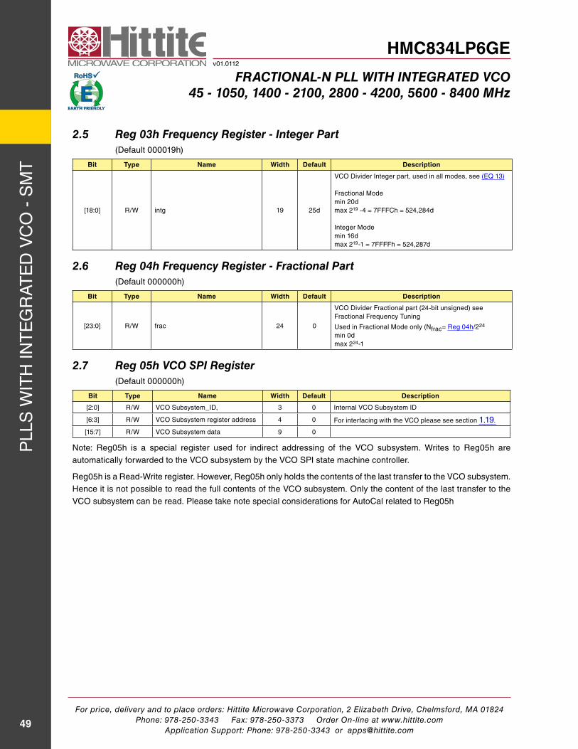
For price, delivery and to place orders: Hittite Microwave Corporation, 2 Elizabeth Drive, Chelmsford, MA 01824Phone: 978-250-3343 Fax: 978-250-3373 Order On-line at www.hittite.com
Application Support: Phone: 978-250-3343 or [email protected]
PLL
s w
ith
int
eg
rat
ed
VC
O -
sM
t
49
HMC834LP6GEv01.0112
Fractional-n Pll with integrated Vco45 - 1050, 1400 - 2100, 2800 - 4200, 5600 - 8400 Mhz
2.5 reg 03h Frequency register - integer Part (default 000019h)
Bit Type Name Width Default Description
[18:0] r/w intg 19 25d
VCO divider integer part, used in all modes, see (eQ 13)
Fractional Modemin 20dmax 219 -4 = 7FFFCh = 524,284d
integer Modemin 16dmax 219-1 = 7FFFFh = 524,287d
2.6 reg 04h Frequency register - Fractional Part (default 000000h)
Bit Type Name Width Default Description
[23:0] r/w frac 24 0
VCO divider Fractional part (24-bit unsigned) see Fractional Frequency tuning
Used in Fractional Mode only (nfrac= reg 04h/224
min 0dmax 224-1
2.7 reg 05h Vco SPi register (default 000000h)
Bit Type Name Width Default Description
[2:0] r/w VCO subsystem_id, 3 0 internal VCO subsystem id
[6:3] r/w VCO subsystem register address 4 0 For interfacing with the VCO please see section 1.19.
[15:7] r/w VCO subsystem data 9 0
note: reg05h is a special register used for indirect addressing of the VCO subsystem. writes to reg05h are automatically forwarded to the VCO subsystem by the VCO sPi state machine controller.
reg05h is a read-write register. however, reg05h only holds the contents of the last transfer to the VCO subsystem. hence it is not possible to read the full contents of the VCO subsystem. Only the content of the last transfer to the VCO subsystem can be read. Please take note special considerations for autoCal related to reg05h
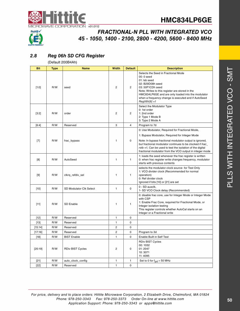
For price, delivery and to place orders: Hittite Microwave Corporation, 2 Elizabeth Drive, Chelmsford, MA 01824Phone: 978-250-3343 Fax: 978-250-3373 Order On-line at www.hittite.com
Application Support: Phone: 978-250-3343 or [email protected]
PLL
s w
ith
int
eg
rat
ed
VC
O -
sM
t
50
HMC834LP6GEv01.0112
Fractional-n Pll with integrated Vco45 - 1050, 1400 - 2100, 2800 - 4200, 5600 - 8400 Mhz
2.8 reg 06h Sd cFg register (default 200B4ah)
Bit Type Name Width Default Description
[1:0] r/w seed 2 2
selects the seed in Fractional Mode00: 0 seed01: lsb seed02: B29d08h seed03: 50F1Cdh seednote; writes to this register are stored in the hMC834LP6ge and are only loaded into the modulator when a frequency change is executed and if autoseed Reg06h[8] =1
[3:2] r/w order 2 2
select the Modulator type0: 1st order1: 2nd order2: type 1 Mode B3: type 2 Mode a
[6:4] r/w reserved 3 4 Program to 7d
[7] r/w frac_bypass 1 0
0: Use Modulator, required for Fractional Mode,
1: Bypass Modulator, required for integer Mode
note: in bypass fractional modulator output is ignored, but fractional modulator continues to be clocked if frac_rstb =1, Can be used to test the isolation of the digital fractional modulator from the VCO output in integer mode
[8] r/w autoseed 1 11: loads the seed whenever the frac register is written0: when frac register write changes frequency, modulator starts with previous contents
[9] r/w clkrq_refdiv_sel 1 1
selects the modulator clock source- for test Only1: VCO divider clock (recommended for normal operation)0: ref divider clockignored if bits [10] or [21] are set
[10] r/w sd Modulator Clk select 1 00 - sd auxclk, 1- sd VCO Clock delay (recommended)
[11] r/w sd enable 1 1
0: disable frac core, use for integer Mode or integer Modewith CsP1: enable Frac Core, required for Fractional Mode, or integer isolation testingthis register controls whether autoCal starts on an integer or a Fractional write
[12] r/w reserved 1 0
[13] r/w reserved 1 0
[15:14] r/w reserved 2 0
[17:16] r/w reserved 2 0 Program to 3d
[18] r/w Bist enable 1 0 enable Built in self test
[20:19] r/w rdiv Bist Cycles 2 0
rdiv Bist Cycles00: 103201: 204710: 307111: 4095
[21] r/w auto_clock_config 1 1 set to 0 for fpd > 50 Mhz
[22] r/w reserved 1 0
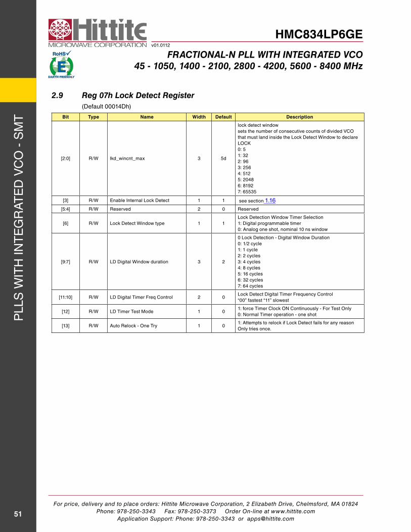
For price, delivery and to place orders: Hittite Microwave Corporation, 2 Elizabeth Drive, Chelmsford, MA 01824Phone: 978-250-3343 Fax: 978-250-3373 Order On-line at www.hittite.com
Application Support: Phone: 978-250-3343 or [email protected]
PLL
s w
ith
int
eg
rat
ed
VC
O -
sM
t
51
HMC834LP6GEv01.0112
Fractional-n Pll with integrated Vco45 - 1050, 1400 - 2100, 2800 - 4200, 5600 - 8400 Mhz
2.9 reg 07h lock detect register (default 00014dh)
Bit Type Name Width Default Description
[2:0] r/w lkd_wincnt_max 3 5d
lock detect window sets the number of consecutive counts of divided VCO that must land inside the Lock detect window to declare LOCK0: 51: 322: 963: 2564: 5125: 20486: 81927: 65535
[3] r/w enable internal Lock detect 1 1 see section 1.16[5:4] r/w reserved 2 0 reserved
[6] r/w Lock detect window type 1 1Lock detection window timer selection1: digital programmable timer0: analog one shot, nominal 10 ns window
[9:7] r/w Ld digital window duration 3 2
0 Lock detection - digital window duration0: 1/2 cycle1: 1 cycle2: 2 cycles3: 4 cycles4: 8 cycles5: 16 cycles6: 32 cycles7: 64 cycles
[11:10] r/w Ld digital timer Freq Control 2 0Lock detect digital timer Frequency Control“00” fastest “11” slowest
[12] r/w Ld timer test Mode 1 01: force timer Clock On Continuously - For test Only0: normal timer operation - one shot
[13] r/w auto relock - One try 1 01: attempts to relock if Lock detect fails for any reasonOnly tries once.
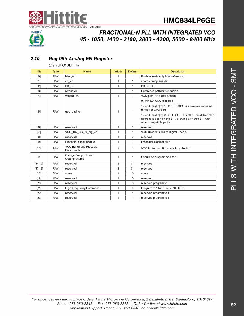
For price, delivery and to place orders: Hittite Microwave Corporation, 2 Elizabeth Drive, Chelmsford, MA 01824Phone: 978-250-3343 Fax: 978-250-3373 Order On-line at www.hittite.com
Application Support: Phone: 978-250-3343 or [email protected]
PLL
s w
ith
int
eg
rat
ed
VC
O -
sM
t
52
HMC834LP6GEv01.0112
Fractional-n Pll with integrated Vco45 - 1050, 1400 - 2100, 2800 - 4200, 5600 - 8400 Mhz
2.10 reg 08h analog en register (default C1BeFFh)
Bit type name width default description
[0] r/w bias_en 1 1 enables main chip bias reference
[1] r/w cp_en 1 1 charge pump enable
[2] r/w Pd_en 1 1 Pd enable
[3] r/w refbuf_en 1 reference path buffer enable
[4] r/w vcobuf_en 1 1 VCO path rF buffer enable
[5] r/w gpo_pad_en 1 1
0 - Pin Ld_sdO disabled
1 - and regFh[7]=1 , Pin Ld_sdO is always on required for use of gPO port
1 - and regFh[7]=0 sPi LdO_sPi is off if unmatched chip address is seen on the sPi, allowing a shared sPi with other compatible parts
[6] r/w reserved 1 1 reserved
[7] r/w VCO_div_Clk_to_dig_en 1 1 VCO divider Clock to digital enable
[8] r/w reserved 1 0 reserved
[9] r/w Prescaler Clock enable 1 1 Prescaler clock enable
[10] r/wVCO Buffer and PrescalerBias enable
1 1 VCO Buffer and Prescaler Bias enable
[11] r/wCharge Pump internalOpamp enable
1 1 should be programmed to 1
[14:12] r/w reserved 3 011 reserved
[17:15] r/w reserved 3 011 reserved
[18] r/w spare 1 0 spare
[19] r/w reserved 1 0 reserved
[20] r/w reserved 1 0 reserved program to 0
[21] r/w high Frequency reference 1 0 Program to 1 for XtaL > 200 Mhz
[22] r/w reserved 1 1 reserved program to 1
[23] r/w reserved 1 1 reserved program to 1
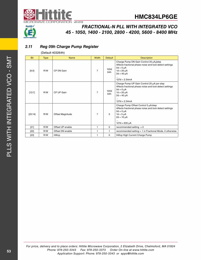
For price, delivery and to place orders: Hittite Microwave Corporation, 2 Elizabeth Drive, Chelmsford, MA 01824Phone: 978-250-3343 Fax: 978-250-3373 Order On-line at www.hittite.com
Application Support: Phone: 978-250-3343 or [email protected]
PLL
s w
ith
int
eg
rat
ed
VC
O -
sM
t
53
HMC834LP6GEv01.0112
Fractional-n Pll with integrated Vco45 - 1050, 1400 - 2100, 2800 - 4200, 5600 - 8400 Mhz
2.11 reg 09h charge Pump register (default 403264h)
Bit type name width default description
[6:0] r/w CP dn gain 7100d64h
Charge Pump dn gain Control 20 µa√stepaffects fractional phase noise and lock detect settings0d = 0 µa1d = 20 µa2d = 40 µa...127d = 2.54ma
[13:7] r/w CP UP gain 7100d64h
Charge Pump UP gain Control 20 µa per stepaffects fractional phase noise and lock detect settings0d = 0 µa1d = 20 µa2d = 40 µa...127d = 2.54ma
[20:14] r/w Offset Magnitude 7 0
Charge Pump Offset Control 5 µa/stepaffects fractional phase noise and lock detect settings0d = 0 µa1d = 5 µa2d = 10 µa...127d = 635 µa
[21] r/w Offset UP enable 1 0 recommended setting = 0
[22] r/w Offset dn enable 1 1 recommended setting = 1 in Fractional Mode, 0 otherwise
[23] r/w hiKcp 1 0 hiKcp high Current Charge Pump
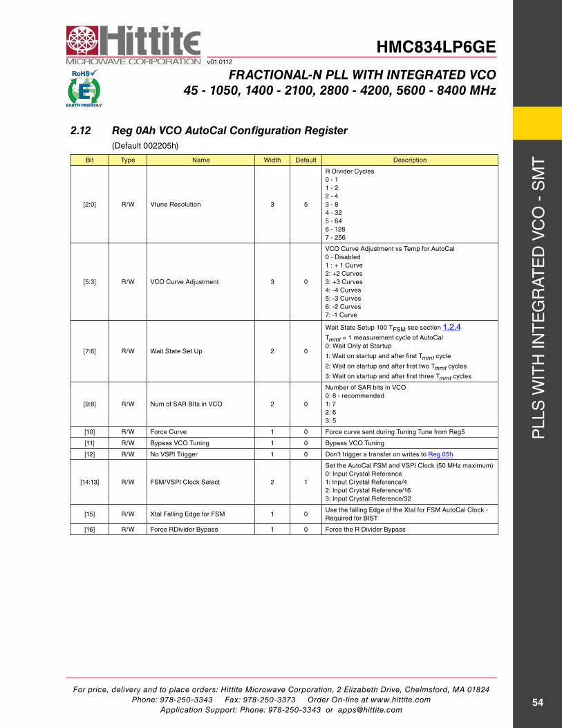
For price, delivery and to place orders: Hittite Microwave Corporation, 2 Elizabeth Drive, Chelmsford, MA 01824Phone: 978-250-3343 Fax: 978-250-3373 Order On-line at www.hittite.com
Application Support: Phone: 978-250-3343 or [email protected]
PLL
s w
ith
int
eg
rat
ed
VC
O -
sM
t
54
HMC834LP6GEv01.0112
Fractional-n Pll with integrated Vco45 - 1050, 1400 - 2100, 2800 - 4200, 5600 - 8400 Mhz
2.12 reg 0ah Vco autocal configuration register (default 002205h)
Bit type name width default description
[2:0] r/w Vtune resolution 3 5
r divider Cycles0 - 11 - 22 - 43 - 84 - 325 - 646 - 1287 - 256
[5:3] r/w VCO Curve adjustment 3 0
VCO Curve adjustment vs temp for autoCal0 - disabled1 : + 1 Curve2: +2 Curves3: +3 Curves4: -4 Curves5: -3 Curves6: -2 Curves7: -1 Curve
[7:6] r/w wait state set Up 2 0
wait state setup 100 tFsM see section 1.2.4
tmmt = 1 measurement cycle of autoCal 0: wait Only at startup
1: wait on startup and after first tmmt cycle
2: wait on startup and after first two tmmt cycles
3: wait on startup and after first three tmmt cycles
[9:8] r/w num of sar Bits in VCO 2 0
number of sar bits in VCO0: 8 - recommended1: 72: 63: 5
[10] r/w Force Curve 1 0 Force curve sent during tuning tune from reg5
[11] r/w Bypass VCO tuning 1 0 Bypass VCO tuning
[12] r/w no VsPi trigger 1 0 don’t trigger a transfer on writes to reg 05h
[14:13] r/w FsM/VsPi Clock select 2 1
set the autoCal FsM and VsPi Clock (50 Mhz maximum)0: input Crystal reference1: input Crystal reference/42: input Crystal reference/163: input Crystal reference/32
[15] r/w Xtal Falling edge for FsM 1 0Use the falling edge of the Xtal for FsM autoCal Clock - required for Bist
[16] r/w Force rdivider Bypass 1 0 Force the r divider Bypass
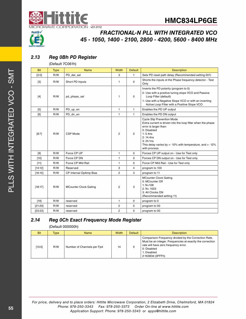
For price, delivery and to place orders: Hittite Microwave Corporation, 2 Elizabeth Drive, Chelmsford, MA 01824Phone: 978-250-3343 Fax: 978-250-3373 Order On-line at www.hittite.com
Application Support: Phone: 978-250-3343 or [email protected]
PLL
s w
ith
int
eg
rat
ed
VC
O -
sM
t
55
HMC834LP6GEv01.0112
Fractional-n Pll with integrated Vco45 - 1050, 1400 - 2100, 2800 - 4200, 5600 - 8400 Mhz
2.13 reg 0Bh Pd register (default 7C061h)
Bit type name width default description
[2:0] r/w Pd_del_sel 3 1 sets Pd reset path delay (recommended setting 001)
[3] r/w short Pd inputs 1 0shorts the inputs ot the Phase frequency detector - test Only
[4] r/w pd_phase_sel 1 0
inverts the Pd polarity (program to 0)
0- Use with a positive tuning slope VCO and Passive Loop Filter (default)
1- Use with a negative slope VCO or with an inverting active Loop Filter with a Positive slope VCO
[5] r/w Pd_up_en 1 1 enables the Pd UP output
[6] r/w Pd_dn_en 1 1 enables the Pd dn output
[8:7] r/w CsP Mode 2 0
Cycle slip Prevention Modeextra current is driven into the loop filter when the phase error is larger than:0: disabled1: 5.4ns2: 14.4ns3: 24.1nsthis delay varies by +- 10% with temperature, and +- 12% with process.
[9] r/w Force CP UP 1 0 Forces CP UP output on - Use for test only
[10] r/w Force CP dn 1 0 Forces CP dn output on - Use for test only
[11] r/w Force CP Mid rail 1 0 Force CP Mid rail - Use for test only
[14:12] r/w reserved 3 4 program to 100
[16:15] r/w CP internal Opamp Bias 2 3 program to 11
[18:17] r/w MCounter Clock gating 2 3
MCounter Clock gating0: MCounter Off1: n<1282: n< 10233: all Clocks On(recommended setting 11)
[19] r/w reserved 1 0 program to 0
[21:20] r/w reserved 2 0 program to 00
[23:22] r/w reserved 2 0 program to 00
2.14 reg 0ch exact Frequency Mode register (default 000000h)
Bit type name width default description
[13:0] r/w number of Channels per Fpd 14 0
Comparison Frequency divided by the Correction rate, Must be an integer. Frequencies at exactly the correction rate will have zero frequency error.0: disabled1: disabled2:16383d (3FFFh)
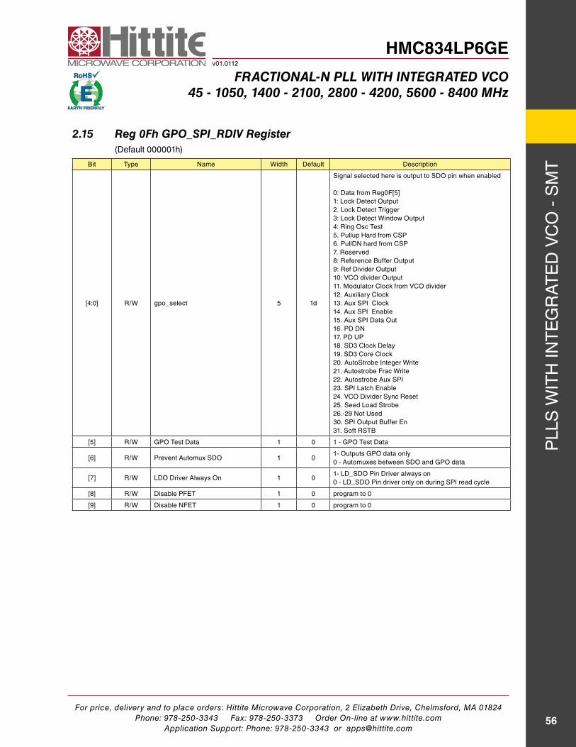
For price, delivery and to place orders: Hittite Microwave Corporation, 2 Elizabeth Drive, Chelmsford, MA 01824Phone: 978-250-3343 Fax: 978-250-3373 Order On-line at www.hittite.com
Application Support: Phone: 978-250-3343 or [email protected]
PLL
s w
ith
int
eg
rat
ed
VC
O -
sM
t
56
HMC834LP6GEv01.0112
Fractional-n Pll with integrated Vco45 - 1050, 1400 - 2100, 2800 - 4200, 5600 - 8400 Mhz
2.15 reg 0Fh gPo_SPi_rdiV register (default 000001h)
Bit type name width default description
[4:0] r/w gpo_select 5 1d
signal selected here is output to sdO pin when enabled
0: data from reg0F[5]1: Lock detect Output 2. Lock detect trigger3: Lock detect window Output4: ring Osc test5. Pullup hard from CsP6. Pulldn hard from CsP7. reserved8: reference Buffer Output9: ref divider Output10: VCO divider Output 11. Modulator Clock from VCO divider12. auxiliary Clock13. aux sPi Clock14. aux sPi enable15. aux sPi data Out16. Pd dn17. Pd UP18. sd3 Clock delay19. sd3 Core Clock20. autostrobe integer write21. autostrobe Frac write22. autostrobe aux sPi23. sPi Latch enable24. VCO divider sync reset25. seed Load strobe26.-29 not Used30. sPi Output Buffer en31. soft rstB
[5] r/w gPO test data 1 0 1 - gPO test data
[6] r/w Prevent automux sdO 1 01- Outputs gPO data only0 - automuxes between sdO and gPO data
[7] r/w LdO driver always On 1 01- Ld_sdO Pin driver always on0 - Ld_sdO Pin driver only on during sPi read cycle
[8] r/w disable PFet 1 0 program to 0
[9] r/w disable nFet 1 0 program to 0
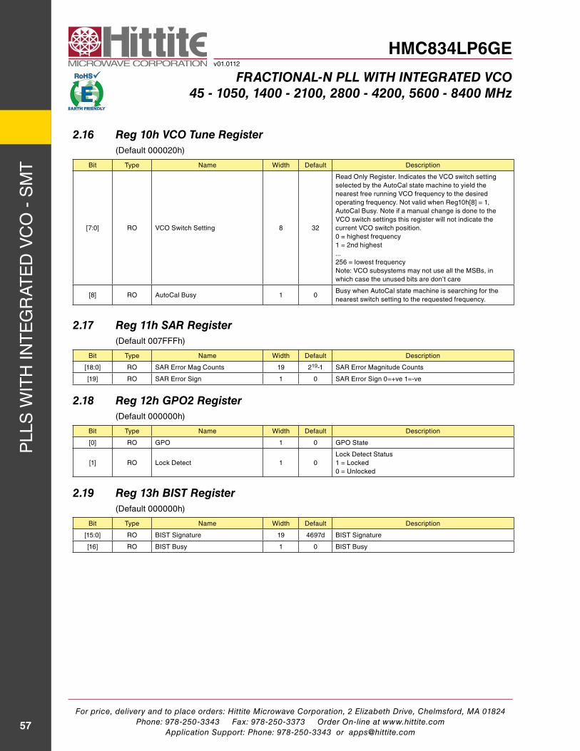
For price, delivery and to place orders: Hittite Microwave Corporation, 2 Elizabeth Drive, Chelmsford, MA 01824Phone: 978-250-3343 Fax: 978-250-3373 Order On-line at www.hittite.com
Application Support: Phone: 978-250-3343 or [email protected]
PLL
s w
ith
int
eg
rat
ed
VC
O -
sM
t
57
HMC834LP6GEv01.0112
Fractional-n Pll with integrated Vco45 - 1050, 1400 - 2100, 2800 - 4200, 5600 - 8400 Mhz
2.16 reg 10h Vco tune register (default 000020h)
Bit type name width default description
[7:0] rO VCO switch setting 8 32
read Only register. indicates the VCO switch setting selected by the autoCal state machine to yield the nearest free running VCO frequency to the desired operating frequency. not valid when reg10h[8] = 1, autoCal Busy. note if a manual change is done to the VCO switch settings this register will not indicate the current VCO switch position. 0 = highest frequency1 = 2nd highest...256 = lowest frequencynote: VCO subsystems may not use all the MsBs, in which case the unused bits are don’t care
[8] rO autoCal Busy 1 0Busy when autoCal state machine is searching for the nearest switch setting to the requested frequency.
2.17 reg 11h Sar register (default 007FFFh)
Bit type name width default description
[18:0] rO sar error Mag Counts 19 219-1 sar error Magnitude Counts
[19] rO sar error sign 1 0 sar error sign 0=+ve 1=-ve
2.18 reg 12h gPo2 register (default 000000h)
Bit type name width default description
[0] rO gPO 1 0 gPO state
[1] rO Lock detect 1 0Lock detect status1 = Locked0 = Unlocked
2.19 reg 13h BiSt register (default 000000h)
Bit type name width default description
[15:0] rO Bist signature 19 4697d Bist signature
[16] rO Bist Busy 1 0 Bist Busy
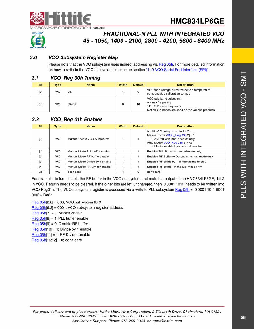
For price, delivery and to place orders: Hittite Microwave Corporation, 2 Elizabeth Drive, Chelmsford, MA 01824Phone: 978-250-3343 Fax: 978-250-3373 Order On-line at www.hittite.com
Application Support: Phone: 978-250-3343 or [email protected]
PLL
s w
ith
int
eg
rat
ed
VC
O -
sM
t
58
HMC834LP6GEv01.0112
Fractional-n Pll with integrated Vco45 - 1050, 1400 - 2100, 2800 - 4200, 5600 - 8400 Mhz
3.0 Vco Subsystem register MapPlease note that the VCO subsystem uses indirect addressing via reg 05h. For more detailed information on how to write to the VCO subsystem please see section “1.19 VCO serial Port interface (sPi)”.
3.1 Vco_reg 00h tuningBit Type Name Width Default Description
[0] wO Cal 1 0VCO tune voltage is redirected to a temperature compensated calibration voltage
[8:1] wO CaPs 8 16
VCO sub-band selection. 0 - max frequency1111 1111 - min frequency.not all sub-bands are used on the various products.
3.2 Vco_reg 01h enablesBit Type Name Width Default Description
[0] wO Master enable VCO subsystem 1 1
0 - all VCO subsystem blocks OffManual mode (VCO_reg 03h[2] = 1)
1- anded with local enables onlyauto Mode (VCO_reg 03h[2] = 0)
1- Master enable ignores local enables
[1] wO Manual Mode PLL buffer enable 1 1 enables PLL Buffer in manual mode only
[2] wO Manual Mode rF buffer enable 1 1 enables rF Buffer to Output in manual mode only
[3] wO Manual Mode divide by 1 enable 1 1 enables rF divide by 1 in manual mode only
[4] wO Manual Mode rF divider enable 1 1 enables rF divider in manual mode only
[8:5] wO don’t care 4 0 don’t care
For example, to turn disable the rF buffer in the VCO subsystem and mute the output of the hMC834LP6ge, bit 2 in VCO_reg01h needs to be cleared. if the other bits are left unchanged, then ‘0 0001 1011’ needs to be written into VCO reg01h. the VCO subsystem register is accessed via a write to PLL subsystem reg 05h = ‘0 0001 1011 0001 000’ = d88h
reg 05h[2:0] = 000; VCO subsystem id 0reg 05h[6:3] = 0001; VCO subsystem register addressreg 05h[7] = 1; Master enablereg 05h[8] = 1; PLL buffer enablereg 05h[9] = 0; disable rF bufferreg 05h[10] = 1; divide by 1 enablereg 05h[11] = 1; rF divider enablereg 05h[16:12] = 0; don’t care
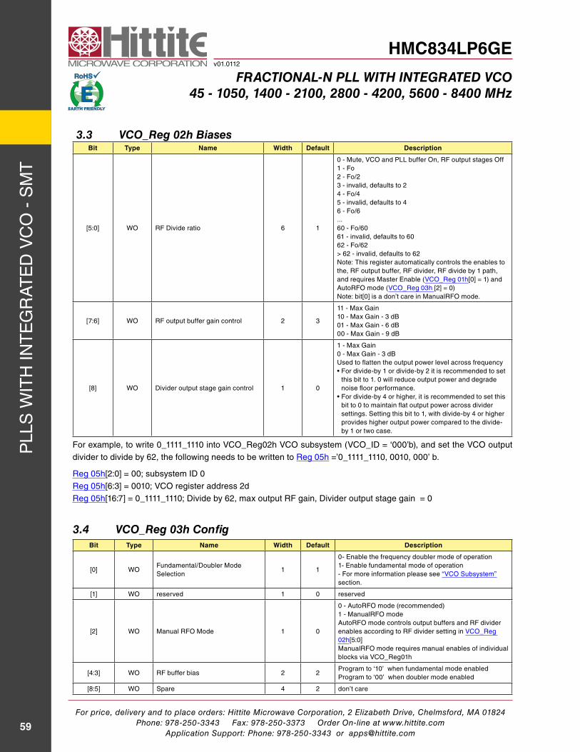
For price, delivery and to place orders: Hittite Microwave Corporation, 2 Elizabeth Drive, Chelmsford, MA 01824Phone: 978-250-3343 Fax: 978-250-3373 Order On-line at www.hittite.com
Application Support: Phone: 978-250-3343 or [email protected]
PLL
s w
ith
int
eg
rat
ed
VC
O -
sM
t
59
HMC834LP6GEv01.0112
Fractional-n Pll with integrated Vco45 - 1050, 1400 - 2100, 2800 - 4200, 5600 - 8400 Mhz
3.3 Vco_reg 02h BiasesBit Type Name Width Default Description
[5:0] wO rF divide ratio 6 1
0 - Mute, VCO and PLL buffer On, rF output stages Off1 - Fo2 - Fo/23 - invalid, defaults to 24 - Fo/45 - invalid, defaults to 46 - Fo/6...60 - Fo/6061 - invalid, defaults to 6062 - Fo/62> 62 - invalid, defaults to 62note: this register automatically controls the enables to the, rF output buffer, rF divider, rF divide by 1 path, and requires Master enable (VCO_reg 01h[0] = 1) and autorFO mode (VCO_reg 03h [2] = 0)note: bit[0] is a don’t care in ManualrFO mode.
[7:6] wO rF output buffer gain control 2 3
11 - Max gain10 - Max gain - 3 dB01 - Max gain - 6 dB00 - Max gain - 9 dB
[8] wO divider output stage gain control 1 0
1 - Max gain0 - Max gain - 3 dBUsed to flatten the output power level across frequency•For divide-by 1 or divide-by 2 it is recommended to set
this bit to 1. 0 will reduce output power and degrade noise floor performance.
•For divide-by 4 or higher, it is recommended to set this bit to 0 to maintain flat output power across divider settings. setting this bit to 1, with divide-by 4 or higher provides higher output power compared to the divide-by 1 or two case.
For example, to write 0_1111_1110 into VCO_reg02h VCO subsystem (VCO_id = ‘000’b), and set the VCO output divider to divide by 62, the following needs to be written to reg 05h =’0_1111_1110, 0010, 000’ b.
reg 05h[2:0] = 00; subsystem id 0reg 05h[6:3] = 0010; VCO register address 2dreg 05h[16:7] = 0_1111_1110; divide by 62, max output rF gain, divider output stage gain = 0
3.4 Vco_reg 03h configBit Type Name Width Default Description
[0] wOFundamental/doubler Mode selection
1 1
0- enable the frequency doubler mode of operation1- enable fundamental mode of operation- For more information please see “VCO subsystem” section.
[1] wO reserved 1 0 reserved
[2] wO Manual rFO Mode 1 0
0 - autorFO mode (recommended)1 - ManualrFO modeautorFO mode controls output buffers and rF divider enables according to rF divider setting in VCO_reg 02h[5:0]ManualrFO mode requires manual enables of individual blocks via VCO_reg01h
[4:3] wO rF buffer bias 2 2Program to ‘10’ when fundamental mode enabledProgram to ‘00’ when doubler mode enabled
[8:5] wO spare 4 2 don’t care
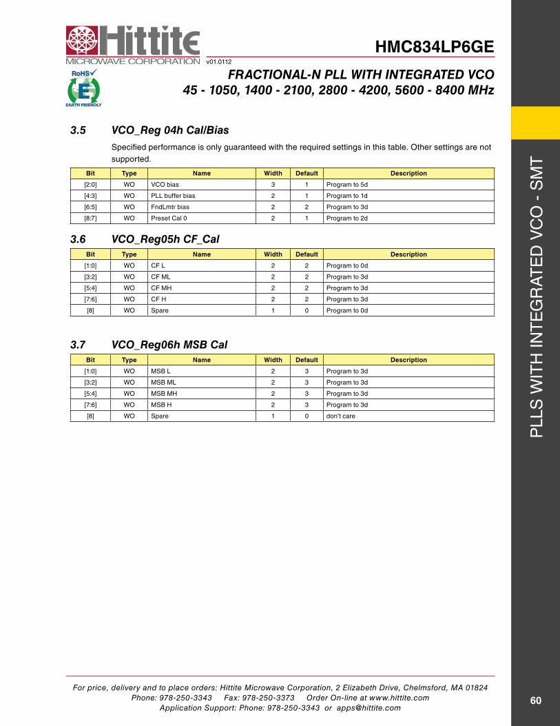
For price, delivery and to place orders: Hittite Microwave Corporation, 2 Elizabeth Drive, Chelmsford, MA 01824Phone: 978-250-3343 Fax: 978-250-3373 Order On-line at www.hittite.com
Application Support: Phone: 978-250-3343 or [email protected]
PLL
s w
ith
int
eg
rat
ed
VC
O -
sM
t
60
HMC834LP6GEv01.0112
Fractional-n Pll with integrated Vco45 - 1050, 1400 - 2100, 2800 - 4200, 5600 - 8400 Mhz
3.5 Vco_reg 04h cal/Biasspecified performance is only guaranteed with the required settings in this table. Other settings are not supported.
Bit Type Name Width Default Description
[2:0] wO VCO bias 3 1 Program to 5d
[4:3] wO PLL buffer bias 2 1 Program to 1d
[6:5] wO FndLmtr bias 2 2 Program to 3d
[8:7] wO Preset Cal 0 2 1 Program to 2d
3.6 Vco_reg05h cF_calBit Type Name Width Default Description
[1:0] wO CF L 2 2 Program to 0d
[3:2] wO CF ML 2 2 Program to 3d
[5:4] wO CF Mh 2 2 Program to 3d
[7:6] wO CF h 2 2 Program to 3d
[8] wO spare 1 0 Program to 0d
3.7 Vco_reg06h MSB calBit Type Name Width Default Description
[1:0] wO MsB L 2 3 Program to 3d
[3:2] wO MsB ML 2 3 Program to 3d
[5:4] wO MsB Mh 2 3 Program to 3d
[7:6] wO MsB h 2 3 Program to 3d
[8] wO spare 1 0 don’t care
For price, delivery and to place orders: Hittite Microwave Corporation, 2 Elizabeth Drive, Chelmsford, MA 01824Phone: 978-250-3343 Fax: 978-250-3373 Order On-line at www.hittite.com
Application Support: Phone: 978-250-3343 or [email protected]
PLL
s w
ith
int
eg
rat
ed
VC
O -
sM
t
61
HMC834LP6GEv01.0112
Fractional-n Pll with integrated Vco45 - 1050, 1400 - 2100, 2800 - 4200, 5600 - 8400 Mhz
noteS: