Embed Size (px)
Citation preview
Analog Devices Welcomes Hittite Microwave Corporation
NO CONTENT ON THE ATTACHED DOCUMENT HAS CHANGED
www.analog.com www.hittite.com

THIS PAGE INTENTIONALLY LEFT BLANK
Am
pli
fie
rs
- l
ine
Ar
& p
ow
er
- C
hip
3
3 - 1For price, delivery and to place orders: Hittite Microwave Corporation, 2 Elizabeth Drive, Chelmsford, MA 01824
Phone: 978-250-3343 Fax: 978-250-3373 Order On-line at www.hittite.comApplication Support: Phone: 978-250-3343 or [email protected]
HMC797GaAs PHEMT MMIC
1 WATT POWER AMPLIFIER, DC - 22 GHz
v02.1011
General Description
Features
Functional Diagram
The hmC797 is a GaAs mmiC phemT Distributed power Amplifier die which operates between DC and 22 Ghz. The amplifier provides 14.5 dB of gain, 40 dBm output ip3 and +28 dBm of output power at 1 dB gain compression while requiring 400mA from a +10V supply. This versatile pA exhibits a posi-tive gain slope from 3 to 21 Ghz making it ideal for ew, eCm, radar and test equipment applications. The hmC797 amplifier i/os are internally matched to 50 ohms facilitating integration into mutli-Chip-modules (mCms). All data is taken with the chip connected via two 0.025mm (1 mil) wire bonds of mini-mal length 0.31 mm (12 mils).
high p1dB output power: +28 dBm
high psat output power: +31 dBm
high Gain: 14.5 dB
high output ip3: +40 dBm
supply Voltage: +10 V @ 400 mA
50 ohm matched input/output
Die size: 2.89 x 1.55 x 0.1 mm
Typical Applications
The hmC797 is ideal for:
• Test instrumentation
• microwave radio & VsAT
• military & space
• Telecom infrastructure
• fiber optics
Electrical Specifications, TA = +25° C, Vdd = +10V, Vgg2 = +3.5V, Idd = 400 mA*
parameter min. Typ. max. min. Typ. max. min. Typ. max. Units
frequency range DC - 10 10 - 18 18 - 22 Ghz
Gain 13.5 14.5 15.5 dB
Gain flatness ±0.5 ±0.7 ±0.4 dB
Gain Variation over Temperature 0.009 0.01 0.012 dB/ °C
input return loss 16 17 18 dB
output return loss 16 18 17 dB
output power for 1 dB Compression (p1dB) 27 28.5 27 28.5 26.5 28 dBm
saturated output power (psat) 31 31 31 dBm
output Third order intercept (ip3) 41 40 39 dBm
noise figure 3.5 3 3.5 dB
supply Current(idd) (Vdd= 10V, Vgg1= -0.8V Typ.)
400 400 400 mA
* Adjust Vgg1 between -2 to 0V to achieve Idd = 400 mA typical.
Am
pli
fie
rs
- l
ine
Ar
& p
ow
er
- C
hip
3
3 - 2For price, delivery and to place orders: Hittite Microwave Corporation, 2 Elizabeth Drive, Chelmsford, MA 01824
Phone: 978-250-3343 Fax: 978-250-3373 Order On-line at www.hittite.comApplication Support: Phone: 978-250-3343 or [email protected]
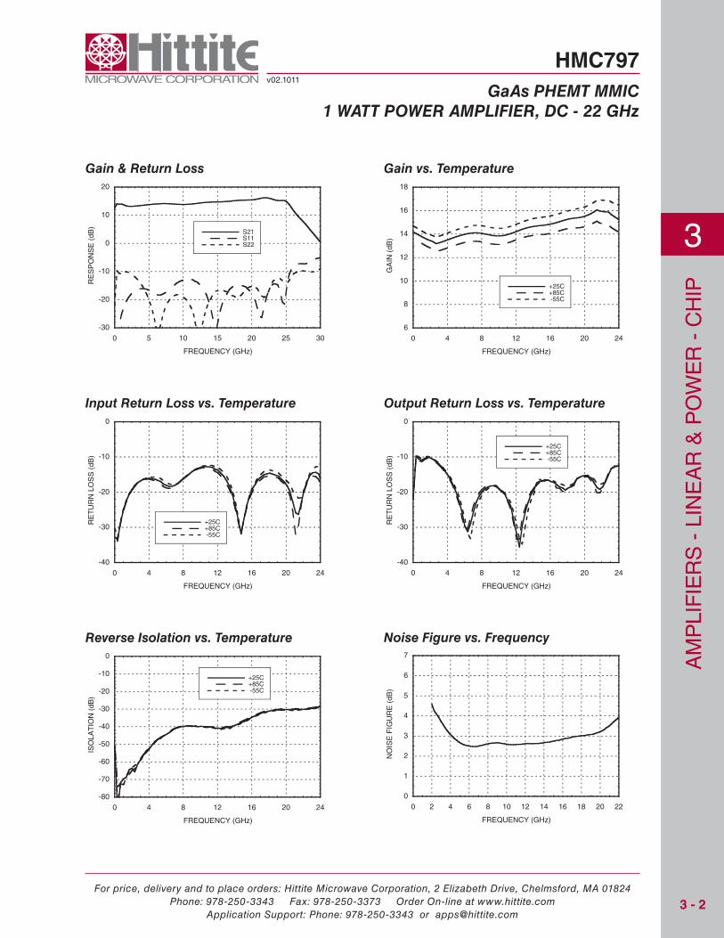
Output Return Loss vs. Temperature
Gain & Return Loss Gain vs. Temperature
Reverse Isolation vs. Temperature
Input Return Loss vs. Temperature
Noise Figure vs. Frequency
HMC797v02.1011
GaAs PHEMT MMIC 1 WATT POWER AMPLIFIER, DC - 22 GHz
-30
-20
-10
0
10
20
0 5 10 15 20 25 30
S21S11S22
RE
SP
ON
SE
(dB
)
FREQUENCY (GHz)
-40
-30
-20
-10
0
0 4 8 12 16 20 24
+25C+85C -55C
RE
TU
RN
LO
SS
(dB
)
FREQUENCY (GHz)
-80
-70
-60
-50
-40
-30
-20
-10
0
0 4 8 12 16 20 24
+25C+85C -55C
ISO
LAT
ION
(dB
)
FREQUENCY (GHz)
0
1
2
3
4
5
6
7
0 2 4 6 8 10 12 14 16 18 20 22
NO
ISE
FIG
UR
E (
dB)
FREQUENCY (GHz)
-40
-30
-20
-10
0
0 4 8 12 16 20 24
+25C+85C -55C
RE
TU
RN
LO
SS
(dB
)
FREQUENCY (GHz)
6
8
10
12
14
16
18
0 4 8 12 16 20 24
+25C+85C -55C
GA
IN (
dB)
FREQUENCY (GHz)
Am
pli
fie
rs
- l
ine
Ar
& p
ow
er
- C
hip
3
3 - 3For price, delivery and to place orders: Hittite Microwave Corporation, 2 Elizabeth Drive, Chelmsford, MA 01824
Phone: 978-250-3343 Fax: 978-250-3373 Order On-line at www.hittite.comApplication Support: Phone: 978-250-3343 or [email protected]
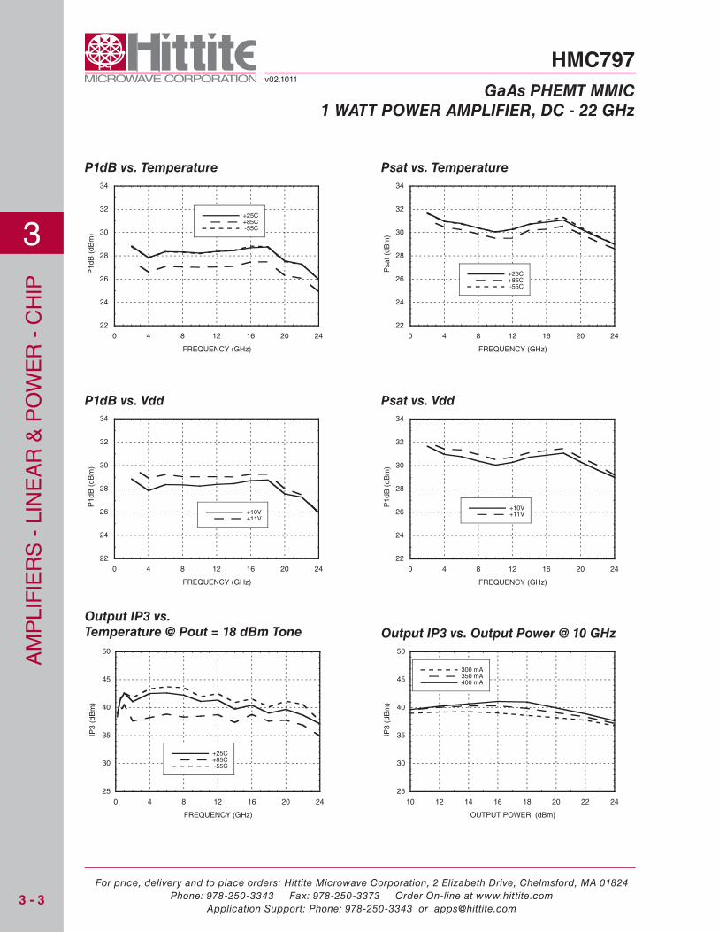
Output IP3 vs. Output Power @ 10 GHz
Psat vs. Vdd
P1dB vs. Temperature Psat vs. Temperature
Output IP3 vs. Temperature @ Pout = 18 dBm Tone
P1dB vs. Vdd
HMC797v02.1011
GaAs PHEMT MMIC 1 WATT POWER AMPLIFIER, DC - 22 GHz
22
24
26
28
30
32
34
0 4 8 12 16 20 24
+25C+85C -55C
P1d
B (
dBm
)
FREQUENCY (GHz)
22
24
26
28
30
32
34
0 4 8 12 16 20 24
+25C+85C -55C
Psa
t (dB
m)
FREQUENCY (GHz)
25
30
35
40
45
50
10 12 14 16 18 20 22 24
300 mA350 mA400 mA
IP3
(dB
m)
OUTPUT POWER (dBm)
25
30
35
40
45
50
0 4 8 12 16 20 24
+25C+85C -55C
IP3
(dB
m)
FREQUENCY (GHz)
22
24
26
28
30
32
34
0 4 8 12 16 20 24
+10V+11V
P1d
B (
dBm
)
FREQUENCY (GHz)
22
24
26
28
30
32
34
0 4 8 12 16 20 24
+10V+11V
P1d
B (
dBm
)
FREQUENCY (GHz)
Am
pli
fie
rs
- l
ine
Ar
& p
ow
er
- C
hip
3
3 - 4For price, delivery and to place orders: Hittite Microwave Corporation, 2 Elizabeth Drive, Chelmsford, MA 01824
Phone: 978-250-3343 Fax: 978-250-3373 Order On-line at www.hittite.comApplication Support: Phone: 978-250-3343 or [email protected]
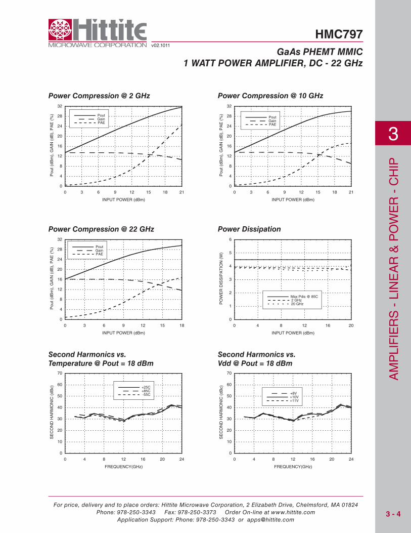
Power Compression @ 22 GHz
Second Harmonics vs. Temperature @ Pout = 18 dBm
Power Dissipation
Second Harmonics vs. Vdd @ Pout = 18 dBm
Power Compression @ 2 GHz Power Compression @ 10 GHz
HMC797v02.1011
GaAs PHEMT MMIC 1 WATT POWER AMPLIFIER, DC - 22 GHz
0
4
8
12
16
20
24
28
32
0 3 6 9 12 15 18 21
PoutGainPAE
Pou
t (dB
m),
GA
IN (
dB),
PA
E (
%)
INPUT POWER (dBm)
0
4
8
12
16
20
24
28
32
0 3 6 9 12 15 18 21
PoutGainPAE
Pou
t (dB
m),
GA
IN (
dB),
PA
E (
%)
INPUT POWER (dBm)
0
4
8
12
16
20
24
28
32
0 3 6 9 12 15 18
PoutGainPAE
Pou
t (dB
m),
GA
IN (
dB),
PA
E (
%)
INPUT POWER (dBm)
0
10
20
30
40
50
60
70
0 4 8 12 16 20 24
+25C+85C -55C
SE
CO
ND
HA
RM
ON
IC (
dBc)
FREQUENCY(GHz)
0
1
2
3
4
5
6
0 4 8 12 16 20
Max Pdis @ 85C2 GHz20 GHzP
OW
ER
DIS
SIP
AT
ION
(W
)
INPUT POWER (dBm)
0
10
20
30
40
50
60
70
0 4 8 12 16 20 24
+8V+10V+11V
SE
CO
ND
HA
RM
ON
IC (
dBc)
FREQUENCY(GHz)
Am
pli
fie
rs
- l
ine
Ar
& p
ow
er
- C
hip
3
3 - 5For price, delivery and to place orders: Hittite Microwave Corporation, 2 Elizabeth Drive, Chelmsford, MA 01824
Phone: 978-250-3343 Fax: 978-250-3373 Order On-line at www.hittite.comApplication Support: Phone: 978-250-3343 or [email protected]
HMC797v02.1011
GaAs PHEMT MMIC 1 WATT POWER AMPLIFIER, DC - 22 GHz
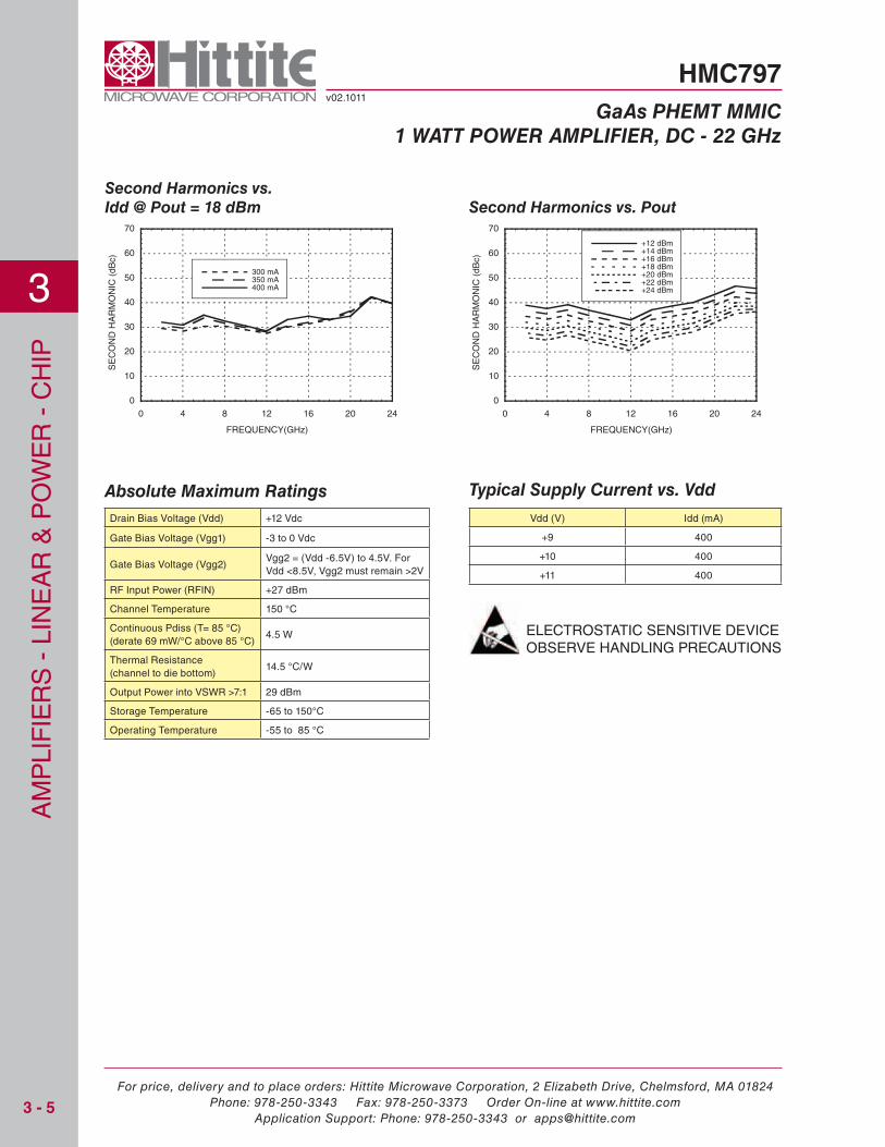
Absolute Maximum RatingsDrain Bias Voltage (Vdd) +12 Vdc
Gate Bias Voltage (Vgg1) -3 to 0 Vdc
Gate Bias Voltage (Vgg2)Vgg2 = (Vdd -6.5V) to 4.5V. for Vdd <8.5V, Vgg2 must remain >2V
rf input power (rfin) +27 dBm
Channel Temperature 150 °C
Continuous pdiss (T= 85 °C)(derate 69 mw/°C above 85 °C)
4.5 w
Thermal resistance (channel to die bottom)
14.5 °C/w
output power into Vswr >7:1 29 dBm
storage Temperature -65 to 150°C
operating Temperature -55 to 85 °C
Vdd (V) idd (mA)
+9 400
+10 400
+11 400
Typical Supply Current vs. Vdd
eleCTrosTATiC sensiTiVe DeViCeoBserVe hAnDlinG preCAUTions
Second Harmonics vs. Idd @ Pout = 18 dBm Second Harmonics vs. Pout
0
10
20
30
40
50
60
70
0 4 8 12 16 20 24
300 mA350 mA400 mA
SE
CO
ND
HA
RM
ON
IC (
dBc)
FREQUENCY(GHz)
0
10
20
30
40
50
60
70
0 4 8 12 16 20 24
+12 dBm+14 dBm+16 dBm+18 dBm+20 dBm+22 dBm+24 dBm
SE
CO
ND
HA
RM
ON
IC (
dBc)
FREQUENCY(GHz)
Am
pli
fie
rs
- l
ine
Ar
& p
ow
er
- C
hip
3
3 - 6For price, delivery and to place orders: Hittite Microwave Corporation, 2 Elizabeth Drive, Chelmsford, MA 01824
Phone: 978-250-3343 Fax: 978-250-3373 Order On-line at www.hittite.comApplication Support: Phone: 978-250-3343 or [email protected]
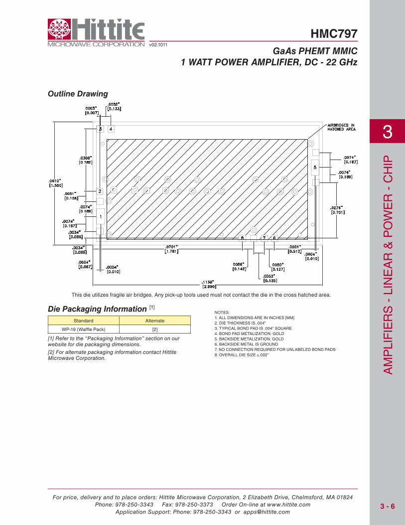
Outline Drawing
noTes:1. All Dimensions Are in inChes [mm]2. Die ThiCKness is .004”3. TYpiCAl BonD pAD is .004” sQUAre4. BonD pAD meTAliZATion: GolD5. BACKsiDe meTAliZATion: GolD6. BACKsiDe meTAl is GroUnD7. no ConneCTion reQUireD for UnlABeleD BonD pADs8. oVerAll Die siZe ±.002”
Die Packaging Information [1]
standard Alternate
wp-19 (waffle pack) [2]
[1] Refer to the “Packaging Information” section on our website for die packaging dimensions.
[2] For alternate packaging information contact Hittite Microwave Corporation.
HMC797v02.1011
GaAs PHEMT MMIC 1 WATT POWER AMPLIFIER, DC - 22 GHz
This die utilizes fragile air bridges. Any pick-up tools used must not contact the die in the cross hatched area.
Am
pli
fie
rs
- l
ine
Ar
& p
ow
er
- C
hip
3
3 - 7For price, delivery and to place orders: Hittite Microwave Corporation, 2 Elizabeth Drive, Chelmsford, MA 01824
Phone: 978-250-3343 Fax: 978-250-3373 Order On-line at www.hittite.comApplication Support: Phone: 978-250-3343 or [email protected]
HMC797v02.1011
GaAs PHEMT MMIC 1 WATT POWER AMPLIFIER, DC - 22 GHz
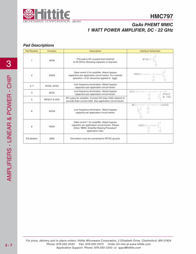
pad number function Description interface schematic
1 rfinThis pad is DC coupled and matched
to 50 ohms. Blocking capacitor is required.
2 VGG2Gate control 2 for amplifier. Attach bypass
capacitors per application circuit herein. for nominal operation +3.5V should be applied to Vgg2.
4, 7 ACG2, ACG4low frequency termination. Attach bypass capacitors per application circuit herein.
3 ACG1low frequency termination. Attach bypass capacitors per application circuit herein.
5 rfoUT & VDDrf output for amplifier. Connect DC bias (Vdd) network to provide drain current (idd). see application circuit herein.
6 ACG3low frequency termination. Attach bypass
capacitor per application circuit herein.
8 VGG1
Gate control 1 for amplifier. Attach bypass capacitor per application circuit herein. please
follow “mmiC Amplifier Biasing procedure” application note.
Die Bottom GnD Die bottom must be connected to rf/DC ground.
Pad Descriptions
Am
pli
fie
rs
- l
ine
Ar
& p
ow
er
- C
hip
3
3 - 8For price, delivery and to place orders: Hittite Microwave Corporation, 2 Elizabeth Drive, Chelmsford, MA 01824
Phone: 978-250-3343 Fax: 978-250-3373 Order On-line at www.hittite.comApplication Support: Phone: 978-250-3343 or [email protected]
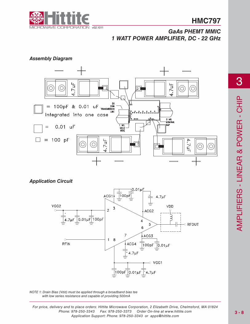
Application Circuit
NOTE 1: Drain Bias (Vdd) must be applied through a broadband bias tee with low series resistance and capable of providing 500mA
Assembly Diagram
HMC797v02.1011
GaAs PHEMT MMIC 1 WATT POWER AMPLIFIER, DC - 22 GHz
Am
pli
fie
rs
- l
ine
Ar
& p
ow
er
- C
hip
3
3 - 9For price, delivery and to place orders: Hittite Microwave Corporation, 2 Elizabeth Drive, Chelmsford, MA 01824
Phone: 978-250-3343 Fax: 978-250-3373 Order On-line at www.hittite.comApplication Support: Phone: 978-250-3343 or [email protected]
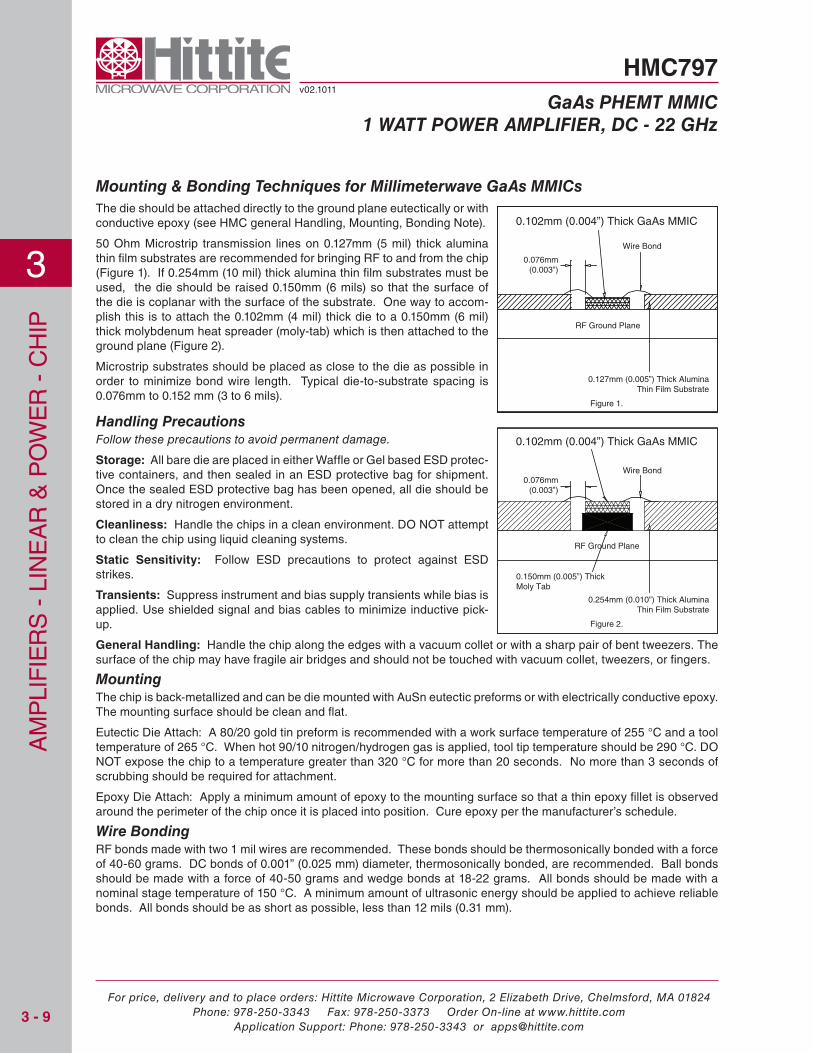
Mounting & Bonding Techniques for Millimeterwave GaAs MMICsThe die should be attached directly to the ground plane eutectically or with conductive epoxy (see hmC general handling, mounting, Bonding note).
50 ohm microstrip transmission lines on 0.127mm (5 mil) thick alumina thin film substrates are recommended for bringing rf to and from the chip (figure 1). if 0.254mm (10 mil) thick alumina thin film substrates must be used, the die should be raised 0.150mm (6 mils) so that the surface of the die is coplanar with the surface of the substrate. one way to accom-plish this is to attach the 0.102mm (4 mil) thick die to a 0.150mm (6 mil) thick molybdenum heat spreader (moly-tab) which is then attached to the ground plane (figure 2).
microstrip substrates should be placed as close to the die as possible in order to minimize bond wire length. Typical die-to-substrate spacing is 0.076mm to 0.152 mm (3 to 6 mils).
Handling PrecautionsFollow these precautions to avoid permanent damage.
Storage: All bare die are placed in either waffle or Gel based esD protec-tive containers, and then sealed in an esD protective bag for shipment. once the sealed esD protective bag has been opened, all die should be stored in a dry nitrogen environment.
Cleanliness: handle the chips in a clean environment. Do noT attempt to clean the chip using liquid cleaning systems.
Static Sensitivity: follow esD precautions to protect against esD strikes.
Transients: suppress instrument and bias supply transients while bias is applied. Use shielded signal and bias cables to minimize inductive pick-up.
General Handling: handle the chip along the edges with a vacuum collet or with a sharp pair of bent tweezers. The surface of the chip may have fragile air bridges and should not be touched with vacuum collet, tweezers, or fingers.
MountingThe chip is back-metallized and can be die mounted with Ausn eutectic preforms or with electrically conductive epoxy. The mounting surface should be clean and flat.
eutectic Die Attach: A 80/20 gold tin preform is recommended with a work surface temperature of 255 °C and a tool temperature of 265 °C. when hot 90/10 nitrogen/hydrogen gas is applied, tool tip temperature should be 290 °C. Do noT expose the chip to a temperature greater than 320 °C for more than 20 seconds. no more than 3 seconds of scrubbing should be required for attachment.
epoxy Die Attach: Apply a minimum amount of epoxy to the mounting surface so that a thin epoxy fillet is observed around the perimeter of the chip once it is placed into position. Cure epoxy per the manufacturer’s schedule.
Wire Bondingrf bonds made with two 1 mil wires are recommended. These bonds should be thermosonically bonded with a force of 40-60 grams. DC bonds of 0.001” (0.025 mm) diameter, thermosonically bonded, are recommended. Ball bonds should be made with a force of 40-50 grams and wedge bonds at 18-22 grams. All bonds should be made with a nominal stage temperature of 150 °C. A minimum amount of ultrasonic energy should be applied to achieve reliable bonds. All bonds should be as short as possible, less than 12 mils (0.31 mm).
0.102mm (0.004”) Thick GaAs MMIC
Wire Bond
RF Ground Plane
0.127mm (0.005”) Thick AluminaThin Film Substrate
0.076mm(0.003”)
Figure 1.
0.102mm (0.004”) Thick GaAs MMIC
Wire Bond
RF Ground Plane
0.254mm (0.010”) Thick AluminaThin Film Substrate
0.076mm(0.003”)
Figure 2.
0.150mm (0.005”) ThickMoly Tab
HMC797v02.1011
GaAs PHEMT MMIC 1 WATT POWER AMPLIFIER, DC - 22 GHz
Am
pli
fie
rs
- l
ine
Ar
& p
ow
er
- C
hip
3
3 - 10For price, delivery and to place orders: Hittite Microwave Corporation, 2 Elizabeth Drive, Chelmsford, MA 01824
Phone: 978-250-3343 Fax: 978-250-3373 Order On-line at www.hittite.comApplication Support: Phone: 978-250-3343 or [email protected]
Notes:
HMC797v02.1011
GaAs PHEMT MMIC 1 WATT POWER AMPLIFIER, DC - 22 GHz