Embed Size (px)
Citation preview
MO
DU
LAT
OR
S -
BI-
PH
AS
E -
CH
IP
5
5 - 2
For price, delivery, and to place orders, please contact Hittite Microwave Corporation:20 Alpha Road, Chelmsford, MA 01824 Phone: 978-250-3343 Fax: 978-250-3373
Order On-line at www.hittite.com
HMC135
GaAs MMIC BI-PHASE
MODULATOR, 1.8 - 5.2 GHz
v04.0909
General Description
Features
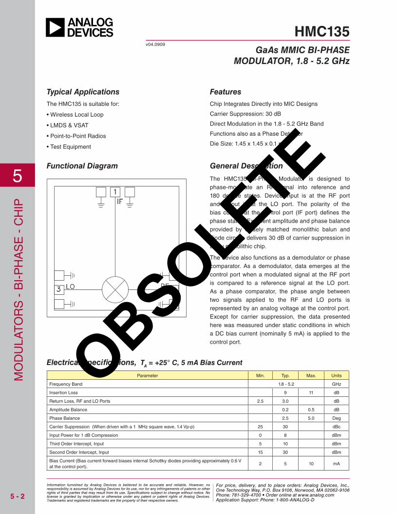
Functional Diagram
Chip Integrates Directly into MIC Designs
Carrier Suppression: 30 dB
Direct Modulation in the 1.8 - 5.2 GHz Band
Functions also as a Phase Detector
Die Size: 1.45 x 1.45 x 0.1 mm
Electrical Specifi cations, TA = +25° C, 5 mA Bias Current
Typical Applications
The HMC135 is suitable for:
• Wireless Local Loop
• LMDS & VSAT
• Point-to-Point Radios
• Test Equipment
The HMC135 Bi-Phase Modulator is designed to phase-modulate an RF signal into reference and 180 degree states. Device input is at the RF portand output is at the LO port. The polarity of the bias current at the control port (IF port) defi nes the phase states. Excellent amplitude and phase balance provided by closely matched monolithic balun and diode circuits delivers 30 dB of carrier suppression in a tiny monolithic chip.
The device also functions as a demodulator or phase comparator. As a demodulator, data emerges at the control port when a modulated signal at the RF port is compared to a reference signal at the LO port. As a phase comparator, the phase angle between two signals applied to the RF and LO ports is represented by an analog voltage at the control port. Except for carrier suppression, the data presented here was measured under static conditions in which a DC bias current (nominally 5 mA) is applied to the control port.
Parameter Min. Typ. Max. Units
Frequency Band 1.8 - 5.2 GHz
Insertion Loss 9 11 dB
Return Loss, RF and LO Ports 2.5 3.0 dB
Amplitude Balance 0.2 0.5 dB
Phase Balance 2.5 5.0 Deg
Carrier Suppression (When driven with a 1 MHz square wave, 1.4 Vp-p) 25 30 dBc
Input Power for 1 dB Compression 0 8 dBm
Third Order Intercept, Input 5 10 dBm
Second Order Intercept, Input 15 30 dBm
Bias Current (Bias current forward biases internal Schottky diodes providing approximately 0.6 V at the control port).
2 5 10 mA
OBSOLETE
Information furnished by Analog Devices is believed to be accurate and reliable. However, no responsibility is assumed by Analog Devices for its use, nor for any infringements of patents or other rights of third parties that may result from its use. Specifications subject to change without notice. No license is granted by implication or otherwise under any patent or patent rights of Analog Devices. Trademarks and registered trademarks are the property of their respective owners.
For price, delivery, and to place orders: Analog Devices, Inc., One Technology Way, P.O. Box 9106, Norwood, MA 02062-9106 Phone: 781-329-4700 • Order online at www.analog.com Application Support: Phone: 1-800-ANALOG-D
MO
DU
LAT
OR
S -
BI-
PH
AS
E -
CH
IP
5
5 - 3
For price, delivery, and to place orders, please contact Hittite Microwave Corporation:20 Alpha Road, Chelmsford, MA 01824 Phone: 978-250-3343 Fax: 978-250-3373
Order On-line at www.hittite.com
FREQUENCY (GHz)
654321
INS
ER
TIO
N L
OS
S (
dB)
0
-5
-10
-15
-20 -2
-1
0
1
2
AM
PLI
TU
DE
BA
LAN
CE
(dB
)
1 2 3 4 5 6
FREQUENCY (GHz)
-8
-10
-6
-4
-2
0
2
4
6
8
10
PH
AS
E B
ALA
NC
E (
Deg
)
1 2 3 4 5 6
FREQUENCY (GHz)
-20
-15
-10
-5
0
RE
TU
RN
LO
SS
(dB
)
0 1 2 3 4 5 6 7 8
FREQUENCY (GHz)
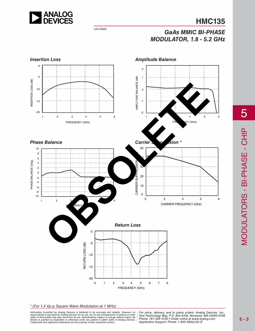
Return Loss
Insertion Loss Amplitude Balance
Phase Balance Carrier Suppression *
* (For 1.4 Vp-p Square Wave Modulation at 1 MHz)
0
10
20
30
40
50
CA
RR
IER
SU
PP
RE
SS
ION
(dB
c)
2 3 4 5 6
CARRIER FREQUENCY (GHz)
HMC135v04.0909
GaAs MMIC BI-PHASE
MODULATOR, 1.8 - 5.2 GHz
OBSOLETE
Information furnished by Analog Devices is believed to be accurate and reliable. However, no responsibility is assumed by Analog Devices for its use, nor for any infringements of patents or other rights of third parties that may result from its use. Specifications subject to change without notice. No license is granted by implication or otherwise under any patent or patent rights of Analog Devices. Trademarks and registered trademarks are the property of their respective owners.
For price, delivery, and to place orders: Analog Devices, Inc., One Technology Way, P.O. Box 9106, Norwood, MA 02062-9106 Phone: 781-329-4700 • Order online at www.analog.com Application Support: Phone: 1-800-ANALOG-D
MO
DU
LAT
OR
S -
BI-
PH
AS
E -
CH
IP
5
5 - 4
For price, delivery, and to place orders, please contact Hittite Microwave Corporation:20 Alpha Road, Chelmsford, MA 01824 Phone: 978-250-3343 Fax: 978-250-3373
Order On-line at www.hittite.com
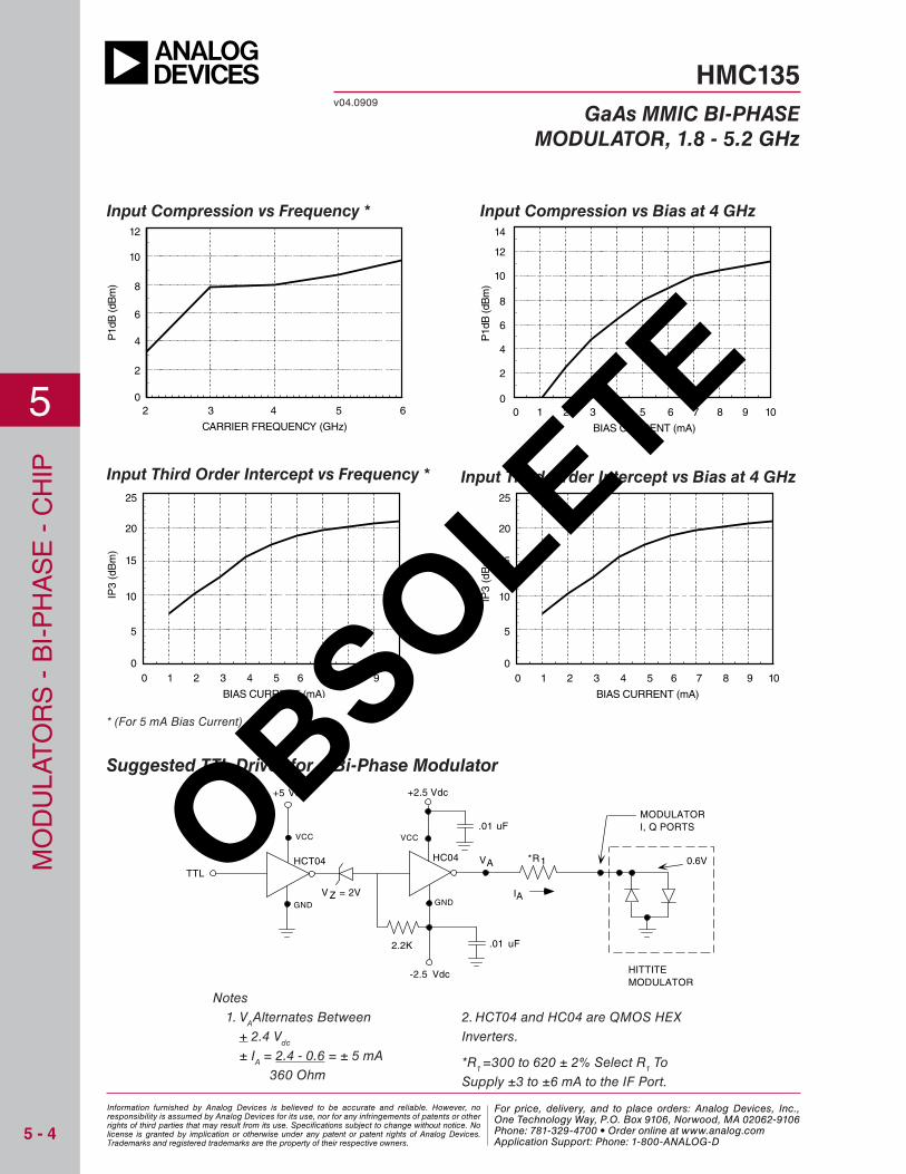
Input Compression vs Frequency * Input Compression vs Bias at 4 GHz
Input Third Order Intercept vs Frequency * Input Third Order Intercept vs Bias at 4 GHz
Suggested TTL Driver for a Bi-Phase Modulator
Notes 1. VAAlternates Between + 2.4 Vdc
± IA = 2.4 - 0.6 = ± 5 mA 360 Ohm
2. HCT04 and HC04 are QMOS HEX Inverters.
*R1 =300 to 620 ± 2% Select R1 To Supply ±3 to ±6 mA to the IF Port.
* (For 5 mA Bias Current)
0
2
4
6
8
10
12
P1d
B (d
Bm
)
2 3 4 5 6
CARRIER FREQUENCY (GHz)
0
2
4
6
8
10
12
14
P1d
B (d
Bm
)
BIAS CURRENT (mA)
0 1 2 3 4 5 6 7 8 9 10
0
5
10
15
20
25
IP3
(dB
m)
0 1 2 3 4 5 6 7 8 9 10
BIAS CURRENT (mA)
0
5
10
15
20
25IP
3 (d
Bm
)
0 1 2 3 4 5 6 7 8 9 10
BIAS CURRENT (mA)
2.2K
TTL
VCC
GNDGND
VCC
HCT04 HC04
.01 uF
.01 uF
-2.5 Vdc
+2.5 Vdc+5 Vdc
*R1
MODULATORI, Q PORTS
HITTITEMODULATOR
VA
IAV Z = 2V
0.6V
HMC135v04.0909
GaAs MMIC BI-PHASE
MODULATOR, 1.8 - 5.2 GHz
OBSOLETE
Information furnished by Analog Devices is believed to be accurate and reliable. However, no responsibility is assumed by Analog Devices for its use, nor for any infringements of patents or other rights of third parties that may result from its use. Specifications subject to change without notice. No license is granted by implication or otherwise under any patent or patent rights of Analog Devices. Trademarks and registered trademarks are the property of their respective owners.
For price, delivery, and to place orders: Analog Devices, Inc., One Technology Way, P.O. Box 9106, Norwood, MA 02062-9106 Phone: 781-329-4700 • Order online at www.analog.com Application Support: Phone: 1-800-ANALOG-D
MO
DU
LAT
OR
S -
BI-
PH
AS
E -
CH
IP
5
5 - 5
For price, delivery, and to place orders, please contact Hittite Microwave Corporation:20 Alpha Road, Chelmsford, MA 01824 Phone: 978-250-3343 Fax: 978-250-3373
Order On-line at www.hittite.com
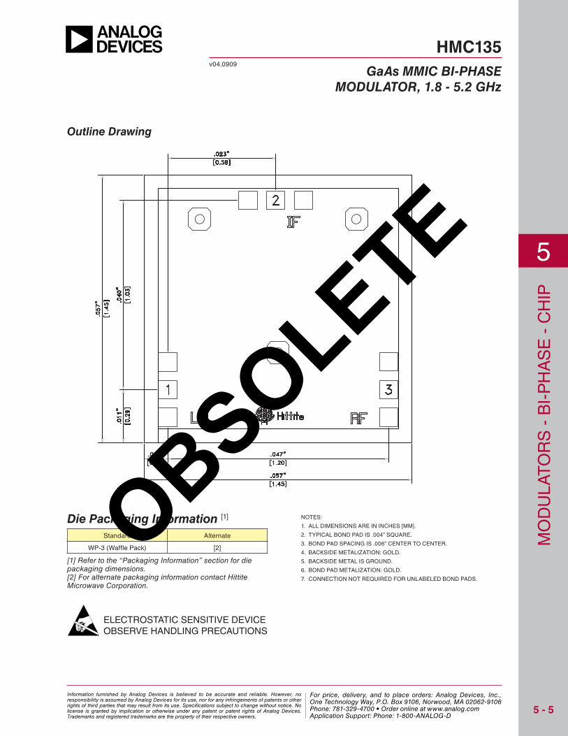
Outline Drawing
NOTES:
1. ALL DIMENSIONS ARE IN INCHES [MM].
2. TYPICAL BOND PAD IS .004” SQUARE.
3. BOND PAD SPACING IS .006” CENTER TO CENTER.
4. BACKSIDE METALIZATION: GOLD.
5. BACKSIDE METAL IS GROUND.
6. BOND PAD METALIZATION: GOLD.
7. CONNECTION NOT REQUIRED FOR UNLABELED BOND PADS.
Die Packaging Information [1]
Standard Alternate
WP-3 (Waffle Pack) [2]
[1] Refer to the “Packaging Information” section for die packaging dimensions.[2] For alternate packaging information contact Hittite Microwave Corporation.
ELECTROSTATIC SENSITIVE DEVICEOBSERVE HANDLING PRECAUTIONS
HMC135v04.0909
GaAs MMIC BI-PHASE
MODULATOR, 1.8 - 5.2 GHz
OBSOLETE
Information furnished by Analog Devices is believed to be accurate and reliable. However, no responsibility is assumed by Analog Devices for its use, nor for any infringements of patents or other rights of third parties that may result from its use. Specifications subject to change without notice. No license is granted by implication or otherwise under any patent or patent rights of Analog Devices. Trademarks and registered trademarks are the property of their respective owners.
For price, delivery, and to place orders: Analog Devices, Inc., One Technology Way, P.O. Box 9106, Norwood, MA 02062-9106 Phone: 781-329-4700 • Order online at www.analog.com Application Support: Phone: 1-800-ANALOG-D
MO
DU
LAT
OR
S -
BI-
PH
AS
E -
CH
IP
5
5 - 6
For price, delivery, and to place orders, please contact Hittite Microwave Corporation:20 Alpha Road, Chelmsford, MA 01824 Phone: 978-250-3343 Fax: 978-250-3373
Order On-line at www.hittite.com
HMC135v04.0909
GaAs MMIC BI-PHASE
MODULATOR, 1.8 - 5.2 GHz
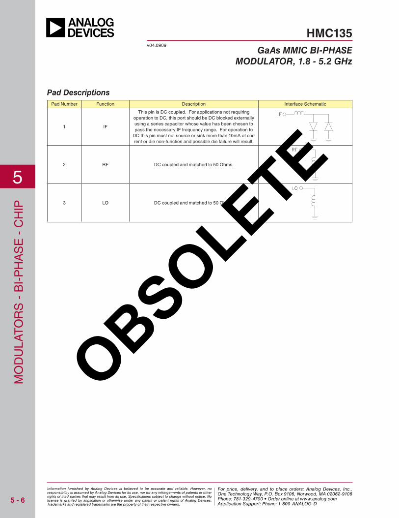
Pad Number Function Description Interface Schematic
1 IF
This pin is DC coupled. For applications not requiring operation to DC, this port should be DC blocked externally using a series capacitor whose value has been chosen to pass the necessary IF frequency range. For operation to
DC this pin must not source or sink more than 10mA of cur-rent or die non-function and possible die failure will result.
2 RF DC coupled and matched to 50 Ohms.
3 LO DC coupled and matched to 50 Ohms.
Pad Descriptions
OBSOLETE
Information furnished by Analog Devices is believed to be accurate and reliable. However, no responsibility is assumed by Analog Devices for its use, nor for any infringements of patents or other rights of third parties that may result from its use. Specifications subject to change without notice. No license is granted by implication or otherwise under any patent or patent rights of Analog Devices. Trademarks and registered trademarks are the property of their respective owners.
For price, delivery, and to place orders: Analog Devices, Inc., One Technology Way, P.O. Box 9106, Norwood, MA 02062-9106 Phone: 781-329-4700 • Order online at www.analog.com Application Support: Phone: 1-800-ANALOG-D
MO
DU
LAT
OR
S -
BI-
PH
AS
E -
CH
IP
5
5 - 7
For price, delivery, and to place orders, please contact Hittite Microwave Corporation:20 Alpha Road, Chelmsford, MA 01824 Phone: 978-250-3343 Fax: 978-250-3373
Order On-line at www.hittite.com
HMC135v04.0909
GaAs MMIC BI-PHASE
MODULATOR, 1.8 - 5.2 GHz
Mounting & Bonding Techniques for Millimeterwave GaAs MMICs
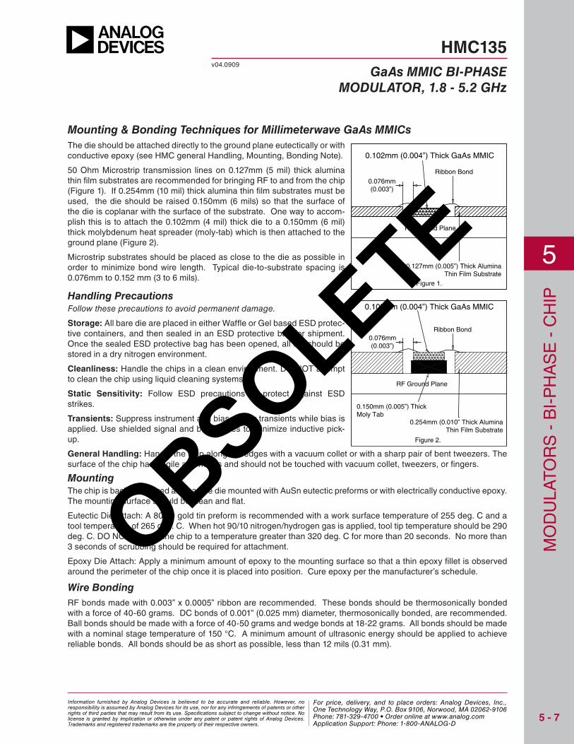
The die should be attached directly to the ground plane eutectically or with conductive epoxy (see HMC general Handling, Mounting, Bonding Note).
50 Ohm Microstrip transmission lines on 0.127mm (5 mil) thick alumina thin fi lm substrates are recommended for bringing RF to and from the chip (Figure 1). If 0.254mm (10 mil) thick alumina thin fi lm substrates must be used, the die should be raised 0.150mm (6 mils) so that the surface of the die is coplanar with the surface of the substrate. One way to accom-plish this is to attach the 0.102mm (4 mil) thick die to a 0.150mm (6 mil) thick molybdenum heat spreader (moly-tab) which is then attached to the ground plane (Figure 2).
Microstrip substrates should be placed as close to the die as possible in order to minimize bond wire length. Typical die-to-substrate spacing is 0.076mm to 0.152 mm (3 to 6 mils).
Handling PrecautionsFollow these precautions to avoid permanent damage.
Storage: All bare die are placed in either Waffle or Gel based ESD protec-tive containers, and then sealed in an ESD protective bag for shipment. Once the sealed ESD protective bag has been opened, all die should be stored in a dry nitrogen environment.
Cleanliness: Handle the chips in a clean environment. DO NOT attempt to clean the chip using liquid cleaning systems.
Static Sensitivity: Follow ESD precautions to protect against ESD strikes.
Transients: Suppress instrument and bias supply transients while bias is applied. Use shielded signal and bias cables to minimize inductive pick-up.
General Handling: Handle the chip along the edges with a vacuum collet or with a sharp pair of bent tweezers. The surface of the chip has fragile air bridges and should not be touched with vacuum collet, tweezers, or fi ngers.
MountingThe chip is back-metallized and can be die mounted with AuSn eutectic preforms or with electrically conductive epoxy. The mounting surface should be clean and fl at.
Eutectic Die Attach: A 80/20 gold tin preform is recommended with a work surface temperature of 255 deg. C and a tool temperature of 265 deg. C. When hot 90/10 nitrogen/hydrogen gas is applied, tool tip temperature should be 290 deg. C. DO NOT expose the chip to a temperature greater than 320 deg. C for more than 20 seconds. No more than 3 seconds of scrubbing should be required for attachment.
Epoxy Die Attach: Apply a minimum amount of epoxy to the mounting surface so that a thin epoxy fi llet is observed around the perimeter of the chip once it is placed into position. Cure epoxy per the manufacturer’s schedule.
Wire Bonding
RF bonds made with 0.003” x 0.0005” ribbon are recommended. These bonds should be thermosonically bonded with a force of 40-60 grams. DC bonds of 0.001” (0.025 mm) diameter, thermosonically bonded, are recommended. Ball bonds should be made with a force of 40-50 grams and wedge bonds at 18-22 grams. All bonds should be made with a nominal stage temperature of 150 °C. A minimum amount of ultrasonic energy should be applied to achieve reliable bonds. All bonds should be as short as possible, less than 12 mils (0.31 mm).
0.102mm (0.004”) Thick GaAs MMIC
Ribbon Bond0.076mm(0.003”)
RF Ground Plane
0.127mm (0.005”) Thick Alumina Thin Film Substrate
Figure 1.
0.102mm (0.004”) Thick GaAs MMIC
Ribbon Bond0.076mm(0.003”)
RF Ground Plane
0.150mm (0.005”) ThickMoly Tab
0.254mm (0.010” Thick AluminaThin Film Substrate
Figure 2.
OBSOLETE
Information furnished by Analog Devices is believed to be accurate and reliable. However, no responsibility is assumed by Analog Devices for its use, nor for any infringements of patents or other rights of third parties that may result from its use. Specifications subject to change without notice. No license is granted by implication or otherwise under any patent or patent rights of Analog Devices. Trademarks and registered trademarks are the property of their respective owners.
For price, delivery, and to place orders: Analog Devices, Inc., One Technology Way, P.O. Box 9106, Norwood, MA 02062-9106 Phone: 781-329-4700 • Order online at www.analog.com Application Support: Phone: 1-800-ANALOG-D