Embed Size (px)
Citation preview
TUSB1105, TUSB1106
www.ti.com SCAS818E –MAY 2006–REVISED SEPTEMBER 2010
ADVANCED UNIVERSAL SERIAL BUS TRANSCEIVERSCheck for Samples: TUSB1105, TUSB1106
1FEATURES • Support I/O Voltage Range From 1.65 V to3.6 V• Compatible With Universal Serial Bus
Specification Rev. 2.0 • IEC-61000-4-2 ESD Compliant• Transmit and Receive Serial Data at Both – ±9-kV Contact-Discharge Model
Full-Speed (12-Mbit/s) and Low-Speed (D+, D–, VCC(5.0))(1.5-Mbit/s) Data Rates – ±15-kV Human-Body Model
• Integrated Bypassable 5-V to 3.3-V Voltage (D+, D–, VCC(5.0))Regulator for Powering Via USB VBUS • TUSB1105 Available in Quad Flat No-Lead
• VBUS Disconnection Indication Through VP and (QFN) Package; TUSB1106 Available in QFNVM and Thin Shrink Small-Outline Package
(TSSOP)• Used as USB Device Transceiver or USB HostTransceiver
APPLICATIONS• Stable RCV Output During SE0 Condition• Mobile Phones• Two Single-Ended Receivers With Hysteresis• Personal Digital Assistants (PDAs)
• Low-Power Operation, Ideal for Portable• Information Appliances (IAs)Equipment• Digital Still Cameras (DSCs)
DESCRIPTION/ORDERING INFORMATIONThe TUSB1105 and TUSB1106 universal serial bus (USB) transceivers are compliant with the Universal SerialBus Specification Rev. 2.0. These devices can transmit and receive serial data at both full-speed (12-Mbit/s) andlow-speed (1.5-Mbit/s) data rates. The TUSB1105 and TUSB1106 can be used as USB device transceivers orUSB host transceivers.
The devices allow USB application-specific ICs (ASICs) and programmable logic devices (PLDs), withpower-supply voltages from 1.65 V to 3.6 V, to interface with the physical layer (PHY) of the universal serial bus.They have an integrated 5-V to 3.3-V voltage regulator for direct powering via the USB supply VBUS.
The TUSB1105 allows single-ended and differential input modes selectable by a mode (MODE) input and isavailable in RGT and RTZ packages. The TUSB1106 allows only differential input mode and is available in PW,RGT, RSV, and RTZ packages.
The TUSB1105 and TUSB1106 are ideal for portable electronic devices, such as mobile phones, personal digitalassistants, information appliances, and digital still cameras.
ORDERING INFORMATIONTA PACKAGE (1) (2) ORDERABLE PART NUMBER TOP-SIDE MARKING
TUSB1105RGTR ZYBQFN – RGT Reel of 3000
TUSB1106RGTR ZYC
TUSB1105RTZR ZYB–40°C to 85°C QFN – RTZ Reel of 3000
TUSB1106RTZR ZYC
QFN – RSV Reel of 3000 TUSB1106RSVR ZYC
TSSOP – PW Reel of 2000 TUSB1106PWR TU1106
(1) Package drawings, thermal data, and symbolization are available at www.ti.com/packaging.(2) For the most current package and ordering information, see the Package Option Addendum at the end of this document, or see the TI
website at www.ti.com.
1
Please be aware that an important notice concerning availability, standard warranty, and use in critical applications of TexasInstruments semiconductor products and disclaimers thereto appears at the end of this data sheet.
PRODUCTION DATA information is current as of publication date. Copyright © 2006–2010, Texas Instruments IncorporatedProducts conform to specifications per the terms of the TexasInstruments standard warranty. Production processing does notnecessarily include testing of all parameters.
D−
D+
MO
DE
SU
SP
ND
VPO/VO
VMO/FSE0
8
GND(exposed die pad)
VC
C(I
/O)
5 6 7
4
3
2
9
10
11
13141516
SP
EE
D
1 12
RCV
VP
OE
VM
Vp
u(3
.3)
SO
FT
CO
N
VC
C(5
.0)
Vre
g(3
.3)
SO
FT
CO
N
Vp
u(3
.3)
RCV
VP
OE
D+
D−
SP
EE
D
VC
C(I
/O)
VPO/VO
VM
SUSPND
MO
DE
VC
C(5
.0)
Vreg(3.3)
VMO/FSE0
13141516
876
12
11
10
9
2
1
3
4
5
G ND(exposed die pad)
D−
D+
GN
D
SU
SP
ND
VPO
VMO
8
No Connect
VC
C(I
/O)
5 6 7
4
3
2
9
10
11
13141516
SP
EE
D
1 12
RCV
VP
OE
VM
Vp
u(3
.3)
SO
FT
CO
N
VC
C(5
.0)
Vre
g(3
.3)
SO
FT
CO
N
Vp
u(3
.3)
RCV
VP
O E
D+
D−
SP
EE
D
VC
C(I
/O)
VPO
VM
SUSPND
GN
D
VC
C(5
.0)
Vreg(3.3)
VMO
13141516
876
12
11
10
9
2
1
3
4
5
SO
FT
CO
N
VP
U(3
.3)
VM
VP
RCV
OE
D-
D+
VPO
VMO
SU
SP
ND
GN
D
VC
C(I
/O)
SP
EE
D
VC
C(5
.0)
Vre
g(3
.3)
1
2
3
4
5
6
7
8
16
15
14
13
12
11
10
9
Vpu(3 .3)
SO FTCO N
O E
R CV
VP
VM
SUSPN D
GN D V C C ( I /O )
SPEED
D −
D +
VPO
VM O
Vreg(3 .3 )
VCC (5 .0 )
TUSB1105, TUSB1106
SCAS818E –MAY 2006–REVISED SEPTEMBER 2010 www.ti.com
TUSB1105 PACKAGESRGT PACKAGE RTZ PACKAGE(BOTTOM VIEW) (BOTTOM VIEW)
TUSB1106 PACKAGESRGT PACKAGE RTZ PACKAGE(BOTTOM VIEW) (BOTTOM VIEW)
RSV PACKAGE PW PACKAGE(BOTTOM VIEW) (TOP VIEW)
2 Submit Documentation Feedback Copyright © 2006–2010, Texas Instruments Incorporated
Product Folder Link(s): TUSB1105 TUSB1106
M B L 3 0 1
VCC(I/O)
SOFTCON
OE
SPEEDVMO/FSE0(B)
VPO/VO(B)
MODE(C)
SUSPND
RCV
VP
VM
LevelShifter
VoltageRegulator
GND
33 (1%)
33 (1%)
3.3 V
Vpu(3.3)
Vreg(3.3)
VCC(5.0)
1.5 kΩ(A)
D+
D–
TUSB1105TUSB1106
+
–
TUSB1105, TUSB1106
www.ti.com SCAS818E –MAY 2006–REVISED SEPTEMBER 2010
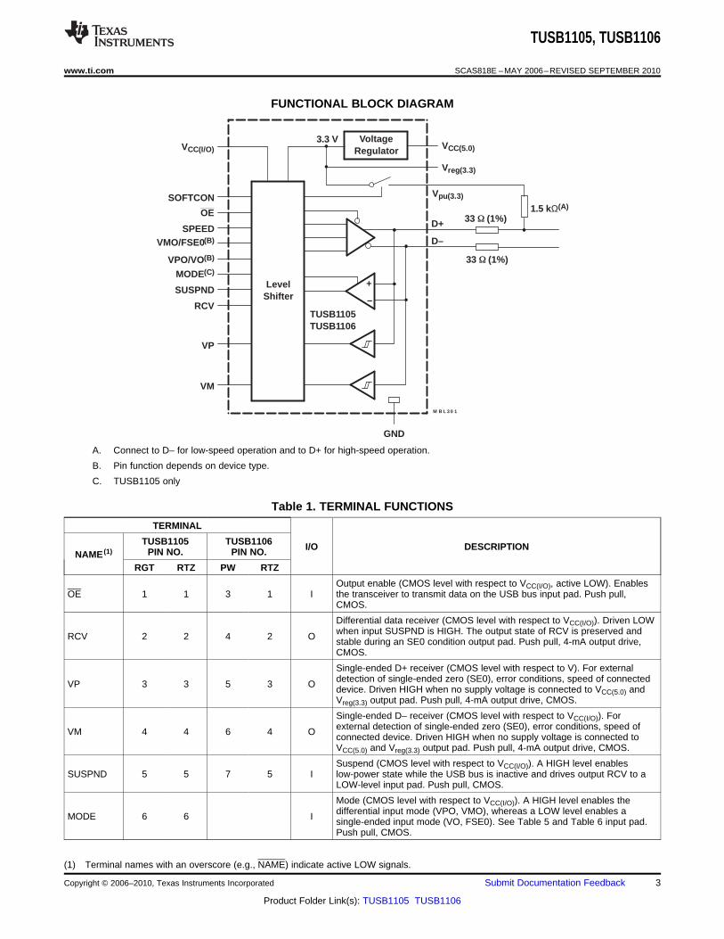
FUNCTIONAL BLOCK DIAGRAM
A. Connect to D– for low-speed operation and to D+ for high-speed operation.
B. Pin function depends on device type.
C. TUSB1105 only
Table 1. TERMINAL FUNCTIONS
TERMINAL
TUSB1105 TUSB1106 I/O DESCRIPTIONPIN NO. PIN NO.NAME (1)
RGT RTZ PW RTZ
Output enable (CMOS level with respect to VCC(I/O), active LOW). EnablesOE 1 1 3 1 I the transceiver to transmit data on the USB bus input pad. Push pull,
CMOS.
Differential data receiver (CMOS level with respect to VCC(I/O)). Driven LOWwhen input SUSPND is HIGH. The output state of RCV is preserved andRCV 2 2 4 2 O stable during an SE0 condition output pad. Push pull, 4-mA output drive,CMOS.
Single-ended D+ receiver (CMOS level with respect to V). For externaldetection of single-ended zero (SE0), error conditions, speed of connectedVP 3 3 5 3 O device. Driven HIGH when no supply voltage is connected to VCC(5.0) andVreg(3.3) output pad. Push pull, 4-mA output drive, CMOS.
Single-ended D– receiver (CMOS level with respect to VCC(I/O)). Forexternal detection of single-ended zero (SE0), error conditions, speed ofVM 4 4 6 4 O connected device. Driven HIGH when no supply voltage is connected toVCC(5.0) and Vreg(3.3) output pad. Push pull, 4-mA output drive, CMOS.
Suspend (CMOS level with respect to VCC(I/O)). A HIGH level enablesSUSPND 5 5 7 5 I low-power state while the USB bus is inactive and drives output RCV to a
LOW-level input pad. Push pull, CMOS.
Mode (CMOS level with respect to VCC(I/O)). A HIGH level enables thedifferential input mode (VPO, VMO), whereas a LOW level enables aMODE 6 6 I single-ended input mode (VO, FSE0). See Table 5 and Table 6 input pad.Push pull, CMOS.
(1) Terminal names with an overscore (e.g., NAME) indicate active LOW signals.
Copyright © 2006–2010, Texas Instruments Incorporated Submit Documentation Feedback 3
Product Folder Link(s): TUSB1105 TUSB1106
TUSB1105, TUSB1106
SCAS818E –MAY 2006–REVISED SEPTEMBER 2010 www.ti.com
Table 1. TERMINAL FUNCTIONS (continued)
TERMINAL
TUSB1105 TUSB1106 I/O DESCRIPTIONPIN NO. PIN NO.NAME (1)
RGT RTZ PW RTZ
GND Die pad Die pad 8 6 Ground supply (2)
Supply voltage for digital I/O pins (1.65 to 3.6 V). When VCC(I/O) is notconnected, the D+ and D– pins are in 3-state. This supply pin isVCC(I/O) 7 7 9 7 independent of VCC(5.0) and Vreg(3.3) and must never exceed the Vreg(3.3)voltage.
Speed selection (CMOS level with respect to VCC(I/O)). Adjusts the slew rateof differential data outputs D+ and D– according to the transmission speed.
SPEED 8 8 10 8 I Input pad, push pull, CMOS.LOW – low speed (1.5 Mbit/s)HIGH – full speed (12 Mbit/s)
Negative USB data bus connection (analog, differential). For low-speedD– 9 9 11 9 AI/O mode, connect to pin Vpu(3.3) via a 1.5-kΩ resistor.
Positive USB data bus connection (analog, differential). For full-speedD+ 10 10 12 10 AI/O mode, connect to pin Vpu(3.3) via a 1.5-kΩ resistor.
VPO/VO 11 11 I Driver data (CMOS level with respect to VCC(I/O), Schmitt trigger). SeeDriving Function Table (pin OE = L) using single-ended input data interfacefor TUSB1105 (pin MODE = L), and Driving Function Table (pin OE = L)
VPO 13 11 using differential input data interface for TUSB1105 (pin MODE = H) andTUSB1106 input pad. Push pull, CMOS.
VMO/FSE0 12 12 I Driver data (CMOS level with respect to VCC(I/O), Schmitt trigger). SeeDriving Function Table (pin OE = L) using single-ended input data interfacefor TUSB1105 (pin MODE = L), and Driving Function Table (pin OE = L)
VMO 14 12 using differential input data interface for TUSB1105 (pin MODE = H) andTUSB1106 input pad. Push pull, CMOS.
Internal regulator option. Regulated supply-voltage output (3 V to 3.6 V)during 5-V operation. A decoupling capacitor of at least 0.1 mF is requiredVreg(3.3) 13 13 15 13 for the regulator bypass option. Used as a supply-voltage input for3.3 V ± 10% operation.
Internal regulator option. Supply-voltage input (4 V to 5.5 V). Can beVCC(5.0) 14 14 16 14 connected directly to USB supply VBUS regulator bypass option. Connect
to Vreg(3.3).
Pullup supply voltage (3.3 V ± 10%). Connect an external 1.5-kΩ resistor onD+ (full speed) or D– (low speed). Pin function is controlled by inputSOFTCON.Vpu(3.3) 15 15 1 15 SOFTCON = LOW – Vpu(3.3) floating (high impedance), ensures zero pullupcurrentSOFTCON = HIGH – Vpu(3.3) = 3.3 V, internally connected to Vreg(3.3)
Software-controlled USB connection. A HIGH level applies 3.3 V to pinVpu(3.3), which is connected to an external 1.5-kΩ pullup resistor. This allowsSOFTCON 16 16 2 16 I USB connect/disconnect signaling to be controlled by software input pad.Push pull, CMOS.
(2) TUSB1105 ground terminal is connected to the exposed die pad (heat sink). The package die pad is open on the TUSB1106.
4 Submit Documentation Feedback Copyright © 2006–2010, Texas Instruments Incorporated
Product Folder Link(s): TUSB1105 TUSB1106
TUSB1105, TUSB1106
www.ti.com SCAS818E –MAY 2006–REVISED SEPTEMBER 2010
FUNCTIONAL DESCRIPTION
Function Selection
Table 2. FUNCTION TABLE
SUSPND OE D+, D– RCV VP, VM FUNCTION
L L Driving and receiving Active Active Normal driving (differential receiver active)
L H Receiving (1) Active Active Receiving
H L Driving Inactive (2) Active Driving during suspend (3) (differential receiver inactive)
H H High-Z (1) Inactive (2) Active Low-power state
(1) Signal levels on D+ and D– are determined by other USB devices and external pullup/pulldown resistors.(2) In suspend mode (SUSPND = HIGH) the differential receiver is inactive and output RCV is always LOW. Out of suspend (K), signaling is
detected via the single-ended receivers VP and VM.(3) During suspend, the slew-rate control circuit of low-speed operation is disabled. The D+ and D– lines are still driven to their intended
states, without slew-rate control. This is permitted because driving during suspend is used to signal remote wakeup by driving a K signal(one transition from idle to K state) for a period of 1 ms to 15 ms.
Operating Functions
Table 3. FUNCTION TABLESxxx
Driving Function (Pin OE = L)Using Single-Ended Input Data Interface
for TUSB1105 (Pin MODE = L)
DATA STATEFSE0 VO DATA
LOW SPEED FULL SPEED
L L Differential logic 0 J K
L H Differential logic 1 K J
H L SE0 X X
H H SE0 X X
Table 4. Driving Function (Pin OE = L)Using Differential Input Data Interface
for TUSB1105 (Pin MODE = H) and TUSB1106
DATA STATEVMO VPO DATA
LOW SPEED FULL SPEED
L L SE0 X X
H L Differential logic 0 J K
L H Differential logic 1 K J
H H Illegal state X X
Copyright © 2006–2010, Texas Instruments Incorporated Submit Documentation Feedback 5
Product Folder Link(s): TUSB1105 TUSB1106
TUSB1105, TUSB1106
SCAS818E –MAY 2006–REVISED SEPTEMBER 2010 www.ti.com
Table 5. Receiving Function (Pin OE = H)
DATA STATED+, D– RCV VP (1) VM (1)
LOW FULLSPEED SPEED
Differential L L H J Klogic 0
Differential H H L K Jlogic 1
SE0 RCV* (2) L L X X
(1) VP = VM = H indicates the sharing mode (VCC(5.0) and Vreg(3.3) aredisconnected).
(2) RCV* denotes the signal level on output RCV just before SE0 stateoccurs. This level is stable during the SE0 period.
Power-Supply Configurations
The TUSB1105/1106 can be used with different power-supply configurations, which can be dynamically changed.An overview is given in Table 7.• Normal mode – Both VCC(I/O) and VCC(5.0) or (VCC(5.0) and Vreg(3.3)) are connected. For 5-V operation, VCC(5.0) is
connected to a 5-V source (4 V to 5.5 V). The internal voltage regulator then produces 3.3 V for the USBconnections. For 3.3-V operation, both VCC(5.0) and Vreg(3.3) are connected to a 3.3-V source (3 V to 3.6 V).VCC(I/O) is independently connected to a voltage source (1.65 V to 3.6 V), depending on the supply voltage ofthe external circuit.
• Disable mode – VCC(I/O) is not connected, VCC(5.0) or (VCC(5.0) and Vreg(3.3)) are connected. In this mode, theinternal circuits of the TUSB1105 and TUSB1106 ensure that the D+ and D– pins are in 3-state and thepower consumption drops to the low-power (suspended) state level. Some hysteresis is built into thedetection of VCC(I/O) lost.
• Sharing mode – VCC(I/O) is connected, (VCC(5.0) and Vreg(3.3)) are not connected. In this mode, the D+ and D–pins are made 3-state and the TUSB1105 and TUSB1106 allow external signals of up to 3.6 V to share theD+ and D– lines. The internal circuits of the TUSB1105 and TUSB1106 ensure that virtually no current(maximum 10 mA) is drawn via the D+ and D– lines. The power consumption through VCC(I/O) drops to thelow-power (suspended) state level. Both the VP and VM pins are driven HIGH to indicate this mode. Pin RCVis made LOW. Some hysteresis is built into the detection of Vreg(3.3) lost.
Table 6. Pin States in Disable or Sharing Mode
PINS DISABLE-MODE STATE SHARING-MODE STATE
VCC(5.0)/Vreg(3.3) 5-V input/3.3-V output, 3.3-V input/3.3-V input Not present
VCC(I/O) Not present 1.65-V to 3.6-V input
Vpu(3.3) High impedance (off) High impedance (off)
D+, D– High impedance High impedance
VP, VM Invalid (1) H
RCV Invalid (1) L
Inputs (VO/VPO, FSE0/VMO, SPEED, High impedance High impedanceMODE (2), SUSPND, OE, SOFTCON)
(1) High impedance or driven LOW(2) TUSB1105 only
Table 7. Power-Supply Configuration Overview
VCC(5.0) or Vreg(3.3) VCC(I/O) CONFIGURATION SPECIAL CHARACTERISTICS
Connected Connected Normal mode
D+, D–, and Vpu(3.3) are in high impedance.Connected Not connected Disable mode VP, VM, and RCV are invalid. (1)
D+, D–, and Vpu(3.3) are in high impedance.Not connected Connected Sharing mode VP and VM are driven HIGH. RCV is driven LOW.
(1) High impedance or driven LOW
6 Submit Documentation Feedback Copyright © 2006–2010, Texas Instruments Incorporated
Product Folder Link(s): TUSB1105 TUSB1106
TUSB1105, TUSB1106
www.ti.com SCAS818E –MAY 2006–REVISED SEPTEMBER 2010
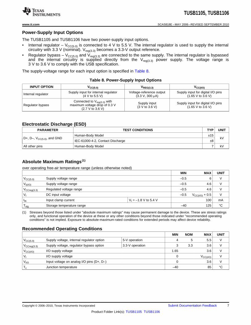
Power-Supply Input Options
The TUSB1105 and TUSB1106 have two power-supply input options.• Internal regulator – VCC(5.0) is connected to 4 V to 5.5 V. The internal regulator is used to supply the internal
circuitry with 3.3 V (nominal). Vreg(3.3) becomes a 3.3-V output reference.• Regulator bypass – VCC(5.0) and Vreg(3.3) are connected to the same supply. The internal regulator is bypassed
and the internal circuitry is supplied directly from the Vreg(3.3) power supply. The voltage range is3 V to 3.6 V to comply with the USB specification.
The supply-voltage range for each input option is specified in Table 8.
Table 8. Power-Supply Input Options
INPUT OPTION VCC(5.0) VREG(3.3) VCC(I/O)
Supply input for internal regulator Voltage-reference output Supply input for digital I/O pinsInternal regulator (4 V to 5.5 V) (3.3 V, 300 mA) (1.65 V to 3.6 V)
Connected to Vreg(3.3) with Supply input Supply input for digital I/O pinsRegulator bypass maximum voltage drop of 0.3 V (3 V to 3.6 V) (1.65 V to 3.6 V)(2.7 V to 3.6 V)
Electrostatic Discharge (ESD)PARAMETER TEST CONDITIONS TYP UNIT
Human-Body Model ±15D+, D–, VCC(5.0), and GND kV
IEC-61000-4-2, Contact Discharge ±8
All other pins Human-Body Model 7 kV
Absolute Maximum Ratings (1)
over operating free-air temperature range (unless otherwise noted)MIN MAX UNIT
VCC(5.0) Supply voltage range –0.5 6 V
VI(I/O) Supply voltage range –0.5 4.6 V
VCCreg(3.3) Regulated voltage range –0.5 4.6 V
VI DC input voltage –0.5 VCC(I/O) + 0.5 V
IIK Input clamp current VI = –1.8 V to 5.4 V 100 mA
Tstg Storage temperature range –40 125 °C
(1) Stresses beyond those listed under "absolute maximum ratings" may cause permanent damage to the device. These are stress ratingsonly, and functional operation of the device at these or any other conditions beyond those indicated under "recommended operatingconditions" is not implied. Exposure to absolute-maximum-rated conditions for extended periods may affect device reliability.
Recommended Operating ConditionsMIN NOM MAX UNIT
VCC(5.0) Supply voltage, internal regulator option 5-V operation 4 5 5.5 V
VCCreg(3.3) Supply voltage, regulator bypass option 3.3-V operation 3 3.3 3.6 V
VCC(I/O) I/O supply voltage 1.65 3.6 V
VI I/O supply voltage 0 VCC(I/O) V
VI/O Input voltage on analog I/O pins (D+, D–) 0 3.6 V
Tc Junction temperature –40 85 °C
Copyright © 2006–2010, Texas Instruments Incorporated Submit Documentation Feedback 7
Product Folder Link(s): TUSB1105 TUSB1106
TUSB1105, TUSB1106
SCAS818E –MAY 2006–REVISED SEPTEMBER 2010 www.ti.com
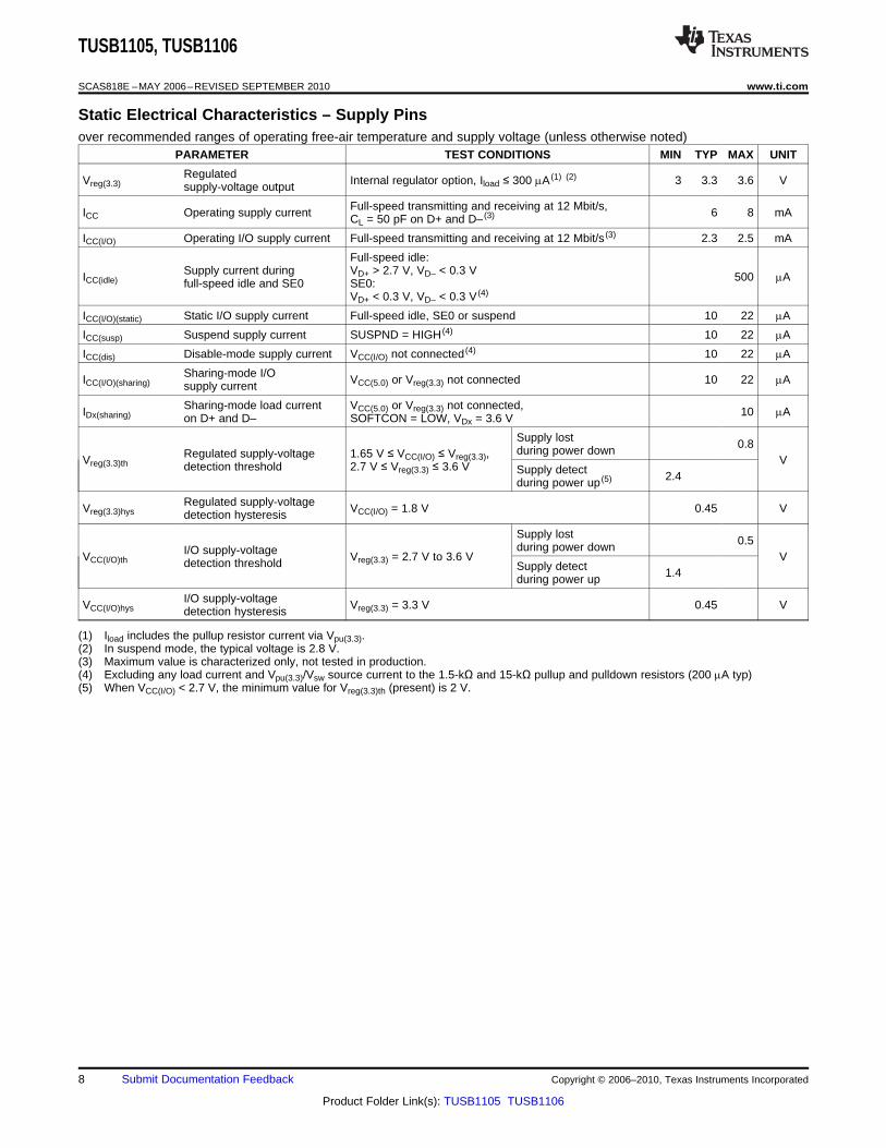
Static Electrical Characteristics – Supply Pinsover recommended ranges of operating free-air temperature and supply voltage (unless otherwise noted)
PARAMETER TEST CONDITIONS MIN TYP MAX UNIT
RegulatedVreg(3.3) Internal regulator option, Iload ≤ 300 mA (1) (2) 3 3.3 3.6 Vsupply-voltage output
Full-speed transmitting and receiving at 12 Mbit/s,ICC Operating supply current 6 8 mACL = 50 pF on D+ and D– (3)
ICC(I/O) Operating I/O supply current Full-speed transmitting and receiving at 12 Mbit/s (3) 2.3 2.5 mA
Full-speed idle:Supply current during VD+ > 2.7 V, VD– < 0.3 VICC(idle) 500 mAfull-speed idle and SE0 SE0:
VD+ < 0.3 V, VD– < 0.3 V (4)
ICC(I/O)(static) Static I/O supply current Full-speed idle, SE0 or suspend 10 22 mA
ICC(susp) Suspend supply current SUSPND = HIGH (4) 10 22 mA
ICC(dis) Disable-mode supply current VCC(I/O) not connected (4) 10 22 mA
Sharing-mode I/OICC(I/O)(sharing) VCC(5.0) or Vreg(3.3) not connected 10 22 mAsupply current
Sharing-mode load current VCC(5.0) or Vreg(3.3) not connected,IDx(sharing) 10 mAon D+ and D– SOFTCON = LOW, VDx = 3.6 V
Supply lost 0.8during power downRegulated supply-voltage 1.65 V ≤ VCC(I/O) ≤ Vreg(3.3),Vreg(3.3)th Vdetection threshold 2.7 V ≤ Vreg(3.3) ≤ 3.6 V Supply detect 2.4during power up (5)
Regulated supply-voltageVreg(3.3)hys VCC(I/O) = 1.8 V 0.45 Vdetection hysteresis
Supply lost 0.5during power downI/O supply-voltageVCC(I/O)th Vreg(3.3) = 2.7 V to 3.6 V Vdetection threshold Supply detect 1.4during power up
I/O supply-voltageVCC(I/O)hys Vreg(3.3) = 3.3 V 0.45 Vdetection hysteresis
(1) Iload includes the pullup resistor current via Vpu(3.3).(2) In suspend mode, the typical voltage is 2.8 V.(3) Maximum value is characterized only, not tested in production.(4) Excluding any load current and Vpu(3.3)/Vsw source current to the 1.5-kΩ and 15-kΩ pullup and pulldown resistors (200 mA typ)(5) When VCC(I/O) < 2.7 V, the minimum value for Vreg(3.3)th (present) is 2 V.
8 Submit Documentation Feedback Copyright © 2006–2010, Texas Instruments Incorporated
Product Folder Link(s): TUSB1105 TUSB1106
TUSB1105, TUSB1106
www.ti.com SCAS818E –MAY 2006–REVISED SEPTEMBER 2010
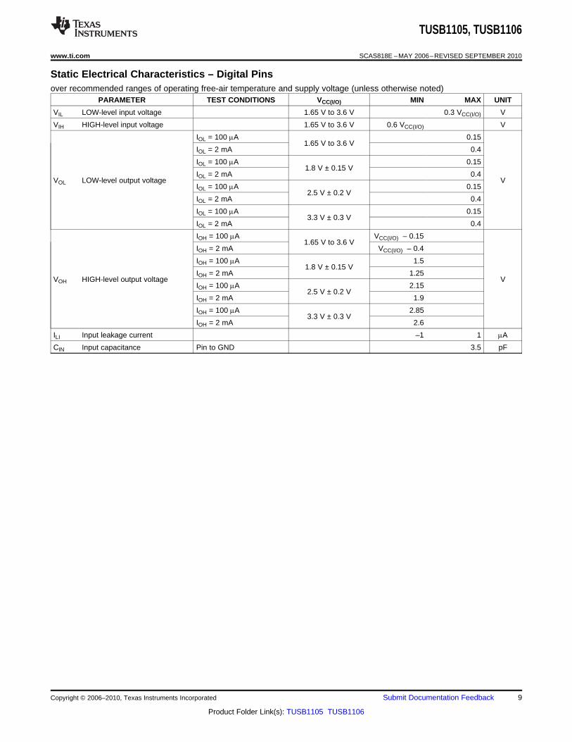
Static Electrical Characteristics – Digital Pinsover recommended ranges of operating free-air temperature and supply voltage (unless otherwise noted)
PARAMETER TEST CONDITIONS VCC(I/O) MIN MAX UNIT
VIL LOW-level input voltage 1.65 V to 3.6 V 0.3 VCC(I/O) V
VIH HIGH-level input voltage 1.65 V to 3.6 V 0.6 VCC(I/O) V
IOL = 100 mA 0.151.65 V to 3.6 V
IOL = 2 mA 0.4
IOL = 100 mA 0.151.8 V ± 0.15 V
IOL = 2 mA 0.4VOL LOW-level output voltage V
IOL = 100 mA 0.152.5 V ± 0.2 V
IOL = 2 mA 0.4
IOL = 100 mA 0.153.3 V ± 0.3 V
IOL = 2 mA 0.4
IOH = 100 mA VCC(I/O) – 0.151.65 V to 3.6 V
IOH = 2 mA VCC(I/O) – 0.4
IOH = 100 mA 1.51.8 V ± 0.15 V
IOH = 2 mA 1.25VOH HIGH-level output voltage V
IOH = 100 mA 2.152.5 V ± 0.2 V
IOH = 2 mA 1.9
IOH = 100 mA 2.853.3 V ± 0.3 V
IOH = 2 mA 2.6
ILI Input leakage current –1 1 mA
CIN Input capacitance Pin to GND 3.5 pF
Copyright © 2006–2010, Texas Instruments Incorporated Submit Documentation Feedback 9
Product Folder Link(s): TUSB1105 TUSB1106
TUSB1105, TUSB1106
SCAS818E –MAY 2006–REVISED SEPTEMBER 2010 www.ti.com
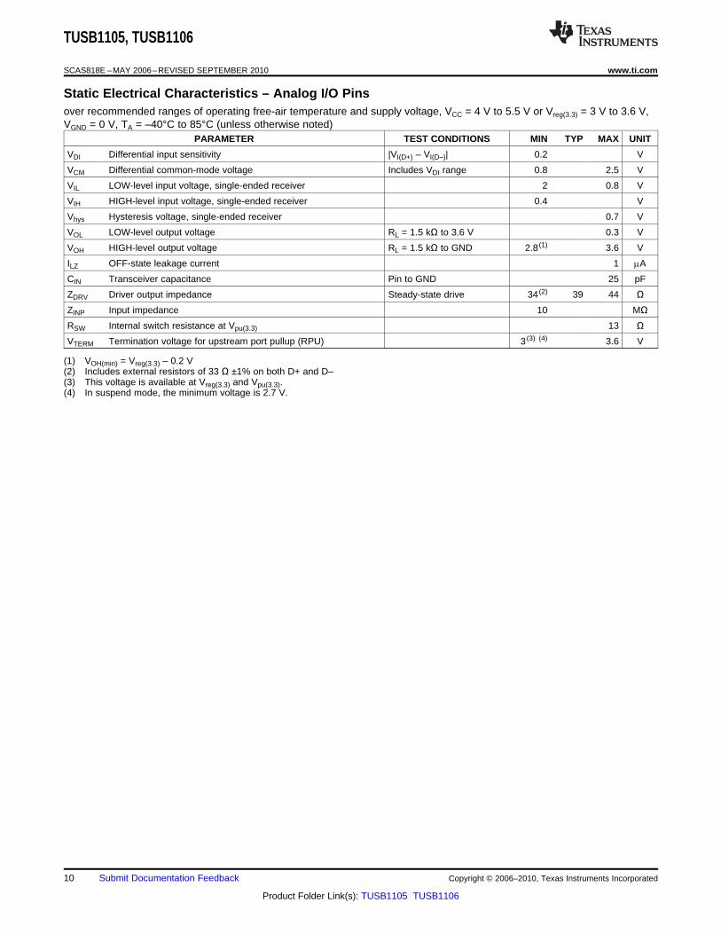
Static Electrical Characteristics – Analog I/O Pinsover recommended ranges of operating free-air temperature and supply voltage, VCC = 4 V to 5.5 V or Vreg(3.3) = 3 V to 3.6 V,VGND = 0 V, TA = –40°C to 85°C (unless otherwise noted)
PARAMETER TEST CONDITIONS MIN TYP MAX UNIT
VDI Differential input sensitivity |VI(D+) – VI(D–)| 0.2 V
VCM Differential common-mode voltage Includes VDI range 0.8 2.5 V
VIL LOW-level input voltage, single-ended receiver 2 0.8 V
VIH HIGH-level input voltage, single-ended receiver 0.4 V
Vhys Hysteresis voltage, single-ended receiver 0.7 V
VOL LOW-level output voltage RL = 1.5 kΩ to 3.6 V 0.3 V
VOH HIGH-level output voltage RL = 1.5 kΩ to GND 2.8 (1) 3.6 V
ILZ OFF-state leakage current 1 mA
CIN Transceiver capacitance Pin to GND 25 pF
ZDRV Driver output impedance Steady-state drive 34 (2) 39 44 ΩZINP Input impedance 10 MΩRSW Internal switch resistance at Vpu(3.3) 13 ΩVTERM Termination voltage for upstream port pullup (RPU) 3 (3) (4) 3.6 V
(1) VOH(min) = Vreg(3.3) – 0.2 V(2) Includes external resistors of 33 Ω ±1% on both D+ and D–(3) This voltage is available at Vreg(3.3) and Vpu(3.3).(4) In suspend mode, the minimum voltage is 2.7 V.
10 Submit Documentation Feedback Copyright © 2006–2010, Texas Instruments Incorporated
Product Folder Link(s): TUSB1105 TUSB1106
TUSB1105, TUSB1106
www.ti.com SCAS818E –MAY 2006–REVISED SEPTEMBER 2010
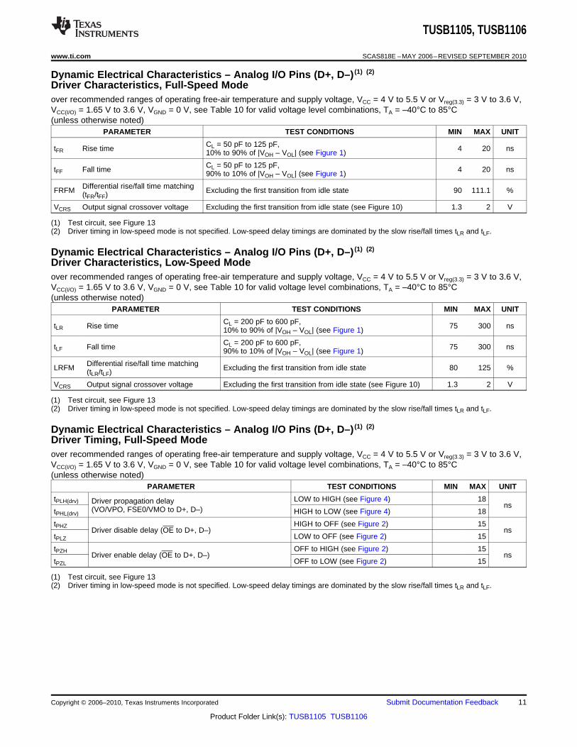
Dynamic Electrical Characteristics – Analog I/O Pins (D+, D–) (1) (2)
Driver Characteristics, Full-Speed Modeover recommended ranges of operating free-air temperature and supply voltage, VCC = 4 V to 5.5 V or Vreg(3.3) = 3 V to 3.6 V,VCC(I/O) = 1.65 V to 3.6 V, VGND = 0 V, see Table 10 for valid voltage level combinations, TA = –40°C to 85°C(unless otherwise noted)
PARAMETER TEST CONDITIONS MIN MAX UNIT
CL = 50 pF to 125 pF,tFR Rise time 4 20 ns10% to 90% of |VOH – VOL| (see Figure 1)
CL = 50 pF to 125 pF,tFF Fall time 4 20 ns90% to 10% of |VOH – VOL| (see Figure 1)
Differential rise/fall time matchingFRFM Excluding the first transition from idle state 90 111.1 %(tFR/tFF)
VCRS Output signal crossover voltage Excluding the first transition from idle state (see Figure 10) 1.3 2 V
(1) Test circuit, see Figure 13(2) Driver timing in low-speed mode is not specified. Low-speed delay timings are dominated by the slow rise/fall times tLR and tLF.
Dynamic Electrical Characteristics – Analog I/O Pins (D+, D–) (1) (2)
Driver Characteristics, Low-Speed Modeover recommended ranges of operating free-air temperature and supply voltage, VCC = 4 V to 5.5 V or Vreg(3.3) = 3 V to 3.6 V,VCC(I/O) = 1.65 V to 3.6 V, VGND = 0 V, see Table 10 for valid voltage level combinations, TA = –40°C to 85°C(unless otherwise noted)
PARAMETER TEST CONDITIONS MIN MAX UNIT
CL = 200 pF to 600 pF,tLR Rise time 75 300 ns10% to 90% of |VOH – VOL| (see Figure 1)
CL = 200 pF to 600 pF,tLF Fall time 75 300 ns90% to 10% of |VOH – VOL| (see Figure 1)
Differential rise/fall time matchingLRFM Excluding the first transition from idle state 80 125 %(tLR/tLF)
VCRS Output signal crossover voltage Excluding the first transition from idle state (see Figure 10) 1.3 2 V
(1) Test circuit, see Figure 13(2) Driver timing in low-speed mode is not specified. Low-speed delay timings are dominated by the slow rise/fall times tLR and tLF.
Dynamic Electrical Characteristics – Analog I/O Pins (D+, D–) (1) (2)
Driver Timing, Full-Speed Modeover recommended ranges of operating free-air temperature and supply voltage, VCC = 4 V to 5.5 V or Vreg(3.3) = 3 V to 3.6 V,VCC(I/O) = 1.65 V to 3.6 V, VGND = 0 V, see Table 10 for valid voltage level combinations, TA = –40°C to 85°C(unless otherwise noted)
PARAMETER TEST CONDITIONS MIN MAX UNIT
tPLH(drv) LOW to HIGH (see Figure 4) 18Driver propagation delay ns(VO/VPO, FSE0/VMO to D+, D–)tPHL(drv) HIGH to LOW (see Figure 4) 18
tPHZ HIGH to OFF (see Figure 2) 15Driver disable delay (OE to D+, D–) ns
tPLZ LOW to OFF (see Figure 2) 15
tPZH OFF to HIGH (see Figure 2) 15Driver enable delay (OE to D+, D–) ns
tPZL OFF to LOW (see Figure 2) 15
(1) Test circuit, see Figure 13(2) Driver timing in low-speed mode is not specified. Low-speed delay timings are dominated by the slow rise/fall times tLR and tLF.
Copyright © 2006–2010, Texas Instruments Incorporated Submit Documentation Feedback 11
Product Folder Link(s): TUSB1105 TUSB1106
MGS963
10%
90% 90%
10%VOL
VOH
tFR,tLR tFF,tLF
MGS966
Logic Input
DifferentialData Lines
1.8 V
0 V
VOH
VOL
0.9 V 0.9 V
VOL + 0.3 V
VOH − 0.3 VVCRS
tPZHtPZL
tPHZtPLZ
MGS964VOL
Logic Output
VOH
DifferentialData Lines
0.9 V
VCRS VCRS
1.8 V
0 VtPLH(drv) tPHL(drv)
0.9 V
MGS965VOL
Logic Output
VOH
0.8 V
DifferentialData Lines
2.0 V
VCRS
0.9 V 0.9 V
VCRS
tPLH(rcv)tPLH(se)
tPHL(rcv)tPHL(se)
TUSB1105, TUSB1106
SCAS818E –MAY 2006–REVISED SEPTEMBER 2010 www.ti.com
Dynamic Electrical Characteristics for Analog I/O Pins (D+, D–) (1)
Receiver Timing, Full-Speed and Low-Speed Mode, Differential Receiverover recommended ranges of operating free-air temperature and supply voltage, VCC = 4 V to 5.5 V or Vreg(3.3) = 3 V to 3.6 V,VCC(I/O) = 1.65 V to 3.6 V, VGND = 0 V, see Table 10 for valid voltage level combinations, TA = –40°C to 85°C(unless otherwise noted)
PARAMETER TEST CONDITIONS MIN MAX UNIT
tPLH(rcv) LOW to HIGH (see Figure 3) 15Propagation delay (D+, D– to RCV) ns
tPHL(rcv) HIGH to LOW (see Figure 3) 15
(1) Test circuit, see Figure 13
Dynamic Electrical Characteristics for Analog I/O Pins (D+, D–) (1)
Receiver Timing, Full-Speed and Low-Speed Mode, Single-Ended Receiverover recommended ranges of operating free-air temperature and supply voltage, VCC = 4 V to 5.5 V or Vreg(3.3) = 3 V to 3.6 V,VCC(I/O) = 1.65 V to 3.6 V, VGND = 0 V, see Table 10 for valid voltage level combinations, TA = –40°C to 85°C(unless otherwise noted)
PARAMETER TEST CONDITIONS MIN MAX UNIT
tPLH(se) LOW to HIGH (see Figure 3) 18Propagation delay (D+, D– to VP, VM) ns
tPHL(se) HIGH to LOW (see Figure 3) 18
(1) Test circuit, see Figure 13
Figure 1. Rise and Fall Times Figure 2. OE to D+, D–
Figure 3. D+, D– to RCV, VP, VM Figure 4. VO/VPO, FSE0/VMO to D+, D–
12 Submit Documentation Feedback Copyright © 2006–2010, Texas Instruments Incorporated
Product Folder Link(s): TUSB1105 TUSB1106
Test Point
D.U.T.
V
+
–
33 Ω 500 Ω
50 pF
MBL142
Test Point
D.U.T.
MGS968
25 pF
Test Point
D.U.T.
D+/D–
1.5 kΩ
15 kΩ
33 Ω
VPU(3.3)
CL
TUSB1105, TUSB1106
www.ti.com SCAS818E –MAY 2006–REVISED SEPTEMBER 2010
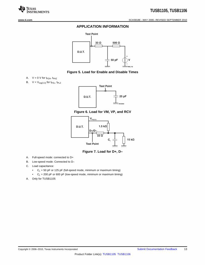
APPLICATION INFORMATION
Figure 5. Load for Enable and Disable Times
A. V = 0 V for tPZH, tPHZ
B. V = Vreg(3.3) for tPZL, tPLZ
Figure 6. Load for VM, VP, and RCV
Figure 7. Load for D+, D–
A. Full-speed mode: connected to D+
B. Low-speed mode: Connected to D–
C. Load capacitance:
• CL = 50 pF or 125 pF (full-speed mode, minimum or maximum timing)
• CL = 200 pF or 600 pF (low-speed mode, minimum or maximum timing)
A. Only for TUSB1105
Copyright © 2006–2010, Texas Instruments Incorporated Submit Documentation Feedback 13
Product Folder Link(s): TUSB1105 TUSB1106
Vpu(3.3)
SPEED
SOFTCON
RCV
VPO/VO
VP
VM
1.65 V to 3.6 V
System ASIC
D–
D+
1.5 kW
VBUS
VCC(5.0)
OE
Vreg(3.3)
SUSPND
MODE(A)
VMO/FSE0
VCC(I/O)
0.1 µF
3.3 V
VCC
33 W
33 W
0.1 µF
0.1 µF
TUSB1105/1106
GND
GND
GND
GND
GND
TUSB1105, TUSB1106
SCAS818E –MAY 2006–REVISED SEPTEMBER 2010 www.ti.com
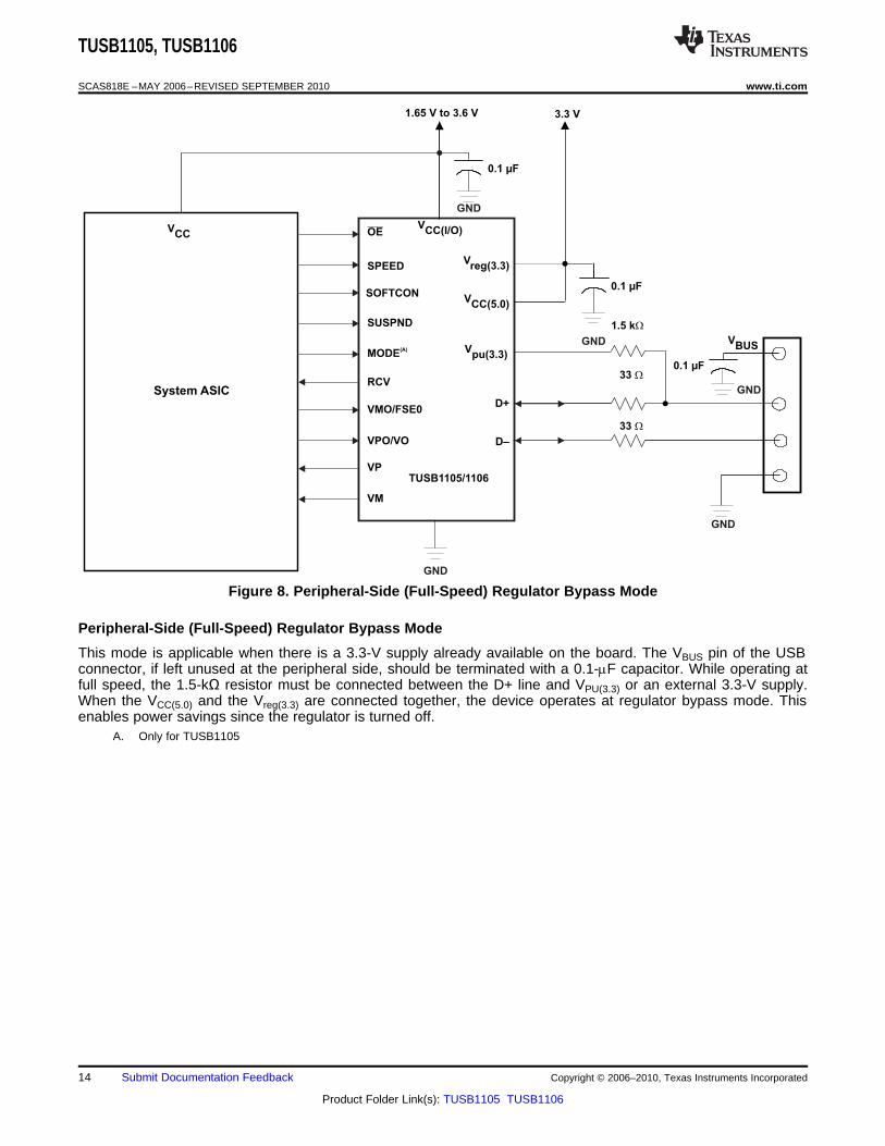
Figure 8. Peripheral-Side (Full-Speed) Regulator Bypass Mode
Peripheral-Side (Full-Speed) Regulator Bypass Mode
This mode is applicable when there is a 3.3-V supply already available on the board. The VBUS pin of the USBconnector, if left unused at the peripheral side, should be terminated with a 0.1-mF capacitor. While operating atfull speed, the 1.5-kΩ resistor must be connected between the D+ line and VPU(3.3) or an external 3.3-V supply.When the VCC(5.0) and the Vreg(3.3) are connected together, the device operates at regulator bypass mode. Thisenables power savings since the regulator is turned off.
A. Only for TUSB1105
14 Submit Documentation Feedback Copyright © 2006–2010, Texas Instruments Incorporated
Product Folder Link(s): TUSB1105 TUSB1106
Vpu(3.3)
SPEED
SOFTCON
RCV
VPO/VO
VP
VM
1.65 V to 3.6 V
System ASIC
D–
D+
1.5 kW VBUS
VCC(5.0)
OE
Vreg(3.3)
SUSPND
MODE(A)
VMO/FSE0
VCC(I/O)
0.1 µF
3.3 V
VCC
33 W
33 W
0.1 µF
0.1 µF
TUSB1105/1106
GND
GND
GND
GND
GND
TUSB1105, TUSB1106
www.ti.com SCAS818E –MAY 2006–REVISED SEPTEMBER 2010
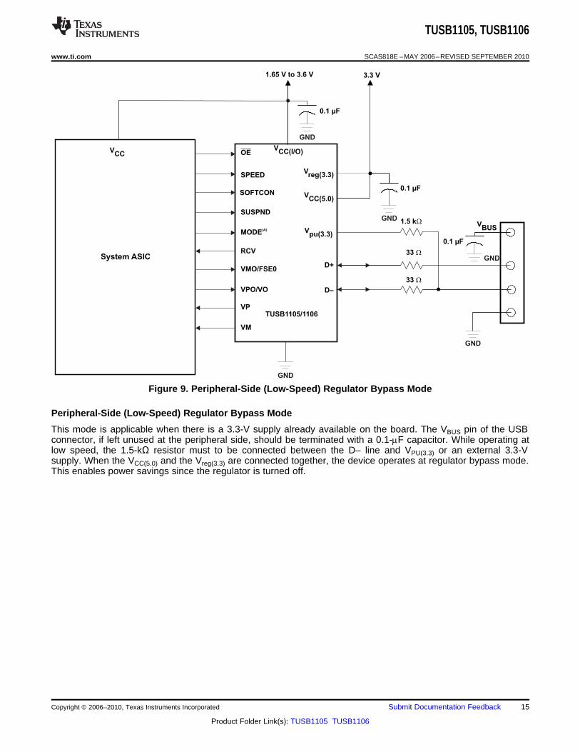
Figure 9. Peripheral-Side (Low-Speed) Regulator Bypass Mode
Peripheral-Side (Low-Speed) Regulator Bypass Mode
This mode is applicable when there is a 3.3-V supply already available on the board. The VBUS pin of the USBconnector, if left unused at the peripheral side, should be terminated with a 0.1-mF capacitor. While operating atlow speed, the 1.5-kΩ resistor must to be connected between the D– line and VPU(3.3) or an external 3.3-Vsupply. When the VCC(5.0) and the Vreg(3.3) are connected together, the device operates at regulator bypass mode.This enables power savings since the regulator is turned off.
Copyright © 2006–2010, Texas Instruments Incorporated Submit Documentation Feedback 15
Product Folder Link(s): TUSB1105 TUSB1106
V(3.3)PU
SPEED
SOFTCON
RCV
VPO/VO
VP
VM
1.65 V to 3.6 V
System ASIC
D–
D+
1.5 kW
VBUS
VCC(5.0)
OE
Vreg(3.3)
SUSPND
MODE(A)
VMO/FSE0
VCC(I/O)
0.1 µF
0.1 µF
0.1 µF
VCC
33 W
33 W
TUSB1105/1106
GND
GND
GND
GND
GND
TUSB1105, TUSB1106
SCAS818E –MAY 2006–REVISED SEPTEMBER 2010 www.ti.com
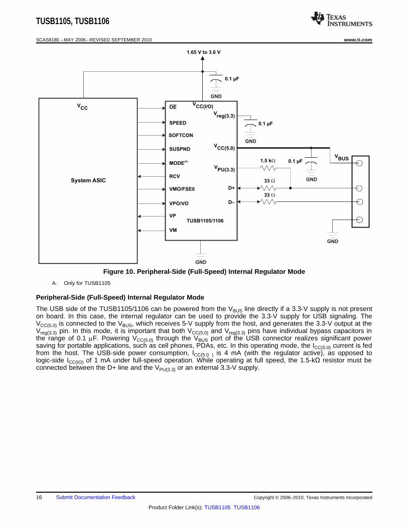
Figure 10. Peripheral-Side (Full-Speed) Internal Regulator Mode
A. Only for TUSB1105
Peripheral-Side (Full-Speed) Internal Regulator Mode
The USB side of the TUSB1105/1106 can be powered from the VBUS line directly if a 3.3-V supply is not presenton board. In this case, the internal regulator can be used to provide the 3.3-V supply for USB signaling. TheVCC(5.0) is connected to the VBUS, which receives 5-V supply from the host, and generates the 3.3-V output at theVreg(3.3) pin. In this mode, it is important that both VCC(5.0) and Vreg(3.3) pins have individual bypass capacitors inthe range of 0.1 mF. Powering VCC(5.0) through the VBUS port of the USB connector realizes significant powersaving for portable applications, such as cell phones, PDAs, etc. In this operating mode, the ICC(5.0) current is fedfrom the host. The USB-side power consumption, ICC(5.0 ) is 4 mA (with the regulator active), as opposed tologic-side ICC(IO) of 1 mA under full-speed operation. While operating at full speed, the 1.5-kΩ resistor must beconnected between the D+ line and the VPU(3.3) or an external 3.3-V supply.
16 Submit Documentation Feedback Copyright © 2006–2010, Texas Instruments Incorporated
Product Folder Link(s): TUSB1105 TUSB1106
V(3.3)PU
SPEED
SOFTCON
RCV
VPO/VO
VP
VM
1.65 V to 3.6 V
System ASIC
D–
D+
1.5 kWV
BUS
VCC(5.0)
OEV
reg(3.3)
SUSPND
MODE(A)
VMO/FSE0
VCC(I/O)
0.1 µF
0.1 µF
0.1 µF
VCC
33 W
33 W
TUSB1105/1106
GND
GND
GND
GND
GND
TUSB1105, TUSB1106
www.ti.com SCAS818E –MAY 2006–REVISED SEPTEMBER 2010
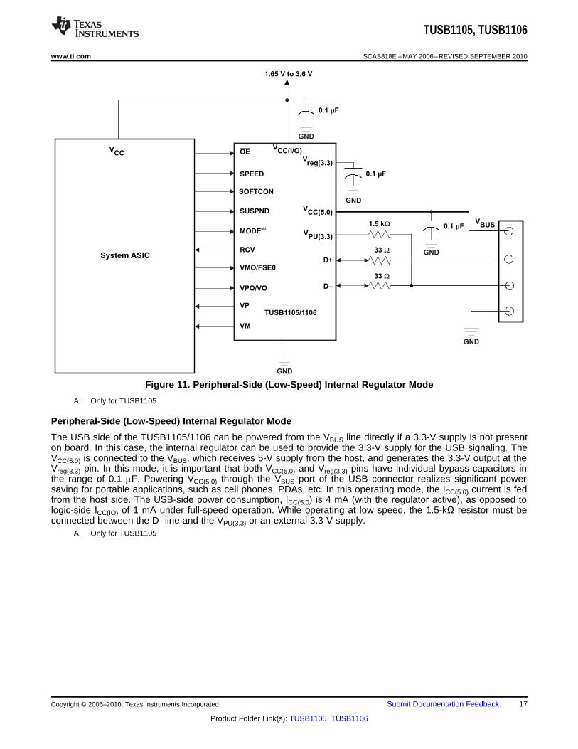
Figure 11. Peripheral-Side (Low-Speed) Internal Regulator Mode
A. Only for TUSB1105
Peripheral-Side (Low-Speed) Internal Regulator Mode
The USB side of the TUSB1105/1106 can be powered from the VBUS line directly if a 3.3-V supply is not presenton board. In this case, the internal regulator can be used to provide the 3.3-V supply for the USB signaling. TheVCC(5.0) is connected to the VBUS, which receives 5-V supply from the host, and generates the 3.3-V output at theVreg(3.3) pin. In this mode, it is important that both VCC(5.0) and Vreg(3.3) pins have individual bypass capacitors inthe range of 0.1 mF. Powering VCC(5.0) through the VBUS port of the USB connector realizes significant powersaving for portable applications, such as cell phones, PDAs, etc. In this operating mode, the ICC(5.0) current is fedfrom the host side. The USB-side power consumption, ICC(5.0) is 4 mA (with the regulator active), as opposed tologic-side ICC(IO) of 1 mA under full-speed operation. While operating at low speed, the 1.5-kΩ resistor must beconnected between the D- line and the VPU(3.3) or an external 3.3-V supply.
A. Only for TUSB1105
Copyright © 2006–2010, Texas Instruments Incorporated Submit Documentation Feedback 17
Product Folder Link(s): TUSB1105 TUSB1106
Vpu(3.3)
VCC(5.0)
Vreg(3.3)
1.65 V to 3.6 V
System ASIC
15 kW
VBUS
5 V 5 V
D–
D+
SPEED
SOFTCON
RCV
VPO/VO
VP
VM
OE
SUSPND
MODE(A)
VMO/FSE0
VCC(I/O)
0.1 µF
VCC
33 W
33 W
0.1 µF
0.1 µF
15 kW
TUSB1105/1106
GND
GND
GND
GNDGND
GND
GND
TUSB1105, TUSB1106
SCAS818E –MAY 2006–REVISED SEPTEMBER 2010 www.ti.com
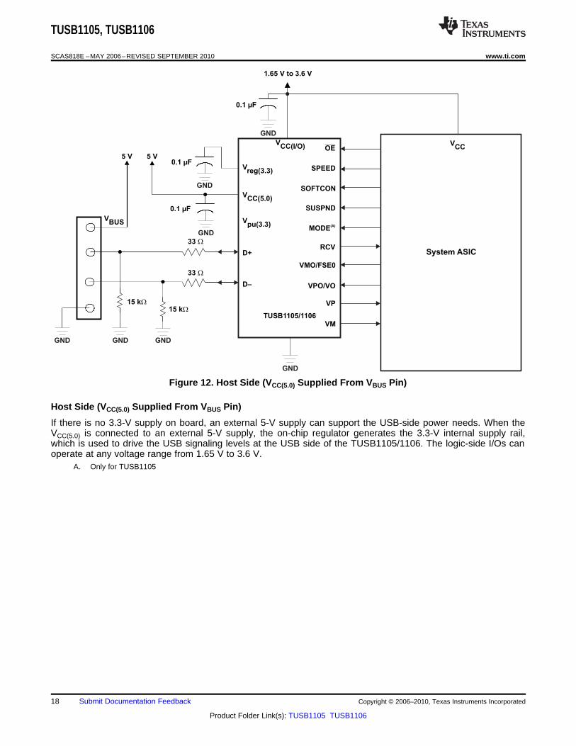
Figure 12. Host Side (VCC(5.0) Supplied From VBUS Pin)
Host Side (VCC(5.0) Supplied From VBUS Pin)
If there is no 3.3-V supply on board, an external 5-V supply can support the USB-side power needs. When theVCC(5.0) is connected to an external 5-V supply, the on-chip regulator generates the 3.3-V internal supply rail,which is used to drive the USB signaling levels at the USB side of the TUSB1105/1106. The logic-side I/Os canoperate at any voltage range from 1.65 V to 3.6 V.
A. Only for TUSB1105
18 Submit Documentation Feedback Copyright © 2006–2010, Texas Instruments Incorporated
Product Folder Link(s): TUSB1105 TUSB1106
Vpu(3.3)
VCC(5.0)
Vreg(3.3)
1.65 V to 3.6 V
System ASIC
15 kW
VBUS
D–
D+
SPEED
SOFTCON
RCV
VPO/VO
VP
VM
OE
SUSPND
MODE(A)
VMO/FSE0
VCC(I/O)
0.1 µF
VCC
33 W
33 W
0.1 µF
15 kW
3.3 V
5 V
TUSB1105/1106
GND
GND
GND GND GND
GND
TUSB1105, TUSB1106
www.ti.com SCAS818E –MAY 2006–REVISED SEPTEMBER 2010
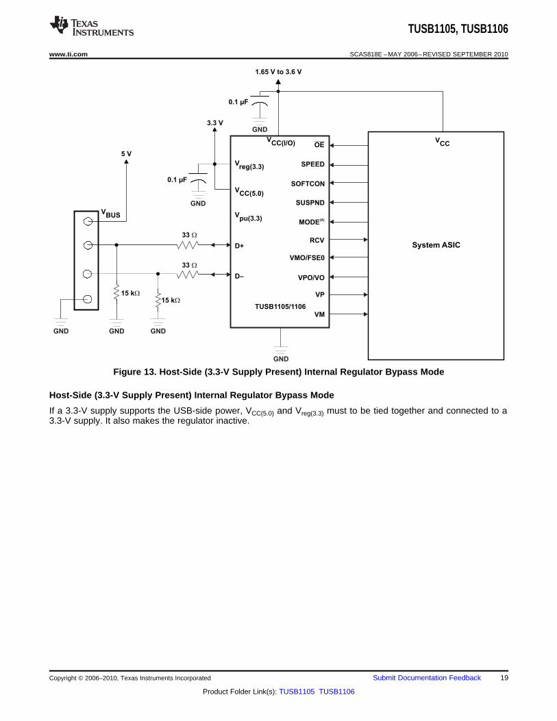
Figure 13. Host-Side (3.3-V Supply Present) Internal Regulator Bypass Mode
Host-Side (3.3-V Supply Present) Internal Regulator Bypass Mode
If a 3.3-V supply supports the USB-side power, VCC(5.0) and Vreg(3.3) must to be tied together and connected to a3.3-V supply. It also makes the regulator inactive.
Copyright © 2006–2010, Texas Instruments Incorporated Submit Documentation Feedback 19
Product Folder Link(s): TUSB1105 TUSB1106
PACKAGE OPTION ADDENDUM
www.ti.com 11-Aug-2017
Addendum-Page 1
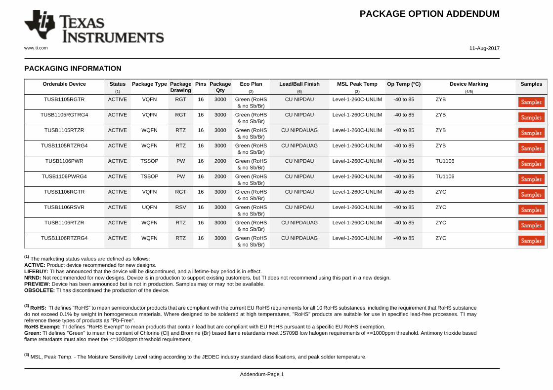
PACKAGING INFORMATION
Orderable Device Status(1)
Package Type PackageDrawing
Pins PackageQty
Eco Plan(2)
Lead/Ball Finish(6)
MSL Peak Temp(3)
Op Temp (°C) Device Marking(4/5)
Samples
TUSB1105RGTR ACTIVE VQFN RGT 16 3000 Green (RoHS& no Sb/Br)
CU NIPDAU Level-1-260C-UNLIM -40 to 85 ZYB
TUSB1105RGTRG4 ACTIVE VQFN RGT 16 3000 Green (RoHS& no Sb/Br)
CU NIPDAU Level-1-260C-UNLIM -40 to 85 ZYB
TUSB1105RTZR ACTIVE WQFN RTZ 16 3000 Green (RoHS& no Sb/Br)
CU NIPDAUAG Level-1-260C-UNLIM -40 to 85 ZYB
TUSB1105RTZRG4 ACTIVE WQFN RTZ 16 3000 Green (RoHS& no Sb/Br)
CU NIPDAUAG Level-1-260C-UNLIM -40 to 85 ZYB
TUSB1106PWR ACTIVE TSSOP PW 16 2000 Green (RoHS& no Sb/Br)
CU NIPDAU Level-1-260C-UNLIM -40 to 85 TU1106
TUSB1106PWRG4 ACTIVE TSSOP PW 16 2000 Green (RoHS& no Sb/Br)
CU NIPDAU Level-1-260C-UNLIM -40 to 85 TU1106
TUSB1106RGTR ACTIVE VQFN RGT 16 3000 Green (RoHS& no Sb/Br)
CU NIPDAU Level-1-260C-UNLIM -40 to 85 ZYC
TUSB1106RSVR ACTIVE UQFN RSV 16 3000 Green (RoHS& no Sb/Br)
CU NIPDAU Level-1-260C-UNLIM -40 to 85 ZYC
TUSB1106RTZR ACTIVE WQFN RTZ 16 3000 Green (RoHS& no Sb/Br)
CU NIPDAUAG Level-1-260C-UNLIM -40 to 85 ZYC
TUSB1106RTZRG4 ACTIVE WQFN RTZ 16 3000 Green (RoHS& no Sb/Br)
CU NIPDAUAG Level-1-260C-UNLIM -40 to 85 ZYC
(1) The marketing status values are defined as follows:ACTIVE: Product device recommended for new designs.LIFEBUY: TI has announced that the device will be discontinued, and a lifetime-buy period is in effect.NRND: Not recommended for new designs. Device is in production to support existing customers, but TI does not recommend using this part in a new design.PREVIEW: Device has been announced but is not in production. Samples may or may not be available.OBSOLETE: TI has discontinued the production of the device.
(2) RoHS: TI defines "RoHS" to mean semiconductor products that are compliant with the current EU RoHS requirements for all 10 RoHS substances, including the requirement that RoHS substancedo not exceed 0.1% by weight in homogeneous materials. Where designed to be soldered at high temperatures, "RoHS" products are suitable for use in specified lead-free processes. TI mayreference these types of products as "Pb-Free".RoHS Exempt: TI defines "RoHS Exempt" to mean products that contain lead but are compliant with EU RoHS pursuant to a specific EU RoHS exemption.Green: TI defines "Green" to mean the content of Chlorine (Cl) and Bromine (Br) based flame retardants meet JS709B low halogen requirements of <=1000ppm threshold. Antimony trioxide basedflame retardants must also meet the <=1000ppm threshold requirement.
(3) MSL, Peak Temp. - The Moisture Sensitivity Level rating according to the JEDEC industry standard classifications, and peak solder temperature.
PACKAGE OPTION ADDENDUM
www.ti.com 11-Aug-2017
Addendum-Page 2
(4) There may be additional marking, which relates to the logo, the lot trace code information, or the environmental category on the device.
(5) Multiple Device Markings will be inside parentheses. Only one Device Marking contained in parentheses and separated by a "~" will appear on a device. If a line is indented then it is a continuationof the previous line and the two combined represent the entire Device Marking for that device.
(6) Lead/Ball Finish - Orderable Devices may have multiple material finish options. Finish options are separated by a vertical ruled line. Lead/Ball Finish values may wrap to two lines if the finishvalue exceeds the maximum column width.
Important Information and Disclaimer:The information provided on this page represents TI's knowledge and belief as of the date that it is provided. TI bases its knowledge and belief on informationprovided by third parties, and makes no representation or warranty as to the accuracy of such information. Efforts are underway to better integrate information from third parties. TI has taken andcontinues to take reasonable steps to provide representative and accurate information but may not have conducted destructive testing or chemical analysis on incoming materials and chemicals.TI and TI suppliers consider certain information to be proprietary, and thus CAS numbers and other limited information may not be available for release.
In no event shall TI's liability arising out of such information exceed the total purchase price of the TI part(s) at issue in this document sold by TI to Customer on an annual basis.
OTHER QUALIFIED VERSIONS OF TUSB1106 :
• Automotive: TUSB1106-Q1
NOTE: Qualified Version Definitions:
• Automotive - Q100 devices qualified for high-reliability automotive applications targeting zero defects
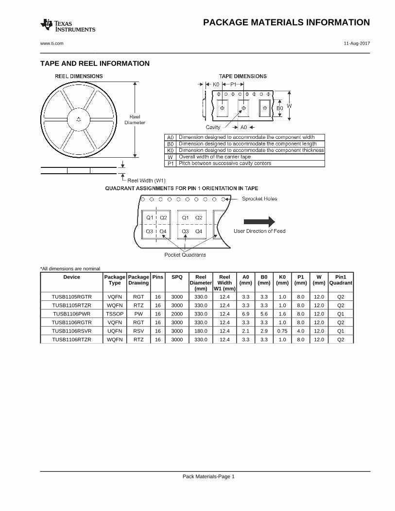
TAPE AND REEL INFORMATION
*All dimensions are nominal
Device PackageType
PackageDrawing
Pins SPQ ReelDiameter
(mm)
ReelWidth
W1 (mm)
A0(mm)
B0(mm)
K0(mm)
P1(mm)
W(mm)
Pin1Quadrant
TUSB1105RGTR VQFN RGT 16 3000 330.0 12.4 3.3 3.3 1.0 8.0 12.0 Q2
TUSB1105RTZR WQFN RTZ 16 3000 330.0 12.4 3.3 3.3 1.0 8.0 12.0 Q2
TUSB1106PWR TSSOP PW 16 2000 330.0 12.4 6.9 5.6 1.6 8.0 12.0 Q1
TUSB1106RGTR VQFN RGT 16 3000 330.0 12.4 3.3 3.3 1.0 8.0 12.0 Q2
TUSB1106RSVR UQFN RSV 16 3000 180.0 12.4 2.1 2.9 0.75 4.0 12.0 Q1
TUSB1106RTZR WQFN RTZ 16 3000 330.0 12.4 3.3 3.3 1.0 8.0 12.0 Q2
PACKAGE MATERIALS INFORMATION
www.ti.com 11-Aug-2017
Pack Materials-Page 1
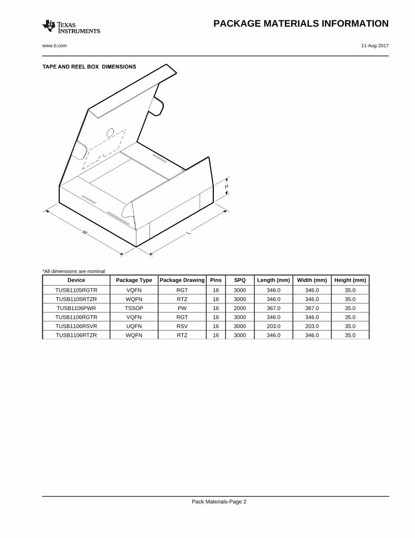
*All dimensions are nominal
Device Package Type Package Drawing Pins SPQ Length (mm) Width (mm) Height (mm)
TUSB1105RGTR VQFN RGT 16 3000 346.0 346.0 35.0
TUSB1105RTZR WQFN RTZ 16 3000 346.0 346.0 35.0
TUSB1106PWR TSSOP PW 16 2000 367.0 367.0 35.0
TUSB1106RGTR VQFN RGT 16 3000 346.0 346.0 35.0
TUSB1106RSVR UQFN RSV 16 3000 203.0 203.0 35.0
TUSB1106RTZR WQFN RTZ 16 3000 346.0 346.0 35.0
PACKAGE MATERIALS INFORMATION
www.ti.com 11-Aug-2017
Pack Materials-Page 2
www.ti.com
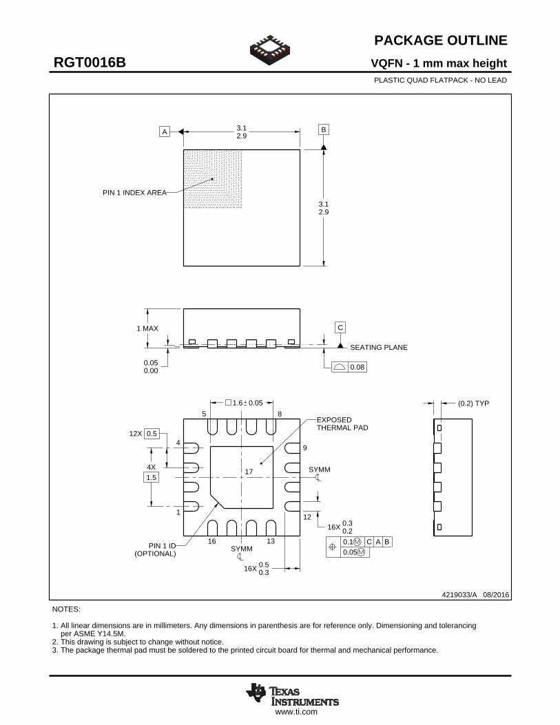
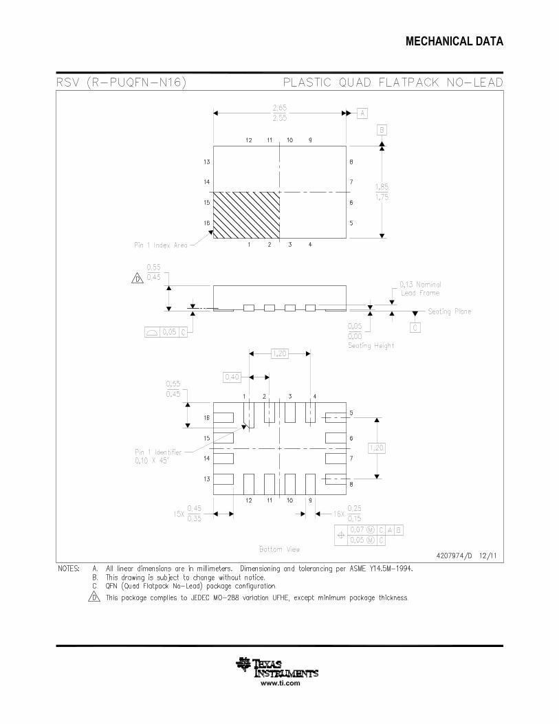
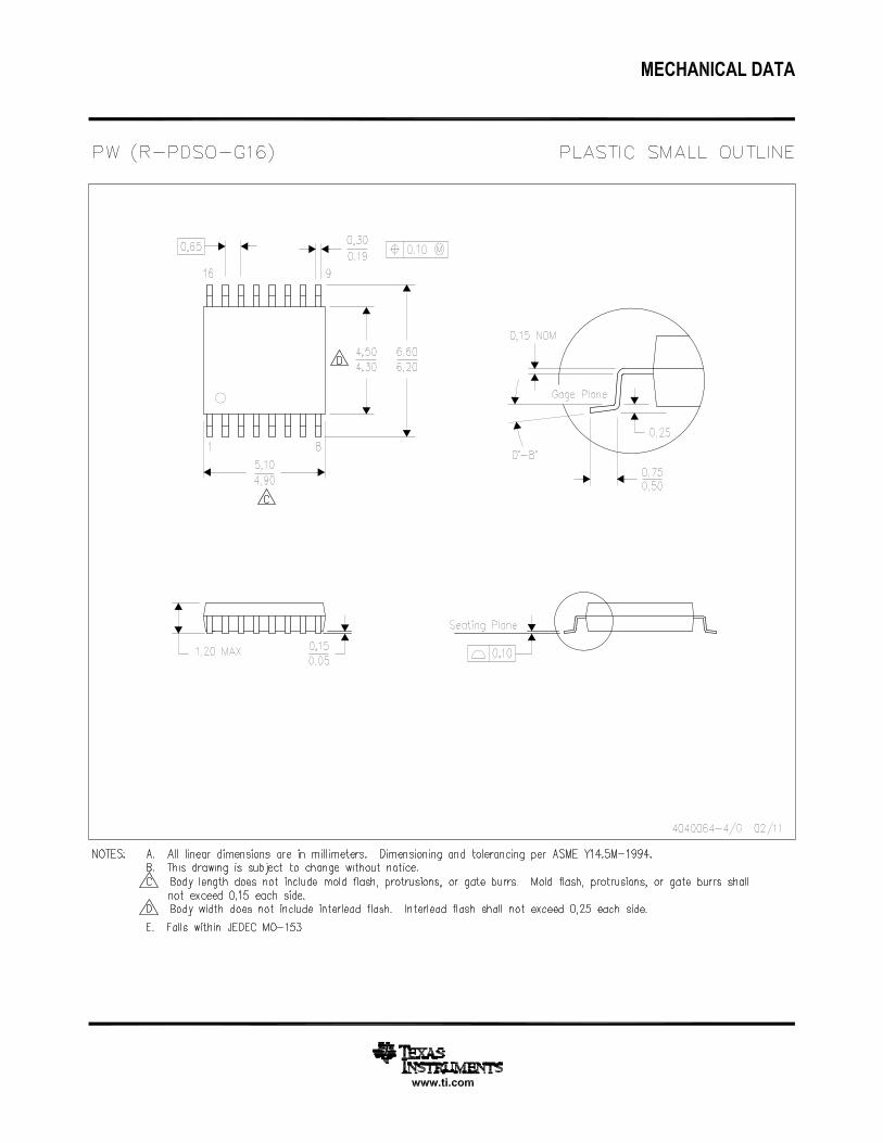
PACKAGE OUTLINE
C
16X 0.30.2
1.6 0.05
16X 0.50.3
1 MAX
(0.2) TYP
0.050.00
12X 0.5
4X1.5
A 3.12.9
B
3.12.9
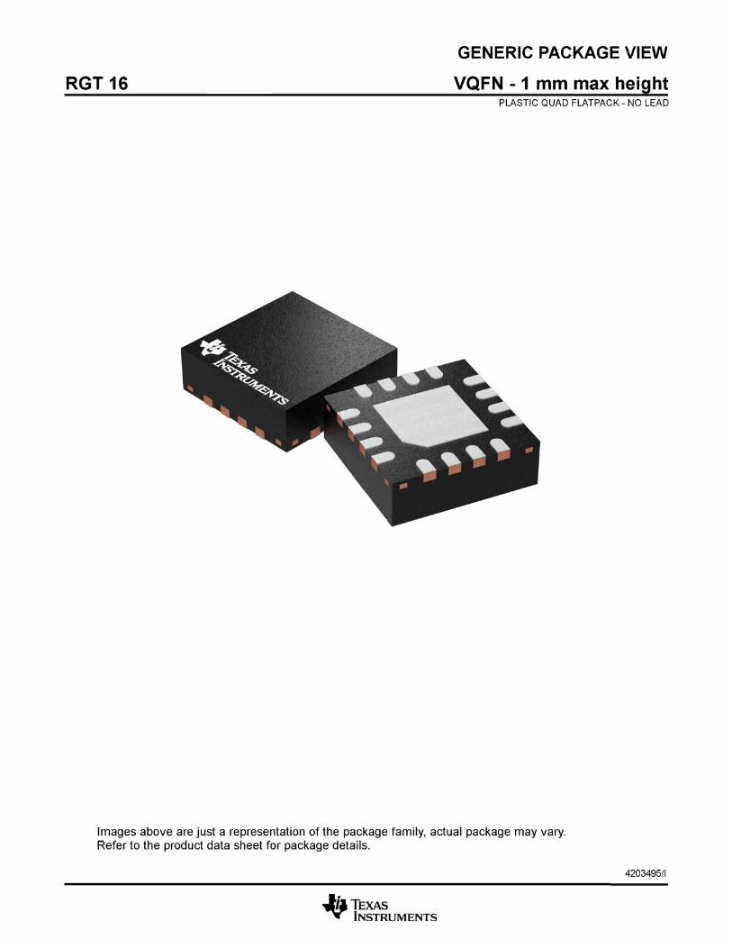
VQFN - 1 mm max heightRGT0016BPLASTIC QUAD FLATPACK - NO LEAD
4219033/A 08/2016
PIN 1 INDEX AREA
0.08
SEATING PLANE
1
49
12
5 8
16 13
(OPTIONAL)PIN 1 ID 0.1 C A B
0.05
EXPOSEDTHERMAL PAD
17 SYMM
SYMM
NOTES: 1. All linear dimensions are in millimeters. Any dimensions in parenthesis are for reference only. Dimensioning and tolerancing per ASME Y14.5M. 2. This drawing is subject to change without notice. 3. The package thermal pad must be soldered to the printed circuit board for thermal and mechanical performance.
SCALE 3.600
www.ti.com
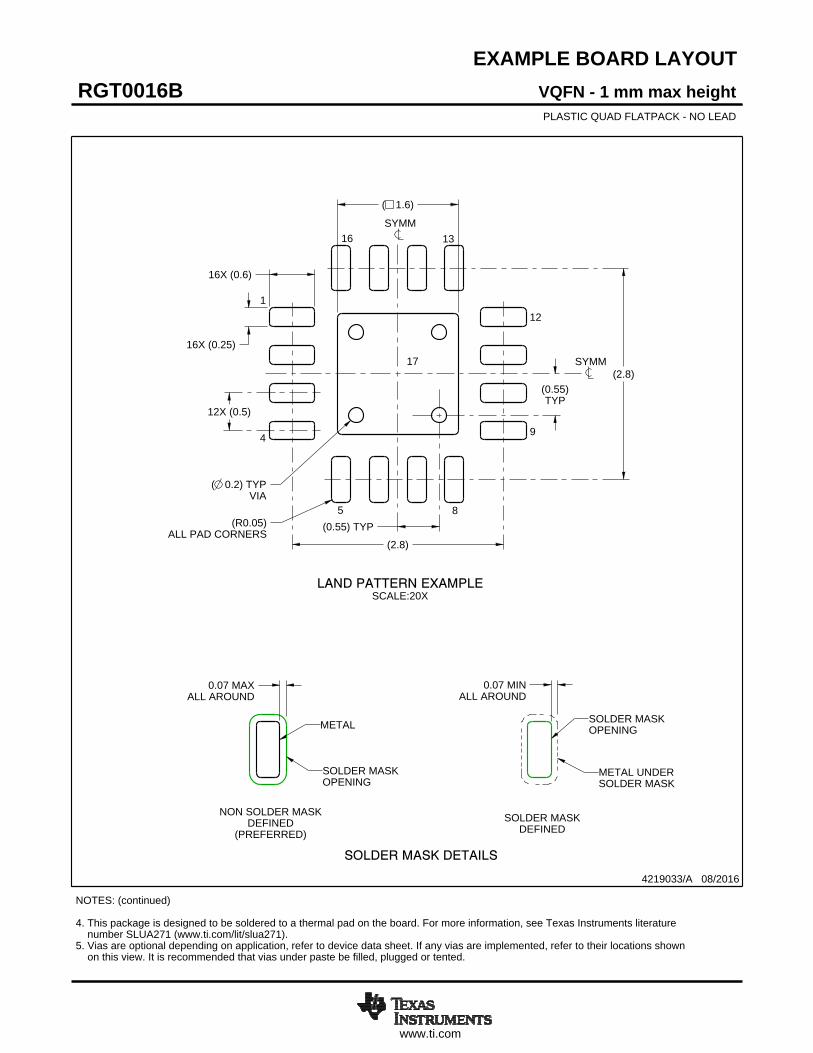
EXAMPLE BOARD LAYOUT
0.07 MINALL AROUND
0.07 MAXALL AROUND
16X (0.25)
16X (0.6)
( 0.2) TYPVIA
12X (0.5)
(2.8)
(2.8)
(0.55)TYP
( 1.6)
(R0.05)ALL PAD CORNERS
(0.55) TYP
VQFN - 1 mm max heightRGT0016BPLASTIC QUAD FLATPACK - NO LEAD
4219033/A 08/2016
SYMM
1
4
5 8
9
12
1316
SYMM
LAND PATTERN EXAMPLESCALE:20X
17
NOTES: (continued) 4. This package is designed to be soldered to a thermal pad on the board. For more information, see Texas Instruments literature number SLUA271 (www.ti.com/lit/slua271).5. Vias are optional depending on application, refer to device data sheet. If any vias are implemented, refer to their locations shown on this view. It is recommended that vias under paste be filled, plugged or tented.
SOLDER MASKOPENING
METAL UNDERSOLDER MASK
SOLDER MASKDEFINED
METAL
SOLDER MASKOPENING
SOLDER MASK DETAILS
NON SOLDER MASKDEFINED
(PREFERRED)
www.ti.com
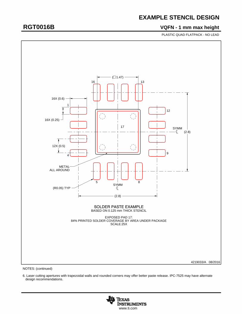
EXAMPLE STENCIL DESIGN
16X (0.6)
16X (0.25)
12X (0.5)
(2.8)
(2.8)
( 1.47)
(R0.05) TYP
VQFN - 1 mm max heightRGT0016BPLASTIC QUAD FLATPACK - NO LEAD
4219033/A 08/2016
NOTES: (continued) 6. Laser cutting apertures with trapezoidal walls and rounded corners may offer better paste release. IPC-7525 may have alternate design recommendations.
SYMM
ALL AROUNDMETAL
SOLDER PASTE EXAMPLEBASED ON 0.125 mm THICK STENCIL
EXPOSED PAD 17:
84% PRINTED SOLDER COVERAGE BY AREA UNDER PACKAGESCALE:25X
SYMM
1
4
5 8
9
12
1316
17
IMPORTANT NOTICE
Texas Instruments Incorporated (TI) reserves the right to make corrections, enhancements, improvements and other changes to itssemiconductor products and services per JESD46, latest issue, and to discontinue any product or service per JESD48, latest issue. Buyersshould obtain the latest relevant information before placing orders and should verify that such information is current and complete.TI’s published terms of sale for semiconductor products (http://www.ti.com/sc/docs/stdterms.htm) apply to the sale of packaged integratedcircuit products that TI has qualified and released to market. Additional terms may apply to the use or sale of other types of TI products andservices.Reproduction of significant portions of TI information in TI data sheets is permissible only if reproduction is without alteration and isaccompanied by all associated warranties, conditions, limitations, and notices. TI is not responsible or liable for such reproduceddocumentation. Information of third parties may be subject to additional restrictions. Resale of TI products or services with statementsdifferent from or beyond the parameters stated by TI for that product or service voids all express and any implied warranties for theassociated TI product or service and is an unfair and deceptive business practice. TI is not responsible or liable for any such statements.Buyers and others who are developing systems that incorporate TI products (collectively, “Designers”) understand and agree that Designersremain responsible for using their independent analysis, evaluation and judgment in designing their applications and that Designers havefull and exclusive responsibility to assure the safety of Designers' applications and compliance of their applications (and of all TI productsused in or for Designers’ applications) with all applicable regulations, laws and other applicable requirements. Designer represents that, withrespect to their applications, Designer has all the necessary expertise to create and implement safeguards that (1) anticipate dangerousconsequences of failures, (2) monitor failures and their consequences, and (3) lessen the likelihood of failures that might cause harm andtake appropriate actions. Designer agrees that prior to using or distributing any applications that include TI products, Designer willthoroughly test such applications and the functionality of such TI products as used in such applications.TI’s provision of technical, application or other design advice, quality characterization, reliability data or other services or information,including, but not limited to, reference designs and materials relating to evaluation modules, (collectively, “TI Resources”) are intended toassist designers who are developing applications that incorporate TI products; by downloading, accessing or using TI Resources in anyway, Designer (individually or, if Designer is acting on behalf of a company, Designer’s company) agrees to use any particular TI Resourcesolely for this purpose and subject to the terms of this Notice.TI’s provision of TI Resources does not expand or otherwise alter TI’s applicable published warranties or warranty disclaimers for TIproducts, and no additional obligations or liabilities arise from TI providing such TI Resources. TI reserves the right to make corrections,enhancements, improvements and other changes to its TI Resources. TI has not conducted any testing other than that specificallydescribed in the published documentation for a particular TI Resource.Designer is authorized to use, copy and modify any individual TI Resource only in connection with the development of applications thatinclude the TI product(s) identified in such TI Resource. NO OTHER LICENSE, EXPRESS OR IMPLIED, BY ESTOPPEL OR OTHERWISETO ANY OTHER TI INTELLECTUAL PROPERTY RIGHT, AND NO LICENSE TO ANY TECHNOLOGY OR INTELLECTUAL PROPERTYRIGHT OF TI OR ANY THIRD PARTY IS GRANTED HEREIN, including but not limited to any patent right, copyright, mask work right, orother intellectual property right relating to any combination, machine, or process in which TI products or services are used. Informationregarding or referencing third-party products or services does not constitute a license to use such products or services, or a warranty orendorsement thereof. Use of TI Resources may require a license from a third party under the patents or other intellectual property of thethird party, or a license from TI under the patents or other intellectual property of TI.TI RESOURCES ARE PROVIDED “AS IS” AND WITH ALL FAULTS. TI DISCLAIMS ALL OTHER WARRANTIES ORREPRESENTATIONS, EXPRESS OR IMPLIED, REGARDING RESOURCES OR USE THEREOF, INCLUDING BUT NOT LIMITED TOACCURACY OR COMPLETENESS, TITLE, ANY EPIDEMIC FAILURE WARRANTY AND ANY IMPLIED WARRANTIES OFMERCHANTABILITY, FITNESS FOR A PARTICULAR PURPOSE, AND NON-INFRINGEMENT OF ANY THIRD PARTY INTELLECTUALPROPERTY RIGHTS. TI SHALL NOT BE LIABLE FOR AND SHALL NOT DEFEND OR INDEMNIFY DESIGNER AGAINST ANY CLAIM,INCLUDING BUT NOT LIMITED TO ANY INFRINGEMENT CLAIM THAT RELATES TO OR IS BASED ON ANY COMBINATION OFPRODUCTS EVEN IF DESCRIBED IN TI RESOURCES OR OTHERWISE. IN NO EVENT SHALL TI BE LIABLE FOR ANY ACTUAL,DIRECT, SPECIAL, COLLATERAL, INDIRECT, PUNITIVE, INCIDENTAL, CONSEQUENTIAL OR EXEMPLARY DAMAGES INCONNECTION WITH OR ARISING OUT OF TI RESOURCES OR USE THEREOF, AND REGARDLESS OF WHETHER TI HAS BEENADVISED OF THE POSSIBILITY OF SUCH DAMAGES.Unless TI has explicitly designated an individual product as meeting the requirements of a particular industry standard (e.g., ISO/TS 16949and ISO 26262), TI is not responsible for any failure to meet such industry standard requirements.Where TI specifically promotes products as facilitating functional safety or as compliant with industry functional safety standards, suchproducts are intended to help enable customers to design and create their own applications that meet applicable functional safety standardsand requirements. Using products in an application does not by itself establish any safety features in the application. Designers mustensure compliance with safety-related requirements and standards applicable to their applications. Designer may not use any TI products inlife-critical medical equipment unless authorized officers of the parties have executed a special contract specifically governing such use.Life-critical medical equipment is medical equipment where failure of such equipment would cause serious bodily injury or death (e.g., lifesupport, pacemakers, defibrillators, heart pumps, neurostimulators, and implantables). Such equipment includes, without limitation, allmedical devices identified by the U.S. Food and Drug Administration as Class III devices and equivalent classifications outside the U.S.TI may expressly designate certain products as completing a particular qualification (e.g., Q100, Military Grade, or Enhanced Product).Designers agree that it has the necessary expertise to select the product with the appropriate qualification designation for their applicationsand that proper product selection is at Designers’ own risk. Designers are solely responsible for compliance with all legal and regulatoryrequirements in connection with such selection.Designer will fully indemnify TI and its representatives against any damages, costs, losses, and/or liabilities arising out of Designer’s non-compliance with the terms and provisions of this Notice.
Mailing Address: Texas Instruments, Post Office Box 655303, Dallas, Texas 75265Copyright © 2017, Texas Instruments Incorporated