Embed Size (px)
Citation preview
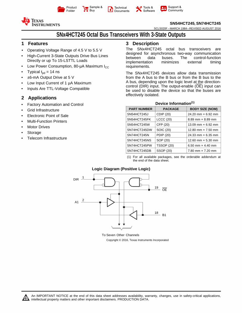
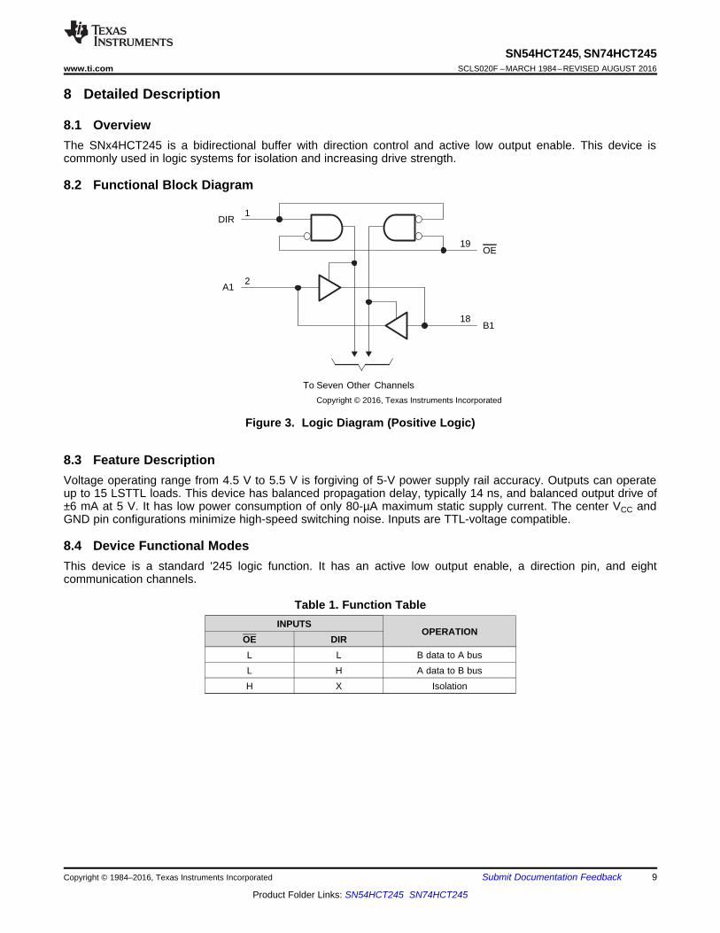
DIR
OE
A1
B1
1
2
18
19
To Seven Other Channels
Copyright © 2016, Texas Instruments Incorporated
Product
Folder
Sample &Buy
Technical
Documents
Tools &
Software
Support &Community
An IMPORTANT NOTICE at the end of this data sheet addresses availability, warranty, changes, use in safety-critical applications,intellectual property matters and other important disclaimers. PRODUCTION DATA.
SN54HCT245, SN74HCT245SCLS020F –MARCH 1984–REVISED AUGUST 2016
SNx4HCT245 Octal Bus Transceivers With 3-State Outputs
1
1 Features1• Operating Voltage Range of 4.5 V to 5.5 V• High-Current 3-State Outputs Drive Bus Lines
Directly or up To 15-LSTTL Loads• Low Power Consumption, 80-µA Maximum ICC
• Typical tpd = 14 ns• ±6-mA Output Drive at 5 V• Low Input Current of 1 µA Maximum• Inputs Are TTL-Voltage Compatible
2 Applications• Factory Automation and Control• Grid Infrastructure• Electronic Point of Sale• Multi-Function Printers• Motor Drives• Storage• Telecom Infrastructure
3 DescriptionThe SNx4HCT245 octal bus transceivers aredesigned for asynchronous two-way communicationbetween data buses. The control-functionimplementation minimizes external timingrequirements.
The SNx4HCT245 devices allow data transmissionfrom the A bus to the B bus or from the B bus to theA bus, depending upon the logic level at the direction-control (DIR) input. The output-enable (OE) input canbe used to disable the device so that the buses areeffectively isolated.
Device Information(1)
PART NUMBER PACKAGE BODY SIZE (NOM)SN54HCT245J CDIP (20) 24.20 mm × 6.92 mmSN54HCT245FK LCCC (20) 8.89 mm × 8.89 mmSN54HCT245W CFP (20) 13.09 mm × 6.92 mmSN74HCT245DW SOIC (20) 12.80 mm × 7.50 mmSN74HCT245N PDIP (20) 24.33 mm × 6.35 mmSN74HCT245NS SOP (20) 12.60 mm × 5.30 mmSN74HCT245PW TSSOP (20) 6.50 mm × 4.40 mmSN74HCT245DB SSOP (20) 7.80 mm × 7.20 mm
(1) For all available packages, see the orderable addendum atthe end of the data sheet.
Logic Diagram (Positive Logic)
2
SN54HCT245, SN74HCT245SCLS020F –MARCH 1984–REVISED AUGUST 2016 www.ti.com
Product Folder Links: SN54HCT245 SN74HCT245
Submit Documentation Feedback Copyright © 1984–2016, Texas Instruments Incorporated
Table of Contents1 Features .................................................................. 12 Applications ........................................................... 13 Description ............................................................. 14 Revision History..................................................... 25 Pin Configuration and Functions ......................... 36 Specifications......................................................... 4
6.1 Absolute Maximum Ratings ...................................... 46.2 ESD Ratings.............................................................. 46.3 Recommended Operating Conditions....................... 46.4 Thermal Information .................................................. 56.5 Electrical Characteristics........................................... 56.6 Switching Characteristics: CL = 50 pF ...................... 66.7 Switching Characteristics: CL = 150 pF .................... 76.8 Operating Characteristics.......................................... 76.9 Typical Characteristics .............................................. 7
7 Parameter Measurement Information .................. 88 Detailed Description .............................................. 9
8.1 Overview ................................................................... 98.2 Functional Block Diagram ......................................... 9
8.3 Feature Description................................................... 98.4 Device Functional Modes.......................................... 9
9 Application and Implementation ........................ 109.1 Application Information............................................ 109.2 Typical Application ................................................. 10
10 Power Supply Recommendations ..................... 1211 Layout................................................................... 12
11.1 Layout Guidelines ................................................. 1211.2 Layout Example .................................................... 12
12 Device and Documentation Support ................. 1312.1 Documentation Support ........................................ 1312.2 Related Links ........................................................ 1312.3 Receiving Notification of Documentation Updates 1312.4 Community Resource............................................ 1312.5 Trademarks ........................................................... 1312.6 Electrostatic Discharge Caution............................ 1312.7 Glossary ................................................................ 13
13 Mechanical, Packaging, and OrderableInformation ........................................................... 13
4 Revision HistoryNOTE: Page numbers for previous revisions may differ from page numbers in the current version.
Changes from Revision E (August 2003) to Revision F Page
• Deleted Ordering Information, see POA at the end of the datasheet. ................................................................................... 1• Added ESD Ratings table, Feature Description section, Device Functional Modes, Application and Implementation
section, Power Supply Recommendations section, Layout section, Device and Documentation Support section, andMechanical, Packaging, and Orderable Information section ................................................................................................. 1
• Updated values in the Thermal Information table................................................................................................................... 5
3 2 1 20 19
9 10 11 12 13
4
5
6
7
8
18
17
16
15
14
B1
B2
B3
B4
B5
A3
A4
A5
A6
A7
A2
A1
DIR
B7
B6
OE
A8
GN
D
B8
VC
C
SN54HCT245 . . . FK PACKAGE
(TOP VIEW)
1
2
3
4
5
6
7
8
9
10
20
19
18
17
16
15
14
13
12
11
DIR
A1
A2
A3
A4
A5
A6
A7
A8
GND
VCC
OE
B1
B2
B3
B4
B5
B6
B7
B8
SN54HCT245 . . . J OR W PACKAGE
SN74HCT245 . . . DB, DW, N, NS, OR PW PACKAGE
(TOP VIEW)
3
SN54HCT245, SN74HCT245www.ti.com SCLS020F –MARCH 1984–REVISED AUGUST 2016
Product Folder Links: SN54HCT245 SN74HCT245
Submit Documentation FeedbackCopyright © 1984–2016, Texas Instruments Incorporated
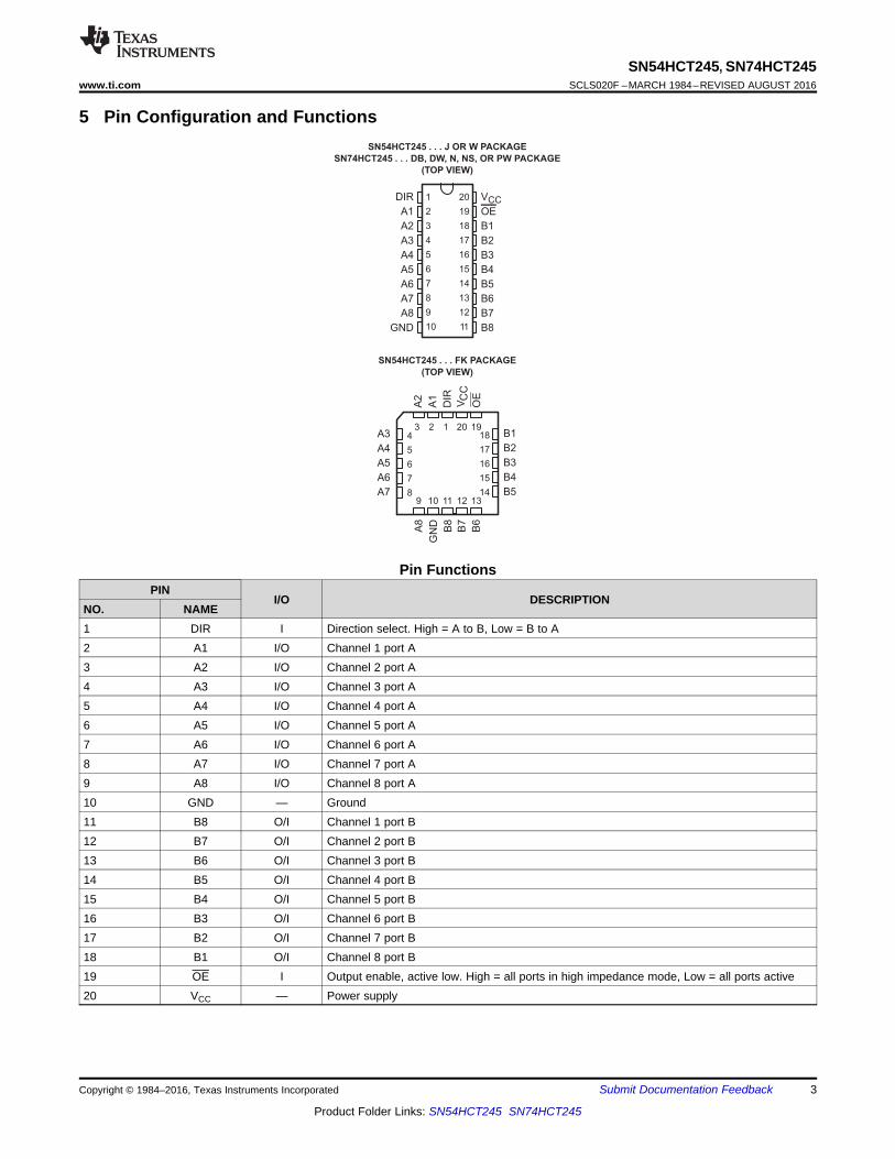
5 Pin Configuration and Functions
Pin FunctionsPIN
I/O DESCRIPTIONNO. NAME1 DIR I Direction select. High = A to B, Low = B to A2 A1 I/O Channel 1 port A3 A2 I/O Channel 2 port A4 A3 I/O Channel 3 port A5 A4 I/O Channel 4 port A6 A5 I/O Channel 5 port A7 A6 I/O Channel 6 port A8 A7 I/O Channel 7 port A9 A8 I/O Channel 8 port A10 GND — Ground11 B8 O/I Channel 1 port B12 B7 O/I Channel 2 port B13 B6 O/I Channel 3 port B14 B5 O/I Channel 4 port B15 B4 O/I Channel 5 port B16 B3 O/I Channel 6 port B17 B2 O/I Channel 7 port B18 B1 O/I Channel 8 port B19 OE I Output enable, active low. High = all ports in high impedance mode, Low = all ports active20 VCC — Power supply
4
SN54HCT245, SN74HCT245SCLS020F –MARCH 1984–REVISED AUGUST 2016 www.ti.com
Product Folder Links: SN54HCT245 SN74HCT245
Submit Documentation Feedback Copyright © 1984–2016, Texas Instruments Incorporated
(1) Stresses beyond those listed under Absolute Maximum Ratings may cause permanent damage to the device. These are stress ratingsonly, which do not imply functional operation of the device at these or any other conditions beyond those indicated under RecommendedOperating Conditions. Exposure to absolute-maximum-rated conditions for extended periods may affect device reliability.
(2) The input and output voltage ratings may be exceeded if the input and output current ratings are observed.
6 Specifications
6.1 Absolute Maximum Ratingsover operating free-air temperature range (unless otherwise noted) (1)
MIN MAX UNITVCC Supply voltage –0.5 7 VIIK Input clamp current (2) VI < 0 or VI > VCC ±20 mAIOK Output clamp current (2) VO < 0 or VO > VCC ±20 mAIO Continuous output current VO = 0 to VCC ±35 mA
Continuous current through VCC or GND ±70 mATJ Operating virtual junction temperature 150 °CTstg Storage temperature –65 150 °C
(1) JEDEC document JEP155 states that 500-V HBM allows safe manufacturing with a standard ESD control process.(2) JEDEC document JEP157 states that 250-V CDM allows safe manufacturing with a standard ESD control process.
6.2 ESD RatingsVALUE UNIT
V(ESD) Electrostatic dischargeHuman-body model (HBM), per ANSI/ESDA/JEDEC JS-001 (1) ±1500
VCharged-device model (CDM), per JEDEC specification JESD22-C101 (2) ±2000
(1) All unused inputs of the device must be held at VCC or GND to ensure proper device operation. See the TI application report,Implications of Slow or Floating CMOS Inputs (SCBA004).
6.3 Recommended Operating Conditionsover operating free-air temperature range (unless otherwise noted) (1)
MIN NOM MAX UNITVCC Supply voltage 4.5 5 5.5 VVIH High-level input voltage VCC = 4.5 V to 5.5 V 2 VVIL Low-level input voltage VCC = 4.5 V to 5.5 V 0.8 VVI Input voltage 0 VCC VVO Output voltage 0 VCC VΔt/Δv Input transition rise and fall time 500 ns
TA Operating free-air temperatureSN54HCT245 –55 125
°CSN74HCT245 –40 85
5
SN54HCT245, SN74HCT245www.ti.com SCLS020F –MARCH 1984–REVISED AUGUST 2016
Product Folder Links: SN54HCT245 SN74HCT245
Submit Documentation FeedbackCopyright © 1984–2016, Texas Instruments Incorporated
(1) For more information about traditional and new thermal metrics, see the Semiconductor and IC Package Thermal Metrics applicationreport.
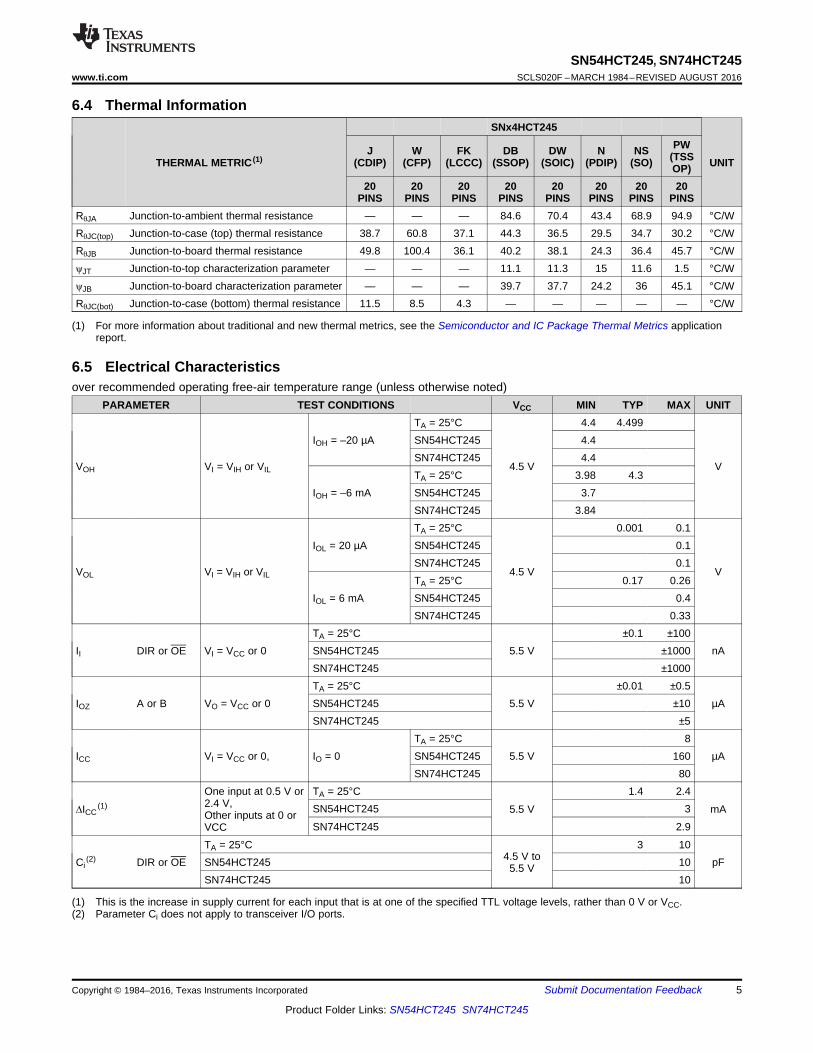
6.4 Thermal Information
THERMAL METRIC (1)
SNx4HCT245
UNITJ
(CDIP)W
(CFP)FK
(LCCC)DB
(SSOP)DW
(SOIC)N
(PDIP)NS
(SO)PW
(TSSOP)
20PINS
20PINS
20PINS
20PINS
20PINS
20PINS
20PINS
20PINS
RθJA Junction-to-ambient thermal resistance — — — 84.6 70.4 43.4 68.9 94.9 °C/WRθJC(top) Junction-to-case (top) thermal resistance 38.7 60.8 37.1 44.3 36.5 29.5 34.7 30.2 °C/WRθJB Junction-to-board thermal resistance 49.8 100.4 36.1 40.2 38.1 24.3 36.4 45.7 °C/WψJT Junction-to-top characterization parameter — — — 11.1 11.3 15 11.6 1.5 °C/WψJB Junction-to-board characterization parameter — — — 39.7 37.7 24.2 36 45.1 °C/WRθJC(bot) Junction-to-case (bottom) thermal resistance 11.5 8.5 4.3 — — — — — °C/W
(1) This is the increase in supply current for each input that is at one of the specified TTL voltage levels, rather than 0 V or VCC.(2) Parameter Ci does not apply to transceiver I/O ports.
6.5 Electrical Characteristicsover recommended operating free-air temperature range (unless otherwise noted)
PARAMETER TEST CONDITIONS VCC MIN TYP MAX UNIT
VOH VI = VIH or VIL
IOH = –20 µATA = 25°C
4.5 V
4.4 4.499
V
SN54HCT245 4.4SN74HCT245 4.4
IOH = –6 mATA = 25°C 3.98 4.3SN54HCT245 3.7SN74HCT245 3.84
VOL VI = VIH or VIL
IOL = 20 µATA = 25°C
4.5 V
0.001 0.1
V
SN54HCT245 0.1SN74HCT245 0.1
IOL = 6 mATA = 25°C 0.17 0.26SN54HCT245 0.4SN74HCT245 0.33
II DIR or OE VI = VCC or 0TA = 25°C
5.5 V±0.1 ±100
nASN54HCT245 ±1000SN74HCT245 ±1000
IOZ A or B VO = VCC or 0TA = 25°C
5.5 V±0.01 ±0.5
µASN54HCT245 ±10SN74HCT245 ±5
ICC VI = VCC or 0, IO = 0TA = 25°C
5.5 V8
µASN54HCT245 160SN74HCT245 80
∆ICC(1)
One input at 0.5 V or2.4 V,Other inputs at 0 orVCC
TA = 25°C
5.5 V
1.4 2.4
mASN54HCT245 3
SN74HCT245 2.9
Ci(2) DIR or OE
TA = 25°C4.5 V to
5.5 V
3 10pFSN54HCT245 10
SN74HCT245 10
6
SN54HCT245, SN74HCT245SCLS020F –MARCH 1984–REVISED AUGUST 2016 www.ti.com
Product Folder Links: SN54HCT245 SN74HCT245
Submit Documentation Feedback Copyright © 1984–2016, Texas Instruments Incorporated
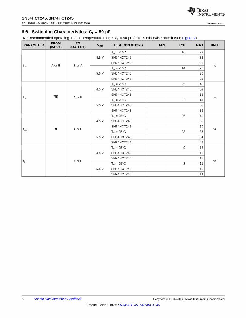
6.6 Switching Characteristics: CL = 50 pFover recommended operating free-air temperature range, CL = 50 pF (unless otherwise noted) (see Figure 2)
PARAMETER FROM(INPUT)
TO(OUTPUT) VCC TEST CONDITIONS MIN TYP MAX UNIT
tpd A or B B or A
4.5 VTA = 25°C 16 22
ns
SN54HCT245 33SN74HCT245 28
5.5 VTA = 25°C 14 20SN54HCT245 30SN74HCT245 25
ten OE A or B
4.5 VTA = 25°C 25 46
ns
SN54HCT245 69SN74HCT245 58
5.5 VTA = 25°C 22 41SN54HCT245 62SN74HCT245 52
tdis OE A or B
4.5 VTA = 25°C 26 40
ns
SN54HCT245 60SN74HCT245 50
5.5 VTA = 25°C 23 36SN54HCT245 54SN74HCT245 45
tt A or B
4.5 VTA = 25°C 9 12
ns
SN54HCT245 18SN74HCT245 15
5.5 VTA = 25°C 8 11SN54HCT245 16SN74HCT245 14
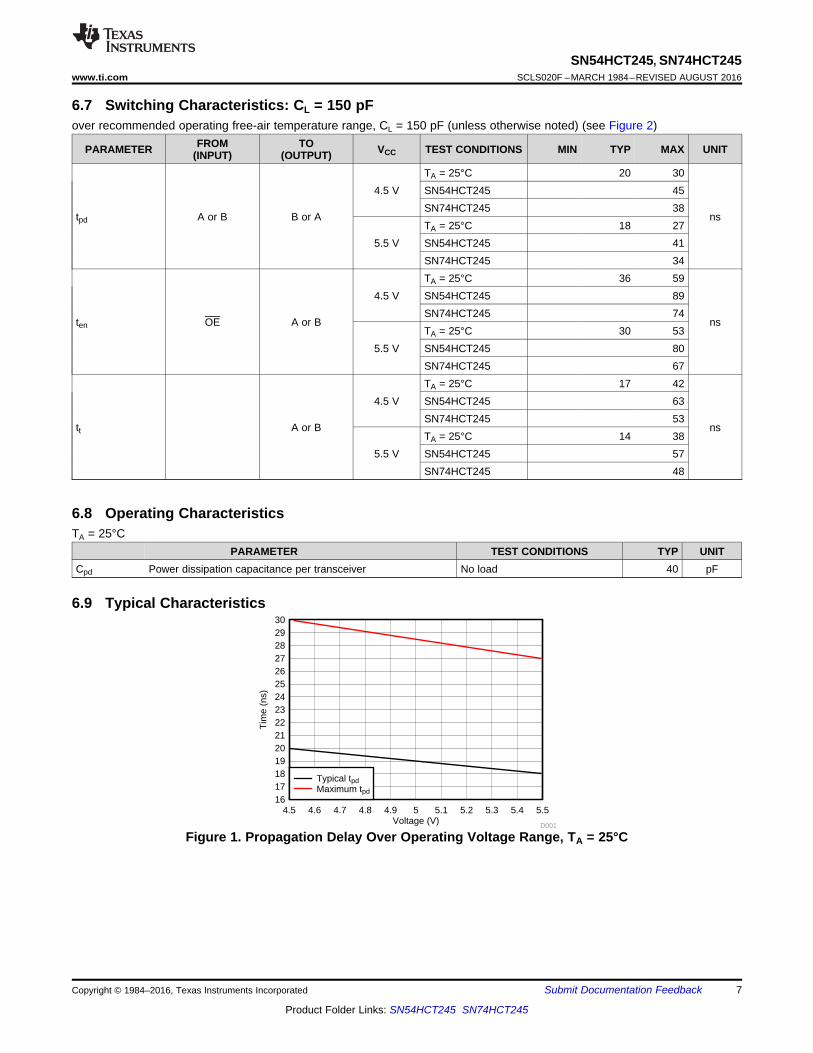
Voltage (V)
Tim
e (n
s)
4.5 4.6 4.7 4.8 4.9 5 5.1 5.2 5.3 5.4 5.5161718192021222324252627282930
D001
Typical tpdMaximum tpd
7
SN54HCT245, SN74HCT245www.ti.com SCLS020F –MARCH 1984–REVISED AUGUST 2016
Product Folder Links: SN54HCT245 SN74HCT245
Submit Documentation FeedbackCopyright © 1984–2016, Texas Instruments Incorporated
6.7 Switching Characteristics: CL = 150 pFover recommended operating free-air temperature range, CL = 150 pF (unless otherwise noted) (see Figure 2)
PARAMETER FROM(INPUT)
TO(OUTPUT) VCC TEST CONDITIONS MIN TYP MAX UNIT
tpd A or B B or A
4.5 VTA = 25°C 20 30
ns
SN54HCT245 45SN74HCT245 38
5.5 VTA = 25°C 18 27SN54HCT245 41SN74HCT245 34
ten OE A or B
4.5 VTA = 25°C 36 59
ns
SN54HCT245 89SN74HCT245 74
5.5 VTA = 25°C 30 53SN54HCT245 80SN74HCT245 67
tt A or B
4.5 VTA = 25°C 17 42
ns
SN54HCT245 63SN74HCT245 53
5.5 VTA = 25°C 14 38SN54HCT245 57SN74HCT245 48
6.8 Operating CharacteristicsTA = 25°C
PARAMETER TEST CONDITIONS TYP UNITCpd Power dissipation capacitance per transceiver No load 40 pF
6.9 Typical Characteristics
Figure 1. Propagation Delay Over Operating Voltage Range, TA = 25°C
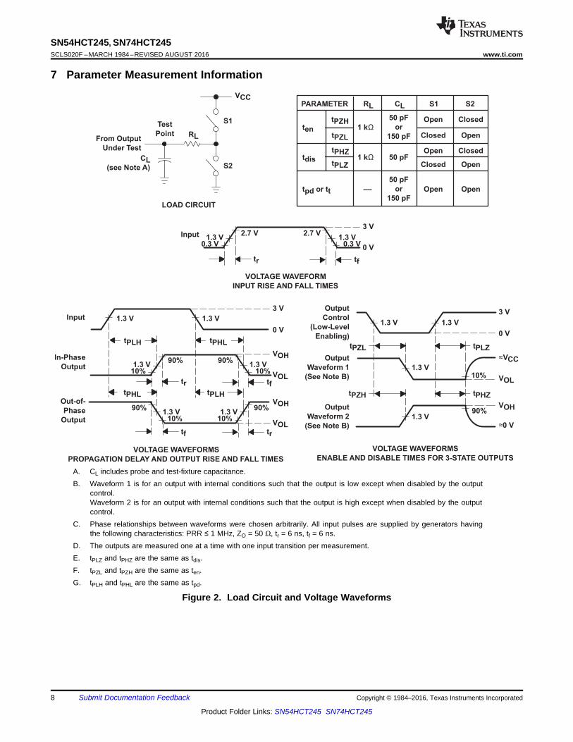
From Output
Under Test
RL
VCC
S1
S2
LOAD CIRCUIT
PARAMETER CL
tPZH
tpd or tt
tdis
tentPZL
tPHZ
tPLZ
1 kΩ
1 kΩ
50 pF
or
150 pF
50 pF
Open Closed
RL S1
Closed Open
S2
Open Closed
Closed Open
50 pF
or
150 pF
Open Open––
CL(see Note A)
Test
Point
VOLTAGE WAVEFORM
INPUT RISE AND FALL TIMES
1.3 V1.3 V0.3 V0.3 V
2.7 V 2.7 V3 V
0 V
tr tf
Input
VOLTAGE WAVEFORMS
PROPAGATION DELAY AND OUTPUT RISE AND FALL TIMES
1.3 V
1.3 V1.3 V10%10%
90% 90%
3 V
VOH
VOL
0 V
tr tf
Input
In-Phase
Output
1.3 V
tPLH tPHL
1.3 V 1.3 V10% 10%
90%90%VOH
VOLtrtf
tPHL tPLHOut-of-
Phase
Output
1.3 V
10%
90%
3 V
≈VCC
VOL
0 V
Output
Control
(Low-Level
Enabling)
Output
Waveform 1
(See Note B)
1.3 V
tPZL tPLZ
VOLTAGE WAVEFORMS
ENABLE AND DISABLE TIMES FOR 3-STATE OUTPUTS
VOH
≈0 V
1.3 V
1.3 V
tPZH tPHZ
Output
Waveform 2
(See Note B)
8
SN54HCT245, SN74HCT245SCLS020F –MARCH 1984–REVISED AUGUST 2016 www.ti.com
Product Folder Links: SN54HCT245 SN74HCT245
Submit Documentation Feedback Copyright © 1984–2016, Texas Instruments Incorporated
7 Parameter Measurement Information
A. CL includes probe and test-fixture capacitance.B. Waveform 1 is for an output with internal conditions such that the output is low except when disabled by the output
control.Waveform 2 is for an output with internal conditions such that the output is high except when disabled by the outputcontrol.
C. Phase relationships between waveforms were chosen arbitrarily. All input pulses are supplied by generators havingthe following characteristics: PRR ≤ 1 MHz, ZO = 50 Ω, tr = 6 ns, tf = 6 ns.
D. The outputs are measured one at a time with one input transition per measurement.E. tPLZ and tPHZ are the same as tdis.F. tPZL and tPZH are the same as ten.G. tPLH and tPHL are the same as tpd.
Figure 2. Load Circuit and Voltage Waveforms
DIR
OE
A1
B1
1
2
18
19
To Seven Other Channels
Copyright © 2016, Texas Instruments Incorporated
9
SN54HCT245, SN74HCT245www.ti.com SCLS020F –MARCH 1984–REVISED AUGUST 2016
Product Folder Links: SN54HCT245 SN74HCT245
Submit Documentation FeedbackCopyright © 1984–2016, Texas Instruments Incorporated
8 Detailed Description
8.1 OverviewThe SNx4HCT245 is a bidirectional buffer with direction control and active low output enable. This device iscommonly used in logic systems for isolation and increasing drive strength.
8.2 Functional Block Diagram
Figure 3. Logic Diagram (Positive Logic)
8.3 Feature DescriptionVoltage operating range from 4.5 V to 5.5 V is forgiving of 5-V power supply rail accuracy. Outputs can operateup to 15 LSTTL loads. This device has balanced propagation delay, typically 14 ns, and balanced output drive of±6 mA at 5 V. It has low power consumption of only 80-µA maximum static supply current. The center VCC andGND pin configurations minimize high-speed switching noise. Inputs are TTL-voltage compatible.
8.4 Device Functional ModesThis device is a standard '245 logic function. It has an active low output enable, a direction pin, and eightcommunication channels.
Table 1. Function TableINPUTS
OPERATIONOE DIRL L B data to A busL H A data to B busH X Isolation
SNx4HCT245DIR
Master DeviceLow Drive Strength(MCU, FPGA, CPU)
OE
A1
A2
A3
A4
A5
A6
A7
A8
B1
B2
B3
B4
B5
B6
B7
B8
Ribbon Cable
SNx4HC245DIR OE
A1
A2
A3
A4
A5
A6
A7
A8
B1
B2
B3
B4
B5
B6
B7
B8
Slave Deviceor
Back Plane
Copyright © 2016, Texas Instruments Incorporated
10
SN54HCT245, SN74HCT245SCLS020F –MARCH 1984–REVISED AUGUST 2016 www.ti.com
Product Folder Links: SN54HCT245 SN74HCT245
Submit Documentation Feedback Copyright © 1984–2016, Texas Instruments Incorporated
9 Application and Implementation
NOTEInformation in the following applications sections is not part of the TI componentspecification, and TI does not warrant its accuracy or completeness. TI’s customers areresponsible for determining suitability of components for their purposes. Customers shouldvalidate and test their design implementation to confirm system functionality.
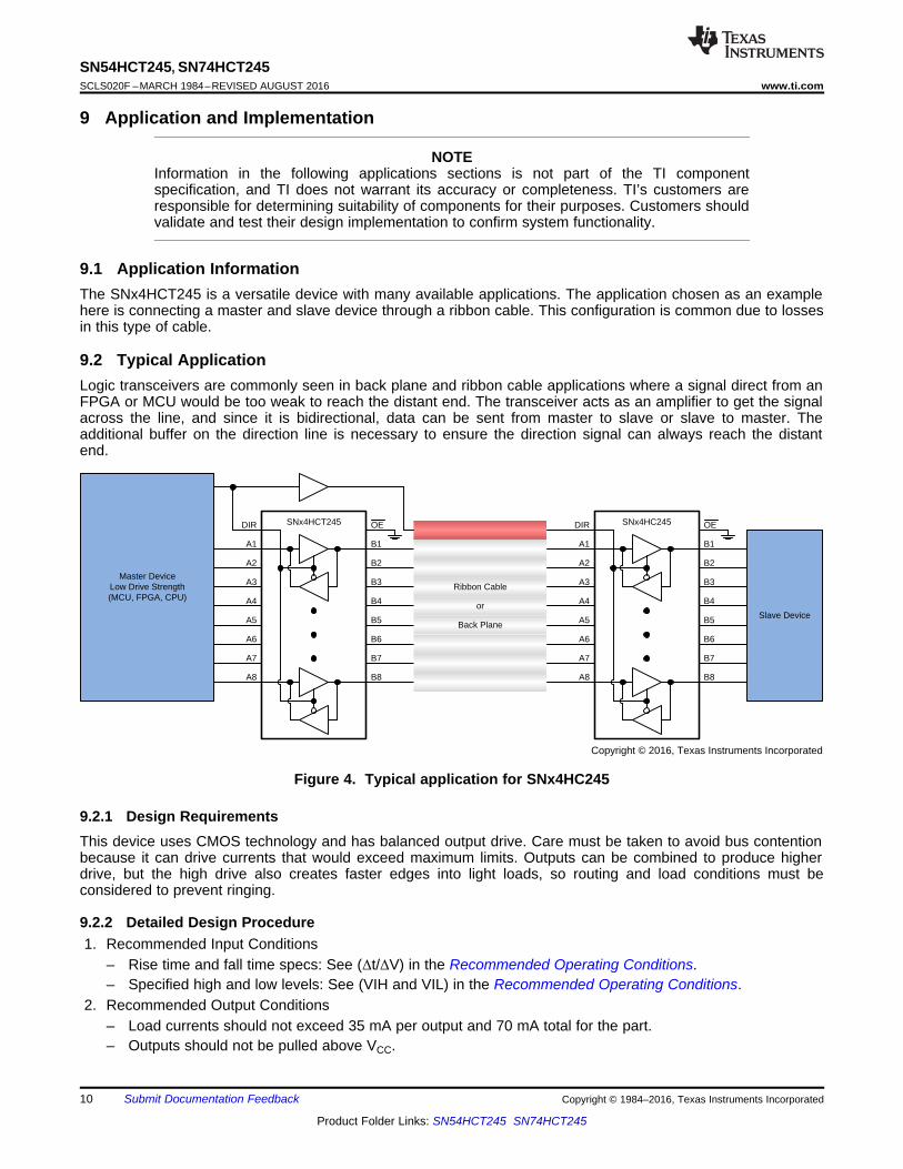
9.1 Application InformationThe SNx4HCT245 is a versatile device with many available applications. The application chosen as an examplehere is connecting a master and slave device through a ribbon cable. This configuration is common due to lossesin this type of cable.
9.2 Typical ApplicationLogic transceivers are commonly seen in back plane and ribbon cable applications where a signal direct from anFPGA or MCU would be too weak to reach the distant end. The transceiver acts as an amplifier to get the signalacross the line, and since it is bidirectional, data can be sent from master to slave or slave to master. Theadditional buffer on the direction line is necessary to ensure the direction signal can always reach the distantend.
Figure 4. Typical application for SNx4HC245
9.2.1 Design RequirementsThis device uses CMOS technology and has balanced output drive. Care must be taken to avoid bus contentionbecause it can drive currents that would exceed maximum limits. Outputs can be combined to produce higherdrive, but the high drive also creates faster edges into light loads, so routing and load conditions must beconsidered to prevent ringing.
9.2.2 Detailed Design Procedure1. Recommended Input Conditions
– Rise time and fall time specs: See (Δt/ΔV) in the Recommended Operating Conditions.– Specified high and low levels: See (VIH and VIL) in the Recommended Operating Conditions.
2. Recommended Output Conditions– Load currents should not exceed 35 mA per output and 70 mA total for the part.– Outputs should not be pulled above VCC.
Time (ns)
Vol
tage
(V
)
0 50 100 150 200 250 300 350 400 450 5000
0.5
1
1.5
2
2.5
3
3.5
4
4.5
5
5.5
D001
UnbufferedSN74HCT245
11
SN54HCT245, SN74HCT245www.ti.com SCLS020F –MARCH 1984–REVISED AUGUST 2016
Product Folder Links: SN54HCT245 SN74HCT245
Submit Documentation FeedbackCopyright © 1984–2016, Texas Instruments Incorporated
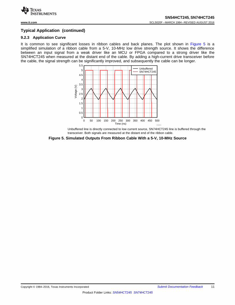
Typical Application (continued)9.2.3 Application CurveIt is common to see significant losses in ribbon cables and back planes. The plot shown in Figure 5 is asimplified simulation of a ribbon cable from a 5-V, 10-MHz low drive strength source. It shows the differencebetween an input signal from a weak driver like an MCU or FPGA compared to a strong driver like theSN74HCT245 when measured at the distant end of the cable. By adding a high-current drive transceiver beforethe cable, the signal strength can be significantly improved, and subsequently the cable can be longer.
Unbuffered line is directly connected to low current source, SN74HCT245 line is buffered through thetransceiver. Both signals are measured at the distant end of the ribbon cable.
Figure 5. Simulated Outputs From Ribbon Cable With a 5-V, 10-MHz Source
SNx4HCT245DIR OE
A1
A2
A3
A4
A5
A6
A7
A8
B1
B2
B3
B4
B5
B6
B7
B8
Slave DeviceMaster Device
10 k
10 k
10 k
10 k
12
SN54HCT245, SN74HCT245SCLS020F –MARCH 1984–REVISED AUGUST 2016 www.ti.com
Product Folder Links: SN54HCT245 SN74HCT245
Submit Documentation Feedback Copyright © 1984–2016, Texas Instruments Incorporated
10 Power Supply RecommendationsThe power supply can be any voltage between the MIN and MAX supply voltage rating located in theRecommended Operating Conditions. Each VCC pin must have a good bypass capacitor to prevent powerdisturbance. For devices with a single supply, 0.1 µF is recommended; if there are multiple VCC pins, then 0.01µF or 0.022 µF is recommended for each power pin. It is acceptable to parallel multiple bypass capacitors toreject different frequencies of noise. A 0.1 µF and a 1 µF are commonly used in parallel. The bypass capacitorshould be installed as close to the power pin as possible for best results.
11 Layout
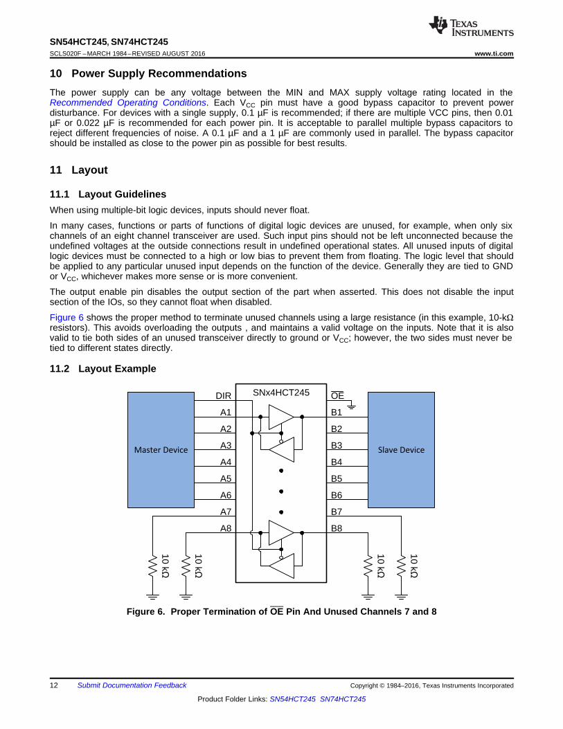
11.1 Layout GuidelinesWhen using multiple-bit logic devices, inputs should never float.
In many cases, functions or parts of functions of digital logic devices are unused, for example, when only sixchannels of an eight channel transceiver are used. Such input pins should not be left unconnected because theundefined voltages at the outside connections result in undefined operational states. All unused inputs of digitallogic devices must be connected to a high or low bias to prevent them from floating. The logic level that shouldbe applied to any particular unused input depends on the function of the device. Generally they are tied to GNDor VCC, whichever makes more sense or is more convenient.
The output enable pin disables the output section of the part when asserted. This does not disable the inputsection of the IOs, so they cannot float when disabled.
Figure 6 shows the proper method to terminate unused channels using a large resistance (in this example, 10-kΩresistors). This avoids overloading the outputs , and maintains a valid voltage on the inputs. Note that it is alsovalid to tie both sides of an unused transceiver directly to ground or VCC; however, the two sides must never betied to different states directly.
11.2 Layout Example
Figure 6. Proper Termination of OE Pin And Unused Channels 7 and 8
13
SN54HCT245, SN74HCT245www.ti.com SCLS020F –MARCH 1984–REVISED AUGUST 2016
Product Folder Links: SN54HCT245 SN74HCT245
Submit Documentation FeedbackCopyright © 1984–2016, Texas Instruments Incorporated
12 Device and Documentation Support
12.1 Documentation Support
12.1.1 Related DocumentationFor related documentation see the following:
Implications of Slow or Floating CMOS Inputs (SCBA004)
12.2 Related LinksThe table below lists quick access links. Categories include technical documents, support and communityresources, tools and software, and quick access to sample or buy.
Table 2. Related Links
PARTS PRODUCT FOLDER SAMPLE & BUY TECHNICALDOCUMENTS
TOOLS &SOFTWARE
SUPPORT &COMMUNITY
SN54HCT245 Click here Click here Click here Click here Click hereSN74HCT245 Click here Click here Click here Click here Click here
12.3 Receiving Notification of Documentation UpdatesTo receive notification of documentation updates, navigate to the device product folder on ti.com. In the upperright corner, click on Alert me to register and receive a weekly digest of any product information that haschanged. For change details, review the revision history included in any revised document.
12.4 Community ResourceThe following links connect to TI community resources. Linked contents are provided "AS IS" by the respectivecontributors. They do not constitute TI specifications and do not necessarily reflect TI's views; see TI's Terms ofUse.
TI E2E™ Online Community TI's Engineer-to-Engineer (E2E) Community. Created to foster collaborationamong engineers. At e2e.ti.com, you can ask questions, share knowledge, explore ideas and helpsolve problems with fellow engineers.
Design Support TI's Design Support Quickly find helpful E2E forums along with design support tools andcontact information for technical support.
12.5 TrademarksE2E is a trademark of Texas Instruments.All other trademarks are the property of their respective owners.
12.6 Electrostatic Discharge CautionThese devices have limited built-in ESD protection. The leads should be shorted together or the device placed in conductive foamduring storage or handling to prevent electrostatic damage to the MOS gates.
12.7 GlossarySLYZ022 — TI Glossary.
This glossary lists and explains terms, acronyms, and definitions.
13 Mechanical, Packaging, and Orderable InformationThe following pages include mechanical, packaging, and orderable information. This information is the mostcurrent data available for the designated devices. This data is subject to change without notice and revision ofthis document. For browser-based versions of this data sheet, refer to the left-hand navigation.
PACKAGE OPTION ADDENDUM
www.ti.com 17-Mar-2017
Addendum-Page 1
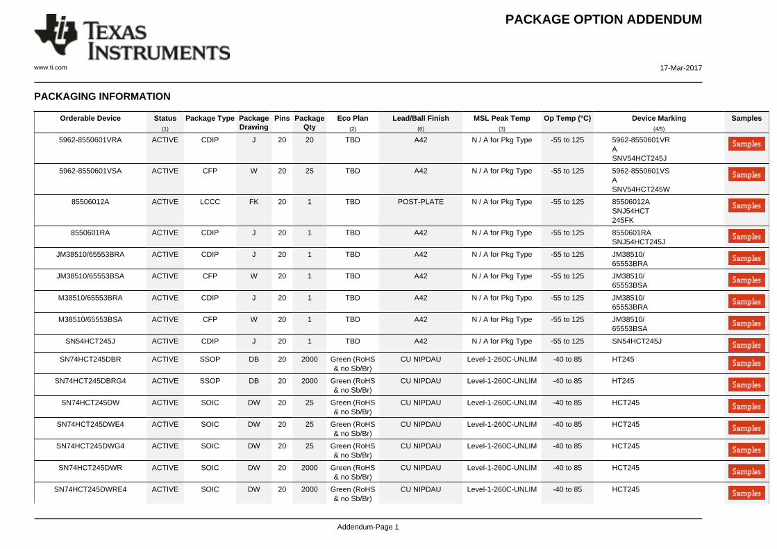
PACKAGING INFORMATION
Orderable Device Status(1)
Package Type PackageDrawing
Pins PackageQty
Eco Plan(2)
Lead/Ball Finish(6)
MSL Peak Temp(3)
Op Temp (°C) Device Marking(4/5)
Samples
5962-8550601VRA ACTIVE CDIP J 20 20 TBD A42 N / A for Pkg Type -55 to 125 5962-8550601VRASNV54HCT245J
5962-8550601VSA ACTIVE CFP W 20 25 TBD A42 N / A for Pkg Type -55 to 125 5962-8550601VSASNV54HCT245W
85506012A ACTIVE LCCC FK 20 1 TBD POST-PLATE N / A for Pkg Type -55 to 125 85506012ASNJ54HCT245FK
8550601RA ACTIVE CDIP J 20 1 TBD A42 N / A for Pkg Type -55 to 125 8550601RASNJ54HCT245J
JM38510/65553BRA ACTIVE CDIP J 20 1 TBD A42 N / A for Pkg Type -55 to 125 JM38510/65553BRA
JM38510/65553BSA ACTIVE CFP W 20 1 TBD A42 N / A for Pkg Type -55 to 125 JM38510/65553BSA
M38510/65553BRA ACTIVE CDIP J 20 1 TBD A42 N / A for Pkg Type -55 to 125 JM38510/65553BRA
M38510/65553BSA ACTIVE CFP W 20 1 TBD A42 N / A for Pkg Type -55 to 125 JM38510/65553BSA
SN54HCT245J ACTIVE CDIP J 20 1 TBD A42 N / A for Pkg Type -55 to 125 SN54HCT245J
SN74HCT245DBR ACTIVE SSOP DB 20 2000 Green (RoHS& no Sb/Br)
CU NIPDAU Level-1-260C-UNLIM -40 to 85 HT245
SN74HCT245DBRG4 ACTIVE SSOP DB 20 2000 Green (RoHS& no Sb/Br)
CU NIPDAU Level-1-260C-UNLIM -40 to 85 HT245
SN74HCT245DW ACTIVE SOIC DW 20 25 Green (RoHS& no Sb/Br)
CU NIPDAU Level-1-260C-UNLIM -40 to 85 HCT245
SN74HCT245DWE4 ACTIVE SOIC DW 20 25 Green (RoHS& no Sb/Br)
CU NIPDAU Level-1-260C-UNLIM -40 to 85 HCT245
SN74HCT245DWG4 ACTIVE SOIC DW 20 25 Green (RoHS& no Sb/Br)
CU NIPDAU Level-1-260C-UNLIM -40 to 85 HCT245
SN74HCT245DWR ACTIVE SOIC DW 20 2000 Green (RoHS& no Sb/Br)
CU NIPDAU Level-1-260C-UNLIM -40 to 85 HCT245
SN74HCT245DWRE4 ACTIVE SOIC DW 20 2000 Green (RoHS& no Sb/Br)
CU NIPDAU Level-1-260C-UNLIM -40 to 85 HCT245
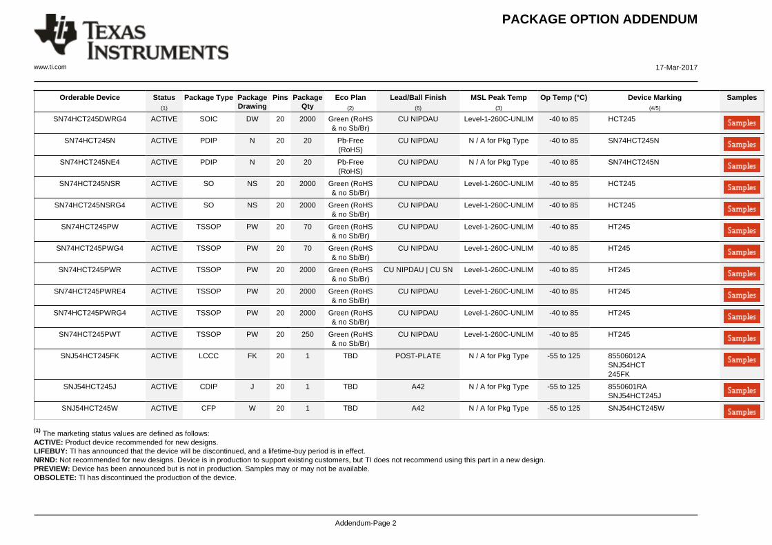
PACKAGE OPTION ADDENDUM
www.ti.com 17-Mar-2017
Addendum-Page 2
Orderable Device Status(1)
Package Type PackageDrawing
Pins PackageQty
Eco Plan(2)
Lead/Ball Finish(6)
MSL Peak Temp(3)
Op Temp (°C) Device Marking(4/5)
Samples
SN74HCT245DWRG4 ACTIVE SOIC DW 20 2000 Green (RoHS& no Sb/Br)
CU NIPDAU Level-1-260C-UNLIM -40 to 85 HCT245
SN74HCT245N ACTIVE PDIP N 20 20 Pb-Free(RoHS)
CU NIPDAU N / A for Pkg Type -40 to 85 SN74HCT245N
SN74HCT245NE4 ACTIVE PDIP N 20 20 Pb-Free(RoHS)
CU NIPDAU N / A for Pkg Type -40 to 85 SN74HCT245N
SN74HCT245NSR ACTIVE SO NS 20 2000 Green (RoHS& no Sb/Br)
CU NIPDAU Level-1-260C-UNLIM -40 to 85 HCT245
SN74HCT245NSRG4 ACTIVE SO NS 20 2000 Green (RoHS& no Sb/Br)
CU NIPDAU Level-1-260C-UNLIM -40 to 85 HCT245
SN74HCT245PW ACTIVE TSSOP PW 20 70 Green (RoHS& no Sb/Br)
CU NIPDAU Level-1-260C-UNLIM -40 to 85 HT245
SN74HCT245PWG4 ACTIVE TSSOP PW 20 70 Green (RoHS& no Sb/Br)
CU NIPDAU Level-1-260C-UNLIM -40 to 85 HT245
SN74HCT245PWR ACTIVE TSSOP PW 20 2000 Green (RoHS& no Sb/Br)
CU NIPDAU | CU SN Level-1-260C-UNLIM -40 to 85 HT245
SN74HCT245PWRE4 ACTIVE TSSOP PW 20 2000 Green (RoHS& no Sb/Br)
CU NIPDAU Level-1-260C-UNLIM -40 to 85 HT245
SN74HCT245PWRG4 ACTIVE TSSOP PW 20 2000 Green (RoHS& no Sb/Br)
CU NIPDAU Level-1-260C-UNLIM -40 to 85 HT245
SN74HCT245PWT ACTIVE TSSOP PW 20 250 Green (RoHS& no Sb/Br)
CU NIPDAU Level-1-260C-UNLIM -40 to 85 HT245
SNJ54HCT245FK ACTIVE LCCC FK 20 1 TBD POST-PLATE N / A for Pkg Type -55 to 125 85506012ASNJ54HCT245FK
SNJ54HCT245J ACTIVE CDIP J 20 1 TBD A42 N / A for Pkg Type -55 to 125 8550601RASNJ54HCT245J
SNJ54HCT245W ACTIVE CFP W 20 1 TBD A42 N / A for Pkg Type -55 to 125 SNJ54HCT245W
(1) The marketing status values are defined as follows:ACTIVE: Product device recommended for new designs.LIFEBUY: TI has announced that the device will be discontinued, and a lifetime-buy period is in effect.NRND: Not recommended for new designs. Device is in production to support existing customers, but TI does not recommend using this part in a new design.PREVIEW: Device has been announced but is not in production. Samples may or may not be available.OBSOLETE: TI has discontinued the production of the device.
PACKAGE OPTION ADDENDUM
www.ti.com 17-Mar-2017
Addendum-Page 3
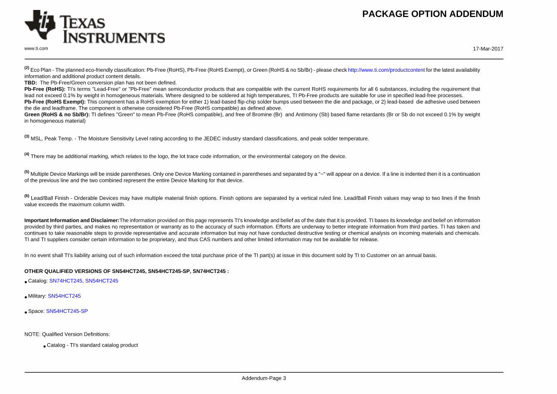
(2) Eco Plan - The planned eco-friendly classification: Pb-Free (RoHS), Pb-Free (RoHS Exempt), or Green (RoHS & no Sb/Br) - please check http://www.ti.com/productcontent for the latest availabilityinformation and additional product content details.TBD: The Pb-Free/Green conversion plan has not been defined.Pb-Free (RoHS): TI's terms "Lead-Free" or "Pb-Free" mean semiconductor products that are compatible with the current RoHS requirements for all 6 substances, including the requirement thatlead not exceed 0.1% by weight in homogeneous materials. Where designed to be soldered at high temperatures, TI Pb-Free products are suitable for use in specified lead-free processes.Pb-Free (RoHS Exempt): This component has a RoHS exemption for either 1) lead-based flip-chip solder bumps used between the die and package, or 2) lead-based die adhesive used betweenthe die and leadframe. The component is otherwise considered Pb-Free (RoHS compatible) as defined above.Green (RoHS & no Sb/Br): TI defines "Green" to mean Pb-Free (RoHS compatible), and free of Bromine (Br) and Antimony (Sb) based flame retardants (Br or Sb do not exceed 0.1% by weightin homogeneous material)
(3) MSL, Peak Temp. - The Moisture Sensitivity Level rating according to the JEDEC industry standard classifications, and peak solder temperature.
(4) There may be additional marking, which relates to the logo, the lot trace code information, or the environmental category on the device.
(5) Multiple Device Markings will be inside parentheses. Only one Device Marking contained in parentheses and separated by a "~" will appear on a device. If a line is indented then it is a continuationof the previous line and the two combined represent the entire Device Marking for that device.
(6) Lead/Ball Finish - Orderable Devices may have multiple material finish options. Finish options are separated by a vertical ruled line. Lead/Ball Finish values may wrap to two lines if the finishvalue exceeds the maximum column width.
Important Information and Disclaimer:The information provided on this page represents TI's knowledge and belief as of the date that it is provided. TI bases its knowledge and belief on informationprovided by third parties, and makes no representation or warranty as to the accuracy of such information. Efforts are underway to better integrate information from third parties. TI has taken andcontinues to take reasonable steps to provide representative and accurate information but may not have conducted destructive testing or chemical analysis on incoming materials and chemicals.TI and TI suppliers consider certain information to be proprietary, and thus CAS numbers and other limited information may not be available for release.
In no event shall TI's liability arising out of such information exceed the total purchase price of the TI part(s) at issue in this document sold by TI to Customer on an annual basis.
OTHER QUALIFIED VERSIONS OF SN54HCT245, SN54HCT245-SP, SN74HCT245 :
• Catalog: SN74HCT245, SN54HCT245
• Military: SN54HCT245
• Space: SN54HCT245-SP
NOTE: Qualified Version Definitions:
• Catalog - TI's standard catalog product
PACKAGE OPTION ADDENDUM
www.ti.com 17-Mar-2017
Addendum-Page 4
• Military - QML certified for Military and Defense Applications
• Space - Radiation tolerant, ceramic packaging and qualified for use in Space-based application
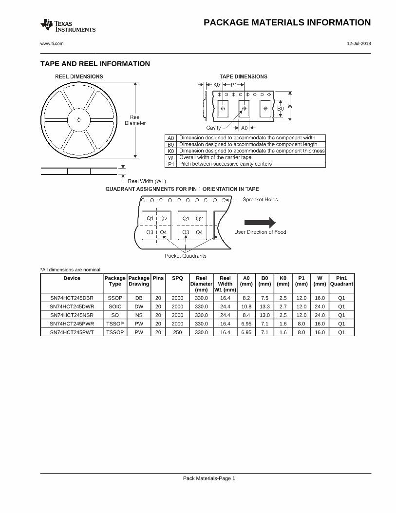
TAPE AND REEL INFORMATION
*All dimensions are nominal
Device PackageType
PackageDrawing
Pins SPQ ReelDiameter
(mm)
ReelWidth
W1 (mm)
A0(mm)
B0(mm)
K0(mm)
P1(mm)
W(mm)
Pin1Quadrant
SN74HCT245DBR SSOP DB 20 2000 330.0 16.4 8.2 7.5 2.5 12.0 16.0 Q1
SN74HCT245DWR SOIC DW 20 2000 330.0 24.4 10.8 13.3 2.7 12.0 24.0 Q1
SN74HCT245NSR SO NS 20 2000 330.0 24.4 8.4 13.0 2.5 12.0 24.0 Q1
SN74HCT245PWR TSSOP PW 20 2000 330.0 16.4 6.95 7.1 1.6 8.0 16.0 Q1
SN74HCT245PWT TSSOP PW 20 250 330.0 16.4 6.95 7.1 1.6 8.0 16.0 Q1
PACKAGE MATERIALS INFORMATION
www.ti.com 12-Jul-2018
Pack Materials-Page 1
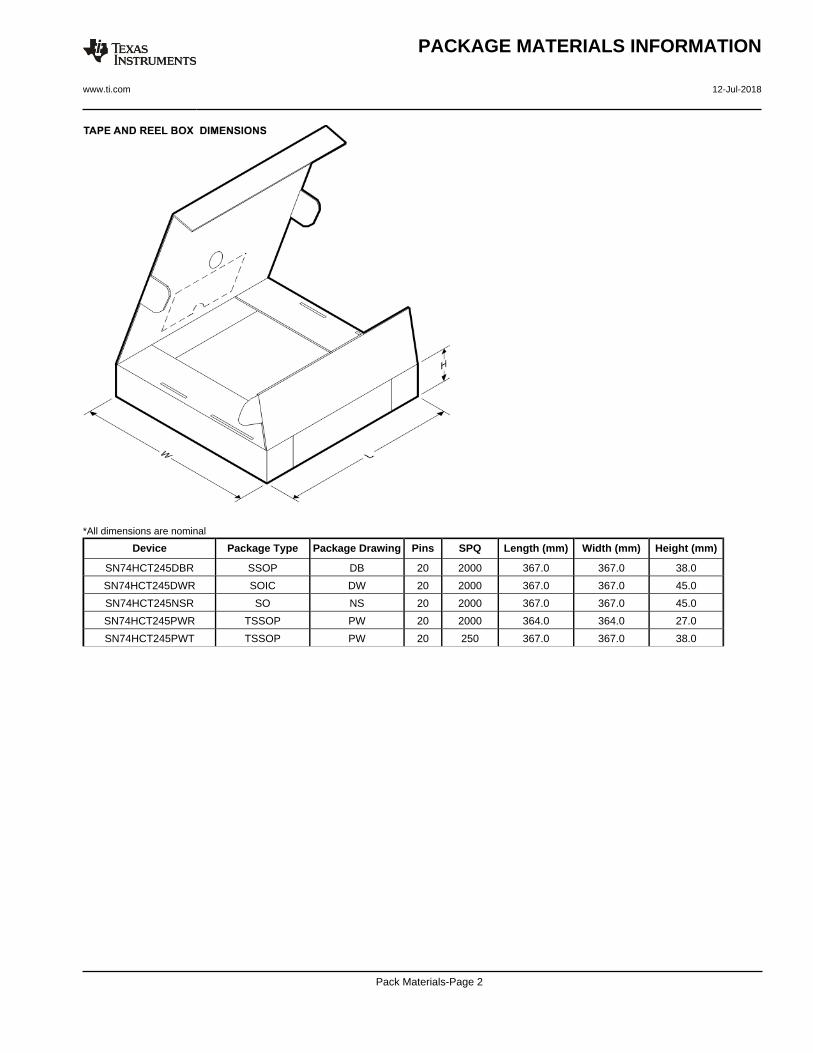
*All dimensions are nominal
Device Package Type Package Drawing Pins SPQ Length (mm) Width (mm) Height (mm)
SN74HCT245DBR SSOP DB 20 2000 367.0 367.0 38.0
SN74HCT245DWR SOIC DW 20 2000 367.0 367.0 45.0
SN74HCT245NSR SO NS 20 2000 367.0 367.0 45.0
SN74HCT245PWR TSSOP PW 20 2000 364.0 364.0 27.0
SN74HCT245PWT TSSOP PW 20 250 367.0 367.0 38.0
PACKAGE MATERIALS INFORMATION
www.ti.com 12-Jul-2018
Pack Materials-Page 2
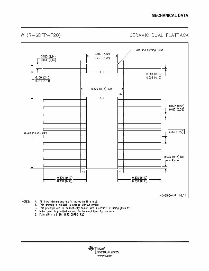
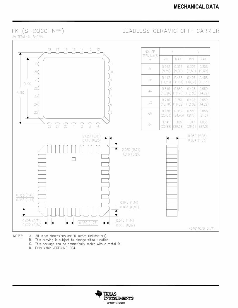
MECHANICAL DATA
MSSO002E – JANUARY 1995 – REVISED DECEMBER 2001
POST OFFICE BOX 655303 • DALLAS, TEXAS 75265
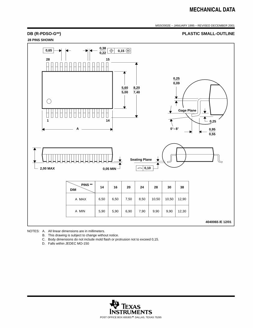
DB (R-PDSO-G**) PLASTIC SMALL-OUTLINE
4040065 /E 12/01
28 PINS SHOWN
Gage Plane
8,207,40
0,550,95
0,25
38
12,90
12,30
28
10,50
24
8,50
Seating Plane
9,907,90
30
10,50
9,90
0,38
5,605,00
15
0,22
14
A
28
1
2016
6,506,50
14
0,05 MIN
5,905,90
DIM
A MAX
A MIN
PINS **
2,00 MAX
6,90
7,50
0,65 M0,15
0°–8°
0,10
0,090,25
NOTES: A. All linear dimensions are in millimeters.B. This drawing is subject to change without notice.C. Body dimensions do not include mold flash or protrusion not to exceed 0,15.D. Falls within JEDEC MO-150
www.ti.com
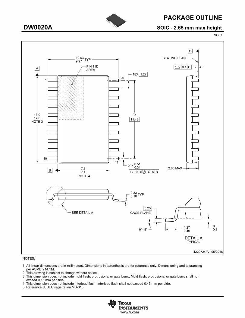
PACKAGE OUTLINE
C
TYP10.639.97
2.65 MAX
18X 1.27
20X 0.510.31
2X11.43
TYP0.330.10
0 - 80.30.1
0.25GAGE PLANE
1.270.40
A
NOTE 3
13.012.6
B 7.67.4
4220724/A 05/2016
SOIC - 2.65 mm max heightDW0020ASOIC
NOTES: 1. All linear dimensions are in millimeters. Dimensions in parenthesis are for reference only. Dimensioning and tolerancing per ASME Y14.5M. 2. This drawing is subject to change without notice. 3. This dimension does not include mold flash, protrusions, or gate burrs. Mold flash, protrusions, or gate burrs shall not exceed 0.15 mm per side. 4. This dimension does not include interlead flash. Interlead flash shall not exceed 0.43 mm per side.5. Reference JEDEC registration MS-013.
120
0.25 C A B
1110
PIN 1 IDAREA
NOTE 4
SEATING PLANE
0.1 C
SEE DETAIL A
DETAIL ATYPICAL
SCALE 1.200
www.ti.com
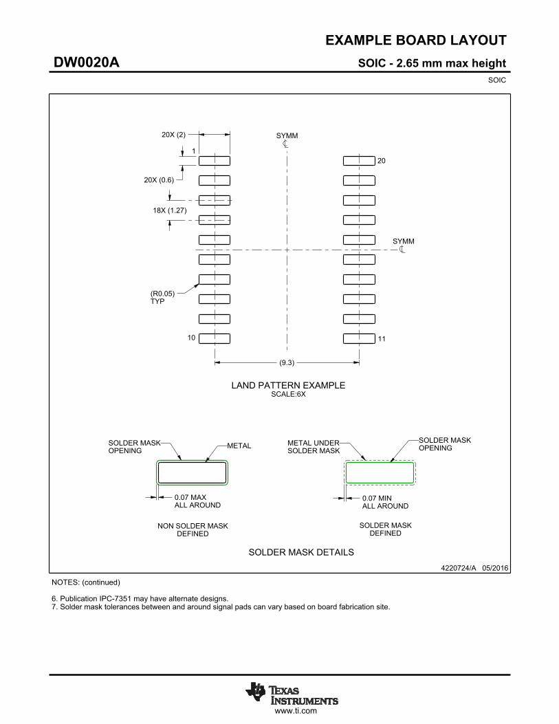
EXAMPLE BOARD LAYOUT
(9.3)
0.07 MAXALL AROUND
0.07 MINALL AROUND
20X (2)
20X (0.6)
18X (1.27)
(R )TYP
0.05
4220724/A 05/2016
SOIC - 2.65 mm max heightDW0020ASOIC
SYMM
SYMM
LAND PATTERN EXAMPLESCALE:6X
1
10 11
20
NOTES: (continued) 6. Publication IPC-7351 may have alternate designs. 7. Solder mask tolerances between and around signal pads can vary based on board fabrication site.
METALSOLDER MASKOPENING
NON SOLDER MASKDEFINED
SOLDER MASK DETAILS
SOLDER MASKOPENING
METAL UNDERSOLDER MASK
SOLDER MASKDEFINED
www.ti.com
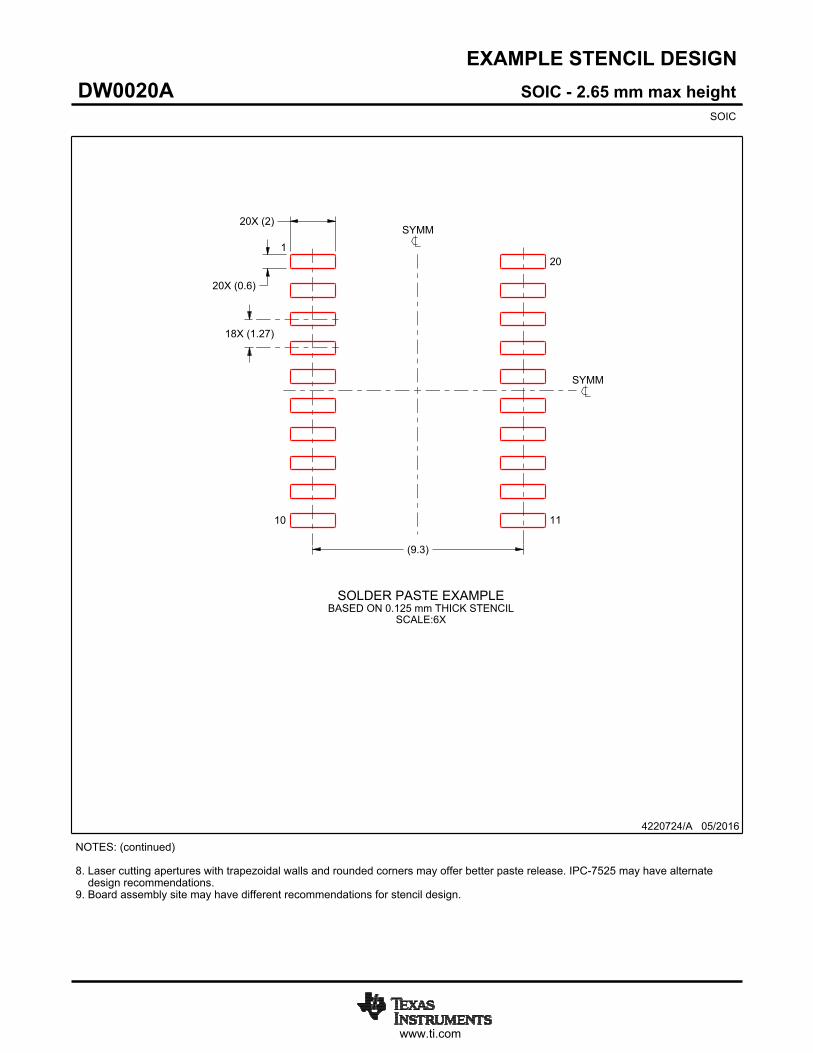
EXAMPLE STENCIL DESIGN
(9.3)
18X (1.27)
20X (0.6)
20X (2)
4220724/A 05/2016
SOIC - 2.65 mm max heightDW0020ASOIC
NOTES: (continued) 8. Laser cutting apertures with trapezoidal walls and rounded corners may offer better paste release. IPC-7525 may have alternate design recommendations. 9. Board assembly site may have different recommendations for stencil design.
SYMM
SYMM
1
10 11
20
SOLDER PASTE EXAMPLEBASED ON 0.125 mm THICK STENCIL
SCALE:6X
IMPORTANT NOTICE
Texas Instruments Incorporated (TI) reserves the right to make corrections, enhancements, improvements and other changes to itssemiconductor products and services per JESD46, latest issue, and to discontinue any product or service per JESD48, latest issue. Buyersshould obtain the latest relevant information before placing orders and should verify that such information is current and complete.TI’s published terms of sale for semiconductor products (http://www.ti.com/sc/docs/stdterms.htm) apply to the sale of packaged integratedcircuit products that TI has qualified and released to market. Additional terms may apply to the use or sale of other types of TI products andservices.Reproduction of significant portions of TI information in TI data sheets is permissible only if reproduction is without alteration and isaccompanied by all associated warranties, conditions, limitations, and notices. TI is not responsible or liable for such reproduceddocumentation. Information of third parties may be subject to additional restrictions. Resale of TI products or services with statementsdifferent from or beyond the parameters stated by TI for that product or service voids all express and any implied warranties for theassociated TI product or service and is an unfair and deceptive business practice. TI is not responsible or liable for any such statements.Buyers and others who are developing systems that incorporate TI products (collectively, “Designers”) understand and agree that Designersremain responsible for using their independent analysis, evaluation and judgment in designing their applications and that Designers havefull and exclusive responsibility to assure the safety of Designers' applications and compliance of their applications (and of all TI productsused in or for Designers’ applications) with all applicable regulations, laws and other applicable requirements. Designer represents that, withrespect to their applications, Designer has all the necessary expertise to create and implement safeguards that (1) anticipate dangerousconsequences of failures, (2) monitor failures and their consequences, and (3) lessen the likelihood of failures that might cause harm andtake appropriate actions. Designer agrees that prior to using or distributing any applications that include TI products, Designer willthoroughly test such applications and the functionality of such TI products as used in such applications.TI’s provision of technical, application or other design advice, quality characterization, reliability data or other services or information,including, but not limited to, reference designs and materials relating to evaluation modules, (collectively, “TI Resources”) are intended toassist designers who are developing applications that incorporate TI products; by downloading, accessing or using TI Resources in anyway, Designer (individually or, if Designer is acting on behalf of a company, Designer’s company) agrees to use any particular TI Resourcesolely for this purpose and subject to the terms of this Notice.TI’s provision of TI Resources does not expand or otherwise alter TI’s applicable published warranties or warranty disclaimers for TIproducts, and no additional obligations or liabilities arise from TI providing such TI Resources. TI reserves the right to make corrections,enhancements, improvements and other changes to its TI Resources. TI has not conducted any testing other than that specificallydescribed in the published documentation for a particular TI Resource.Designer is authorized to use, copy and modify any individual TI Resource only in connection with the development of applications thatinclude the TI product(s) identified in such TI Resource. NO OTHER LICENSE, EXPRESS OR IMPLIED, BY ESTOPPEL OR OTHERWISETO ANY OTHER TI INTELLECTUAL PROPERTY RIGHT, AND NO LICENSE TO ANY TECHNOLOGY OR INTELLECTUAL PROPERTYRIGHT OF TI OR ANY THIRD PARTY IS GRANTED HEREIN, including but not limited to any patent right, copyright, mask work right, orother intellectual property right relating to any combination, machine, or process in which TI products or services are used. Informationregarding or referencing third-party products or services does not constitute a license to use such products or services, or a warranty orendorsement thereof. Use of TI Resources may require a license from a third party under the patents or other intellectual property of thethird party, or a license from TI under the patents or other intellectual property of TI.TI RESOURCES ARE PROVIDED “AS IS” AND WITH ALL FAULTS. TI DISCLAIMS ALL OTHER WARRANTIES ORREPRESENTATIONS, EXPRESS OR IMPLIED, REGARDING RESOURCES OR USE THEREOF, INCLUDING BUT NOT LIMITED TOACCURACY OR COMPLETENESS, TITLE, ANY EPIDEMIC FAILURE WARRANTY AND ANY IMPLIED WARRANTIES OFMERCHANTABILITY, FITNESS FOR A PARTICULAR PURPOSE, AND NON-INFRINGEMENT OF ANY THIRD PARTY INTELLECTUALPROPERTY RIGHTS. TI SHALL NOT BE LIABLE FOR AND SHALL NOT DEFEND OR INDEMNIFY DESIGNER AGAINST ANY CLAIM,INCLUDING BUT NOT LIMITED TO ANY INFRINGEMENT CLAIM THAT RELATES TO OR IS BASED ON ANY COMBINATION OFPRODUCTS EVEN IF DESCRIBED IN TI RESOURCES OR OTHERWISE. IN NO EVENT SHALL TI BE LIABLE FOR ANY ACTUAL,DIRECT, SPECIAL, COLLATERAL, INDIRECT, PUNITIVE, INCIDENTAL, CONSEQUENTIAL OR EXEMPLARY DAMAGES INCONNECTION WITH OR ARISING OUT OF TI RESOURCES OR USE THEREOF, AND REGARDLESS OF WHETHER TI HAS BEENADVISED OF THE POSSIBILITY OF SUCH DAMAGES.Unless TI has explicitly designated an individual product as meeting the requirements of a particular industry standard (e.g., ISO/TS 16949and ISO 26262), TI is not responsible for any failure to meet such industry standard requirements.Where TI specifically promotes products as facilitating functional safety or as compliant with industry functional safety standards, suchproducts are intended to help enable customers to design and create their own applications that meet applicable functional safety standardsand requirements. Using products in an application does not by itself establish any safety features in the application. Designers mustensure compliance with safety-related requirements and standards applicable to their applications. Designer may not use any TI products inlife-critical medical equipment unless authorized officers of the parties have executed a special contract specifically governing such use.Life-critical medical equipment is medical equipment where failure of such equipment would cause serious bodily injury or death (e.g., lifesupport, pacemakers, defibrillators, heart pumps, neurostimulators, and implantables). Such equipment includes, without limitation, allmedical devices identified by the U.S. Food and Drug Administration as Class III devices and equivalent classifications outside the U.S.TI may expressly designate certain products as completing a particular qualification (e.g., Q100, Military Grade, or Enhanced Product).Designers agree that it has the necessary expertise to select the product with the appropriate qualification designation for their applicationsand that proper product selection is at Designers’ own risk. Designers are solely responsible for compliance with all legal and regulatoryrequirements in connection with such selection.Designer will fully indemnify TI and its representatives against any damages, costs, losses, and/or liabilities arising out of Designer’s non-compliance with the terms and provisions of this Notice.
Mailing Address: Texas Instruments, Post Office Box 655303, Dallas, Texas 75265Copyright © 2018, Texas Instruments Incorporated