Embed Size (px)
Citation preview
SN65ALS176, SN75ALS176, SN75ALS176A, SN75ALS176BDIFFERENTIAL BUS TRANSCEIVERS
SLLS040H – AUGUST 1987 – REVISED JUNE 2000
1POST OFFICE BOX 655303 • DALLAS, TEXAS 75265
Meet or Exceed the Requirements ofTIA/EIA-422-B, TIA/EIA-485-A † and ITURecommendations V.11 and X.27
Operate at Data Rates up to 35 Mbaud
Four Skew Limits Available:SN65ALS176 . . . 15 nsSN75ALS176 . . . 10 nsSN75ALS176A . . . 7.5 nsSN75ALS176B . . . 5 ns
Designed for Multipoint Transmission onLong Bus Lines in Noisy Environments
Low Supply-Current Requirements. . . 30 mA Max
Wide Positive and Negative Input/OutputBus-Voltage Ranges
Thermal Shutdown Protection
Driver Positive and Negative CurrentLimiting
Receiver Input Hysteresis
Glitch-Free Power-Up and Power-DownProtection
Receiver Open-Circuit Fail-Safe Design
description
The SN65ALS176 and SN75ALS176 series differential bus transceivers are designed for bidirectional datacommunication on multipoint bus transmission lines. They are designed for balanced transmission lines andmeet TIA/EIA-422-B, TIA/EIA-485-A, and ITU Recommendations V.11 and X.27.
The SN65ALS176 and SN75ALS176 series combine a 3-state, differential line driver and a differential input linereceiver, both of which operate from a single 5-V power supply. The driver and receiver have active-high andactive-low enables, respectively, that can be connected together externally to function as a direction control.The driver differential outputs and the receiver differential inputs are connected internally to form a differentialinput/output (I/O) bus port that is designed to offer minimum loading to the bus when the driver is disabled orVCC = 0. This port features wide positive and negative common-mode voltage ranges, making the devicesuitable for party-line applications.
The SN65ALS176 is characterized for operation from –40°C to 85°C. The SN75ALS176 series is characterizedfor operation from 0°C to 70°C.
Copyright 2000, Texas Instruments IncorporatedPRODUCTION DATA information is current as of publication date.Products conform to specifications per the terms of Texas Instrumentsstandard warranty. Production processing does not necessarily includetesting of all parameters.
Please be aware that an important notice concerning availability, standard warranty, and use in critical applications ofTexas Instruments semiconductor products and disclaimers thereto appears at the end of this data sheet.
1
2
3
4
8
7
6
5
RREDE
D
VCCBAGND
D OR P PACKAGE(TOP VIEW)
† These devices meet or exceed the requirements of TIA/EIA-485-A, except for the Generator Contention Test (para. 3.4.2) and the GeneratorCurrent Limit (para. 3.4.3). The applied test voltage ranges are –6 V to 8 V for the SN75ALS176, SN75ALS176A, and SN75ALS176B and–4 V to 8 V for the SN65ALS180.

SN65ALS176, SN75ALS176, SN75ALS176A, SN75ALS176BDIFFERENTIAL BUS TRANSCEIVERS
SLLS040H – AUGUST 1987 – REVISED JUNE 2000
2 POST OFFICE BOX 655303 • DALLAS, TEXAS 75265
AVAILABLE OPTIONS
†PACKAGED DEVICES
TA tsk(lim) † SMALL OUTLINE(D)‡
PLASTIC DIP(P)
0°C to 70°C107.55
SN75ALS176DSN75ALS176ADSN75ALS176BD
SN75ALS176PSN75ALS176APSN75ALS176BP
–40°C to 85°C 15 SN65ALS176D SN65ALS176P
† This is the maximum range that the driver or receiver delay times vary overtemperature, VCC, and process (device to device).
‡ The D package is available taped and reeled. Add the suffix R to the devicetype (e.g., SN75ALS176DR).
Function Tables
DRIVER
INPUT ENABLE OUTPUTSD DE A B
H H H L
L H L H
X L Z Z
H = high level, L = low level, X = irrelevant,Z = high impedance
RECEIVER
DIFFERENTIALINPUTS
A–B
ENABLERE
OUTPUTR
VID ≥ 0.2 V L H
–0.2 V < VID < 0.2 V L ?
VID ≤ –0.2 V L L
X H Z
Inputs open L H
H = high level, L = low level, X = irrelevant,Z = high impedance
logic symbol §
§ This symbol is in accordance with ANSI/IEEE Std 91-1984 andIEC Publication 617-12.
4D
EN22
R1
A6
B7
EN13
DE
RE
2
1
1
logic diagram (positive logic)
3
4
2
16
7
DE
D
RE
RA
BBus

SN65ALS176, SN75ALS176, SN75ALS176A, SN75ALS176BDIFFERENTIAL BUS TRANSCEIVERS
SLLS040H – AUGUST 1987 – REVISED JUNE 2000
3POST OFFICE BOX 655303 • DALLAS, TEXAS 75265
schematics of inputs and outputs
EQUIVALENT OF EACH INPUT
Driver Input: R (eq) = 3 kΩ NOMEnable Inputs: R (eq) = 8 kΩ NOMR(eq) = equivalent resistor
TYPICAL OF A AND B I/O PORTS TYPICAL OF RECEIVER OUTPUT
Output
85 ΩNOM
VCC
180 kΩNOMConnectedon B Port
1.1 kΩNOM
3 kΩNOM
18 kΩNOM
180 kΩNOMConnectedon A Port
A or B
R(eq)
VCC
Input
VCC
absolute maximum ratings over operating free-air temperature range (unless otherwise noted) †
Supply voltage, VCC (see Note 1) 7 V. . . . . . . . . . . . . . . . . . . . . . . . . . . . . . . . . . . . . . . . . . . . . . . . . . . . . . . . . . . . . Voltage range at any bus terminal –7 V to 12 V. . . . . . . . . . . . . . . . . . . . . . . . . . . . . . . . . . . . . . . . . . . . . . . . . . . . . Enable input voltage, VI 5.5 V. . . . . . . . . . . . . . . . . . . . . . . . . . . . . . . . . . . . . . . . . . . . . . . . . . . . . . . . . . . . . . . . . . . . Package thermal impedance, θJA (see Note 2): D package 97°C/W. . . . . . . . . . . . . . . . . . . . . . . . . . . . . . . . . . .
P package 85°C/W. . . . . . . . . . . . . . . . . . . . . . . . . . . . . . . . . . . Lead temperature 1,6 mm (1/16 inch) from case for 10 seconds 260°C. . . . . . . . . . . . . . . . . . . . . . . . . . . . . . . Storage temperature range, Tstg –65°C to 150°C. . . . . . . . . . . . . . . . . . . . . . . . . . . . . . . . . . . . . . . . . . . . . . . . . . .
† Stresses beyond those listed under “absolute maximum ratings” may cause permanent damage to the device. These are stress ratings only, andfunctional operation of the device at these or any other conditions beyond those indicated under “recommended operating conditions” is notimplied. Exposure to absolute-maximum-rated conditions for extended periods may affect device reliability.
NOTES: 1. All voltage values, except differential I/O bus voltage, are with respect to network ground terminal.2. The package thermal impedance is calculated in accordance with JESD 51.

SN65ALS176, SN75ALS176, SN75ALS176A, SN75ALS176BDIFFERENTIAL BUS TRANSCEIVERS
SLLS040H – AUGUST 1987 – REVISED JUNE 2000
4 POST OFFICE BOX 655303 • DALLAS, TEXAS 75265
recommended operating conditions (unless otherwise noted)
MIN NOM MAX UNIT
Supply voltage, VCC 4.75 5 5.25 V
Input voltage at any bus terminal (separately or common mode) VI or VIC12
VInput voltage at any bus terminal (separately or common mode), VI or VIC–7
V
High-level input voltage, VIH D, DE, and RE 2 V
Low-level input voltage, VIL D, DE, and RE 0.8 V
Differential input voltage, VID (see Note 3) ±12 V
High level output current IOHDriver –60 mA
High-level output current, IOHReceiver –400 µA
Low level output current IOLDriver 60
mALow-level output current, IOLReceiver 8
mA
Operating free air temperature TASN65ALS176 –40 85
°COperating free-air temperature, TASN75ALS176 series 0 70
°C
NOTE 3: Differential input/output bus voltage is measured at the noninverting terminal A with respect to the inverting terminal B.
SN65ALS176, SN75ALS176, SN75ALS176A, SN75ALS176BDIFFERENTIAL BUS TRANSCEIVERS
SLLS040H – AUGUST 1987 – REVISED JUNE 2000
5POST OFFICE BOX 655303 • DALLAS, TEXAS 75265
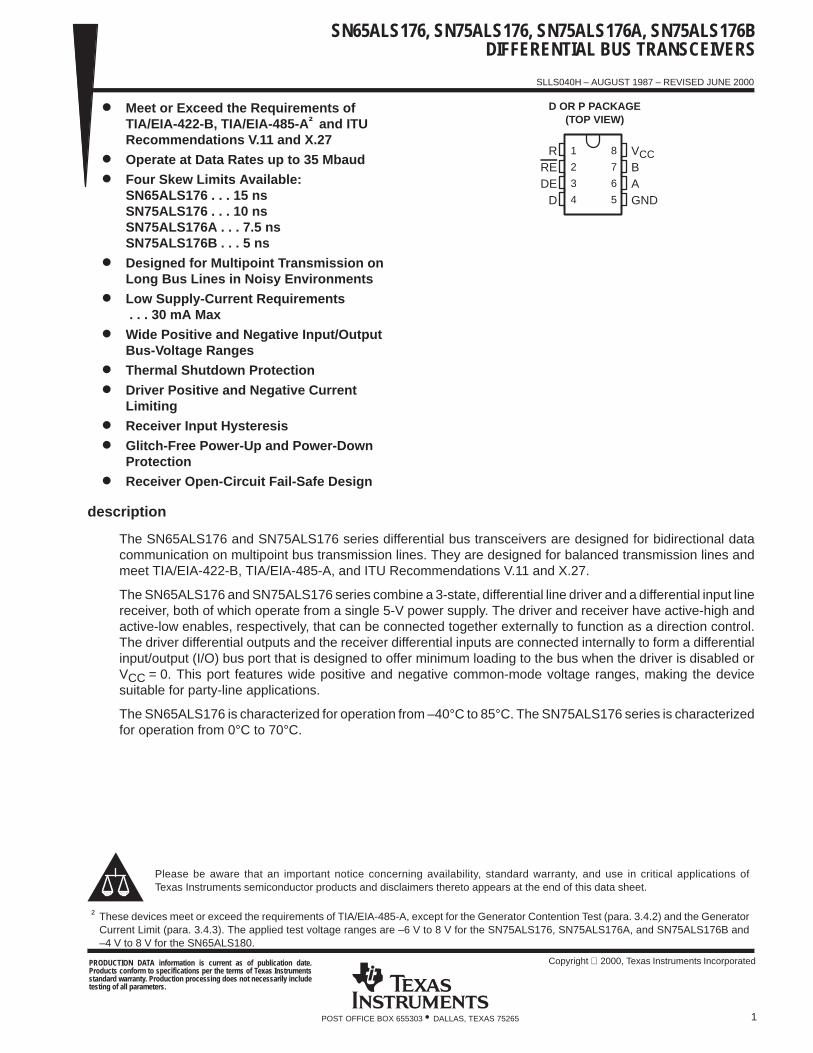
DRIVER SECTION
electrical characteristics over recommended ranges of supply voltage and operating free-airtemperature range (unless otherwise noted)
PARAMETER TEST CONDITIONS† MIN TYP‡ MAX UNIT
VIK Input clamp voltage II = –18 mA –1.5 V
VO Output voltage IO = 0 0 6 V
|VOD1| Differential output voltage IO = 0 1.5 6 V
|VOD2| Differential output voltageRL = 100 Ω, See Figure 1
1/2VOD1or 2§ V
OD2 g
RL = 54 Ω, See Figure 1 1.5 2.5 5 V
VOD3 Differential output voltage Vtest = –7 V to 12 V, See Figure 2 1.5 5 V
∆|VOD|Change in magnitude ofdifferential output voltage¶ RL = 54 Ω or 100 Ω, See Figure 1 ±0.2 V
VOC Common-mode output voltage RL = 54 Ω or 100 Ω, See Figure 13
–1V
∆|VOC|Change in magnitude ofcommon-mode output voltage¶ RL = 54 Ω or 100 Ω, See Figure 1 ±0.2 V
IO Output currentOutputs disabled VO = 12 V 1
mAIO Output current(see Note 4) VO = –7 V –0.8
mA
IIH High-level input current VI = 2.4 V 20 µA
IIL Low-level input current VI = 0.4 V –400 µA
#
VO = –4 V SN65ALS176 –250
#VO = –6 V SN75ALS176 –250
IOS Short-circuit output current# VO = 0 –150 mA
VO = VCC 250
VO = 8 V 250
ICC Supply current No loadOutputs enabled 23 30
mAICC Supply current No loadOutputs disabled 19 26
mA
† The power-off measurement in TIA/EIA-422-B applies to disabled outputs only and is not applied to combined inputs and outputs.‡ All typical values are at VCC = 5 V and TA = 25°C.§ The minimum VOD2 with a 100-Ω load is either 1/2 VOD1 or 2 V, whichever is greater.¶ ∆|VOD| and ∆|VOC| are the changes in magnitude of VOD and VOC, respectively, that occur when the input is changed from one logic state to the
other.# Duration of the short circuit should not exceed one second for this test.NOTE 4: This applies for power on and power off. Refer to TIA/EIA-485-A for exact conditions. The TIA/EIA-422-B limit does not apply for a
combined driver and receiver terminal.
SN65ALS176, SN75ALS176, SN75ALS176A, SN75ALS176BDIFFERENTIAL BUS TRANSCEIVERS
SLLS040H – AUGUST 1987 – REVISED JUNE 2000
6 POST OFFICE BOX 655303 • DALLAS, TEXAS 75265
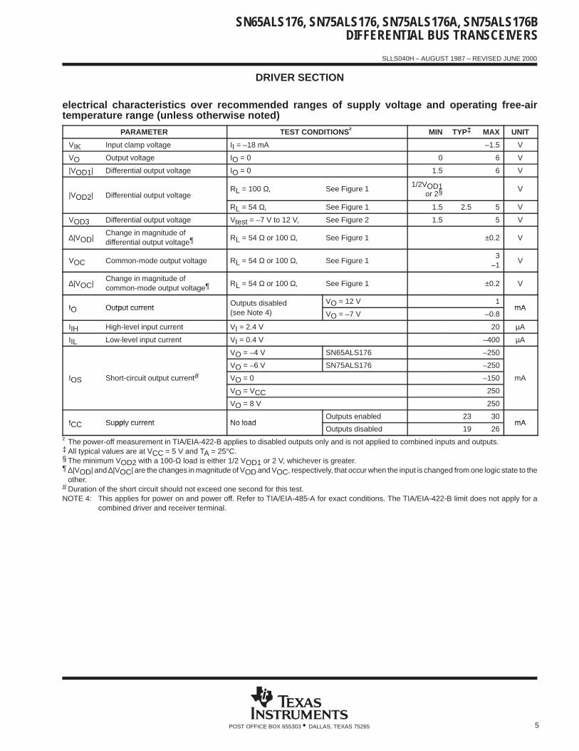
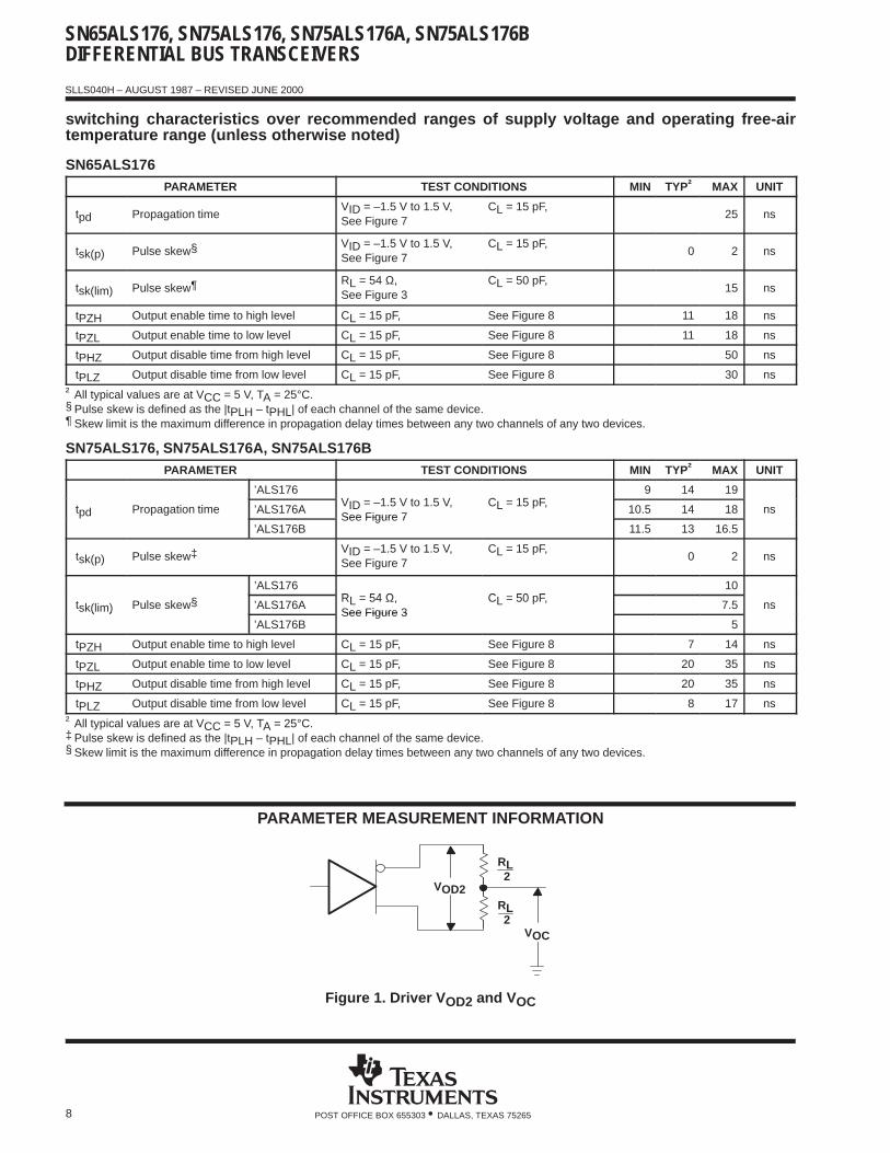
switching characteristics over recommended ranges of supply voltage and operating free-airtemperature range (unless otherwise noted)
SN65ALS176PARAMETER TEST CONDITIONS MIN TYP† MAX UNIT
td(OD) Differential output delay time RL = 54 Ω, CL = 50 pF, See Figure 3 15 ns
tsk(p) Pulse skew‡ RL = 54 Ω, CL = 50 pF, See Figure 3 0 2 ns
tsk(lim) Pulse skew§ RL = 54 Ω, CL = 50 pF, See Figure 3 15 ns
tt(OD) Differential output transition time RL = 54 Ω, CL = 50 pF, See Figure 3 8 ns
tPZH Output enable time to high level RL = 110 Ω, CL = 50 pF, See Figure 4 80 ns
tPZL Output enable time to low level RL = 110 Ω, CL = 50 pF, See Figure 5 30 ns
tPHZ Output disable time from high level RL = 110 Ω, CL = 50 pF, See Figure 4 50 ns
tPLZ Output disable time from low level RL = 110 Ω, CL = 50 pF, See Figure 5 30 ns
† All typical values are at VCC = 5 V, TA = 25°C.‡ Pulse skew is defined as the |tPLH – tPHL| of each channel of the same device.§ Skew limit is the maximum difference in propagation delay times between any two channels of any two devices.
SN75ALS176, SN75ALS176A, SN75ALS176BPARAMETER TEST CONDITIONS MIN TYP† MAX UNIT
Diff ti l t t’ALS176 3 8 13
td(OD)Differential outputdelay time
’ALS176A RL = 54 Ω, CL = 50 pF, See Figure 3 4 7 11.5 ns( ) delay time’ALS176B 5 8 10
tsk(p) Pulse skew‡ RL = 54 Ω, CL = 50 pF, See Figure 3 0 2 ns
§’ALS176 10
tsk(lim) Pulse skew§ ’ALS176A RL = 54 Ω, CL = 50 pF, See Figure 3 7.5 ns( )’ALS176B 5
tt(OD) Differential output transition time RL = 54 Ω, CL = 50 pF, See Figure 3 8 ns
tPZH Output enable time to high level RL = 110 Ω, CL = 50 pF, See Figure 4 23 50 ns
tPZL Output enable time to low level RL = 110 Ω, CL = 50 pF, See Figure 5 14 20 ns
tPHZ Output disable time from high level RL = 110 Ω, CL = 50 pF, See Figure 4 20 35 ns
tPLZ Output disable time from low level RL = 110 Ω, CL = 50 pF, See Figure 5 8 17 ns
† All typical values are at VCC = 5 V, TA = 25°C.‡ Pulse skew is defined as the |tPLH – tPHL| of each channel of the same device.§ Skew limit is the maximum difference in propagation delay times between any two channels of any two devices.
SYMBOL EQUIVALENTS
DATA-SHEETPARAMETER TIA/EIA-422-B TIA/EIA-485-A
VO Voa, Vob Voa, Vob
|VOD1| Vo Vo
|VOD2| Vt (RL = 100 Ω) Vt (RL = 54 Ω)
|VOD3| NoneVt (test terminationmeasurement 2)
∆|VOD| ||Vt| – |Vt|| ||Vt| – |Vt||
VOC |Vos| |Vos|
∆|VOC| |Vos – Vos| |Vos – Vos|
IOS |Isa|, |Isb| None
IO |Ixa|, |Ixb| Iia, Iib

SN65ALS176, SN75ALS176, SN75ALS176A, SN75ALS176BDIFFERENTIAL BUS TRANSCEIVERS
SLLS040H – AUGUST 1987 – REVISED JUNE 2000
7POST OFFICE BOX 655303 • DALLAS, TEXAS 75265
RECEIVER SECTION
electrical characteristics over recommended ranges of common-mode input voltage, supplyvoltage, and operating free-air temperature range (unless otherwise noted)
PARAMETER TEST CONDITIONS MIN TYP† MAX UNIT
VIT+ Positive-going input threshold voltage VO = 2.7 V, IO = –0.4 mA 0.2 V
VIT– Negative-going input threshold voltage VO = 0.5 V, IO = 8 mA –0.2‡ V
Vhys Hysteresis voltage (VIT+ – VIT–) 60 mV
VIK Enable-input clamp voltage II = –18 mA –1.5 V
VOH High level output voltageVID = 200 mV, IOH = –400 µA,
2 7 VVOH High-level output voltage ID ,See Figure 6
OH µ ,2.7 V
VOL Low-level output voltageVID = –200 mV,See Figure 6
IOL = 8 mA,0.45 V
IOZ High-impedance-state output current VO = 0.4 V to 2.4 V ±20 µA
VI Line input currentOther input = 0 V VI = 12 V 1
mAVI Line input current(see Note 5) VI = –7 V –0.8
mA
IIH High-level-enable input current VIH = 2.7 V 20 µA
IIL Low-level-enable input current VIL = 0.4 V –100 µA
rI Input resistance 12 20 kΩ
IOS Short-circuit output current VID = 200 mV, VO = 0 –15 –85 mA
ICC Supply current No loadOutputs enabled 23 30
mAICC Supply current No loadOutputs disabled 19 26
mA
† All typical values are at VCC = 5 V, TA = 25°C.‡ The algebraic convention, in which the less positive (more negative) limit is designated minimum, is used in this data sheet for common-mode
input voltage and threshold voltage levels only.NOTE 5: This applies for power on and power off. Refer to TIA/EIA-485-A for exact conditions.
SN65ALS176, SN75ALS176, SN75ALS176A, SN75ALS176BDIFFERENTIAL BUS TRANSCEIVERS
SLLS040H – AUGUST 1987 – REVISED JUNE 2000
8 POST OFFICE BOX 655303 • DALLAS, TEXAS 75265
switching characteristics over recommended ranges of supply voltage and operating free-airtemperature range (unless otherwise noted)
SN65ALS176PARAMETER TEST CONDITIONS MIN TYP† MAX UNIT
tpd Propagation timeVID = –1.5 V to 1.5 V,See Figure 7
CL = 15 pF,25 ns
tsk(p) Pulse skew§ VID = –1.5 V to 1.5 V,See Figure 7
CL = 15 pF,0 2 ns
tsk(lim) Pulse skew¶ RL = 54 Ω,See Figure 3
CL = 50 pF,15 ns
tPZH Output enable time to high level CL = 15 pF, See Figure 8 11 18 ns
tPZL Output enable time to low level CL = 15 pF, See Figure 8 11 18 ns
tPHZ Output disable time from high level CL = 15 pF, See Figure 8 50 ns
tPLZ Output disable time from low level CL = 15 pF, See Figure 8 30 ns
† All typical values are at VCC = 5 V, TA = 25°C.§ Pulse skew is defined as the |tPLH – tPHL| of each channel of the same device.¶ Skew limit is the maximum difference in propagation delay times between any two channels of any two devices.
SN75ALS176, SN75ALS176A, SN75ALS176BPARAMETER TEST CONDITIONS MIN TYP† MAX UNIT
’ALS176V 1 5 V t 1 5 V C 15 F
9 14 19
tpd Propagation time ’ALS176AVID = –1.5 V to 1.5 V,See Figure 7
CL = 15 pF,10.5 14 18 ns
’ALS176BSee Figure 7
11.5 13 16.5
tsk(p) Pulse skew‡ VID = –1.5 V to 1.5 V,See Figure 7
CL = 15 pF,0 2 ns
§’ALS176
R 54 Ω C 50 F10
tsk(lim) Pulse skew§ ’ALS176ARL = 54 Ω,See Figure 3
CL = 50 pF,7.5 ns( )
’ALS176BSee Figure 3
5
tPZH Output enable time to high level CL = 15 pF, See Figure 8 7 14 ns
tPZL Output enable time to low level CL = 15 pF, See Figure 8 20 35 ns
tPHZ Output disable time from high level CL = 15 pF, See Figure 8 20 35 ns
tPLZ Output disable time from low level CL = 15 pF, See Figure 8 8 17 ns
† All typical values are at VCC = 5 V, TA = 25°C.‡ Pulse skew is defined as the |tPLH – tPHL| of each channel of the same device.§ Skew limit is the maximum difference in propagation delay times between any two channels of any two devices.
PARAMETER MEASUREMENT INFORMATION
VOD2
VOC
RL 2
RL 2
Figure 1. Driver V OD2 and VOC

SN65ALS176, SN75ALS176, SN75ALS176A, SN75ALS176BDIFFERENTIAL BUS TRANSCEIVERS
SLLS040H – AUGUST 1987 – REVISED JUNE 2000
9POST OFFICE BOX 655303 • DALLAS, TEXAS 75265
PARAMETER MEASUREMENT INFORMATION
VOD3
Vtest
375 Ω
375 Ω
60 Ω
Figure 2. Driver V OD3
TEST CIRCUIT VOLTAGE WAVEFORMS
3 V
0 V
≈–2.5 V
50%10%
tt(OD) tt(OD)
td(ODL)(see Note C)
50%10%
90%90%
1.5 V
td(ODH)(see Note C)
Output
Input
Output
3 V
50 Ω
RL = 54 Ω≈2.5 VGenerator
(see Note B)
CL = 50 pF(see Note A)
1.5 V
NOTES: A. CL includes probe and jig capacitance.B. The input pulse is supplied by a generator having the following characteristics: PRR ≤ 1 MHz, 50% duty cycle, tr ≤ 6 ns, tf ≤ 6 ns,
ZO = 50 Ω.C. td(OD) = td(ODH) or td(ODL)
Figure 3. Driver Test Circuit and Voltage Waveforms
TEST CIRCUIT VOLTAGE WAVEFORMS
1.5 V
VOH
tPHZtPZH
0 V
3 V
1.5 V
2.3 VOutput
Input
Output
S1
0 V or 3 V
RL = 110 Ω
50 Ω
Voff ≈ 0
Generator(see Note B)
CL = 50 pF(see Note A)
NOTES: A. CL includes probe and jig capacitance.B. The input pulse is supplied by a generator having the following characteristics: PRR ≤ 1 MHz, 50% duty cycle, tr ≤ 6 ns, tf ≤ 6 ns,
ZO = 50 Ω.
Figure 4. Driver Test Circuit and Voltage Waveforms

SN65ALS176, SN75ALS176, SN75ALS176A, SN75ALS176BDIFFERENTIAL BUS TRANSCEIVERS
SLLS040H – AUGUST 1987 – REVISED JUNE 2000
10 POST OFFICE BOX 655303 • DALLAS, TEXAS 75265
PARAMETER MEASUREMENT INFORMATION
TEST CIRCUIT VOLTAGE WAVEFORMS
VOL
tPLZtPZL
5 V
0.5 V2.3 V
0 V
3 V
1.5 V1.5 V
5 V
Output
InputOutputS1
0 V or 3 V
50 Ω
RL = 110 Ω
Generator(see Note B)
CL = 50 pF(see Note A)
NOTES: A. CL includes probe and jig capacitance.B. The input pulse is supplied by a generator having the following characteristics: PRR ≤ 1 MHz, 50% duty cycle, tr ≤ 6 ns, tf ≤ 6 ns,
ZO = 50 Ω.
Figure 5. Driver Test Circuit and Voltage Waveforms
–IOH
VOH
+ IOLVOL
VID
Figure 6. Receiver V OH and VOL Test Circuit
TEST CIRCUIT VOLTAGE WAVEFORMS
VOL
VOH
3 V
0 V
tPHL(see Note C)
tPLH(see Note C)
Output
Input 1.5 V
1.3 V
51 Ω Output
0 V
1.5 V
Generator(see Note B)
CL = 15 pF(see Note A)
1.5 V
1.3 V
NOTES: A. CL includes probe and jig capacitance.B. The input pulse is supplied by a generator having the following characteristics: PRR ≤ 1 MHz, 50% duty cycle, tr ≤ 6 ns, tf ≤ 6 ns,
ZO = 50 Ω.C. tpd = tPLH or tPHL
Figure 7. Receiver Test Circuit and Voltage Waveforms

SN65ALS176, SN75ALS176, SN75ALS176A, SN75ALS176BDIFFERENTIAL BUS TRANSCEIVERS
SLLS040H – AUGUST 1987 – REVISED JUNE 2000
11POST OFFICE BOX 655303 • DALLAS, TEXAS 75265
PARAMETER MEASUREMENT INFORMATION
TEST CIRCUIT
VOLTAGE WAVEFORMS
2 kΩ
5 V
S3
1N916 or Equivalent5 kΩ
50 Ω
S11.5 V
– 1.5 V
tPZL
1.5 V
1.5 V
3 V
0 V
VOL
tPZH
1.5 V
1.5 V
S1 to 1.5 VS2 OpenS3 Closed
Input
0 V
3 V
Output
0 V
VOH
VOL
0.5 V
1.5 V
0 V
3 V
tPLZ
VOH
tPHZ
3 V
0 V
0.5 V
Input
Output
≈1.3 V
Input
Output
Input
Output
≈4.5 V
≈1.3 V
CL = 15 pF(see Note A)
Generator(see Note B)
1.5 V
NOTES: A. CL includes probe and jig capacitance.B. The input pulse is supplied by a generator having the following characteristics: PRR ≤ 1 MHz, 50% duty cycle, tr ≤ 6 ns, tf ≤ 6 ns,
ZO = 50 Ω.
Output
S2
S1 to 1.5 VS2 ClosedS3 Closed
S1 to –1.5 VS2 ClosedS3 Open
S1 to –1.5 VS2 ClosedS3 Closed
Figure 8. Receiver Test Circuit and Voltage Waveforms

SN65ALS176, SN75ALS176, SN75ALS176A, SN75ALS176BDIFFERENTIAL BUS TRANSCEIVERS
SLLS040H – AUGUST 1987 – REVISED JUNE 2000
12 POST OFFICE BOX 655303 • DALLAS, TEXAS 75265
TYPICAL CHARACTERISTICS †
Figure 9
2.5
1.5
1
00 –20 –40 –60
– H
igh-
Leve
l Out
put V
olta
ge –
V
3.5
4
DRIVERHIGH-LEVEL OUTPUT VOLTAGE
vsHIGH-LEVEL OUTPUT CURRENT
5
–80 –100 –120
V OH
IOH – High-Level Output Current – mA
4.5
3
2
0.5
VCC = 5 VTA = 25°C
Figure 10
2.5
1.5
1
00 20 40 60
– Lo
w-L
evel
Out
put V
olta
ge –
V
3.5
4
DRIVERLOW-LEVEL OUTPUT VOLTAGE
vsLOW-LEVEL OUTPUT CURRENT
5
80 100 120
V OL
IOL – Low-Level Output Current – mA
4.5
3
2
0.5
VCC = 5 VTA = 25°C
2
1.5
0.5
00 10 20 30 40 50 60
– D
iffer
entia
l Out
put V
olta
ge –
V
2.5
3.5
DRIVERDIFFERENTIAL OUTPUT VOLTAGE
vsOUTPUT CURRENT
4
70 80 90 100
1
3
VCC = 5 VTA = 25°C
V OD
IO – Output Current – mA
Figure 11
† Operation of the device at these or any other conditions beyond those indicated under ‘‘recommended operating conditions” is not implied.
SN65ALS176, SN75ALS176, SN75ALS176A, SN75ALS176BDIFFERENTIAL BUS TRANSCEIVERS
SLLS040H – AUGUST 1987 – REVISED JUNE 2000
13POST OFFICE BOX 655303 • DALLAS, TEXAS 75265
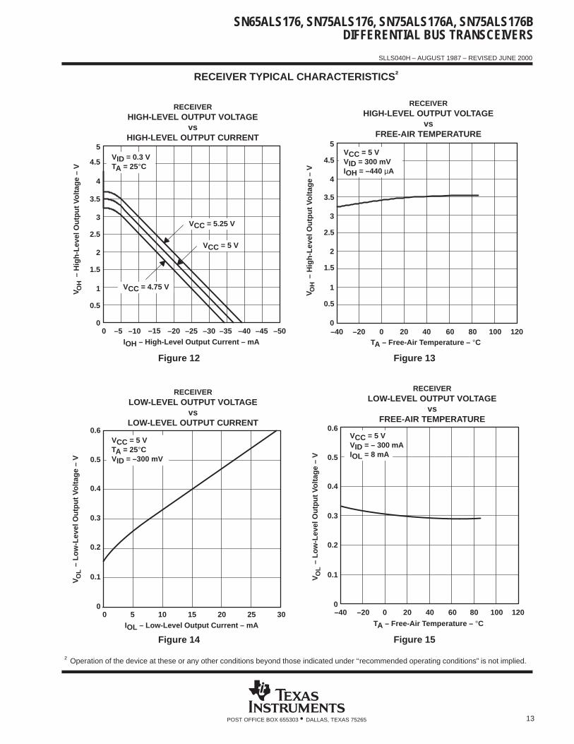
RECEIVER TYPICAL CHARACTERISTICS †
Figure 12
2
1
00 –10 –20 –30
– H
igh-
Leve
l Out
put V
olta
ge –
V
3
4
RECEIVERHIGH-LEVEL OUTPUT VOLTAGE
vsHIGH-LEVEL OUTPUT CURRENT
5
–40 –50
VCC = 5.25 V
VCC = 5 V
IOH – High-Level Output Current – mA
V OH
VID = 0.3 VTA = 25°C4.5
3.5
2.5
1.5
0.5
–5 –15 –25 –35 –45
VCC = 4.75 V
Figure 13
2
0–40 –20 0 20 40 60 80
RECEIVERHIGH-LEVEL OUTPUT VOLTAGE
vsFREE-AIR TEMPERATURE
5
100 120
4
3
1
– H
igh-
Leve
l Out
put V
olta
ge –
VV O
H
TA – Free-Air Temperature – °C
VCC = 5 VVID = 300 mVIOH = –440 µA
4.5
3.5
2.5
1.5
0.5
0.3
0.2
0.1
00 5 10
– Lo
w-L
evel
Out
put V
olta
ge –
V
0.4
0.5
RECEIVERLOW-LEVEL OUTPUT VOLTAGE
vsLOW-LEVEL OUTPUT CURRENT
0.6
15 20 25 30IOL – Low-Level Output Current – mA
VO
L
VCC = 5 VTA = 25°CVID = –300 mV
Figure 14 Figure 15
0.3
0.2
0.1
0–40 –20 0 20 40 60
0.4
0.5
RECEIVERLOW-LEVEL OUTPUT VOLTAGE
vsFREE-AIR TEMPERATURE
0.6
80 100 120
– Lo
w-L
evel
Out
put V
olta
ge –
VV
OL
TA – Free-Air Temperature – °C
VCC = 5 VVID = – 300 mAIOL = 8 mA
† Operation of the device at these or any other conditions beyond those indicated under ‘‘recommended operating conditions” is not implied.

SN65ALS176, SN75ALS176, SN75ALS176A, SN75ALS176BDIFFERENTIAL BUS TRANSCEIVERS
SLLS040H – AUGUST 1987 – REVISED JUNE 2000
14 POST OFFICE BOX 655303 • DALLAS, TEXAS 75265
TYPICAL CHARACTERISTICS †
Figure 16
2
1
00 0.5 1 1.5
– O
utpu
t Vol
tage
– V
3
4
RECEIVEROUTPUT VOLTAGE
vsENABLE VOLTAGE
5
2 2.5 3
VCC = 5 VVCC = 4.75 V
VID = 0.3 VLoad = 8 k Ω to GNDTA = 25°C
VI(en) – Enable Voltage – V
VO
VCC = 5.25 V
3
2
1
00 0.5 1
4
5
RECEIVEROUTPUT VOLTAGE
vsENABLE VOLTAGE
6
1.5 2 2.5 3
VID = 0.3 VLoad = 1 k Ω to VCCTA = 25°C
VCC = 5.25 V
VCC = 5 V
VCC = 4.75 V
VI(en) – Enable Voltage – V
– O
utpu
t Vol
tage
– V
VO
Figure 17
APPLICATION INFORMATION
Up to53 Transceivers
NOTE A: The line should terminate at both ends in its characteristic impedance (RT = ZO). Stub lengths off the main line should be kept as shortas possible.
RT RT
Figure 18. Typical Application Circuit
† Operation of the device at these or any other conditions beyond those indicated under ‘‘recommended operating conditions” is not implied.

IMPORTANT NOTICE
Texas Instruments Incorporated and its subsidiaries (TI) reserve the right to make corrections, modifications, enhancements,improvements, and other changes to its products and services at any time and to discontinue any product or service without notice.Customers should obtain the latest relevant information before placing orders and should verify that such information is current andcomplete. All products are sold subject to TI’s terms and conditions of sale supplied at the time of order acknowledgment.
TI warrants performance of its hardware products to the specifications applicable at the time of sale in accordance with TI’sstandard warranty. Testing and other quality control techniques are used to the extent TI deems necessary to support thiswarranty. Except where mandated by government requirements, testing of all parameters of each product is not necessarilyperformed.
TI assumes no liability for applications assistance or customer product design. Customers are responsible for their products andapplications using TI components. To minimize the risks associated with customer products and applications, customers shouldprovide adequate design and operating safeguards.
TI does not warrant or represent that any license, either express or implied, is granted under any TI patent right, copyright, maskwork right, or other TI intellectual property right relating to any combination, machine, or process in which TI products or servicesare used. Information published by TI regarding third-party products or services does not constitute a license from TI to use suchproducts or services or a warranty or endorsement thereof. Use of such information may require a license from a third party underthe patents or other intellectual property of the third party, or a license from TI under the patents or other intellectual property of TI.
Reproduction of information in TI data books or data sheets is permissible only if reproduction is without alteration and isaccompanied by all associated warranties, conditions, limitations, and notices. Reproduction of this information with alteration is anunfair and deceptive business practice. TI is not responsible or liable for such altered documentation.
Resale of TI products or services with statements different from or beyond the parameters stated by TI for that product or servicevoids all express and any implied warranties for the associated TI product or service and is an unfair and deceptive businesspractice. TI is not responsible or liable for any such statements.
TI products are not authorized for use in safety-critical applications (such as life support) where a failure of the TI product wouldreasonably be expected to cause severe personal injury or death, unless officers of the parties have executed an agreementspecifically governing such use. Buyers represent that they have all necessary expertise in the safety and regulatory ramificationsof their applications, and acknowledge and agree that they are solely responsible for all legal, regulatory and safety-relatedrequirements concerning their products and any use of TI products in such safety-critical applications, notwithstanding anyapplications-related information or support that may be provided by TI. Further, Buyers must fully indemnify TI and itsrepresentatives against any damages arising out of the use of TI products in such safety-critical applications.
TI products are neither designed nor intended for use in military/aerospace applications or environments unless the TI products arespecifically designated by TI as military-grade or "enhanced plastic." Only products designated by TI as military-grade meet militaryspecifications. Buyers acknowledge and agree that any such use of TI products which TI has not designated as military-grade issolely at the Buyer's risk, and that they are solely responsible for compliance with all legal and regulatory requirements inconnection with such use.
TI products are neither designed nor intended for use in automotive applications or environments unless the specific TI productsare designated by TI as compliant with ISO/TS 16949 requirements. Buyers acknowledge and agree that, if they use anynon-designated products in automotive applications, TI will not be responsible for any failure to meet such requirements.
Following are URLs where you can obtain information on other Texas Instruments products and application solutions:
Products Applications
Amplifiers amplifier.ti.com Audio www.ti.com/audio
Data Converters dataconverter.ti.com Automotive www.ti.com/automotive
DSP dsp.ti.com Broadband www.ti.com/broadband
Interface interface.ti.com Digital Control www.ti.com/digitalcontrol
Logic logic.ti.com Military www.ti.com/military
Power Mgmt power.ti.com Optical Networking www.ti.com/opticalnetwork
Microcontrollers microcontroller.ti.com Security www.ti.com/security
Low Power www.ti.com/lpw Telephony www.ti.com/telephonyWireless
Video & Imaging www.ti.com/video
Wireless www.ti.com/wireless
Mailing Address: Texas Instruments, Post Office Box 655303, Dallas, Texas 75265Copyright © 2007, Texas Instruments Incorporated

PACKAGING INFORMATION
Orderable Device Status (1) PackageType
PackageDrawing
Pins PackageQty
Eco Plan (2) Lead/Ball Finish MSL Peak Temp (3)
SN65ALS176D ACTIVE SOIC D 8 75 Green (RoHS &no Sb/Br)
CU NIPDAU Level-1-260C-UNLIM
SN65ALS176DE4 ACTIVE SOIC D 8 75 Green (RoHS &no Sb/Br)
CU NIPDAU Level-1-260C-UNLIM
SN65ALS176DG4 ACTIVE SOIC D 8 75 Green (RoHS &no Sb/Br)
CU NIPDAU Level-1-260C-UNLIM
SN65ALS176DR ACTIVE SOIC D 8 2500 Green (RoHS &no Sb/Br)
CU NIPDAU Level-1-260C-UNLIM
SN65ALS176DRE4 ACTIVE SOIC D 8 2500 Green (RoHS &no Sb/Br)
CU NIPDAU Level-1-260C-UNLIM
SN65ALS176DRG4 ACTIVE SOIC D 8 2500 Green (RoHS &no Sb/Br)
CU NIPDAU Level-1-260C-UNLIM
SN65ALS176P OBSOLETE PDIP P 8 TBD Call TI Call TI
SN75ALS176AD ACTIVE SOIC D 8 75 Green (RoHS &no Sb/Br)
CU NIPDAU Level-1-260C-UNLIM
SN75ALS176ADE4 ACTIVE SOIC D 8 75 Green (RoHS &no Sb/Br)
CU NIPDAU Level-1-260C-UNLIM
SN75ALS176ADG4 ACTIVE SOIC D 8 75 Green (RoHS &no Sb/Br)
CU NIPDAU Level-1-260C-UNLIM
SN75ALS176ADR ACTIVE SOIC D 8 2500 Green (RoHS &no Sb/Br)
CU NIPDAU Level-1-260C-UNLIM
SN75ALS176ADRE4 ACTIVE SOIC D 8 2500 Green (RoHS &no Sb/Br)
CU NIPDAU Level-1-260C-UNLIM
SN75ALS176ADRG4 ACTIVE SOIC D 8 2500 Green (RoHS &no Sb/Br)
CU NIPDAU Level-1-260C-UNLIM
SN75ALS176AP ACTIVE PDIP P 8 50 Pb-Free(RoHS)
CU NIPDAU N / A for Pkg Type
SN75ALS176APE4 ACTIVE PDIP P 8 50 Pb-Free(RoHS)
CU NIPDAU N / A for Pkg Type
SN75ALS176BD ACTIVE SOIC D 8 75 Green (RoHS &no Sb/Br)
CU NIPDAU Level-1-260C-UNLIM
SN75ALS176BDE4 ACTIVE SOIC D 8 75 Green (RoHS &no Sb/Br)
CU NIPDAU Level-1-260C-UNLIM
SN75ALS176BDG4 ACTIVE SOIC D 8 75 Green (RoHS &no Sb/Br)
CU NIPDAU Level-1-260C-UNLIM
SN75ALS176BDR ACTIVE SOIC D 8 2500 Green (RoHS &no Sb/Br)
CU NIPDAU Level-1-260C-UNLIM
SN75ALS176BDRE4 ACTIVE SOIC D 8 2500 Green (RoHS &no Sb/Br)
CU NIPDAU Level-1-260C-UNLIM
SN75ALS176BDRG4 ACTIVE SOIC D 8 2500 Green (RoHS &no Sb/Br)
CU NIPDAU Level-1-260C-UNLIM
SN75ALS176BP ACTIVE PDIP P 8 50 Pb-Free(RoHS)
CU NIPDAU N / A for Pkg Type
SN75ALS176BPE4 ACTIVE PDIP P 8 50 Pb-Free(RoHS)
CU NIPDAU N / A for Pkg Type
SN75ALS176D ACTIVE SOIC D 8 75 Green (RoHS &no Sb/Br)
CU NIPDAU Level-1-260C-UNLIM
SN75ALS176DE4 ACTIVE SOIC D 8 75 Green (RoHS &no Sb/Br)
CU NIPDAU Level-1-260C-UNLIM
PACKAGE OPTION ADDENDUM
www.ti.com 23-Apr-2007
Addendum-Page 1

Orderable Device Status (1) PackageType
PackageDrawing
Pins PackageQty
Eco Plan (2) Lead/Ball Finish MSL Peak Temp (3)
SN75ALS176DG4 ACTIVE SOIC D 8 75 Green (RoHS &no Sb/Br)
CU NIPDAU Level-1-260C-UNLIM
SN75ALS176DR ACTIVE SOIC D 8 2500 Green (RoHS &no Sb/Br)
CU NIPDAU Level-1-260C-UNLIM
SN75ALS176DRE4 ACTIVE SOIC D 8 2500 Green (RoHS &no Sb/Br)
CU NIPDAU Level-1-260C-UNLIM
SN75ALS176DRG4 ACTIVE SOIC D 8 2500 Green (RoHS &no Sb/Br)
CU NIPDAU Level-1-260C-UNLIM
SN75ALS176P ACTIVE PDIP P 8 50 Pb-Free(RoHS)
CU NIPDAU N / A for Pkg Type
SN75ALS176PE4 ACTIVE PDIP P 8 50 Pb-Free(RoHS)
CU NIPDAU N / A for Pkg Type
(1) The marketing status values are defined as follows:ACTIVE: Product device recommended for new designs.LIFEBUY: TI has announced that the device will be discontinued, and a lifetime-buy period is in effect.NRND: Not recommended for new designs. Device is in production to support existing customers, but TI does not recommend using this part ina new design.PREVIEW: Device has been announced but is not in production. Samples may or may not be available.OBSOLETE: TI has discontinued the production of the device.
(2) Eco Plan - The planned eco-friendly classification: Pb-Free (RoHS), Pb-Free (RoHS Exempt), or Green (RoHS & no Sb/Br) - please checkhttp://www.ti.com/productcontent for the latest availability information and additional product content details.TBD: The Pb-Free/Green conversion plan has not been defined.Pb-Free (RoHS): TI's terms "Lead-Free" or "Pb-Free" mean semiconductor products that are compatible with the current RoHS requirementsfor all 6 substances, including the requirement that lead not exceed 0.1% by weight in homogeneous materials. Where designed to be solderedat high temperatures, TI Pb-Free products are suitable for use in specified lead-free processes.Pb-Free (RoHS Exempt): This component has a RoHS exemption for either 1) lead-based flip-chip solder bumps used between the die andpackage, or 2) lead-based die adhesive used between the die and leadframe. The component is otherwise considered Pb-Free (RoHScompatible) as defined above.Green (RoHS & no Sb/Br): TI defines "Green" to mean Pb-Free (RoHS compatible), and free of Bromine (Br) and Antimony (Sb) based flameretardants (Br or Sb do not exceed 0.1% by weight in homogeneous material)
(3) MSL, Peak Temp. -- The Moisture Sensitivity Level rating according to the JEDEC industry standard classifications, and peak soldertemperature.
Important Information and Disclaimer:The information provided on this page represents TI's knowledge and belief as of the date that it isprovided. TI bases its knowledge and belief on information provided by third parties, and makes no representation or warranty as to theaccuracy of such information. Efforts are underway to better integrate information from third parties. TI has taken and continues to takereasonable steps to provide representative and accurate information but may not have conducted destructive testing or chemical analysis onincoming materials and chemicals. TI and TI suppliers consider certain information to be proprietary, and thus CAS numbers and other limitedinformation may not be available for release.
In no event shall TI's liability arising out of such information exceed the total purchase price of the TI part(s) at issue in this document sold by TIto Customer on an annual basis.
PACKAGE OPTION ADDENDUM
www.ti.com 23-Apr-2007
Addendum-Page 2

TAPE AND REEL INFORMATION
*All dimensions are nominal
Device PackageType
PackageDrawing
Pins SPQ ReelDiameter
(mm)
ReelWidth
W1 (mm)
A0 (mm) B0 (mm) K0 (mm) P1(mm)
W(mm)
Pin1Quadrant
SN65ALS176DR SOIC D 8 2500 330.0 12.4 6.4 5.2 2.1 8.0 12.0 Q1
SN75ALS176ADR SOIC D 8 2500 330.0 12.4 6.4 5.2 2.1 8.0 12.0 Q1
SN75ALS176BDR SOIC D 8 2500 330.0 12.4 6.4 5.2 2.1 8.0 12.0 Q1
SN75ALS176DR SOIC D 8 2500 330.0 12.4 6.4 5.2 2.1 8.0 12.0 Q1
PACKAGE MATERIALS INFORMATION
www.ti.com 19-Mar-2008
Pack Materials-Page 1
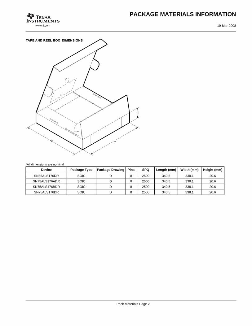
*All dimensions are nominal
Device Package Type Package Drawing Pins SPQ Length (mm) Width (mm) Height (mm)
SN65ALS176DR SOIC D 8 2500 340.5 338.1 20.6
SN75ALS176ADR SOIC D 8 2500 340.5 338.1 20.6
SN75ALS176BDR SOIC D 8 2500 340.5 338.1 20.6
SN75ALS176DR SOIC D 8 2500 340.5 338.1 20.6
PACKAGE MATERIALS INFORMATION
www.ti.com 19-Mar-2008
Pack Materials-Page 2


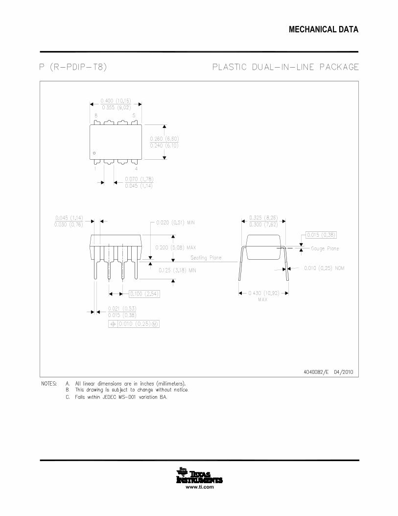
MECHANICAL DATA
MPDI001A – JANUARY 1995 – REVISED JUNE 1999
POST OFFICE BOX 655303 • DALLAS, TEXAS 75265
P (R-PDIP-T8) PLASTIC DUAL-IN-LINE
8
4
0.015 (0,38)
Gage Plane
0.325 (8,26)0.300 (7,62)
0.010 (0,25) NOM
MAX0.430 (10,92)
4040082/D 05/98
0.200 (5,08) MAX
0.125 (3,18) MIN
5
0.355 (9,02)
0.020 (0,51) MIN
0.070 (1,78) MAX
0.240 (6,10)0.260 (6,60)
0.400 (10,60)
1
0.015 (0,38)0.021 (0,53)
Seating Plane
M0.010 (0,25)
0.100 (2,54)
NOTES: A. All linear dimensions are in inches (millimeters).B. This drawing is subject to change without notice.C. Falls within JEDEC MS-001
For the latest package information, go to http://www.ti.com/sc/docs/package/pkg_info.htm

PACKAGE OPTION ADDENDUM
www.ti.com 17-Mar-2017
Addendum-Page 1
PACKAGING INFORMATION
Orderable Device Status(1)
Package Type PackageDrawing
Pins PackageQty
Eco Plan(2)
Lead/Ball Finish(6)
MSL Peak Temp(3)
Op Temp (°C) Device Marking(4/5)
Samples
SN65ALS176D ACTIVE SOIC D 8 75 Green (RoHS& no Sb/Br)
CU NIPDAU Level-1-260C-UNLIM -40 to 85 65A176
SN65ALS176DG4 ACTIVE SOIC D 8 75 Green (RoHS& no Sb/Br)
CU NIPDAU Level-1-260C-UNLIM -40 to 85 65A176
SN65ALS176DR ACTIVE SOIC D 8 2500 Green (RoHS& no Sb/Br)
CU NIPDAU Level-1-260C-UNLIM -40 to 85 65A176
SN65ALS176DRG4 ACTIVE SOIC D 8 2500 Green (RoHS& no Sb/Br)
CU NIPDAU Level-1-260C-UNLIM -40 to 85 65A176
SN75ALS176AD ACTIVE SOIC D 8 75 Green (RoHS& no Sb/Br)
CU NIPDAU Level-1-260C-UNLIM 0 to 70 7A176A
SN75ALS176ADG4 ACTIVE SOIC D 8 75 Green (RoHS& no Sb/Br)
CU NIPDAU Level-1-260C-UNLIM 0 to 70 7A176A
SN75ALS176ADR ACTIVE SOIC D 8 2500 Green (RoHS& no Sb/Br)
CU NIPDAU Level-1-260C-UNLIM 0 to 70 7A176A
SN75ALS176ADRE4 ACTIVE SOIC D 8 2500 Green (RoHS& no Sb/Br)
CU NIPDAU Level-1-260C-UNLIM 0 to 70 7A176A
SN75ALS176ADRG4 ACTIVE SOIC D 8 2500 Green (RoHS& no Sb/Br)
CU NIPDAU Level-1-260C-UNLIM 0 to 70 7A176A
SN75ALS176AP ACTIVE PDIP P 8 50 Pb-Free(RoHS)
CU NIPDAU N / A for Pkg Type 0 to 70 75ALS176A
SN75ALS176BD ACTIVE SOIC D 8 75 Green (RoHS& no Sb/Br)
CU NIPDAU Level-1-260C-UNLIM 0 to 70 7A176B
SN75ALS176BDG4 ACTIVE SOIC D 8 75 Green (RoHS& no Sb/Br)
CU NIPDAU Level-1-260C-UNLIM 0 to 70 7A176B
SN75ALS176BDR ACTIVE SOIC D 8 2500 Green (RoHS& no Sb/Br)
CU NIPDAU Level-1-260C-UNLIM 0 to 70 7A176B
SN75ALS176BDRE4 ACTIVE SOIC D 8 2500 Green (RoHS& no Sb/Br)
CU NIPDAU Level-1-260C-UNLIM 0 to 70 7A176B
SN75ALS176BDRG4 ACTIVE SOIC D 8 2500 Green (RoHS& no Sb/Br)
CU NIPDAU Level-1-260C-UNLIM 0 to 70 7A176B
SN75ALS176BP ACTIVE PDIP P 8 50 Pb-Free(RoHS)
CU NIPDAU N / A for Pkg Type 0 to 70 75ALS176B
SN75ALS176D ACTIVE SOIC D 8 75 Green (RoHS& no Sb/Br)
CU NIPDAU Level-1-260C-UNLIM 0 to 70 75A176

PACKAGE OPTION ADDENDUM
www.ti.com 17-Mar-2017
Addendum-Page 2
Orderable Device Status(1)
Package Type PackageDrawing
Pins PackageQty
Eco Plan(2)
Lead/Ball Finish(6)
MSL Peak Temp(3)
Op Temp (°C) Device Marking(4/5)
Samples
SN75ALS176DR ACTIVE SOIC D 8 2500 Green (RoHS& no Sb/Br)
CU NIPDAU Level-1-260C-UNLIM 0 to 70 75A176
SN75ALS176P ACTIVE PDIP P 8 50 Pb-Free(RoHS)
CU NIPDAU N / A for Pkg Type 0 to 70 75ALS176
SN75ALS176PE4 ACTIVE PDIP P 8 50 Pb-Free(RoHS)
CU NIPDAU N / A for Pkg Type 0 to 70 75ALS176
(1) The marketing status values are defined as follows:ACTIVE: Product device recommended for new designs.LIFEBUY: TI has announced that the device will be discontinued, and a lifetime-buy period is in effect.NRND: Not recommended for new designs. Device is in production to support existing customers, but TI does not recommend using this part in a new design.PREVIEW: Device has been announced but is not in production. Samples may or may not be available.OBSOLETE: TI has discontinued the production of the device.
(2) Eco Plan - The planned eco-friendly classification: Pb-Free (RoHS), Pb-Free (RoHS Exempt), or Green (RoHS & no Sb/Br) - please check http://www.ti.com/productcontent for the latest availabilityinformation and additional product content details.TBD: The Pb-Free/Green conversion plan has not been defined.Pb-Free (RoHS): TI's terms "Lead-Free" or "Pb-Free" mean semiconductor products that are compatible with the current RoHS requirements for all 6 substances, including the requirement thatlead not exceed 0.1% by weight in homogeneous materials. Where designed to be soldered at high temperatures, TI Pb-Free products are suitable for use in specified lead-free processes.Pb-Free (RoHS Exempt): This component has a RoHS exemption for either 1) lead-based flip-chip solder bumps used between the die and package, or 2) lead-based die adhesive used betweenthe die and leadframe. The component is otherwise considered Pb-Free (RoHS compatible) as defined above.Green (RoHS & no Sb/Br): TI defines "Green" to mean Pb-Free (RoHS compatible), and free of Bromine (Br) and Antimony (Sb) based flame retardants (Br or Sb do not exceed 0.1% by weightin homogeneous material)
(3) MSL, Peak Temp. - The Moisture Sensitivity Level rating according to the JEDEC industry standard classifications, and peak solder temperature.
(4) There may be additional marking, which relates to the logo, the lot trace code information, or the environmental category on the device.
(5) Multiple Device Markings will be inside parentheses. Only one Device Marking contained in parentheses and separated by a "~" will appear on a device. If a line is indented then it is a continuationof the previous line and the two combined represent the entire Device Marking for that device.
(6) Lead/Ball Finish - Orderable Devices may have multiple material finish options. Finish options are separated by a vertical ruled line. Lead/Ball Finish values may wrap to two lines if the finishvalue exceeds the maximum column width.
Important Information and Disclaimer:The information provided on this page represents TI's knowledge and belief as of the date that it is provided. TI bases its knowledge and belief on informationprovided by third parties, and makes no representation or warranty as to the accuracy of such information. Efforts are underway to better integrate information from third parties. TI has taken andcontinues to take reasonable steps to provide representative and accurate information but may not have conducted destructive testing or chemical analysis on incoming materials and chemicals.TI and TI suppliers consider certain information to be proprietary, and thus CAS numbers and other limited information may not be available for release.

PACKAGE OPTION ADDENDUM
www.ti.com 17-Mar-2017
Addendum-Page 3
In no event shall TI's liability arising out of such information exceed the total purchase price of the TI part(s) at issue in this document sold by TI to Customer on an annual basis.

TAPE AND REEL INFORMATION
*All dimensions are nominal
Device PackageType
PackageDrawing
Pins SPQ ReelDiameter
(mm)
ReelWidth
W1 (mm)
A0 (mm) B0 (mm) K0 (mm) P1(mm)
W(mm)
Pin1Quadrant
SN65ALS176DR SOIC D 8 2500 330.0 12.4 6.4 5.2 2.1 8.0 12.0 Q1
SN75ALS176ADR SOIC D 8 2500 330.0 12.4 6.4 5.2 2.1 8.0 12.0 Q1
SN75ALS176BDR SOIC D 8 2500 330.0 12.4 6.4 5.2 2.1 8.0 12.0 Q1
SN75ALS176DR SOIC D 8 2500 330.0 12.4 6.4 5.2 2.1 8.0 12.0 Q1
PACKAGE MATERIALS INFORMATION
www.ti.com 19-Mar-2008
Pack Materials-Page 1

*All dimensions are nominal
Device Package Type Package Drawing Pins SPQ Length (mm) Width (mm) Height (mm)
SN65ALS176DR SOIC D 8 2500 340.5 338.1 20.6
SN75ALS176ADR SOIC D 8 2500 340.5 338.1 20.6
SN75ALS176BDR SOIC D 8 2500 340.5 338.1 20.6
SN75ALS176DR SOIC D 8 2500 340.5 338.1 20.6
PACKAGE MATERIALS INFORMATION
www.ti.com 19-Mar-2008
Pack Materials-Page 2


IMPORTANT NOTICE
Texas Instruments Incorporated (TI) reserves the right to make corrections, enhancements, improvements and other changes to itssemiconductor products and services per JESD46, latest issue, and to discontinue any product or service per JESD48, latest issue. Buyersshould obtain the latest relevant information before placing orders and should verify that such information is current and complete.TI’s published terms of sale for semiconductor products (http://www.ti.com/sc/docs/stdterms.htm) apply to the sale of packaged integratedcircuit products that TI has qualified and released to market. Additional terms may apply to the use or sale of other types of TI products andservices.Reproduction of significant portions of TI information in TI data sheets is permissible only if reproduction is without alteration and isaccompanied by all associated warranties, conditions, limitations, and notices. TI is not responsible or liable for such reproduceddocumentation. Information of third parties may be subject to additional restrictions. Resale of TI products or services with statementsdifferent from or beyond the parameters stated by TI for that product or service voids all express and any implied warranties for theassociated TI product or service and is an unfair and deceptive business practice. TI is not responsible or liable for any such statements.Buyers and others who are developing systems that incorporate TI products (collectively, “Designers”) understand and agree that Designersremain responsible for using their independent analysis, evaluation and judgment in designing their applications and that Designers havefull and exclusive responsibility to assure the safety of Designers' applications and compliance of their applications (and of all TI productsused in or for Designers’ applications) with all applicable regulations, laws and other applicable requirements. Designer represents that, withrespect to their applications, Designer has all the necessary expertise to create and implement safeguards that (1) anticipate dangerousconsequences of failures, (2) monitor failures and their consequences, and (3) lessen the likelihood of failures that might cause harm andtake appropriate actions. Designer agrees that prior to using or distributing any applications that include TI products, Designer willthoroughly test such applications and the functionality of such TI products as used in such applications.TI’s provision of technical, application or other design advice, quality characterization, reliability data or other services or information,including, but not limited to, reference designs and materials relating to evaluation modules, (collectively, “TI Resources”) are intended toassist designers who are developing applications that incorporate TI products; by downloading, accessing or using TI Resources in anyway, Designer (individually or, if Designer is acting on behalf of a company, Designer’s company) agrees to use any particular TI Resourcesolely for this purpose and subject to the terms of this Notice.TI’s provision of TI Resources does not expand or otherwise alter TI’s applicable published warranties or warranty disclaimers for TIproducts, and no additional obligations or liabilities arise from TI providing such TI Resources. TI reserves the right to make corrections,enhancements, improvements and other changes to its TI Resources. TI has not conducted any testing other than that specificallydescribed in the published documentation for a particular TI Resource.Designer is authorized to use, copy and modify any individual TI Resource only in connection with the development of applications thatinclude the TI product(s) identified in such TI Resource. NO OTHER LICENSE, EXPRESS OR IMPLIED, BY ESTOPPEL OR OTHERWISETO ANY OTHER TI INTELLECTUAL PROPERTY RIGHT, AND NO LICENSE TO ANY TECHNOLOGY OR INTELLECTUAL PROPERTYRIGHT OF TI OR ANY THIRD PARTY IS GRANTED HEREIN, including but not limited to any patent right, copyright, mask work right, orother intellectual property right relating to any combination, machine, or process in which TI products or services are used. Informationregarding or referencing third-party products or services does not constitute a license to use such products or services, or a warranty orendorsement thereof. Use of TI Resources may require a license from a third party under the patents or other intellectual property of thethird party, or a license from TI under the patents or other intellectual property of TI.TI RESOURCES ARE PROVIDED “AS IS” AND WITH ALL FAULTS. TI DISCLAIMS ALL OTHER WARRANTIES ORREPRESENTATIONS, EXPRESS OR IMPLIED, REGARDING RESOURCES OR USE THEREOF, INCLUDING BUT NOT LIMITED TOACCURACY OR COMPLETENESS, TITLE, ANY EPIDEMIC FAILURE WARRANTY AND ANY IMPLIED WARRANTIES OFMERCHANTABILITY, FITNESS FOR A PARTICULAR PURPOSE, AND NON-INFRINGEMENT OF ANY THIRD PARTY INTELLECTUALPROPERTY RIGHTS. TI SHALL NOT BE LIABLE FOR AND SHALL NOT DEFEND OR INDEMNIFY DESIGNER AGAINST ANY CLAIM,INCLUDING BUT NOT LIMITED TO ANY INFRINGEMENT CLAIM THAT RELATES TO OR IS BASED ON ANY COMBINATION OFPRODUCTS EVEN IF DESCRIBED IN TI RESOURCES OR OTHERWISE. IN NO EVENT SHALL TI BE LIABLE FOR ANY ACTUAL,DIRECT, SPECIAL, COLLATERAL, INDIRECT, PUNITIVE, INCIDENTAL, CONSEQUENTIAL OR EXEMPLARY DAMAGES INCONNECTION WITH OR ARISING OUT OF TI RESOURCES OR USE THEREOF, AND REGARDLESS OF WHETHER TI HAS BEENADVISED OF THE POSSIBILITY OF SUCH DAMAGES.Unless TI has explicitly designated an individual product as meeting the requirements of a particular industry standard (e.g., ISO/TS 16949and ISO 26262), TI is not responsible for any failure to meet such industry standard requirements.Where TI specifically promotes products as facilitating functional safety or as compliant with industry functional safety standards, suchproducts are intended to help enable customers to design and create their own applications that meet applicable functional safety standardsand requirements. Using products in an application does not by itself establish any safety features in the application. Designers mustensure compliance with safety-related requirements and standards applicable to their applications. Designer may not use any TI products inlife-critical medical equipment unless authorized officers of the parties have executed a special contract specifically governing such use.Life-critical medical equipment is medical equipment where failure of such equipment would cause serious bodily injury or death (e.g., lifesupport, pacemakers, defibrillators, heart pumps, neurostimulators, and implantables). Such equipment includes, without limitation, allmedical devices identified by the U.S. Food and Drug Administration as Class III devices and equivalent classifications outside the U.S.TI may expressly designate certain products as completing a particular qualification (e.g., Q100, Military Grade, or Enhanced Product).Designers agree that it has the necessary expertise to select the product with the appropriate qualification designation for their applicationsand that proper product selection is at Designers’ own risk. Designers are solely responsible for compliance with all legal and regulatoryrequirements in connection with such selection.Designer will fully indemnify TI and its representatives against any damages, costs, losses, and/or liabilities arising out of Designer’s non-compliance with the terms and provisions of this Notice.
Mailing Address: Texas Instruments, Post Office Box 655303, Dallas, Texas 75265Copyright © 2017, Texas Instruments Incorporated