Embed Size (px)
Citation preview

ADAU1761 Evaluation Board EVAL-ADAU1761Z
Rev. 0 Evaluation boards are only intended for device evaluaEvaluation boards are supplied “as is” and without warrastatutory including, but not limited to, any implied warraparticular purpose. No license is granted by implication orintellectual property by application or use of evaluation boDevices is believed to be accurate and reliable. However, nDevices for its use, nor for any infringements of patents or othfrom its use. Analog Devices reserves the right to changewithout notice. Trademarks and registered trademarks are thEvaluation boards are not authorized to be used in life support devices or systems.
ox 9106, Norwood, MA 02062-9106, U.S.A.www.analog.com
Fax: 781.461.3113 ©2009 Analog Devices, Inc. All rights reserved.
tion and not for production purposes. nties of any kind, express, implied, or nty of merchantability or fitness for a otherwise under any patents or other ards. Information furnished by Analog o responsibility is assumed by Analog er rights of third parties that may result devices or specifications at any time e property of their respective owners.
One Technology Way, P.O. BTel: 781.329.4700
PACKAGE CONTENTS ADAU1761 evaluation board USBi control interface board USB cable Software CD Evaluation board documentation/quick-start guide
OTHER SUPPORTING DOCUMENTATION ADAU1761 data sheet AN-1007 Application Note, Using the ADAU1761 in DSP
Bypass Mode to Emulate an ADAU1361 AN-951 Application Note, Using Hardware Controls with
SigmaDSP GPIO Pins SigmaStudio Help (included in software installation)
EVALUATION BOARD OVERVIEW This document explains the design and setup of the ADAU1761 evaluation board.
The EVAL-ADAU1761Z includes both single-ended and differ-ential stereo line-level analog audio inputs as well as a digital audio interface. Single-ended and differential analog outputs are also provided, as well as a stereo capless headphone output.
The USBi provides power and the I2C communications interface to the evaluation board. A switch allows the ADAU1761 to operate at either 3.3 V or 1.8 V. The SigmaStudio™ programming software is used for all register controls and SigmaDSP® core programming.
A header is included for interfacing to stereo digital microphones. GPIO functions, such as push-buttons, LEDs, and switches, can be connected to the GPIO pins of the ADAU1761 for hardware control of the SigmaDSP.
FUNCTIONAL BLOCK DIAGRAM
I2C COMMUNICATIONSINTERFACE (USBi) POWER
SUPPLY
ADAU1761
GPIO CONTROLS
DIGITALMIC
INPUTS
ANALOGAUDIOINPUTS
ANALOGAUDIO
OUTPUTS
0805
5-00
1
Figure 1.
EVAL-ADAU1761Z
Rev. 0 | Page 2 of 12
TABLE OF CONTENTS Package Contents .............................................................................. 1
Other Supporting Documentation ................................................. 1
Evaluation Board Overview ............................................................ 1
Functional Block Diagram .............................................................. 1
Revision History ............................................................................... 2
Setting Up the Evaluation Board—Quick Start ............................ 3
SigmaStudio Software Installation ............................................. 3
Hardware Setup, USBi .................................................................. 3
Powering the Board ...................................................................... 3
Connecting Audio Cables ........................................................... 3
Switch and Jumper Settings ......................................................... 3
Your First SigmaStudio Project—EQ and Volume Control .... 4
Using the Evaluation Board ............................................................. 5
ADAU1761 SigmaDSP ................................................................. 5
Power ...............................................................................................5
Analog Audio Input ......................................................................5
Analog Audio Output ...................................................................5
Clocking the Evaluation Board ...................................................6
External Digital Audio Header ....................................................6
Digital Microphone and Jack Detection Input ..........................6
I2C Communications Header ......................................................6
GPIO Interface Circuit .................................................................7
Schematics and Artwork ..................................................................8
Ordering Information .................................................................... 11
Bill of Materials ........................................................................... 11
Ordering Guide .......................................................................... 12
ESD Caution................................................................................ 12
REVISION HISTORY 5/09—Revision 0: Initial Version

EVAL-ADAU1761Z
Rev. 0 | Page 3 of 12
SETTING UP THE EVALUATION BOARD—QUICK START SigmaStudio SOFTWARE INSTALLATION To install the SigmaStudio software, follow these steps:
1. Open the provided .zip file and extract the files to your PC. Alternately, insert the SigmaStudio CD into the PC optical drive and locate the SigmaStudio folder on the CD.
2. If Microsoft® .NET Framework Version 2.0 is not already installed on the PC, install it by double-clicking dotnetfx.exe.
3. Install SigmaStudio by double-clicking setup.exe and following the prompts. A computer restart is not required.
HARDWARE SETUP, USBi To set up the USBi hardware, follow these steps:
1. Plug the USBi ribbon cable into Header J1.
2. Connect the USB cable to your computer and to the USBi.
3. When prompted for drivers, follow these steps:
a) Choose Install from a list or a specific location. b) Choose Search for the best driver in these locations. c) Check the box for Include this location in the search. d) The USBi driver is located in C:\Program Files\
Analog Devices Inc\Sigma Studio\USB drivers. e) Click Next. f) If prompted to choose a driver, select CyUSB.sys. g) If the PC is running Windows® XP and you receive the
message that the software has not passed Windows Logo testing, click Continue Anyway.
POWERING THE BOARD The board can be powered either by the USBi or by an external power supply. For the board to run independently from the computer, disconnect Jumper J5 and connect the power supply at J2. The power indicator LED D1 should now be lit.
CONNECTING AUDIO CABLES In this example, the board is set up for stereo analog inputs and stereo analog outputs, using 3.5 mm (1/8”) cables.
1. Connect the audio source to Input Jack J24.
2. Connect Output Jack J19 to your headphones.
SWITCH AND JUMPER SETTINGS To configure the board for stereo analog input and output, make sure that the switches and jumpers are set as follows (see Figure 2).
• The ADAU1761 uses the on-board oscillator as a master clock source (S5 switched to OSC).
• Regulator output VDD is set for 3.3 V operation (S1 switched to 3.3 V).
• Power is supplied by USB (J5 is connected with a jumper). • AVDD is connected to VDD (J17 connected). • IOVDD and AVDD operate at VDD (J16 connected). • I2C control mode is hardwired on board.
8055
-002
0Figure 2. Evaluation Board Setup and Configuration

EVAL-ADAU1761Z
Rev. 0 | Page 4 of 12
YOUR FIRST SigmaStudio PROJECT—EQ AND VOLUME CONTROL This section provides a sample first project using SigmaStudio.
1. Create a new project. The Hardware Configuration tab will be open.
2. Drag an ADAU176x cell and a USBi cell into the blank work area.
3. Connect the USBi cell to the ADAU176x cell by clicking and dragging from the top blue output pin of the USBi cell to the green input pin of the ADAU176x cell.
Your screen should now resemble Figure 3.
0805
5-00
3
Figure 3. Hardware Configuration Tab
4. In the IC1-ADAU1761 Register Controls tab, select the 3 and 4 in, Capless HP Out option from the Automatic Startup list and click Load Preset (see Figure 4).
This locks the PLL and sets up the registers for proper routing of the record and playback paths.
0805
5-00
4
Figure 4. Hardware Configuration Tab—Register Setup
5. Click on the Schematic tab at the top of the screen.
6. In the Tree Toolbox, expand the IO > Input folder. Click and drag an Input cell to the work area.
7. Expand the Filters > Second Order > Double Precision > 2 Ch folder, then click and drag Medium Size Eq to the work area.
8. Right-click the General (2nd Order) cell labeled Gen Filter1, then click Grow Algorithm > 1. 2 Channel > Single Precision > 4. This creates a five-band EQ. The general filter settings for each band can be modified by clicking the blue boxes on the cell.
9. Expand Volume Controls > Adjustable Gain > Shared Slider > Clickless SW Slew, then click and drag Single slew.
10. Expand the IO > Output folder. Click and drag two Output cells. By default, these cells are set to DAC0 (left channel) and DAC1 (right channel).
11. Connect all the cells as depicted in Figure 5.
0805
5-00
5
Figure 5. Schematic Tab, Full Design
12. Make sure that your board is powered and connected to the PC. Click Link-Compile-Download in SigmaStudio.
13. If the project compiles with no errors, you will be in Ready-Download mode (indicated by a green bar across the bottom of the window). Your screen should now resemble Figure 5.
14. Start playing the audio source; you should hear audio on the outputs. You can now move the volume control and filter sliders and hear the effect on the output audio in real time.

EVAL-ADAU1761Z
Rev. 0 | Page 5 of 12
USING THE EVALUATION BOARD ADAU1761 SigmaDSP The ADAU1761 is a low power, stereo audio codec with integrated digital audio processing that supports stereo 48 kHz record and playback at 10 mW from a 1.8 V analog supply. The stereo audio ADCs and DACs support sample rates from 8 kHz to 96 kHz as well as a digital volume control.
The SigmaDSP core features 28-bit processing (56-bit double precision). The processor allows system designers to compensate for the real-world limitations of microphones, speakers, amplifiers, and listening environments, resulting in a dramatic improvement in the perceived audio quality through equalization, multiband compression, limiting, and third-party branded algorithms.
The SigmaStudio graphical development tool is used to program the ADAU1761. This software includes audio processing blocks such as filters, dynamics processors, mixers, and low level DSP functions for fast development of custom signal flows.
The record path includes an integrated microphone bias circuit and six inputs. The inputs can be mixed and muxed before the ADC, or they can be configured to bypass the ADC. The ADAU1761 includes a stereo digital microphone input.
The ADAU1761 includes five high power output drivers (two differential and three single-ended) that support stereo head-phones, an earpiece, or other output transducers. AC-coupled or capless configurations are supported. Individual fine level controls are supported on all analog outputs. The output mixer stage allows for flexible routing of audio.
POWER The evaluation board uses the ADP3336 low dropout voltage regulator to generate either 3.3 V or 1.8 V for the board. The output voltage VDD of the ADP3336 is set with external resistors, which can be switched with S1 to select either 3.3 V or 1.8 V outputs (see Table 1).
Table 1. VDD Voltage Settings Voltage Regulator Output (V) S1 Setting 3.3 Up 1.8 Down
The maximum operating current draw from this board is approximately 75 mA. This maximum value is reached with VDD = 3.3 V, a large SigmaDSP program loaded, headphone outputs enabled, and all LEDs enabled.
Typically, the regulator input comes from the USBi +5 V dc USB supply on Header J1. This supply is enabled with a jumper on J5. To use another +5 V dc supply source, remove the jumper on J5, and connect the other supply either on the J2 power jack (positive tip) or via soldering leads from a supply such as a battery to J3. On J3, Pin 1 (square pad) is ground, and Pin 2 (circle pad) is the power connection.
When the ADP3336 is outputting a regulated voltage, LED D1 is illuminated red.
VDD is connected to the AVDD pin of the ADAU1761 with Jumper J17. To connect the ADAU1761 IOVDD pin to the same supply, connect J16, also. These headers can also be used to separate the supplies of the ADAU1761 from the rest of the board and to connect an external supply to the ADAU1761.
L1 and C24 are connected to the AVDD pin of the ADAU1761 and function as an L-C filter to reject high frequency power supply noise common in GSM mobile applications. This filter is tuned to approximately 1.5 GHz.
ANALOG AUDIO INPUT The EVAL-ADAU1761Z has three ac-coupled 1/8” input jacks: two mono differential jacks and one stereo single-ended jack. The tips of the differential input jacks, J20 and J22 (labeled IN 1 and IN 2), are connected to the negative input of the ADAU1761, and the rings are connected to the positive input. The stereo single-ended input on J24 (labeled IN 3) is connected to the LAUX and RAUX inputs of the ADAU1761. IN 1 and IN 2 can also be configured to bias a microphone. This is enabled by connecting the MICBIAS pin of the ADAU1761 to the tip of the input connectors with Jumper J15 and Jumper J18.
At VDD = 3.3 V, the full-scale analog input level of the EVAL-ADAU1761Z is 1.0 V rms (1.0 V rms on the single-ended inputs and 0.5 V rms on each of the two pins of the differential inputs). The full-scale input level scales with VDD.
ANALOG AUDIO OUTPUT The EVAL-ADAU1761Z has four 1/8” output jacks: two mono differential, one stereo single-ended, and one stereo capless headphone output. The differential outputs on J21 and J25 (labeled DIFF OUT L and DIFF OUT R, respectively) are biased at AVDD/2 V. The tips of the differential output jacks are connected to the positive output of the ADAU1761, and the rings are connected to the negative outputs. J23 is a stereo, single-ended, ac-coupled output.
At VDD = 3.3 V, the full-scale analog output level of the EVAL-ADAU1761Z is 1.0 V rms (1.0 V rms on the single-ended outputs and 0.5 V rms on each of the two pins of the differential outputs). The differential line outputs of the ADAU1761 can each be boosted by 6 dB to 2.0 V rms. The full-scale output level scales with VDD.
Note that Jack J21 and Jack J25 tie the ring to the sleeve, resulting in a floating ground output. Be aware of this when connecting to these outputs.

EVAL-ADAU1761Z
Rev. 0 | Page 6 of 12
Table 2. Analog and Digital Audio Connectors Jack Function J4 Stereo digital microphone input J6 Serial data port input/output J19 Capless headphone output J20 Left differential input J21 Left differential output J22 Right differential input J23 Stereo single-ended line output J24 Stereo single-ended line input J25 Right differential output
CLOCKING THE EVALUATION BOARD The EVAL-ADAU1761Z requires a master clock to operate. The source of this clock is set by Switch S5 (see Table 3).
Table 3. Master Clock Source Settings Clock Source S5 Setting Do not use—function disabled on USBi Up MCLK from Header J6 Middle On-board 12.288 MHz clock oscillator (U3) Down
EXTERNAL DIGITAL AUDIO HEADER The LRCLK, BCLK, ADC_SDATA, and DAC_SDATA pins of the ADAU1761 can be connected to external devices with the 5 × 2 Header J6. The pins on the top row of J6 are connected to ground; the pins on the bottom row are the signals indicated on the silkscreen.
In SigmaStudio, the digital input channels (Channel 0 to Channel 7) are accessed in the input cell in Position 2 to Position 9, as shown in Figure 6. Position 0 and Position 1 are inputs from the ADCs.
0805
5-00
6
Figure 6. Digital Audio Inputs 0 to 7 in SigmaStudio Input Cell
DIGITAL MICROPHONE AND JACK DETECTION INPUT A pair of digital microphones can be connected to the eval-uation board on Header J4. The pin connections for J4 are detailed on the evaluation board silkscreen.
J7 and J8 set up the routing of signals to the JACKDET/MICIN pin of the ADAU1761. These jumper settings are shown in Figure 7, Figure 8, and Figure 9; they are also shown on the PCB silkscreen. Toggling the jack detection signal can be simulated by setting up the jack detect function on the ADAU1761 and then inserting and removing Jumper J8 with J7-B (lower connection) connected.
J7 J8 0805
5-01
3
Figure 7. Jumper Settings (J7 and J8) for Stereo Digital Microphone Input
J7 J8 0805
5-01
4
Figure 8. Jumper Settings (J7 and J8) for Jack Detection (Low Signal Detected)
J7 J8 0805
5-01
5
0805
5-00
7
Figure 9. Jumper Settings (J7 and J8) for Jack Detection (High Signal Detected)
I2C COMMUNICATIONS HEADER The I2C communications header, J1, provides an interface to the ADAU1761 communications port. This header connects to the USBi board (EVAL-ADUSB2), which controls communication between the evaluation board and SigmaStudio on the PC. Additionally, a DSP reset line and USB bus power line are provided. The SigmaStudio hardware configuration for this setup is shown in Figure 10.
Figure 10. Using the EVAL-ADAU1761Z and the USBi with SigmaStudio

EVAL-ADAU1761Z
Rev. 0 | Page 7 of 12
GPIO INTERFACE CIRCUIT The ADAU1761 has four GPIO pins that can be used to interface to external digital controls. These dual-function pins can also be used as the serial data port; only one of these two functions can be used at one time. On the EVAL-ADAU1761Z, the GPIO pins are connected to buttons, switches, and LEDs through a bank of jumpers, J9 to J14. Jumpers should be attached to the headers to use the on-board GPIO functions; these jumpers are in place to decouple the GPIO circuits from the serial data port when the pins are used for the serial data port function.
Table 4 shows which ADAU1761 pins are connected to the different GPIO functions and the associated jumper for each. Note that GPIO0 and GPIO1 can each be connected to both a push-button and a DIP switch. Make sure to connect only one of these functions to a pin at a time.
Table 4. GPIO Setup
Jumper ADAU1761 Pin Device Settings
SigmaStudio Setting
J9 GPIO3 Green LED D2
Active high
Output set by DSP core with pull-up
J10 GPIO2 Yellow LED D3
Active high
Output set by DSP core with pull-up
J11 GPIO0 Push-button S3
Push to ground
Input with debounce
J12 GPIO0 DIP switch S2-B
Right low, left high
Input with debounce
J13 GPIO1 Push-button S4
Push to ground
Input with debounce
J14 GPIO1 DIP switch S2-A
Right low, left high
Input with debounce
In SigmaStudio, the GPIO functions must be enabled and set to the appropriate function in the DSP Register tab, as shown in Figure 11. The GPIO input and output blocks must also be instantiated in the DSP schematic window (see Figure 12).
0805
5-00
8
Figure 11. GPIO Settings in SigmaStudio for the ADAU1761
0805
5-00
9
Figure 12. GPIO Input and Output Blocks in SigmaStudio
EVAL-ADAU1761Z
Rev. 0 | Page 8 of 12
MO
NO
DIF
FER
EN
TIA
L O
UTP
UT
LEFT
MO
NO
DIF
FER
EN
TIA
L O
UTP
UT
RIG
HT
DIF
FER
ENTI
AL
INPU
T 1
DIF
FER
ENTI
AL
INP
UT
2
STER
EO S
ING
LE-E
ND
ED IN
PUT
CA
PLE
SSH
EA
DP
HO
NE
OU
TPU
T
STE
RE
O S
ING
LE-E
ND
ED
OU
TPU
T
BO
AR
D IS
SH
IPPE
D IN
CA
PLES
S M
OD
E.TO
CO
NV
ER
T TO
AC
-CO
UP
LED
,R
EMO
VE 0Ω
RE
SIS
TOR
S F
RO
M R
5, R
6, A
ND
R10
;A
DD
220
µF C
AP
AC
ITO
RS
TO
C1
AN
D C
4 A
ND
0Ω
RES
ISTO
R T
O R
4.
49.9
kΩ R
ESIS
TOR
S O
N IN
PUTS
REF
EREN
CE
AC
CO
UPL
ING
CA
PA
CIT
OR
S T
O G
RO
UN
D P
REV
EN
TIN
G P
OP
S W
HEN
'HO
T-PL
UG
GIN
G' I
NP
UTS
. NO
T N
EC
ES
SA
RY
FOR
HA
RD
WIR
ED
DE
SIG
N.
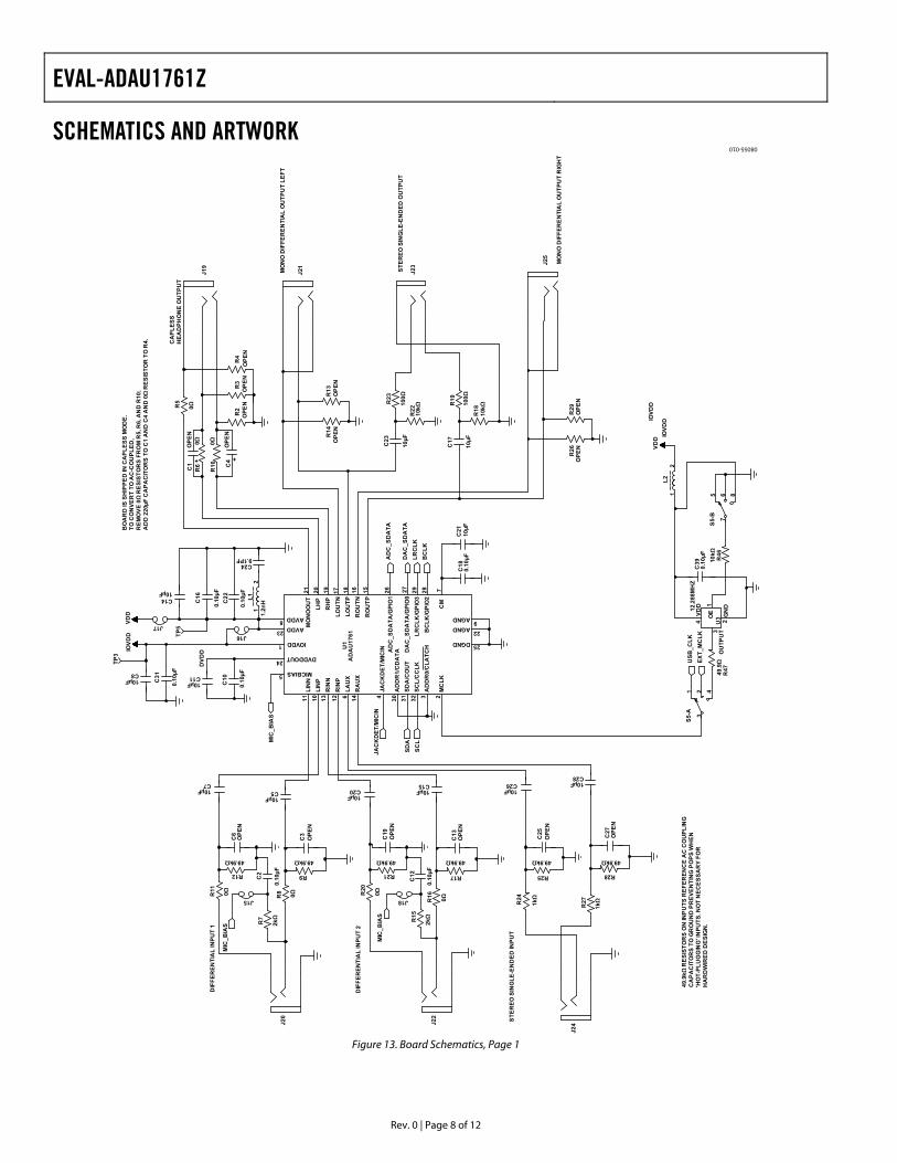
SCHEMATICS AND ARTWORK
08055-010
J25
J23
J19
J21
R4
OPE
N
C16
0.10
µFC
10
0.10
µF
C22
0.10
µF
C31
0.10
µF
R46
10kΩ
C39
0.10
µF1
OE
2G
ND
3O
UTP
UT
4VD
D
U3
12.2
88M
HZ
C21
10µF
C18
0.10
µF
R12
49.9kΩ 49.9kΩ 49.9kΩ 49.9kΩ 49.9kΩ 49.9kΩ
C6
OPE
N
R9
C3
OPE
N
C510µF
C710µF C20
10µF
C1510µF
C2610µF
C2810µF
J20
R21 R17 R25 R28
C19
OPE
N
C13
OPE
N
J22
R23
100Ω
100Ω
C23
10µF
C25
OPE
N
C27
OPE
N
J24
R22
10kΩ
C1410µF
R19
C17
10µF
R18
10kΩ
R2
OPE
NR
3O
PEN
R13
OPE
N
J16J17
12
L2
R4749.9Ω
12
L1
1.2n
H
C249.1PF
31 2 4
S5-A
75 6 8
S5-B
R24
1kΩ
1kΩ
R27
R11
R8 0Ω0Ω R20
0Ω
0ΩR16
R7
2kΩ R15
2kΩ
J18J15
R26
OPE
NR
29O
PEN
R5
0Ω
R14
OPE
N
C810µF C11
10µF
C2
0.10
µF
C12
0.10
µF
1 IOVDD
2M
CLK
3A
DD
R0/
CLA
TCH
4JA
CK
DE
T/M
ICIN
5 MICBIAS
6LA
UX
7C
M
8 AVDD 9AGND
10LI
NP
11LI
NN
12R
INP
13R
INN
14R
AU
X15
RO
UTP
16R
OU
TN
17LO
UTN
18LO
UTP
19R
HP
20LH
P
21M
ON
OO
UT
22AGND23 AVDD
24 DVDDOUT
25DGND
26A
DC
_SD
ATA
/GPI
O1
27D
AC
_SD
ATA
/GPI
O0
28B
CLK
/GPI
O2
29LR
CLK
/GPI
O3
30A
DD
R1/
CD
ATA
31SD
A/C
OU
T32
SCL/
CC
LK
U1
AD
AU
1761
TP3
TP5
+C
4O
PEN
+C
1O
PEN
R6
0Ω
R10
0Ω
AD
C_S
DA
TA
DA
C_S
DA
TALR
CLK
BC
LK
JAC
KD
ET/
MIC
IN
SDA
SCL
EXT_
MC
LK
IOVD
D
IOVD
D
IOVD
DVD
D
USB
_CLK
MIC
_BIA
S
MIC
_BIA
S
MIC
_BIA
S
DV
DD
VDD
Figure 13. Board Schematics, Page 1

EVAL-ADAU1761Z
Rev. 0 | Page 9 of 12
CO
NTR
OL
PO
RT
INTE
RFA
CE
SER
IAL
DA
TA IN
TER
FAC
E
DV
DD
= +
1.8V
(SH
OW
N) O
R +
3.3
V S
UPP
LY
+5V
SUPP
LY F
RO
M U
SBi
DIG
ITA
L M
ICR
OPH
ON
E IN
PUT
JAC
K D
ETEC
T S
IGN
AL
BA
TTER
Y IN
PU
T
1V8
3V3
PLA
NE
DE
CO
UP
LIN
G
RIGHT DMICLEFT DMIC
1 3 5 7 9
2 4 6 8 10
J1
HEA
DER
_10W
AY_
POL
13579
246810
J62x5
R31
10kΩ
R30
10kΩ
C38
0.10
µF
R38
49.9Ω
S4
R44
10kΩ S3
R42
10kΩ
R41
100Ω R40
100Ω
J13
J11
J14
J12 J1
0
J9
R45
10kΩ
R43
10kΩ
1 234
S2
SPST
_2SE
C_S
MD
C9 0.10
µF
D2
GR
EEN
DIF
FUSE
D
D3
YELL
OW
DIF
FUSE
D
R35
140kΩ
C36 0.10
µF
C35
10nF
C33
0.10
µF
C32
10µF
2 13J2 R
APC
722X
C37
10µF
J5
ABJ7
JUMPER2SIP3
J3
OPE
N
R1
100Ω
R48
100Ω
R33
147kΩ
J8R
39
10kΩ
7IN
18
IN2
6SD
4GN
D
1O
UT1
2O
UT2
3O
UT3
5FB U
2
AD
P333
6
TP2
TP1
TP4
TP6
R32
10kΩ
C34
0.10
µFD
1
RE
D D
IFFU
SE
D
R34
169kΩ
S1
SPD
T
KA
D4
13579
2468101211
J4
SO
CK
ET_1
2WA
Y_U
NS
HR
OU
D
R36
10kΩ
R37
10kΩ
C29
0.10
µFC
300.
10µF
C40
0.10
µFC
410.
10µF
M1
PO
LAR
IZIN
G P
LUG
M2
PO
LAR
IZIN
G P
LUG
SCL
SDA
+5V
EXT_
MC
LKLR
CLK
BC
LKD
AC
_SD
ATA
AD
C_S
DA
TA
IOVD
D
BR
D_R
ESE
T
USB
_CLK
IOVD
D
BC
LK
+5V
JAC
KD
ET/
MIC
IN
VDD
IOVD
D
VDD
BR
D_R
ESE
T
BC
LK
AD
C_S
DA
TA
DA
C_S
DA
TA
LRC
LK
08055-011
Figure 14. Board Schematics, Page 2

EVAL-ADAU1761Z
Rev. 0 | Page 10 of 12
0805
5-01
2
Figure 15. Board Silkscreen and Parts Placement
EVAL-ADAU1761Z
Rev. 0 | Page 11 of 12
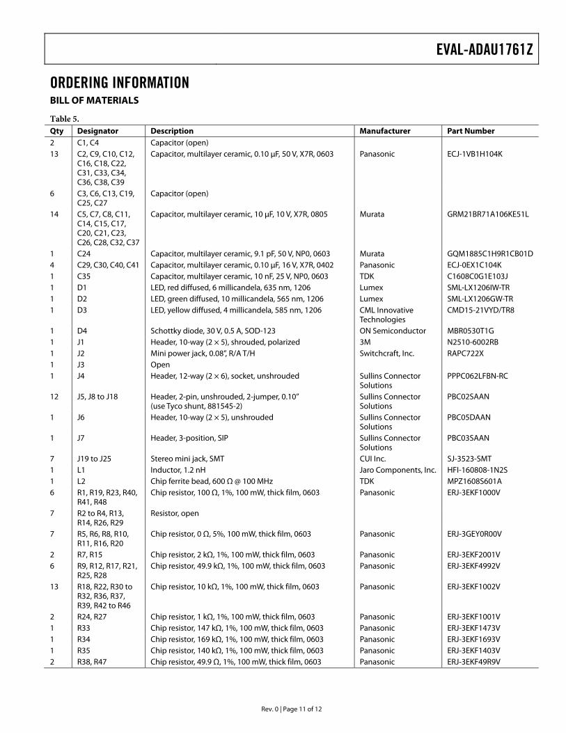
ORDERING INFORMATION BILL OF MATERIALS
Table 5. Qty Designator Description Manufacturer Part Number 2 C1, C4 Capacitor (open) 13 C2, C9, C10, C12,
C16, C18, C22, C31, C33, C34, C36, C38, C39
Capacitor, multilayer ceramic, 0.10 μF, 50 V, X7R, 0603 Panasonic ECJ-1VB1H104K
6 C3, C6, C13, C19, C25, C27
Capacitor (open)
14 C5, C7, C8, C11, C14, C15, C17, C20, C21, C23, C26, C28, C32, C37
Capacitor, multilayer ceramic, 10 μF, 10 V, X7R, 0805 Murata GRM21BR71A106KE51L
1 C24 Capacitor, multilayer ceramic, 9.1 pF, 50 V, NP0, 0603 Murata GQM1885C1H9R1CB01D 4 C29, C30, C40, C41 Capacitor, multilayer ceramic, 0.10 μF, 16 V, X7R, 0402 Panasonic ECJ-0EX1C104K 1 C35 Capacitor, multilayer ceramic, 10 nF, 25 V, NP0, 0603 TDK C1608C0G1E103J 1 D1 LED, red diffused, 6 millicandela, 635 nm, 1206 Lumex SML-LX1206IW-TR 1 D2 LED, green diffused, 10 millicandela, 565 nm, 1206 Lumex SML-LX1206GW-TR 1 D3 LED, yellow diffused, 4 millicandela, 585 nm, 1206 CML Innovative
Technologies CMD15-21VYD/TR8
1 D4 Schottky diode, 30 V, 0.5 A, SOD-123 ON Semiconductor MBR0530T1G 1 J1 Header, 10-way (2 × 5), shrouded, polarized 3M N2510-6002RB 1 J2 Mini power jack, 0.08”, R/A T/H Switchcraft, Inc. RAPC722X 1 J3 Open 1 J4 Header, 12-way (2 × 6), socket, unshrouded Sullins Connector
Solutions PPPC062LFBN-RC
12 J5, J8 to J18 Header, 2-pin, unshrouded, 2-jumper, 0.10” (use Tyco shunt, 881545-2)
Sullins Connector Solutions
PBC02SAAN
1 J6 Header, 10-way (2 × 5), unshrouded Sullins Connector Solutions
PBC05DAAN
1 J7 Header, 3-position, SIP Sullins Connector Solutions
PBC03SAAN
7 J19 to J25 Stereo mini jack, SMT CUI Inc. SJ-3523-SMT 1 L1 Inductor, 1.2 nH Jaro Components, Inc. HFI-160808-1N2S 1 L2 Chip ferrite bead, 600 Ω @ 100 MHz TDK MPZ1608S601A 6 R1, R19, R23, R40,
R41, R48 Chip resistor, 100 Ω, 1%, 100 mW, thick film, 0603 Panasonic ERJ-3EKF1000V
7 R2 to R4, R13, R14, R26, R29
Resistor, open
7 R5, R6, R8, R10, R11, R16, R20
Chip resistor, 0 Ω, 5%, 100 mW, thick film, 0603 Panasonic ERJ-3GEY0R00V
2 R7, R15 Chip resistor, 2 kΩ, 1%, 100 mW, thick film, 0603 Panasonic ERJ-3EKF2001V 6 R9, R12, R17, R21,
R25, R28 Chip resistor, 49.9 kΩ, 1%, 100 mW, thick film, 0603 Panasonic ERJ-3EKF4992V
13 R18, R22, R30 to R32, R36, R37, R39, R42 to R46
Chip resistor, 10 kΩ, 1%, 100 mW, thick film, 0603 Panasonic ERJ-3EKF1002V
2 R24, R27 Chip resistor, 1 kΩ, 1%, 100 mW, thick film, 0603 Panasonic ERJ-3EKF1001V 1 R33 Chip resistor, 147 kΩ, 1%, 100 mW, thick film, 0603 Panasonic ERJ-3EKF1473V 1 R34 Chip resistor, 169 kΩ, 1%, 100 mW, thick film, 0603 Panasonic ERJ-3EKF1693V 1 R35 Chip resistor, 140 kΩ, 1%, 100 mW, thick film, 0603 Panasonic ERJ-3EKF1403V 2 R38, R47 Chip resistor, 49.9 Ω, 1%, 100 mW, thick film, 0603 Panasonic ERJ-3EKF49R9V

EVAL-ADAU1761Z
Rev. 0 | Page 12 of 12
Qty Designator Description Manufacturer Part Number 1 S1 Slide switch, SPDT, PC mount, L = 2 mm E-Switch EG1271 1 S2 SMD dip switch, 2-section SPST, raised actuator CTS Corporation 219-2LPST 2 S3, S4 Tact switch, long stroke (normally open) Omron Electronics B3M-6009 1 S5 Slide switch, DP3T, PC mount, L = 4 mm E-Switch EG2305 6 TP1 to TP6 Mini test point, white, 0.1” OD Keystone Electronics 5002 1 U1 SigmaDSP codec Analog Devices ADAU1761BCPZ 1 U2 Adjustable low dropout voltage regulator Analog Devices ADP3336ARMZ 1 U3 SMD oscillator, 12.288 MHz, fixed, 1.8 VDC to 3.3 VDC Abracon Corporation AP3S-12.288MHz-F-J-B
ESD CAUTION ORDERING GUIDE Model Description EVAL-ADAU1761Z1 Evaluation Board
1 Z = RoHS Compliant Part.
Purchase of licensed I2C components of Analog Devices or one of its sublicensed Associated Companies conveys a license for the purchaser under the Philips I2C Patent Rights to use these components in an I2C system, provided that the system conforms to the I2C Standard Specification as defined by Philips.
©2009 Analog Devices, Inc. All rights reserved. Trademarks and registered trademarks are the property of their respective owners. EB08055-0-5/09(0)