Embed Size (px)
Citation preview
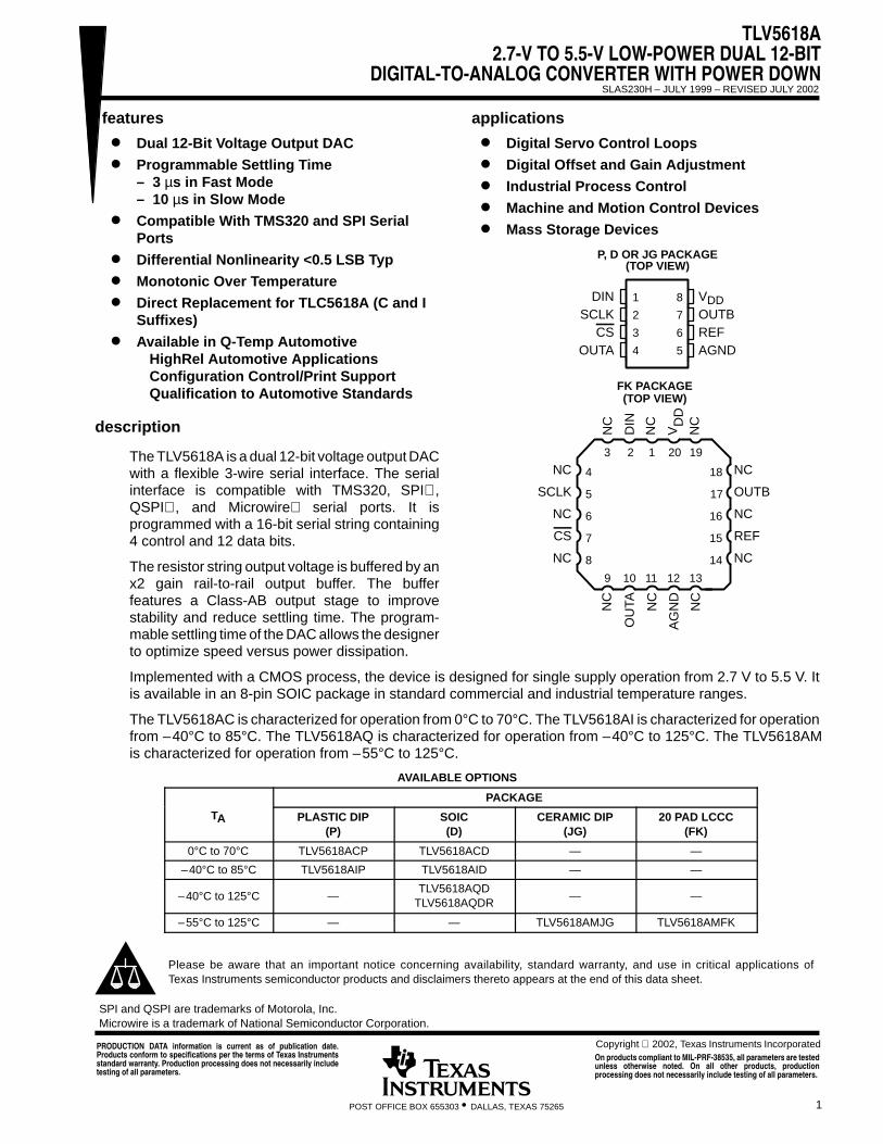
TLV5618A2.7-V TO 5.5-V LOW-POWER DUAL 12-BIT
DIGITAL-TO-ANALOG CONVERTER WITH POWER DOWNSLAS230H – JULY 1999 – REVISED JULY 2002
1POST OFFICE BOX 655303 • DALLAS, TEXAS 75265
features
Dual 12-Bit Voltage Output DAC
Programmable Settling Time– 3 µs in Fast Mode– 10 µs in Slow Mode
Compatible With TMS320 and SPI SerialPorts
Differential Nonlinearity <0.5 LSB Typ
Monotonic Over Temperature
Direct Replacement for TLC5618A (C and ISuffixes)
Available in Q-Temp Automotive HighRel Automotive ApplicationsConfiguration Control/Print SupportQualification to Automotive Standards
applications
Digital Servo Control Loops
Digital Offset and Gain Adjustment
Industrial Process Control
Machine and Motion Control Devices
Mass Storage Devices
description
The TLV5618A is a dual 12-bit voltage output DACwith a flexible 3-wire serial interface. The serialinterface is compatible with TMS320, SPI ,QSPI , and Microwire serial ports. It isprogrammed with a 16-bit serial string containing4 control and 12 data bits.
The resistor string output voltage is buffered by anx2 gain rail-to-rail output buffer. The bufferfeatures a Class-AB output stage to improvestability and reduce settling time. The program-mable settling time of the DAC allows the designerto optimize speed versus power dissipation.
Implemented with a CMOS process, the device is designed for single supply operation from 2.7 V to 5.5 V. Itis available in an 8-pin SOIC package in standard commercial and industrial temperature ranges.
The TLV5618AC is characterized for operation from 0°C to 70°C. The TLV5618AI is characterized for operationfrom –40°C to 85°C. The TLV5618AQ is characterized for operation from –40°C to 125°C. The TLV5618AMis characterized for operation from –55°C to 125°C.
AVAILABLE OPTIONS
PACKAGE
TA PLASTIC DIP(P)
SOIC(D)
CERAMIC DIP(JG)
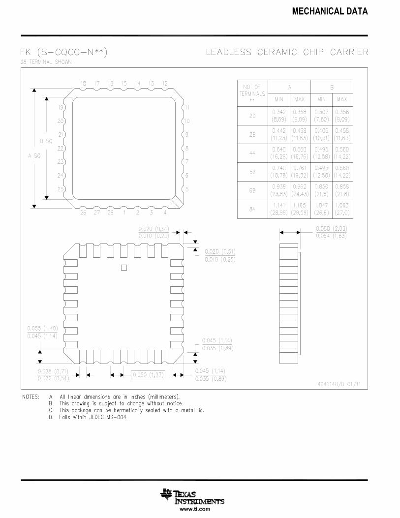
20 PAD LCCC(FK)
0°C to 70°C TLV5618ACP TLV5618ACD — —
–40°C to 85°C TLV5618AIP TLV5618AID — —
–40°C to 125°C —TLV5618AQD
TLV5618AQDR— —
–55°C to 125°C — — TLV5618AMJG TLV5618AMFK
Please be aware that an important notice concerning availability, standard warranty, and use in critical applications ofTexas Instruments semiconductor products and disclaimers thereto appears at the end of this data sheet.
Copyright 2002, Texas Instruments IncorporatedPRODUCTION DATA information is current as of publication date.Products conform to specifications per the terms of Texas Instrumentsstandard warranty. Production processing does not necessarily includetesting of all parameters.
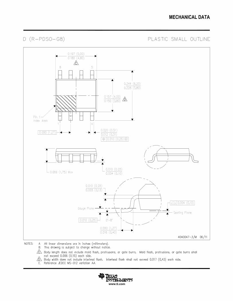
1
2
3
4
8
7
6
5
DINSCLK
CSOUTA
VDDOUTBREFAGND
P, D OR JG PACKAGE(TOP VIEW)
192013 2
17
18
16
15
14
1312119 10
5
4
6
7
8
NC
OUTB
NC
REF
NC
NC
SCLK
NC
CS
NC
NC
DIN
NC
V NC
OU
TA NC
AG
ND
NC
NC
FK PACKAGE(TOP VIEW)
DD
On products compliant to MIL-PRF-38535, all parameters are testedunless otherwise noted. On all other products, productionprocessing does not necessarily include testing of all parameters.
SPI and QSPI are trademarks of Motorola, Inc.Microwire is a trademark of National Semiconductor Corporation.
TLV5618A2.7-V TO 5.5-V LOW-POWER DUAL 12-BITDIGITAL-TO-ANALOG CONVERTER WITH POWER DOWNSLAS230H – JULY 1999 – REVISED JULY 2002
2 POST OFFICE BOX 655303 • DALLAS, TEXAS 75265
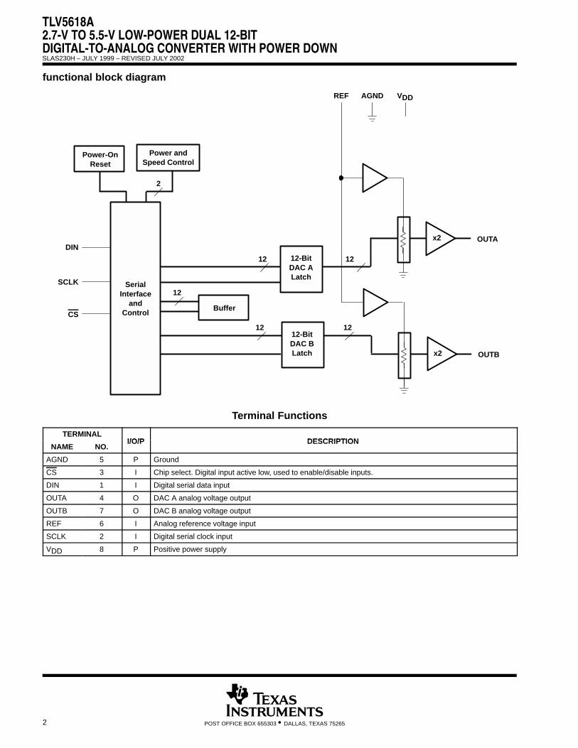
functional block diagram
SerialInterface
andControl
12-BitDAC BLatch
SCLK
DIN
CS
OUTA
Power-OnReset
x2
12
Power andSpeed Control
2
12-BitDAC ALatch
12
REF AGND VDD
12 12
OUTBx2
Buffer
12
Terminal Functions
TERMINALI/O/P DESCRIPTION
NAME NO.I/O/P DESCRIPTION
AGND 5 P Ground
CS 3 I Chip select. Digital input active low, used to enable/disable inputs.
DIN 1 I Digital serial data input
OUTA 4 O DAC A analog voltage output
OUTB 7 O DAC B analog voltage output
REF 6 I Analog reference voltage input
SCLK 2 I Digital serial clock input
VDD 8 P Positive power supply
TLV5618A2.7-V TO 5.5-V LOW-POWER DUAL 12-BIT
DIGITAL-TO-ANALOG CONVERTER WITH POWER DOWNSLAS230H – JULY 1999 – REVISED JULY 2002
3POST OFFICE BOX 655303 • DALLAS, TEXAS 75265
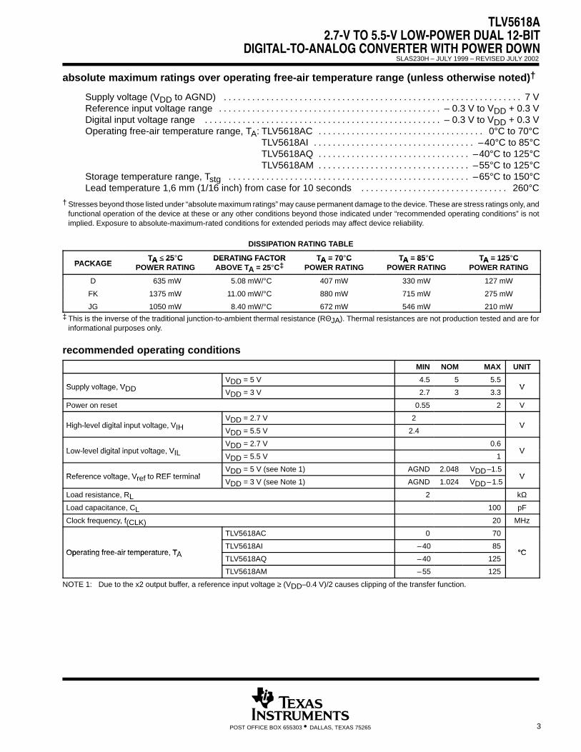
absolute maximum ratings over operating free-air temperature range (unless otherwise noted)†
Supply voltage (VDD to AGND) 7 V. . . . . . . . . . . . . . . . . . . . . . . . . . . . . . . . . . . . . . . . . . . . . . . . . . . . . . . . . . . . . . . Reference input voltage range – 0.3 V to VDD + 0.3 V. . . . . . . . . . . . . . . . . . . . . . . . . . . . . . . . . . . . . . . . . . . . . . . Digital input voltage range – 0.3 V to VDD + 0.3 V. . . . . . . . . . . . . . . . . . . . . . . . . . . . . . . . . . . . . . . . . . . . . . . . . . Operating free-air temperature range, TA: TLV5618AC 0°C to 70°C. . . . . . . . . . . . . . . . . . . . . . . . . . . . . . . . . . .
TLV5618AI –40°C to 85°C. . . . . . . . . . . . . . . . . . . . . . . . . . . . . . . . . . TLV5618AQ –40°C to 125°C. . . . . . . . . . . . . . . . . . . . . . . . . . . . . . . . TLV5618AM –55°C to 125°C. . . . . . . . . . . . . . . . . . . . . . . . . . . . . . . .
Storage temperature range, Tstg –65°C to 150°C. . . . . . . . . . . . . . . . . . . . . . . . . . . . . . . . . . . . . . . . . . . . . . . . . . . Lead temperature 1,6 mm (1/16 inch) from case for 10 seconds 260°C. . . . . . . . . . . . . . . . . . . . . . . . . . . . . . .
† Stresses beyond those listed under “absolute maximum ratings” may cause permanent damage to the device. These are stress ratings only, andfunctional operation of the device at these or any other conditions beyond those indicated under “recommended operating conditions” is notimplied. Exposure to absolute-maximum-rated conditions for extended periods may affect device reliability.
DISSIPATION RATING TABLE
PACKAGETA ≤ 25°C DERATING FACTOR TA = 70°C TA = 85°C TA = 125°C
PACKAGETA ≤ 25 C
POWER RATINGDERATING FACTORABOVE TA = 25°C‡
TA = 70 CPOWER RATING
TA = 85 CPOWER RATING
TA = 125 CPOWER RATING
D 635 mW 5.08 mW/°C 407 mW 330 mW 127 mW
FK 1375 mW 11.00 mW/°C 880 mW 715 mW 275 mW
JG 1050 mW 8.40 mW/°C 672 mW 546 mW 210 mW‡ This is the inverse of the traditional junction-to-ambient thermal resistance (RΘJA). Thermal resistances are not production tested and are for
informational purposes only.
recommended operating conditions
MIN NOM MAX UNIT
Supply voltage VVDD = 5 V 4.5 5 5.5
VSupply voltage, VDD VDD = 3 V 2.7 3 3.3V
Power on reset 0.55 2 V
High level digital input voltage VVDD = 2.7 V 2
VHigh-level digital input voltage, VIH VDD = 5.5 V 2.4V
Low level digital input voltage VVDD = 2.7 V 0.6
VLow-level digital input voltage, VIL VDD = 5.5 V 1V
Reference voltage V to REF terminalVDD = 5 V (see Note 1) AGND 2.048 VDD–1.5
VReference voltage, Vref to REF terminalVDD = 3 V (see Note 1) AGND 1.024 VDD–1.5
V
Load resistance, RL 2 kΩ
Load capacitance, CL 100 pF
Clock frequency, f(CLK) 20 MHz
TLV5618AC 0 70
Operating free air temperature TATLV5618AI –40 85
°COperating free-air temperature, TATLV5618AQ –40 125
°C
TLV5618AM –55 125
NOTE 1: Due to the x2 output buffer, a reference input voltage ≥ (VDD–0.4 V)/2 causes clipping of the transfer function.
TLV5618A2.7-V TO 5.5-V LOW-POWER DUAL 12-BITDIGITAL-TO-ANALOG CONVERTER WITH POWER DOWNSLAS230H – JULY 1999 – REVISED JULY 2002
4 POST OFFICE BOX 655303 • DALLAS, TEXAS 75265
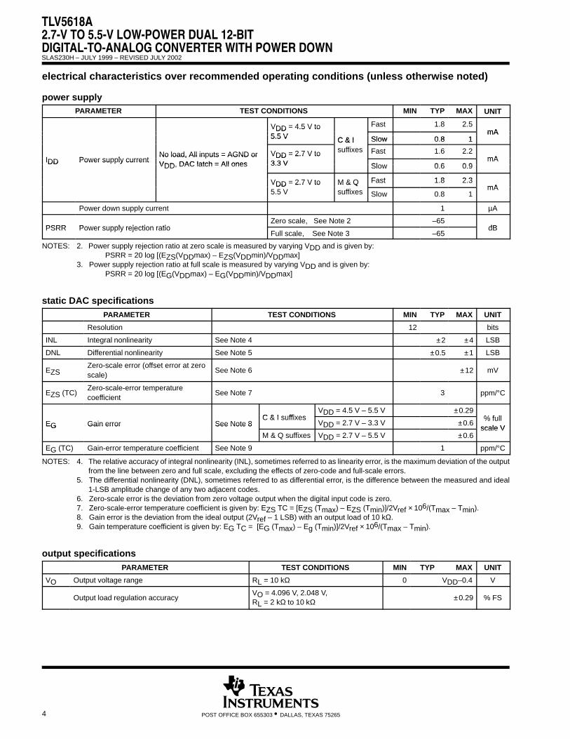
electrical characteristics over recommended operating conditions (unless otherwise noted)
power supplyPARAMETER TEST CONDITIONS MIN TYP MAX UNIT
VDD = 4.5 V to Fast 1.8 2.5mA
VDD 4.5 V to5 5 V
mA5.5 V C & I Slow 0 8 1mA5.5 V C & I Slow 0.8 1
I Power supply currentNo load, All inputs = AGND or VDD = 2.7 V to
C & Isuffixes Fast 1.6 2.2
mAIDD Power supply currentNo load, All in uts = AGND orVDD DAC latch = All ones
VDD 2.7 V to3 3 V Slow 0 6 0 9
mAIDD Power su ly current VDD, DAC latch = All ones 3.3 V Slow 0.6 0.9
Fast 1 8 2 3VDD = 2.7 V to M & Q Fast 1.8 2.3mA
VDD 2.7 V to5.5 V
M & Qsuffixes Slow 0.8 1
mA
Power down supply current 1 µA
PSRR Power supply rejection ratioZero scale, See Note 2 –65
dBPSRR Power supply rejection ratioFull scale, See Note 3 –65
dB
NOTES: 2. Power supply rejection ratio at zero scale is measured by varying VDD and is given by:PSRR = 20 log [(EZS(VDDmax) – EZS(VDDmin)/VDDmax]
3. Power supply rejection ratio at full scale is measured by varying VDD and is given by:PSRR = 20 log [(EG(VDDmax) – EG(VDDmin)/VDDmax]
static DAC specificationsPARAMETER TEST CONDITIONS MIN TYP MAX UNIT
Resolution 12 bits
INL Integral nonlinearity See Note 4 ±2 ±4 LSB
DNL Differential nonlinearity See Note 5 ±0.5 ±1 LSB
EZSZero-scale error (offset error at zeroscale)
See Note 6 ±12 mV
EZS (TC)Zero-scale-error temperature coefficient
See Note 7 3 ppm/°C
C & I suffixesVDD = 4.5 V – 5.5 V ±0.29
% f llEG Gain error See Note 8
C & I suffixesVDD = 2.7 V – 3.3 V ±0.6
% fullscale V
EG Gain error See Note 8
M & Q suffixes VDD = 2.7 V – 5.5 V ±0.6scale V
EG (TC) Gain-error temperature coefficient See Note 9 1 ppm/°C
NOTES: 4. The relative accuracy of integral nonlinearity (INL), sometimes referred to as linearity error, is the maximum deviation of the outputfrom the line between zero and full scale, excluding the effects of zero-code and full-scale errors.
5. The differential nonlinearity (DNL), sometimes referred to as differential error, is the difference between the measured and ideal1-LSB amplitude change of any two adjacent codes.
6. Zero-scale error is the deviation from zero voltage output when the digital input code is zero.7. Zero-scale-error temperature coefficient is given by: EZS TC = [EZS (Tmax) – EZS (Tmin)]/2Vref × 106/(Tmax – Tmin).8. Gain error is the deviation from the ideal output (2Vref – 1 LSB) with an output load of 10 kΩ.9. Gain temperature coefficient is given by: EG TC = [EG (Tmax) – Eg (Tmin)]/2Vref × 106/(Tmax – Tmin).
output specificationsPARAMETER TEST CONDITIONS MIN TYP MAX UNIT
VO Output voltage range RL = 10 kΩ 0 VDD–0.4 V
Output load regulation accuracyVO = 4.096 V, 2.048 V, RL = 2 kΩ to 10 kΩ ±0.29 % FS
TLV5618A2.7-V TO 5.5-V LOW-POWER DUAL 12-BIT
DIGITAL-TO-ANALOG CONVERTER WITH POWER DOWNSLAS230H – JULY 1999 – REVISED JULY 2002
5POST OFFICE BOX 655303 • DALLAS, TEXAS 75265
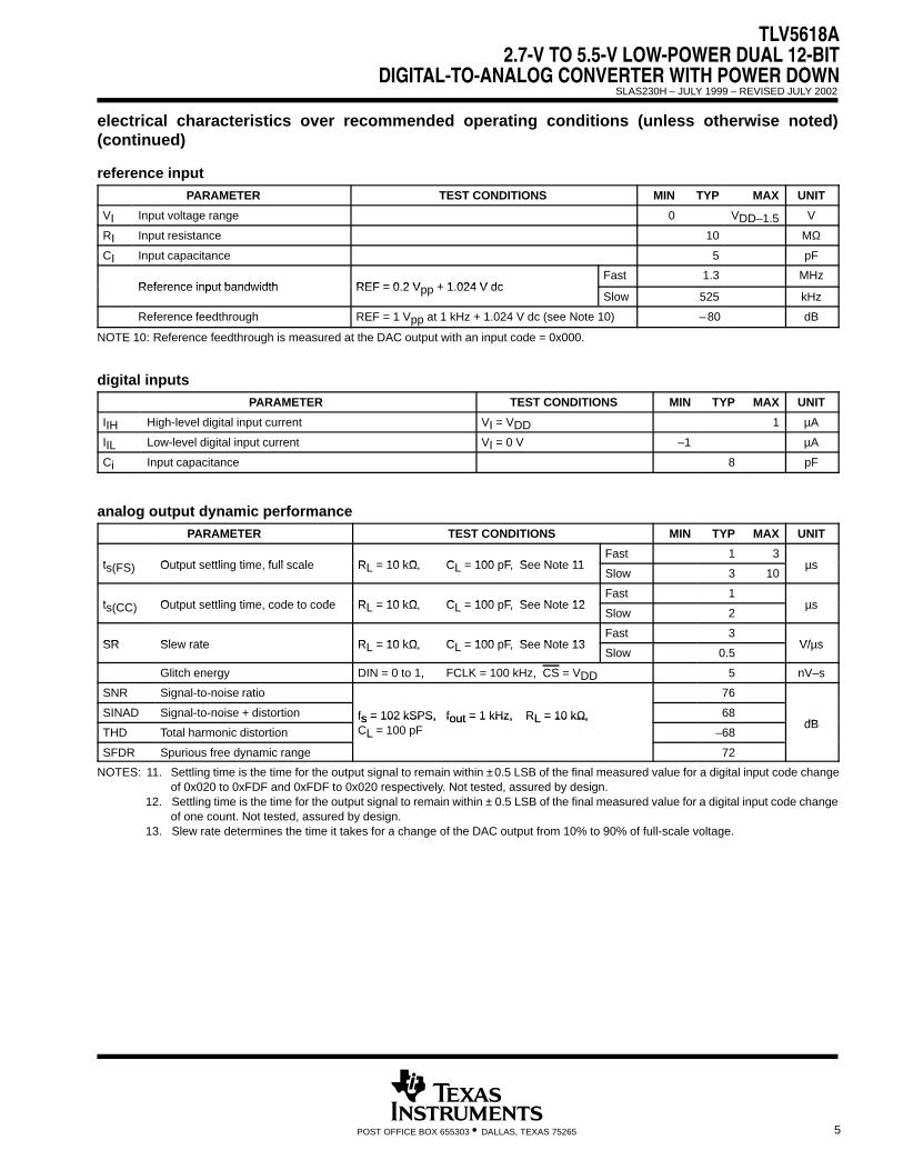
electrical characteristics over recommended operating conditions (unless otherwise noted)(continued)
reference inputPARAMETER TEST CONDITIONS MIN TYP MAX UNIT
VI Input voltage range 0 VDD–1.5 V
RI Input resistance 10 MΩ
CI Input capacitance 5 pF
Reference input bandwidth REF = 0 2 V + 1 024 V dcFast 1.3 MHz
Reference input bandwidth REF = 0.2 Vpp + 1.024 V dcSlow 525 kHz
Reference feedthrough REF = 1 Vpp at 1 kHz + 1.024 V dc (see Note 10) –80 dB
NOTE 10: Reference feedthrough is measured at the DAC output with an input code = 0x000.
digital inputsPARAMETER TEST CONDITIONS MIN TYP MAX UNIT
IIH High-level digital input current VI = VDD 1 µA
IIL Low-level digital input current VI = 0 V –1 µA
Ci Input capacitance 8 pF
analog output dynamic performancePARAMETER TEST CONDITIONS MIN TYP MAX UNIT
t Output settling time full scale R 10 kΩ C 100 pF See Note 11Fast 1 3
sts(FS) Output settling time, full scale RL = 10 kΩ, CL = 100 pF, See Note 11Slow 3 10
µs
t Output settling time code to code R 10 kΩ C 100 pF See Note 12Fast 1
sts(CC) Output settling time, code to code RL = 10 kΩ, CL = 100 pF, See Note 12Slow 2
µs
SR Slew rate R 10 kΩ C 100 pF See Note 13Fast 3
V/ sSR Slew rate RL = 10 kΩ, CL = 100 pF, See Note 13Slow 0.5
V/µs
Glitch energy DIN = 0 to 1, FCLK = 100 kHz, CS = VDD 5 nV–s
SNR Signal-to-noise ratio 76
SINAD Signal-to-noise + distortion fs = 102 kSPS, fout = 1 kHz, RL = 10 kΩ, 68dB
THD Total harmonic distortion
fs = 102 kSPS, fout = 1 kHz, RL = 10 kΩ,CL = 100 pF –68
dB
SFDR Spurious free dynamic range
L
72
NOTES: 11. Settling time is the time for the output signal to remain within ±0.5 LSB of the final measured value for a digital input code changeof 0x020 to 0xFDF and 0xFDF to 0x020 respectively. Not tested, assured by design.
12. Settling time is the time for the output signal to remain within ± 0.5 LSB of the final measured value for a digital input code changeof one count. Not tested, assured by design.
13. Slew rate determines the time it takes for a change of the DAC output from 10% to 90% of full-scale voltage.
TLV5618A2.7-V TO 5.5-V LOW-POWER DUAL 12-BITDIGITAL-TO-ANALOG CONVERTER WITH POWER DOWNSLAS230H – JULY 1999 – REVISED JULY 2002
6 POST OFFICE BOX 655303 • DALLAS, TEXAS 75265
digital input timing requirements
MIN NOM MAX UNIT
C and I suffixesVDD = 5 V 5
nstsu(CS-CK) Setup time, CS low before first negative SCLK edge
C and I suffixesVDD = 3 V 10
nstsu(CS-CK) Setu time, CS low before first negative SCLK edge
Q and M suffixes 10 ns
tsu(C16-CS) Setup time, 16th negative SCLK edge before CS rising edge 10 ns
tw(H) SCLK pulse width high 25 ns
tw(L) SCLK pulse width low 25 ns
C and I suffixesVDD = 5 V 5
tsu(D) Setup time, data ready before SCLK falling edgeC and I suffixes
VDD = 3 V 10 nstsu(D) Setu time, data ready before SCLK falling edge
Q and M suffixes 8
ns
C and I suffixesVDD = 5 V 5
th(D) Hold time, data held valid after SCLK falling edgeC and I suffixes
VDD = 3 V 10 nsh(D) g g
Q and M suffixes 10
th(CSH) Hold time CS high between cyclesVDD = 5 V 25
nsth(CSH) Hold time, CS high between cyclesVDD = 3 V 50
ns
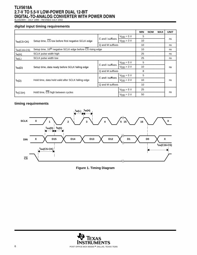
timing requirements
tw(L)
SCLK
CS
DIN D15 D14 D13 D12 D1 D0 XX
1X 2 3 4 5 15 16 X
tw(H)
tsu(D) th(D)
tsu(CS-CK)
tsu(C16-CS)
Figure 1. Timing Diagram

TLV5618A2.7-V TO 5.5-V LOW-POWER DUAL 12-BIT
DIGITAL-TO-ANALOG CONVERTER WITH POWER DOWNSLAS230H – JULY 1999 – REVISED JULY 2002
7POST OFFICE BOX 655303 • DALLAS, TEXAS 75265
TYPICAL CHARACTERISTICS
Figure 2
2.046
2.044
2.040
2.038
2.036
2.050
2.042
2.048
Load Current – mA
OUTPUT VOLTAGEvs
LOAD CURRENT
– O
utp
ut
Vo
ltag
e –
VV
O
VDD = 3 VVREF = 1 VFull Scale
3 V Slow Mode, SOURCE
3 V Fast Mode, SOURCE
0 –0.01 –0.02 –0.5 –0.1 –0.2 –0.5 –1 –2–0.8
Figure 3
4.095
4.090
4.080
4.075
4.070
4.105
4.085
4.100
OUTPUT VOLTAGEvs
LOAD CURRENT
– O
utp
ut
Vo
ltag
e –
VV
O
VDD = 5 VVREF = 2 VFull Scale
5 V Slow Mode, SOURCE
5 V Fast Mode, SOURCE
Load Current – mA0 –0.02 –0.04 –0.1 –0.2 –0.4 –1 –2 –4–0.8
Figure 4
0.16
0.14
0.10
0.08
0.06
0.20
0.12
0.18
Load Current – mA
OUTPUT VOLTAGEvs
LOAD CURRENT
– O
utp
ut
Vo
ltag
e –
VV
O
3 V Slow Mode, SINK
3 V Fast Mode, SINK0.04
0.02
0.00
VDD = 3 VVREF = 1 VZero Scale
0 0.01 0.02 0.05 0.1 0.2 0.5 1 20.8
Figure 5
0.25
0.20
0.10
0.05
0.00
0.35
0.15
0.30
Load Current – mA
OUTPUT VOLTAGEvs
LOAD CURRENT
– O
utp
ut
Vo
ltag
e –
VV
O
5 V Slow Mode, SINK
5 V Fast Mode, SINK
VDD = 5 VVREF = 2 VZero Scale
0 0.02 0.04 0.1 0.2 0.4 1 2 40.8
TLV5618A2.7-V TO 5.5-V LOW-POWER DUAL 12-BITDIGITAL-TO-ANALOG CONVERTER WITH POWER DOWNSLAS230H – JULY 1999 – REVISED JULY 2002
8 POST OFFICE BOX 655303 • DALLAS, TEXAS 75265
TYPICAL CHARACTERISTICS
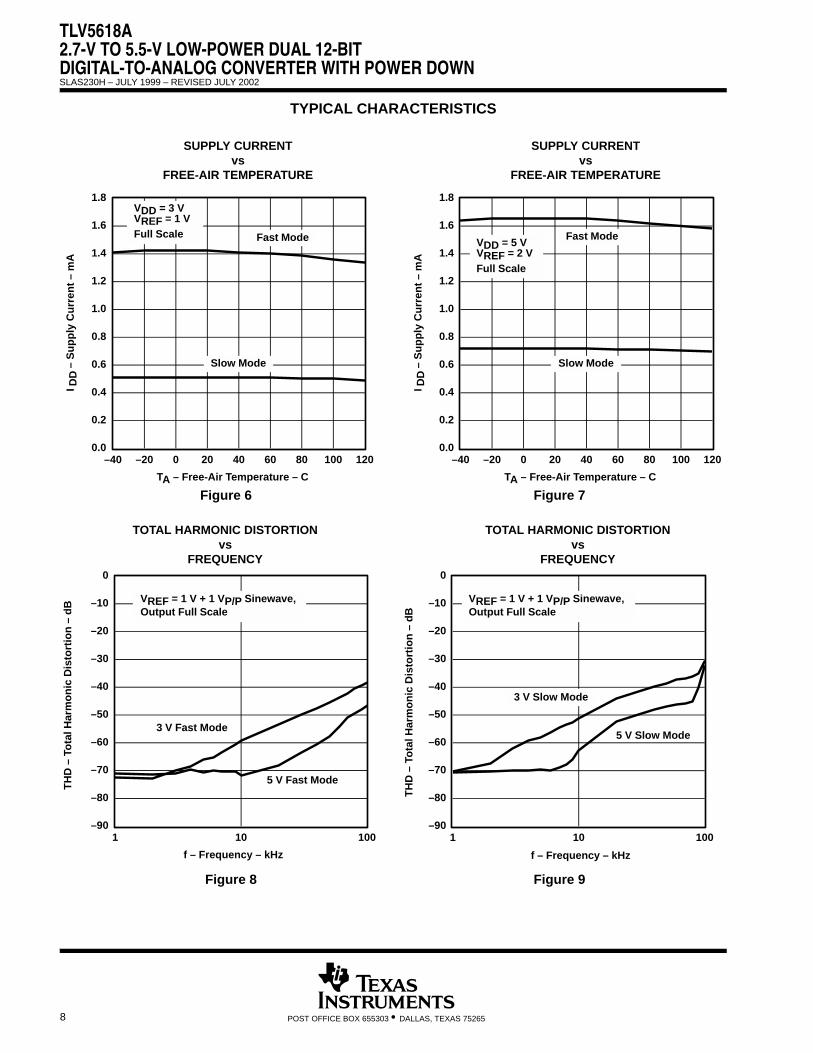
Figure 6
0.0
0.2
0.4
0.6
0.8
1.0
1.2
1.4
1.6
1.8
–40 –20 0 20 40 60 80 100 120
SUPPLY CURRENTvs
FREE-AIR TEMPERATURE
TA – Free-Air Temperature – C
VDD = 3 VVREF = 1 VFull Scale Fast Mode
Slow Mode
I DD
– S
up
ply
Cu
rren
t –
mA
Figure 7
0.0
0.2
0.4
0.6
0.8
1.0
1.2
1.4
1.6
1.8
–40 –20 0 20 40 60 80 100 120
SUPPLY CURRENTvs
FREE-AIR TEMPERATURE
TA – Free-Air Temperature – C
VDD = 5 VVREF = 2 VFull Scale
Fast Mode
Slow Mode
I DD
– S
up
ply
Cu
rren
t –
mA
–90
–80
–70
–60
–50
–40
–30
–20
–10
0
1 10 100
TOTAL HARMONIC DISTORTIONvs
FREQUENCY
VREF = 1 V + 1 VP/P Sinewave,Output Full Scale
3 V Fast Mode
5 V Fast ModeTH
D –
To
tal H
arm
on
ic D
isto
rtio
n –
dB
Figure 8
f – Frequency – kHz
–90
–80
–70
–60
–50
–40
–30
–20
–10
0
1 10 100
TOTAL HARMONIC DISTORTIONvs
FREQUENCY
VREF = 1 V + 1 VP/P Sinewave,Output Full Scale
5 V Slow Mode
TH
D –
To
tal H
arm
on
ic D
isto
rtio
n –
dB
3 V Slow Mode
f – Frequency – kHz
Figure 9
TLV5618A2.7-V TO 5.5-V LOW-POWER DUAL 12-BIT
DIGITAL-TO-ANALOG CONVERTER WITH POWER DOWNSLAS230H – JULY 1999 – REVISED JULY 2002
9POST OFFICE BOX 655303 • DALLAS, TEXAS 75265
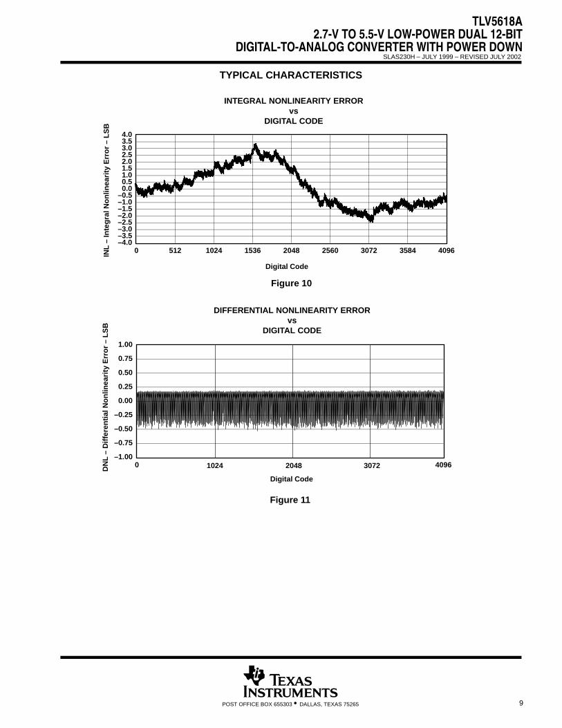
TYPICAL CHARACTERISTICS
–4.0–3.5–3.0–2.5–2.0–1.5–1.0–0.50.00.51.01.52.02.53.03.54.0
0 512 1024 1536 2048 2560 3072 3584 4096INL
– In
teg
ral N
on
linea
rity
Err
or
– L
SB
INTEGRAL NONLINEARITY ERRORvs
DIGITAL CODE
Digital Code
Figure 10
Figure 11
–1.00
–0.75
–0.50
–0.25
0.00
0.25
0.50
0.75
1.00
0 4096
Digital Code
DIFFERENTIAL NONLINEARITY ERRORvs
DIGITAL CODE
20481024 3072DN
L –
Dif
fere
nti
al N
on
linea
rity
Err
or
– L
SB
TLV5618A2.7-V TO 5.5-V LOW-POWER DUAL 12-BITDIGITAL-TO-ANALOG CONVERTER WITH POWER DOWNSLAS230H – JULY 1999 – REVISED JULY 2002
10 POST OFFICE BOX 655303 • DALLAS, TEXAS 75265
APPLICATION INFORMATION
general function
The TLV5618A is a dual 12-bit, single-supply DAC, based on a resistor-string architecture. It consists of a serialinterface, a speed and power down control logic, a resistor string, and a rail-to-rail output buffer.
The output voltage (full scale determined by the reference) is given by:
2 REF CODE2n [V]
Where REF is the reference voltage and CODE is the digital input value within the range of 010 to 2n–1, wheren=12 (bits). The 16-bit data word, consisting of control bits and the new DAC value, is illustrated in the dataformat section. A power-on reset initially resets the internal latches to a defined state (all bits zero).
serial interface
A falling edge of CS starts shifting the data bit-per-bit (starting with the MSB) to the internal register on the fallingedges of SCLK. After 16 bits have been transferred or CS rises, the content of the shift register is moved to thetarget latches (DAC A, DAC B, BUFFER, CONTROL), depending on the control bits within the data word.
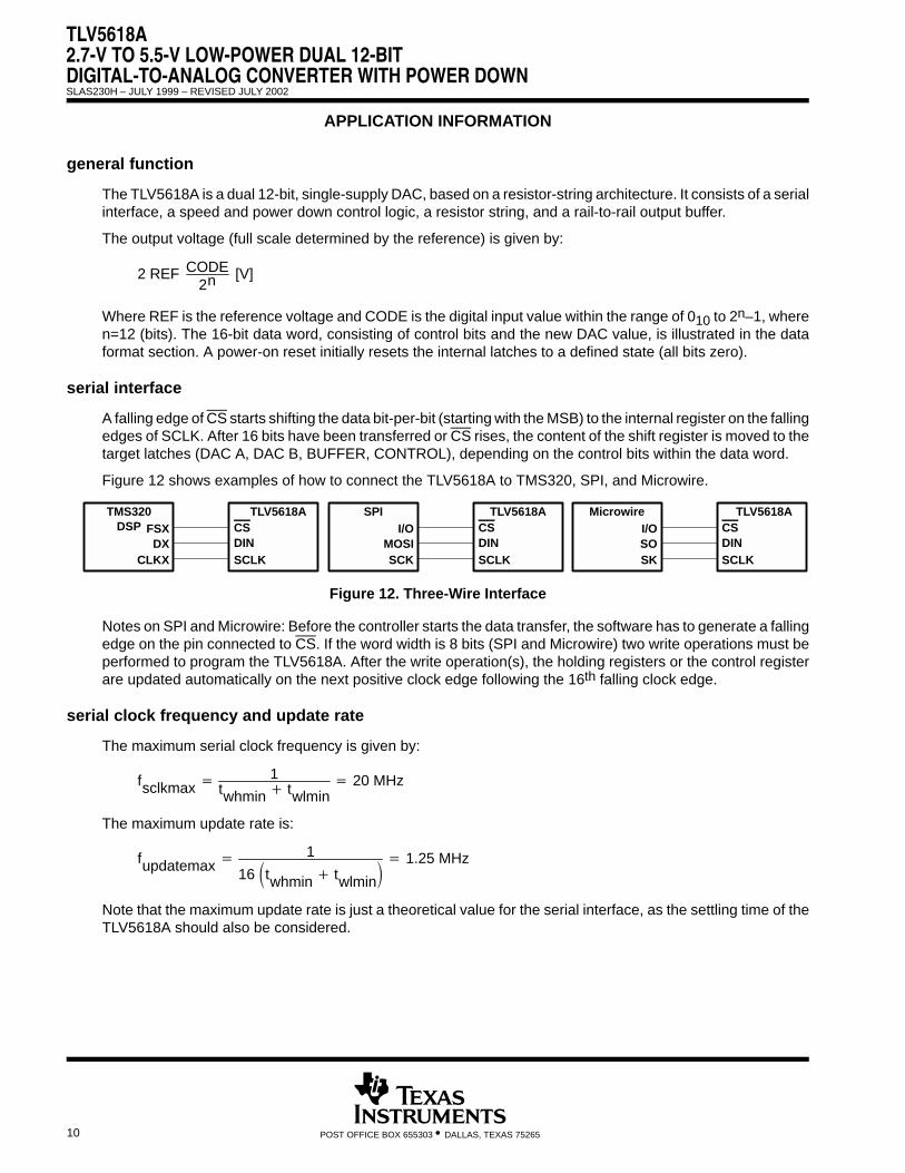
Figure 12 shows examples of how to connect the TLV5618A to TMS320, SPI, and Microwire.
TMS320DSP FSX
CLKXDX
TLV5618A
SCLKDINCS
SPII/O
SCKMOSI
TLV5618A
SCLKDINCS
MicrowireI/O
SKSO
TLV5618A
SCLKDINCS
Figure 12. Three-Wire Interface
Notes on SPI and Microwire: Before the controller starts the data transfer, the software has to generate a fallingedge on the pin connected to CS. If the word width is 8 bits (SPI and Microwire) two write operations must beperformed to program the TLV5618A. After the write operation(s), the holding registers or the control registerare updated automatically on the next positive clock edge following the 16th falling clock edge.
serial clock frequency and update rate
The maximum serial clock frequency is given by:
fsclkmax 1twhmin twlmin
20 MHz
The maximum update rate is:
fupdatemax 1
16 twhmin twlmin 1.25 MHz
Note that the maximum update rate is just a theoretical value for the serial interface, as the settling time of theTLV5618A should also be considered.
TLV5618A2.7-V TO 5.5-V LOW-POWER DUAL 12-BIT
DIGITAL-TO-ANALOG CONVERTER WITH POWER DOWNSLAS230H – JULY 1999 – REVISED JULY 2002
11POST OFFICE BOX 655303 • DALLAS, TEXAS 75265
APPLICATION INFORMATION
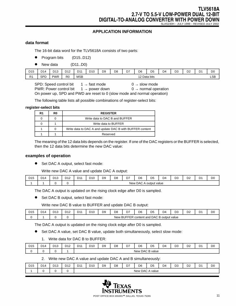
data format
The 16-bit data word for the TLV5618A consists of two parts:
Program bits (D15..D12)
New data (D11..D0)
D15 D14 D13 D12 D11 D10 D9 D8 D7 D6 D5 D4 D3 D2 D1 D0
R1 SPD PWR R0 MSB 12 Data bits LSB
SPD: Speed control bit 1 → fast mode 0 → slow modePWR: Power control bit 1 → power down 0 → normal operationOn power up, SPD and PWD are reset to 0 (slow mode and normal operation)
The following table lists all possible combinations of register-select bits:
register-select bitsR1 R0 REGISTER
0 0 Write data to DAC B and BUFFER
0 1 Write data to BUFFER
1 0 Write data to DAC A and update DAC B with BUFFER content
1 1 Reserved
The meaning of the 12 data bits depends on the register. If one of the DAC registers or the BUFFER is selected,then the 12 data bits determine the new DAC value:
examples of operation
Set DAC A output, select fast mode:
Write new DAC A value and update DAC A output:
D15 D14 D13 D12 D11 D10 D9 D8 D7 D6 D5 D4 D3 D2 D1 D0
1 1 0 0 New DAC A output value
The DAC A output is updated on the rising clock edge after D0 is sampled.
Set DAC B output, select fast mode:
Write new DAC B value to BUFFER and update DAC B output:
D15 D14 D13 D12 D11 D10 D9 D8 D7 D6 D5 D4 D3 D2 D1 D0
0 1 0 0 New BUFFER content and DAC B output value
The DAC A output is updated on the rising clock edge after D0 is sampled.
Set DAC A value, set DAC B value, update both simultaneously, select slow mode:
1. Write data for DAC B to BUFFER:
D15 D14 D13 D12 D11 D10 D9 D8 D7 D6 D5 D4 D3 D2 D1 D0
0 0 0 1 New DAC B value
2. Write new DAC A value and update DAC A and B simultaneously:
D15 D14 D13 D12 D11 D10 D9 D8 D7 D6 D5 D4 D3 D2 D1 D0
1 0 0 0 New DAC A value
TLV5618A2.7-V TO 5.5-V LOW-POWER DUAL 12-BITDIGITAL-TO-ANALOG CONVERTER WITH POWER DOWNSLAS230H – JULY 1999 – REVISED JULY 2002
12 POST OFFICE BOX 655303 • DALLAS, TEXAS 75265
APPLICATION INFORMATION
examples of operation (continued)
Both outputs are updated on the rising clock edge after D0 from the DAC A data word is sampled.
Set power-down mode:
D15 D14 D13 D12 D11 D10 D9 D8 D7 D6 D5 D4 D3 D2 D1 D0
X X 1 X X X X X X X X X X X X X
X = Don’t care
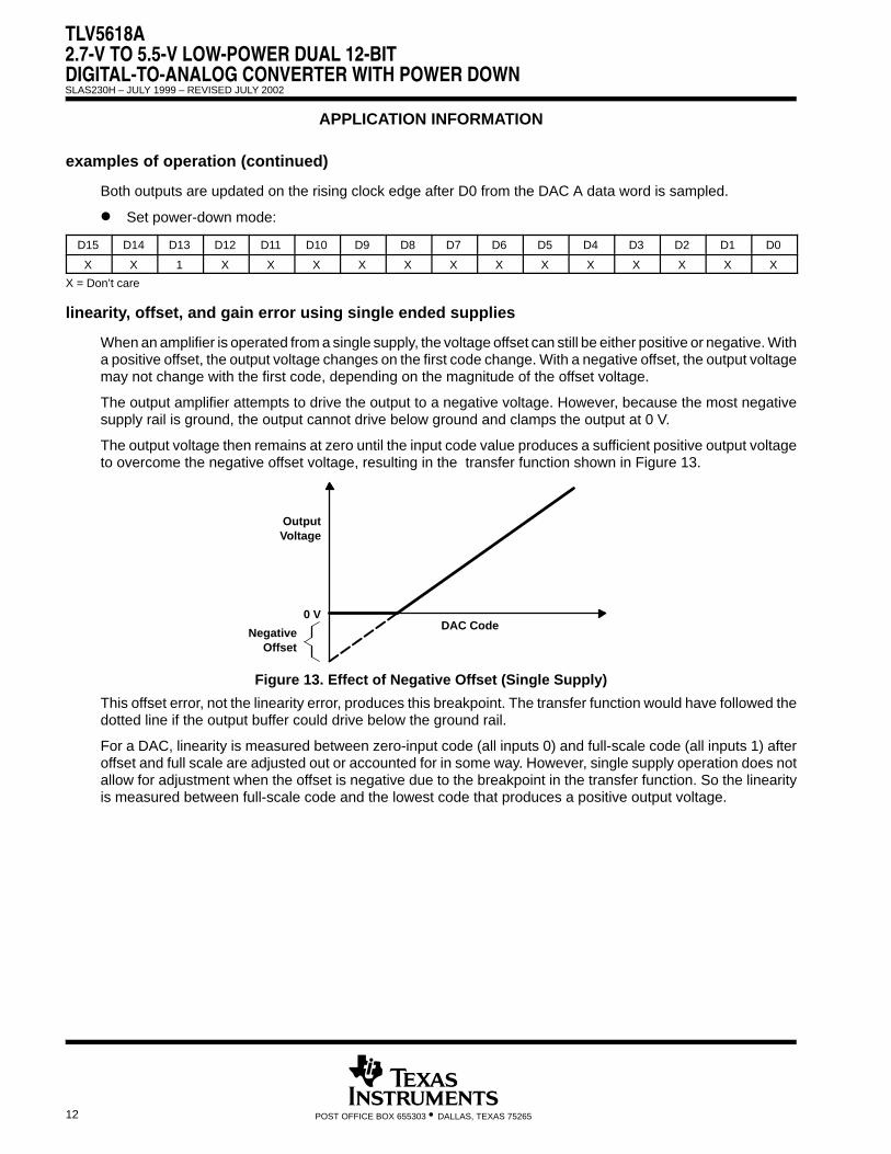
linearity, offset, and gain error using single ended supplies
When an amplifier is operated from a single supply, the voltage offset can still be either positive or negative. Witha positive offset, the output voltage changes on the first code change. With a negative offset, the output voltagemay not change with the first code, depending on the magnitude of the offset voltage.
The output amplifier attempts to drive the output to a negative voltage. However, because the most negativesupply rail is ground, the output cannot drive below ground and clamps the output at 0 V.
The output voltage then remains at zero until the input code value produces a sufficient positive output voltageto overcome the negative offset voltage, resulting in the transfer function shown in Figure 13.
DAC Code
OutputVoltage
0 V
NegativeOffset
Figure 13. Effect of Negative Offset (Single Supply)
This offset error, not the linearity error, produces this breakpoint. The transfer function would have followed thedotted line if the output buffer could drive below the ground rail.
For a DAC, linearity is measured between zero-input code (all inputs 0) and full-scale code (all inputs 1) afteroffset and full scale are adjusted out or accounted for in some way. However, single supply operation does notallow for adjustment when the offset is negative due to the breakpoint in the transfer function. So the linearityis measured between full-scale code and the lowest code that produces a positive output voltage.
TLV5618A2.7-V TO 5.5-V LOW-POWER DUAL 12-BIT
DIGITAL-TO-ANALOG CONVERTER WITH POWER DOWNSLAS230H – JULY 1999 – REVISED JULY 2002
13POST OFFICE BOX 655303 • DALLAS, TEXAS 75265
APPLICATION INFORMATION
definitions of specifications and terminology
integral nonlinearity (INL)
The relative accuracy or integral nonlinearity (INL), sometimes referred to as linearity error, is the maximumdeviation of the output from the line between zero and full scale excluding the effects of zero code and full-scaleerrors.
differential nonlinearity (DNL)
The differential nonlinearity (DNL), sometimes referred to as differential error, is the difference between themeasured and ideal 1 LSB amplitude change of any two adjacent codes. Monotonic means the output voltagechanges in the same direction (or remains constant) as a change in the digital input code.
zero-scale error (EZS)
Zero-scale error is defined as the deviation of the output from 0 V at a digital input value of 0.
gain error (EG)
Gain error is the error in slope of the DAC transfer function.
total harmonic distortion (THD)
THD is the ratio of the rms value of the first six harmonic components to the value of the fundamental signal.The value for THD is expressed in decibels.
signal-to-noise ratio + distortion (S/N+D)
S/N+D is the ratio of the rms value of the output signal to the rms sum of all other spectral components belowthe Nyquist frequency, including harmonics but excluding dc. The value for S/N+D is expressed in decibels.
spurious free dynamic range (SFDR)
Spurious free dynamic range is the difference between the rms value of the output signal and the rms value ofthe largest spurious signal within a specified bandwidth. The value for SFDR is expressed in decibels.
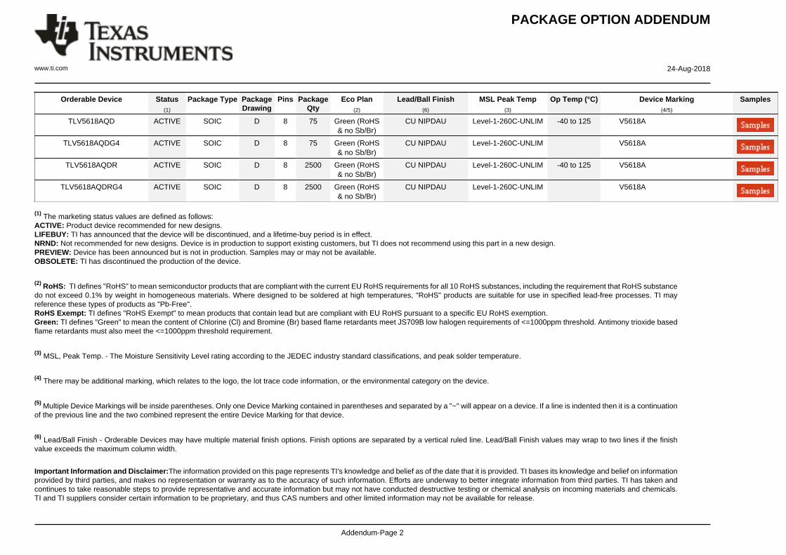
PACKAGE OPTION ADDENDUM
www.ti.com 24-Aug-2018
Addendum-Page 1
PACKAGING INFORMATION
Orderable Device Status(1)
Package Type PackageDrawing
Pins PackageQty
Eco Plan(2)
Lead/Ball Finish(6)
MSL Peak Temp(3)
Op Temp (°C) Device Marking(4/5)
Samples
5962-9955701Q2A ACTIVE LCCC FK 20 1 TBD POST-PLATE N / A for Pkg Type -55 to 125 5962-9955701Q2ATLV5618AMFKB
5962-9955701QPA ACTIVE CDIP JG 8 1 TBD A42 N / A for Pkg Type -55 to 125 9955701QPATLV5618AM
TLV5618ACD ACTIVE SOIC D 8 75 Green (RoHS& no Sb/Br)
CU NIPDAU Level-1-260C-UNLIM 0 to 70 TV5618
TLV5618ACDG4 ACTIVE SOIC D 8 75 Green (RoHS& no Sb/Br)
CU NIPDAU Level-1-260C-UNLIM 0 to 70 TV5618
TLV5618ACDR ACTIVE SOIC D 8 2500 Green (RoHS& no Sb/Br)
CU NIPDAU Level-1-260C-UNLIM 0 to 70 TV5618
TLV5618ACDRG4 ACTIVE SOIC D 8 2500 Green (RoHS& no Sb/Br)
CU NIPDAU Level-1-260C-UNLIM 0 to 70 TV5618
TLV5618ACP ACTIVE PDIP P 8 50 Pb-Free(RoHS)
CU NIPDAU N / A for Pkg Type 0 to 70 TLV5618AC
TLV5618AID ACTIVE SOIC D 8 75 Green (RoHS& no Sb/Br)
CU NIPDAU Level-1-260C-UNLIM -40 to 85 TY5618
TLV5618AIDG4 ACTIVE SOIC D 8 75 Green (RoHS& no Sb/Br)
CU NIPDAU Level-1-260C-UNLIM -40 to 85 TY5618
TLV5618AIDR ACTIVE SOIC D 8 2500 Green (RoHS& no Sb/Br)
CU NIPDAU Level-1-260C-UNLIM -40 to 85 TY5618
TLV5618AIP ACTIVE PDIP P 8 50 Pb-Free(RoHS)
CU NIPDAU N / A for Pkg Type -40 to 85 TLV5618AI
TLV5618AIPE4 ACTIVE PDIP P 8 50 Pb-Free(RoHS)
CU NIPDAU N / A for Pkg Type -40 to 85 TLV5618AI
TLV5618AMFKB ACTIVE LCCC FK 20 1 TBD POST-PLATE N / A for Pkg Type -55 to 125 5962-9955701Q2ATLV5618AMFKB
TLV5618AMJG ACTIVE CDIP JG 8 1 TBD A42 N / A for Pkg Type -55 to 125 TLV5618AMJG
TLV5618AMJGB ACTIVE CDIP JG 8 1 TBD A42 N / A for Pkg Type -55 to 125 9955701QPATLV5618AM
PACKAGE OPTION ADDENDUM
www.ti.com 24-Aug-2018
Addendum-Page 2
Orderable Device Status(1)
Package Type PackageDrawing
Pins PackageQty
Eco Plan(2)
Lead/Ball Finish(6)
MSL Peak Temp(3)
Op Temp (°C) Device Marking(4/5)
Samples
TLV5618AQD ACTIVE SOIC D 8 75 Green (RoHS& no Sb/Br)
CU NIPDAU Level-1-260C-UNLIM -40 to 125 V5618A
TLV5618AQDG4 ACTIVE SOIC D 8 75 Green (RoHS& no Sb/Br)
CU NIPDAU Level-1-260C-UNLIM V5618A
TLV5618AQDR ACTIVE SOIC D 8 2500 Green (RoHS& no Sb/Br)
CU NIPDAU Level-1-260C-UNLIM -40 to 125 V5618A
TLV5618AQDRG4 ACTIVE SOIC D 8 2500 Green (RoHS& no Sb/Br)
CU NIPDAU Level-1-260C-UNLIM V5618A
(1) The marketing status values are defined as follows:ACTIVE: Product device recommended for new designs.LIFEBUY: TI has announced that the device will be discontinued, and a lifetime-buy period is in effect.NRND: Not recommended for new designs. Device is in production to support existing customers, but TI does not recommend using this part in a new design.PREVIEW: Device has been announced but is not in production. Samples may or may not be available.OBSOLETE: TI has discontinued the production of the device.
(2) RoHS: TI defines "RoHS" to mean semiconductor products that are compliant with the current EU RoHS requirements for all 10 RoHS substances, including the requirement that RoHS substancedo not exceed 0.1% by weight in homogeneous materials. Where designed to be soldered at high temperatures, "RoHS" products are suitable for use in specified lead-free processes. TI mayreference these types of products as "Pb-Free".RoHS Exempt: TI defines "RoHS Exempt" to mean products that contain lead but are compliant with EU RoHS pursuant to a specific EU RoHS exemption.Green: TI defines "Green" to mean the content of Chlorine (Cl) and Bromine (Br) based flame retardants meet JS709B low halogen requirements of <=1000ppm threshold. Antimony trioxide basedflame retardants must also meet the <=1000ppm threshold requirement.
(3) MSL, Peak Temp. - The Moisture Sensitivity Level rating according to the JEDEC industry standard classifications, and peak solder temperature.
(4) There may be additional marking, which relates to the logo, the lot trace code information, or the environmental category on the device.
(5) Multiple Device Markings will be inside parentheses. Only one Device Marking contained in parentheses and separated by a "~" will appear on a device. If a line is indented then it is a continuationof the previous line and the two combined represent the entire Device Marking for that device.
(6) Lead/Ball Finish - Orderable Devices may have multiple material finish options. Finish options are separated by a vertical ruled line. Lead/Ball Finish values may wrap to two lines if the finishvalue exceeds the maximum column width.
Important Information and Disclaimer:The information provided on this page represents TI's knowledge and belief as of the date that it is provided. TI bases its knowledge and belief on informationprovided by third parties, and makes no representation or warranty as to the accuracy of such information. Efforts are underway to better integrate information from third parties. TI has taken andcontinues to take reasonable steps to provide representative and accurate information but may not have conducted destructive testing or chemical analysis on incoming materials and chemicals.TI and TI suppliers consider certain information to be proprietary, and thus CAS numbers and other limited information may not be available for release.
PACKAGE OPTION ADDENDUM
www.ti.com 24-Aug-2018
Addendum-Page 3
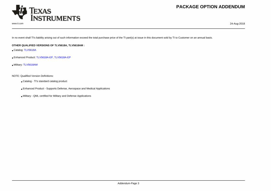
In no event shall TI's liability arising out of such information exceed the total purchase price of the TI part(s) at issue in this document sold by TI to Customer on an annual basis.
OTHER QUALIFIED VERSIONS OF TLV5618A, TLV5618AM :
• Catalog: TLV5618A
• Enhanced Product: TLV5618A-EP, TLV5618A-EP
• Military: TLV5618AM
NOTE: Qualified Version Definitions:
• Catalog - TI's standard catalog product
• Enhanced Product - Supports Defense, Aerospace and Medical Applications
• Military - QML certified for Military and Defense Applications
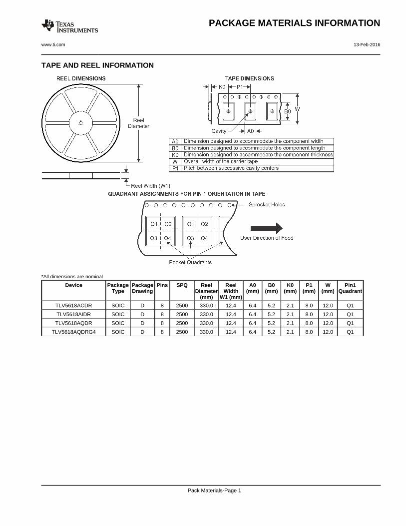
TAPE AND REEL INFORMATION
*All dimensions are nominal
Device PackageType
PackageDrawing
Pins SPQ ReelDiameter
(mm)
ReelWidth
W1 (mm)
A0(mm)
B0(mm)
K0(mm)
P1(mm)
W(mm)
Pin1Quadrant
TLV5618ACDR SOIC D 8 2500 330.0 12.4 6.4 5.2 2.1 8.0 12.0 Q1
TLV5618AIDR SOIC D 8 2500 330.0 12.4 6.4 5.2 2.1 8.0 12.0 Q1
TLV5618AQDR SOIC D 8 2500 330.0 12.4 6.4 5.2 2.1 8.0 12.0 Q1
TLV5618AQDRG4 SOIC D 8 2500 330.0 12.4 6.4 5.2 2.1 8.0 12.0 Q1
PACKAGE MATERIALS INFORMATION
www.ti.com 13-Feb-2016
Pack Materials-Page 1
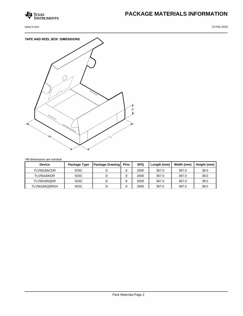
*All dimensions are nominal
Device Package Type Package Drawing Pins SPQ Length (mm) Width (mm) Height (mm)
TLV5618ACDR SOIC D 8 2500 367.0 367.0 38.0
TLV5618AIDR SOIC D 8 2500 367.0 367.0 38.0
TLV5618AQDR SOIC D 8 2500 367.0 367.0 38.0
TLV5618AQDRG4 SOIC D 8 2500 367.0 367.0 38.0
PACKAGE MATERIALS INFORMATION
www.ti.com 13-Feb-2016
Pack Materials-Page 2
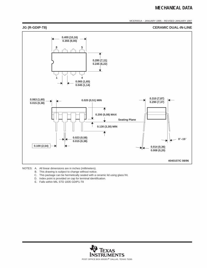
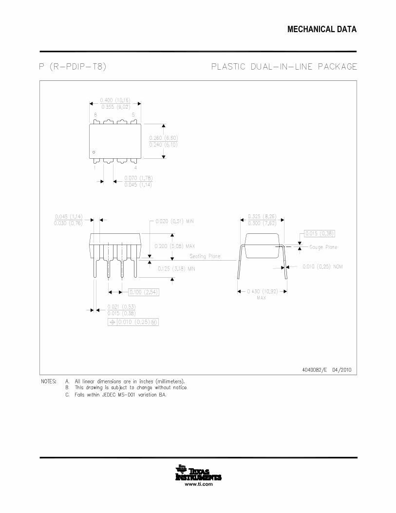
MECHANICAL DATA
MCER001A – JANUARY 1995 – REVISED JANUARY 1997
POST OFFICE BOX 655303 • DALLAS, TEXAS 75265
JG (R-GDIP-T8) CERAMIC DUAL-IN-LINE
0.310 (7,87)0.290 (7,37)
0.014 (0,36)0.008 (0,20)
Seating Plane
4040107/C 08/96
5
40.065 (1,65)0.045 (1,14)
8
1
0.020 (0,51) MIN
0.400 (10,16)0.355 (9,00)
0.015 (0,38)0.023 (0,58)
0.063 (1,60)0.015 (0,38)
0.200 (5,08) MAX
0.130 (3,30) MIN
0.245 (6,22)0.280 (7,11)
0.100 (2,54)
0°–15°
NOTES: A. All linear dimensions are in inches (millimeters).B. This drawing is subject to change without notice.C. This package can be hermetically sealed with a ceramic lid using glass frit.D. Index point is provided on cap for terminal identification.E. Falls within MIL STD 1835 GDIP1-T8
IMPORTANT NOTICE
Texas Instruments Incorporated (TI) reserves the right to make corrections, enhancements, improvements and other changes to itssemiconductor products and services per JESD46, latest issue, and to discontinue any product or service per JESD48, latest issue. Buyersshould obtain the latest relevant information before placing orders and should verify that such information is current and complete.TI’s published terms of sale for semiconductor products (http://www.ti.com/sc/docs/stdterms.htm) apply to the sale of packaged integratedcircuit products that TI has qualified and released to market. Additional terms may apply to the use or sale of other types of TI products andservices.Reproduction of significant portions of TI information in TI data sheets is permissible only if reproduction is without alteration and isaccompanied by all associated warranties, conditions, limitations, and notices. TI is not responsible or liable for such reproduceddocumentation. Information of third parties may be subject to additional restrictions. Resale of TI products or services with statementsdifferent from or beyond the parameters stated by TI for that product or service voids all express and any implied warranties for theassociated TI product or service and is an unfair and deceptive business practice. TI is not responsible or liable for any such statements.Buyers and others who are developing systems that incorporate TI products (collectively, “Designers”) understand and agree that Designersremain responsible for using their independent analysis, evaluation and judgment in designing their applications and that Designers havefull and exclusive responsibility to assure the safety of Designers' applications and compliance of their applications (and of all TI productsused in or for Designers’ applications) with all applicable regulations, laws and other applicable requirements. Designer represents that, withrespect to their applications, Designer has all the necessary expertise to create and implement safeguards that (1) anticipate dangerousconsequences of failures, (2) monitor failures and their consequences, and (3) lessen the likelihood of failures that might cause harm andtake appropriate actions. Designer agrees that prior to using or distributing any applications that include TI products, Designer willthoroughly test such applications and the functionality of such TI products as used in such applications.TI’s provision of technical, application or other design advice, quality characterization, reliability data or other services or information,including, but not limited to, reference designs and materials relating to evaluation modules, (collectively, “TI Resources”) are intended toassist designers who are developing applications that incorporate TI products; by downloading, accessing or using TI Resources in anyway, Designer (individually or, if Designer is acting on behalf of a company, Designer’s company) agrees to use any particular TI Resourcesolely for this purpose and subject to the terms of this Notice.TI’s provision of TI Resources does not expand or otherwise alter TI’s applicable published warranties or warranty disclaimers for TIproducts, and no additional obligations or liabilities arise from TI providing such TI Resources. TI reserves the right to make corrections,enhancements, improvements and other changes to its TI Resources. TI has not conducted any testing other than that specificallydescribed in the published documentation for a particular TI Resource.Designer is authorized to use, copy and modify any individual TI Resource only in connection with the development of applications thatinclude the TI product(s) identified in such TI Resource. NO OTHER LICENSE, EXPRESS OR IMPLIED, BY ESTOPPEL OR OTHERWISETO ANY OTHER TI INTELLECTUAL PROPERTY RIGHT, AND NO LICENSE TO ANY TECHNOLOGY OR INTELLECTUAL PROPERTYRIGHT OF TI OR ANY THIRD PARTY IS GRANTED HEREIN, including but not limited to any patent right, copyright, mask work right, orother intellectual property right relating to any combination, machine, or process in which TI products or services are used. Informationregarding or referencing third-party products or services does not constitute a license to use such products or services, or a warranty orendorsement thereof. Use of TI Resources may require a license from a third party under the patents or other intellectual property of thethird party, or a license from TI under the patents or other intellectual property of TI.TI RESOURCES ARE PROVIDED “AS IS” AND WITH ALL FAULTS. TI DISCLAIMS ALL OTHER WARRANTIES ORREPRESENTATIONS, EXPRESS OR IMPLIED, REGARDING RESOURCES OR USE THEREOF, INCLUDING BUT NOT LIMITED TOACCURACY OR COMPLETENESS, TITLE, ANY EPIDEMIC FAILURE WARRANTY AND ANY IMPLIED WARRANTIES OFMERCHANTABILITY, FITNESS FOR A PARTICULAR PURPOSE, AND NON-INFRINGEMENT OF ANY THIRD PARTY INTELLECTUALPROPERTY RIGHTS. TI SHALL NOT BE LIABLE FOR AND SHALL NOT DEFEND OR INDEMNIFY DESIGNER AGAINST ANY CLAIM,INCLUDING BUT NOT LIMITED TO ANY INFRINGEMENT CLAIM THAT RELATES TO OR IS BASED ON ANY COMBINATION OFPRODUCTS EVEN IF DESCRIBED IN TI RESOURCES OR OTHERWISE. IN NO EVENT SHALL TI BE LIABLE FOR ANY ACTUAL,DIRECT, SPECIAL, COLLATERAL, INDIRECT, PUNITIVE, INCIDENTAL, CONSEQUENTIAL OR EXEMPLARY DAMAGES INCONNECTION WITH OR ARISING OUT OF TI RESOURCES OR USE THEREOF, AND REGARDLESS OF WHETHER TI HAS BEENADVISED OF THE POSSIBILITY OF SUCH DAMAGES.Unless TI has explicitly designated an individual product as meeting the requirements of a particular industry standard (e.g., ISO/TS 16949and ISO 26262), TI is not responsible for any failure to meet such industry standard requirements.Where TI specifically promotes products as facilitating functional safety or as compliant with industry functional safety standards, suchproducts are intended to help enable customers to design and create their own applications that meet applicable functional safety standardsand requirements. Using products in an application does not by itself establish any safety features in the application. Designers mustensure compliance with safety-related requirements and standards applicable to their applications. Designer may not use any TI products inlife-critical medical equipment unless authorized officers of the parties have executed a special contract specifically governing such use.Life-critical medical equipment is medical equipment where failure of such equipment would cause serious bodily injury or death (e.g., lifesupport, pacemakers, defibrillators, heart pumps, neurostimulators, and implantables). Such equipment includes, without limitation, allmedical devices identified by the U.S. Food and Drug Administration as Class III devices and equivalent classifications outside the U.S.TI may expressly designate certain products as completing a particular qualification (e.g., Q100, Military Grade, or Enhanced Product).Designers agree that it has the necessary expertise to select the product with the appropriate qualification designation for their applicationsand that proper product selection is at Designers’ own risk. Designers are solely responsible for compliance with all legal and regulatoryrequirements in connection with such selection.Designer will fully indemnify TI and its representatives against any damages, costs, losses, and/or liabilities arising out of Designer’s non-compliance with the terms and provisions of this Notice.
Mailing Address: Texas Instruments, Post Office Box 655303, Dallas, Texas 75265Copyright © 2018, Texas Instruments Incorporated