Embed Size (px)
Citation preview

Rev. 1.5 3/14 Copyright © 2014 by Silicon Laboratories Si823x
Si823x
0.5 AND 4.0 AMP ISODRIVERS (2.5 AND 5 KVRMS)
Features
Applications
Safety Approval
Description
The Si823x isolated driver family combines two independent, isolateddrivers into a single package. The Si8230/1/3/4 are high-side/low-sidedrivers, and the Si8232/5/6/7/8 are dual drivers. Versions with peakoutput currents of 0.5 A (Si8230/1/2/7) and 4.0 A (Si8233/4/5/6/8) areavailable. All drivers operate with a maximum supply voltage of 24 V.
The Si823x drivers utilize Silicon Labs' proprietary silicon isolationtechnology, which provides up to 5 kVRMS withstand voltage per UL1577and fast 60 ns propagation times. Driver outputs can be grounded to thesame or separate grounds or connected to a positive or negative voltage.The TTL level compatible inputs with >400 mV hysteresis are available inindividual control input (Si8230/2/3/5/6/7/8) or PWM input (Si8231/4)configurations. High integration, low propagation delay, small installedsize, flexibility, and cost-effectiveness make the Si823x family ideal for awide range of isolated MOSFET/IGBT gate drive applications.
Two completely isolated drivers in one packageUp to 5 kVRMS input-to-output
isolationUp to 1500 VDC peak driver-to-
driver differential voltage
HS/LS and dual driver versions
Up to 8 MHz switching frequency
0.5 A peak output (Si8230/1/2/7)
4.0 A peak output (Si8233/4/5/6/8)
High electromagnetic immunity
60 ns propagation delay (max)
Independent HS and LS inputs or PWM input versions
Transient immunity >45 kV/µs
Overlap protection and programmable dead time
AEC-Q100 qualification Wide operating range
–40 to +125 °C
RoHS-compliant packagesSOIC-16 wide bodySOIC-16 narrow bodyLGA-14
Power delivery systems
Motor control systems
Isolated dc-dc power supplies
Lighting control systems
Plasma displays
Solar and industrial inverters
UL 1577 recognizedUp to 5000 Vrms for 1 minute
CSA component notice 5A approvalIEC 60950-1, 61010-1, 60601-1
(reinforced insulation)
VDE certification conformityIEC 60747-5-5 (VDE 0884 Part 5)EN 60950-1 (reinforced
insulation)
CQC certification approvalGB4943.1
Ordering Information:
See page 39.

Si823x
2 Rev. 1.5

Si823x
Rev. 1.5 3
TABLE OF CONTENTS
Section Page
1. Top-Level Block Diagrams . . . . . . . . . . . . . . . . . . . . . . . . . . . . . . . . . . . . . . . . . . . . . . . . .42. Electrical Specifications . . . . . . . . . . . . . . . . . . . . . . . . . . . . . . . . . . . . . . . . . . . . . . . . . . .6
2.1. Test Circuits . . . . . . . . . . . . . . . . . . . . . . . . . . . . . . . . . . . . . . . . . . . . . . . . . . . . . . . .93. Functional Description . . . . . . . . . . . . . . . . . . . . . . . . . . . . . . . . . . . . . . . . . . . . . . . . . . .16
3.1. Typical Operating Characteristics (0.5 Amp) . . . . . . . . . . . . . . . . . . . . . . . . . . . . . .173.2. Typical Operating Characteristics (4.0 Amp) . . . . . . . . . . . . . . . . . . . . . . . . . . . . . .193.3. Family Overview and Logic Operation During Startup . . . . . . . . . . . . . . . . . . . . . . .213.4. Power Supply Connections . . . . . . . . . . . . . . . . . . . . . . . . . . . . . . . . . . . . . . . . . . . .233.5. Power Dissipation Considerations . . . . . . . . . . . . . . . . . . . . . . . . . . . . . . . . . . . . . .233.6. Layout Considerations . . . . . . . . . . . . . . . . . . . . . . . . . . . . . . . . . . . . . . . . . . . . . . .263.7. Undervoltage Lockout Operation . . . . . . . . . . . . . . . . . . . . . . . . . . . . . . . . . . . . . . .263.8. Programmable Dead Time and Overlap Protection . . . . . . . . . . . . . . . . . . . . . . . . .28
4. Applications . . . . . . . . . . . . . . . . . . . . . . . . . . . . . . . . . . . . . . . . . . . . . . . . . . . . . . . . . . . .304.1. High-Side/Low-Side Driver . . . . . . . . . . . . . . . . . . . . . . . . . . . . . . . . . . . . . . . . . . . .304.2. Dual Driver . . . . . . . . . . . . . . . . . . . . . . . . . . . . . . . . . . . . . . . . . . . . . . . . . . . . . . . .314.3. Dual Driver with Thermally Enhanced Package (Si8236) . . . . . . . . . . . . . . . . . . . . .31
5. Pin Descriptions . . . . . . . . . . . . . . . . . . . . . . . . . . . . . . . . . . . . . . . . . . . . . . . . . . . . . . . . .326. Ordering Guide . . . . . . . . . . . . . . . . . . . . . . . . . . . . . . . . . . . . . . . . . . . . . . . . . . . . . . . . . .397. Package Outline: 16-Pin Wide Body SOIC . . . . . . . . . . . . . . . . . . . . . . . . . . . . . . . . . . . .438. Land Pattern: 16-Pin Wide Body SOIC . . . . . . . . . . . . . . . . . . . . . . . . . . . . . . . . . . . . . . .459. Package Outline: 16-Pin Narrow Body SOIC . . . . . . . . . . . . . . . . . . . . . . . . . . . . . . . . . .4610. Land Pattern: 16-Pin Narrow Body SOIC . . . . . . . . . . . . . . . . . . . . . . . . . . . . . . . . . . . .4711. Package Outline: 14 LD LGA (5 x 5 mm) . . . . . . . . . . . . . . . . . . . . . . . . . . . . . . . . . . . .4812. Land Pattern: 14 LD LGA . . . . . . . . . . . . . . . . . . . . . . . . . . . . . . . . . . . . . . . . . . . . . . . . .4913. Package Outline: 14 LD LGA with Thermal Pad (5 x 5 mm) . . . . . . . . . . . . . . . . . . . . .5014. Land Pattern: 14 LD LGA with Thermal Pad . . . . . . . . . . . . . . . . . . . . . . . . . . . . . . . . .5115. Top Markings . . . . . . . . . . . . . . . . . . . . . . . . . . . . . . . . . . . . . . . . . . . . . . . . . . . . . . . . . .52
15.1. Si823x Top Marking (16-Pin Wide Body SOIC) . . . . . . . . . . . . . . . . . . . . . . . . . . .5215.2. Top Marking Explanation (16-Pin Wide Body SOIC) . . . . . . . . . . . . . . . . . . . . . . .5215.3. Si823x Top Marking (16-Pin Narrow Body SOIC) . . . . . . . . . . . . . . . . . . . . . . . . . .5315.4. Top Marking Explanation (16-Pin Narrow Body SOIC) . . . . . . . . . . . . . . . . . . . . . .5315.5. Si823x Top Marking (14 LD LGA) . . . . . . . . . . . . . . . . . . . . . . . . . . . . . . . . . . . . . .5415.6. Top Marking Explanation (14 LD LGA) . . . . . . . . . . . . . . . . . . . . . . . . . . . . . . . . . .54
Document Change List . . . . . . . . . . . . . . . . . . . . . . . . . . . . . . . . . . . . . . . . . . . . . . . . . . . . .55Contact Information . . . . . . . . . . . . . . . . . . . . . . . . . . . . . . . . . . . . . . . . . . . . . . . . . . . . . . . .56

Si823x
4 Rev. 1.5
1. Top-Level Block Diagrams
Figure 1. Si8230/3 Two-Input High-Side/Low-Side Isolated Drivers
Figure 2. Si8231/4 Single-Input High-Side/Low-Side Isolated Drivers
Si8230/3
UVLO
UVLO
GNDI
VIB
VDDI
VIA VDDA
VOA
GNDA
VOB
VDDI
VDDI
ISO
LA
TIO
N
VDDIVDDB
GNDBDISABLE
ISO
LA
TIO
N
UVLO
DT CONTROL &
OVERLAP PROTECTION
DT
Si8231/4
UVLO
UVLO
GNDI
VDDI
PWM VDDA
VOA
GNDA
VOB
VDDI
VDDI
ISO
LA
TIO
N
VDDIVDDB
GNDBDISABLE
ISO
LA
TIO
N
UVLO
DT CONTROL&
OVERLAP PROTECTION
DT
LPWM
LPWM

Si823x
Rev. 1.5 5
Figure 3. Si8232/5/6/7/8 Dual Isolated Drivers
Si8232/5/6/7/8
UVLO
VDDA
VOA
GNDA
VOB
VDDI
ISO
LA
TIO
N
VDDIVDDB
GNDB
UVLO
VIA
ISO
LA
TIO
N
UVLO
GNDI
VIB
VDDI
VDDI
DISABLE

Si823x
6 Rev. 1.5
2. Electrical Specifications
Table 1. Electrical Characteristics1
2.7 V < VDDI < 5.5 V, VDDA = VDDB = 12 V or 15 V. TA = –40 to +125 °C. Typical specs at 25 °C
Parameter Symbol Test Condition Min Typ Max Unit
DC Specifications
Input-side Power SupplyVoltage
VDDISi8230/1/2/3/4/5/6
Si8237/84.52.7
——
5.55.5
V
Driver Supply Voltage VDDA, VDDBVoltage between VDDA and
GNDA, and VDDB and GNDB(See “6. Ordering Guide” )
6.5 — 24 V
Input Supply QuiescentCurrent
IDDI(Q)Si8230/2/3/5/6/7/8 — 2 3 mA
Si8231/4 — 3.5 5 mA
Output Supply QuiescentCurrent
IDDA(Q), IDDB(Q)
Current per channel — — 3.0 mA
Input Supply Active Current IDDI Input freq = 500 kHz, no load — 3.5 — mA
Output Supply Active CurrentIDDAIDDB
Current per channel withInput freq = 500 kHz, no load
— 6 — mA
Input Pin Leakage CurrentIVIA, IVIB,
IPWM–10 — +10 µA dc
Input Pin Leakage Current IDISABLE –10 — +10 µA dc
Logic High Input Threshold VIH 2.0 — — V
Logic Low Input Threshold VIL — — 0.8 V
Input Hysteresis VIHYST Si8230/1/2/3/4/5/6/7/8 400 450 — mV
Logic High Output VoltageVOAH, VOBH
IOA, IOB = –1 mA(VDDA /VDDB) — 0.04
— — V
Logic Low Output Voltage VOAL, VOBL IOA, IOB = 1 mA — — 0.04 V
Output Short-Circuit Pulsed Sink Current
IOA(SCL), IOB(SCL)
Si8230/1/2/7, Figure 4 — 0.5 — A
Si8233/4/5/6/8, Figure 4 — 4.0 — A
Output Short-Circuit Pulsed Source Current
IOA(SCH), IOB(SCH)
Si8230/1/2/7, Figure 5 — 0.25 — A
Si8233/4/5/6/8, Figure 5 — 2.0 — A
Output Sink Resistance RON(SINK)
Si8230/1/2/7 — 5.0 —
Si8233/4/5/6/8 — 1.0 —
Notes:1. VDDA = VDDB = 12 V for 5, 8, and 10 V UVLO devices; VDDA = VDDB = 15 V for 12.5 V UVLO devices.2. TDD is the minimum overlap time without triggering overlap protection (Si8230/1/3/4 only).3. The largest RDT resistor that can be used is 220 k..

Si823x
Rev. 1.5 7
Output Source Resistance RON(SOURCE)
Si8230/1/2/7 — 15 —
Si8233/4/5/6/8 — 2.7 —
VDDI Undervoltage Threshold VDDIUV+VDDI rising
(Si8230/1/2/3/4/5/6)3.60 4.0 4.45 V
VDDI Undervoltage Threshold VDDIUV–VDDI falling
(Si8230/1/2/3/4/5/6)3.30 3.70 4.15 V
VDDI Lockout Hysteresis VDDIHYS (Si8230/1/2/3/4/5/6) — 250 — mV
VDDI Undervoltage Threshold VDDIUV+ VDDI rising (Si8237/8) 2.15 2.3 2.5 V
VDDI Undervoltage Threshold VDDIUV– VDDI falling (Si8237/8) 2.10 2.22 2.40 V
VDDI Lockout Hysteresis VDDIHYS (Si8237/8) — 75 — mV
VDDA, VDDB Undervoltage Threshold
VDDAUV+, VDDBUV+
VDDA, VDDB rising
5 V Threshold See Figure 37 on page 27. 5.20 5.80 6.30 V
8 V Threshold See Figure 38 on page 27. 7.50 8.60 9.40 V
10 V Threshold See Figure 39 on page 27. 9.60 11.1 12.2 V
12.5 V Threshold See Figure 40 on page 27. 12.4 13.8 14.8 V
VDDA, VDDB Undervoltage Threshold
VDDAUV–, VDDBUV–
VDDA, VDDB falling
5 V Threshold See Figure 37 on page 27. 4.90 5.52 6.0 V
8 V Threshold See Figure 38 on page 27. 7.20 8.10 8.70 V
10 V Threshold See Figure 39 on page 27. 9.40 10.1 10.9 V
12.5 V Threshold See Figure 40 on page 27. 11.6 12.8 13.8 V
VDDA, VDDB Lockout Hysteresis
VDDAHYS, VDDBHYS
UVLO voltage = 5 V — 280 — mV
VDDA, VDDB Lockout Hysteresis
VDDAHYS, VDDBHYS
UVLO voltage = 8 V — 600 — mV
VDDA, VDDB Lockout Hysteresis
VDDAHYS, VDDBHYS
UVLO voltage = 10 V or 12.5 V — 1000 — mV
Table 1. Electrical Characteristics1 (Continued)2.7 V < VDDI < 5.5 V, VDDA = VDDB = 12 V or 15 V. TA = –40 to +125 °C. Typical specs at 25 °C
Parameter Symbol Test Condition Min Typ Max Unit
Notes:1. VDDA = VDDB = 12 V for 5, 8, and 10 V UVLO devices; VDDA = VDDB = 15 V for 12.5 V UVLO devices.2. TDD is the minimum overlap time without triggering overlap protection (Si8230/1/3/4 only).3. The largest RDT resistor that can be used is 220 k..

Si823x
8 Rev. 1.5
AC Specifications
Minimum Pulse Width — 10 — ns
Propagation Delay tPHL, tPLH CL = 200 pF — 30 60 ns
Pulse Width Distortion|tPLH - tPHL|
PWD — — 5.60 ns
Minimum Overlap Time2 TDD DT = VDDI, No-Connect — 0.4 — ns
Programmed Dead Time3 DTFigure 42, RDT = 100 k — 900 — ns
Figure 42, RDT = 6 k — 70 — ns
Output Rise and Fall Time tR,tFCL = 200 pF (Si8230/1/2/7) — — 20 ns
CL = 200 pF (Si8233/4/5/6/8) — — 12 ns
Shutdown Time fromDisable True
tSD — — 60 ns
Restart Time fromDisable False
tRESTART — — 60 ns
Device Start-up Time tSTARTTime from VDD_ = VDD_UV+
to VOA, VOB = VIA, VIB — — 40 µs
Common ModeTransient Immunity
CMTIVIA, VIB, PWM = VDDI or 0 VVCM = 1500 V (see Figure 6)
20 45 — kV/µs
Table 1. Electrical Characteristics1 (Continued)2.7 V < VDDI < 5.5 V, VDDA = VDDB = 12 V or 15 V. TA = –40 to +125 °C. Typical specs at 25 °C
Parameter Symbol Test Condition Min Typ Max Unit
Notes:1. VDDA = VDDB = 12 V for 5, 8, and 10 V UVLO devices; VDDA = VDDB = 15 V for 12.5 V UVLO devices.2. TDD is the minimum overlap time without triggering overlap protection (Si8230/1/3/4 only).3. The largest RDT resistor that can be used is 220 k..

Si823x
Rev. 1.5 9
2.1. Test CircuitsFigures 4, 5, and 6 depict sink current, source current, and common-mode transient immunity test circuits,respectively.
Figure 4. IOL Sink Current Test Circuit
Figure 5. IOH Source Current Test Circuit
INPUT
1 µF 100 µF
10
RSNS0.1
Si823x
1 µFCER
10 µFEL
VDDA = VDDB = 15 V
IN OUT
VSS
VDD
SCHOTTKY
50 ns
200 ns
Measure
INPUT WAVEFORM
GND
VDDI
VDDI
8 V+_
INPUT
1 µF 100 µF
10
RSNS0.1
Si823x
1 µFCER
10 µFEL
VDDA = VDDB = 15 V
IN OUT
VSS
VDD
50 ns
200 ns
Measure
INPUT WAVEFORM
GND
VDDI
SCHOTTKY
VDDI
5.5 V +_

Si823x
10 Rev. 1.5
Figure 6. Common Mode Transient Immunity Test Circuit
Oscilloscope
5VIsolated Supply
VDDA
VOA
GNDA
12 VSupply
High Voltage Surge Generator
Vcm SurgeOutput
100k
High Voltage Differential
Probe
VDDB
VOB
GNDB
DT
GNDI
VDDI
INPUT
DISABLE
Input SignalSwitch
InputOutput
Isolated Ground
Si823x

Si823x
Rev. 1.5 11
Table 2. Regulatory Information1,2,3,4
CSA
The Si823x is certified under CSA Component Acceptance Notice 5A. For more details, see File 232873.
61010-1: Up to 600 VRMS reinforced insulation working voltage; up to 600 VRMS basic insulation working voltage.
60950-1: Up to 600 VRMS reinforced insulation working voltage; up to 1000 VRMS basic insulation working volt-age.
60601-1: Up to 125 VRMS reinforced insulation working voltage; up to 380 VRMS basic insulation working voltage.
VDE
The Si823x is certified according to IEC 60747-5-5. For more details, see File 5006301-4880-0001.
60747-5-5: Up to 891 Vpeak for basic insulation working voltage.
60950-1: Up to 600 VRMS reinforced insulation working voltage; up to 1000 VRMS basic insulation working volt-age.
UL
The Si823x is certified under UL1577 component recognition program. For more details, see File E257455.
Rated up to 5000 VRMS isolation voltage for basic protection.
CQC
The Si823x is certified under GB4943.1-2011. For more details, see File V2012CQC001041.
Rated up to 600 VRMS reinforced insulation working voltage; up to 1000 VRMS basic insulation working voltage.
Notes:1. Regulatory Certifications apply to 2.5 kVRMS rated devices which are production tested to 3.0 kVRMS for 1 sec.2. Regulatory Certifications apply to 3.75 kVRMS rated devices which are production tested to 4.5 kVRMS for 1 sec.3. Regulatory Certifications apply to 5.0 kVRMS rated devices which are production tested to 6.0 kVRMS for 1 sec.4. For more information, see "6. Ordering Guide" on page 39.

Si823x
12 Rev. 1.5
Table 3. Insulation and Safety-Related Specifications
Parameter SymbolTest
Condition
Value
UnitWBSOIC-165 kVRMS
WBSOIC-16NBSOIC-162.5 kVRMS
14 LD LGA
2.5 kVRMS
14 LD LGA with
Pad1.0 kVRMS
Nominal Air Gap (Clearance)1
L(1O1) 8.0 8.0/4.01 3.5 1.75 mm
Nominal External Tracking (Creepage)1
L(1O2) 8.0 8.0/4.01 3.5 1.75 mm
Minimum Internal Gap (Internal Clearance)
0.014 0.014 0.014 0.014 mm
Tracking Resistance(Proof Tracking Index)
PTI IEC60112 600 600 600 600 V
Erosion Depth ED 0.040 0.019 0.021 0.021 mm
Resistance (Input-Output)2
RIO 1012 1012 1012 1012
Capacitance (Input-Output)2
CIO f = 1 MHz 1.4 1.4 1.4 1.4 pF
Input Capacitance3 CI 4.0 4.0 4.0 4.0 pF
Notes:1. The values in this table correspond to the nominal creepage and clearance values as detailed in “7. Package Outline:
16-Pin Wide Body SOIC” , “9. Package Outline: 16-Pin Narrow Body SOIC” , “11. Package Outline: 14 LD LGA (5 x 5 mm)” , and “13. Package Outline: 14 LD LGA with Thermal Pad (5 x 5 mm)” . VDE certifies the clearance and creepage limits as 4.7 mm minimum for the NB SOIC-16 and 8.5 mm minimum for the WB SOIC-16 package. UL does not impose a clearance and creepage minimum for component level certifications. CSA certifies the clearance and creepage limits as 3.9 mm minimum for the NB SOIC 16 and 7.6 mm minimum for the WB SOIC-16 package.
2. To determine resistance and capacitance, the Si823x is converted into a 2-terminal device. Pins 1–8 (1-7, 14 LD LGA) are shorted together to form the first terminal and pins 9–16 (8-14, 14 LD LGA) are shorted together to form the second terminal. The parameters are then measured between these two terminals.
3. Measured from input pin to ground.
Table 4. IEC 60664-1 (VDE 0884 Part 5) Ratings
Parameter Test Condition
Specification
WB SOIC-16
NB SOIC-16
14 LD LGA
14 LD LGA
with Pad
Basic Isolation Group Material Group I I I I
Installation Classification
Rated Mains Voltages < 150 VRMS I-IV I-IV I-IV I-IV
Rated Mains Voltages < 300 VRMS I-IV I-III I-III I-III
Rated Mains Voltages < 400 VRMS I-III I-II I-II I-II
Rated Mains Voltages < 600 VRMS I-III I-II I-II I-I

Si823x
Rev. 1.5 13
Table 5. IEC 60747-5-5 Insulation Characteristics*
Parameter Symbol Test Condition
Characteristic
UnitWBSOIC-16
NB SOIC-1614 LD LGA
14 LD LGA with Pad
Maximum Working Insulation Voltage
VIORM 891 560 373 V peak
Input to Output Test Voltage VPR
Method b1(VIORM x 1.875 = VPR,
100%Production Test,
tm = 1 sec,Partial Discharge < 5
pC)
1375 1050 700 V peak
Transient Overvoltage VIOTM t = 60 sec 6000 4000 2650 V peak
Pollution Degree (DIN VDE 0110, Table 1)
2 2 2
Insulation Resistance at TS, VIO = 500 V
RS >109 >109 >109
*Note: Maintenance of the safety data is ensured by protective circuits. The Si823x provides a climate classification of 40/125/21.
Table 6. IEC Safety Limiting Values1
Parameter Symbol Test ConditionWB
SOIC-16NB
SOIC-16 14 LD LGA
14 LD LGA with
PadUnit
Case Temperature
TS 150 150 150 150 °C
Safety Input Current
IS
JA = 100 °C/W (WB SOIC-16),105 °C/W (NB SOIC-16, 14 LD LGA),
50 °C/W (14 LD LGA with Pad)VDDI = 5.5 V,
VDDA = VDDB = 24 V,TJ = 150 °C, TA = 25 °C
50 50 50 100 mA
Device Power Dissipation2 PD 1.2 1.2 1.2 1.2 W
Notes:1. Maximum value allowed in the event of a failure. Refer to the thermal derating curve in Figures 7 and 8.2. The Si82xx is tested with VDDI = 5.5 V, VDDA = VDDB = 24 V, TJ = 150 ºC, CL = 100 pF, input 2 MHz 50% duty cycle
square wave.

Si823x
14 Rev. 1.5
Table 7. Thermal Characteristics
Parameter SymbolWB
SOIC-16NB
SOIC-1614 LD LGA
14 LD LGA with
PadUnit
IC Junction-to-Air Thermal Resistance
JA 100 105 105 50 °C/W
Table 8. Absolute Maximum Ratings1
Parameter Symbol Min Typ Max Unit
Storage Temperature2 TSTG –65 — +150 °C
Ambient Temperature under Bias TA –40 — +125 °C
Junction Temperature TJ — — +150 °C
Input-side Supply Voltage VDDI –0.6 — 6.0 V
Driver-side Supply Voltage VDDA, VDDB –0.6 — 30 V
Voltage on any Pin with respect to Ground VIN –0.5 — VDD + 0.5 V
Output Drive Current per Channel IO — — 10 mA
Lead Solder Temperature (10 sec.) — — 260 °C
Maximum Isolation (Input to Output) (1 sec)WB SOIC-16
— — 6500 VRMS
Maximum Isolation (Output to Output) (1 sec)WB SOIC-16
— — 2500 VRMS
Maximum Isolation (Input to Output) (1 sec)NB SOIC-16
— — 4250 VRMS
Maximum Isolation (Output to Output) (1 sec)NB SOIC-16
— — 2500 VRMS
Maximum Isolation (Input to Output) (1 sec)14 LD LGA without Thermal Pad
— — 3850 VRMS
Maximum Isolation (Output to Output) (1 sec)14 LD LGA without Thermal Pad
— — 650 VRMS
Maximum Isolation (Input to Output) (1 sec)14 LD LGA with Thermal Pad
— — 1850 VRMS
Maximum Isolation (Output to Output) (1 sec)14 LD LGA with Thermal Pad
— — 0 VRMS
Notes:1. Permanent device damage may occur if the absolute maximum ratings are exceeded. Functional operation should be
restricted to the conditions as specified in the operational sections of this data sheet. Exposure to absolute maximum rating conditions for extended periods may affect device reliability.
2. VDE certifies storage temperature from –40 to 150 °C.

Si823x
Rev. 1.5 15
Figure 7. WB SOIC-16, NB SOIC-16, 14 LD LGA Thermal Derating Curve, Dependence of Safety Limiting Values with Case Temperature per DIN EN 60747-5-5
Figure 8. 14 LD LGA with Pad Thermal Derating Curve, Dependence of Safety Limiting Values with Case Temperature per DIN EN 60747-5-5
0 20015010050
60
40
20
0
Case Temperature (ºC)
Sa
fety
-Lim
itin
g C
urre
nt (
mA
)
VDDI = 5.5 VVDDA, VDDB = 24 V
10
30
50
0 20015010050
120
80
40
0
Case Temperature (ºC)
Saf
ety-
Lim
iting
Cur
rent
(m
A)
20
60
100VDDI = 5.5 VVDDA, VDDB = 24 V

Si823x
16 Rev. 1.5
3. Functional Description
The operation of an Si823x channel is analogous to that of an optocoupler and gate driver, except an RF carrier ismodulated instead of light. This simple architecture provides a robust isolated data path and requires no specialconsiderations or initialization at start-up. A simplified block diagram for a single Si823x channel is shown inFigure 9.
Figure 9. Simplified Channel Diagram
A channel consists of an RF Transmitter and RF Receiver separated by a semiconductor-based isolation barrier.Referring to the Transmitter, input A modulates the carrier provided by an RF oscillator using on/off keying. TheReceiver contains a demodulator that decodes the input state according to its RF energy content and applies theresult to output B via the output driver. This RF on/off keying scheme is superior to pulse code schemes as itprovides best-in-class noise immunity, low power consumption, and better immunity to magnetic fields. SeeFigure 10 for more details.
Figure 10. Modulation Scheme
RF OSCILLATOR
MODULATOR DEMODULATORA BSemiconductor-Based Isolation
Barrier
Transmitter Receiver
Dead time
control 0.5 to 4 A peak
Gnd
VDD
Driver
Input Signal
Output Signal
Modulation Signal

Si823x
Rev. 1.5 17
3.1. Typical Operating Characteristics (0.5 Amp)The typical performance characteristics depicted in Figures 11 through 22 are for information purposes only. Referto Table 1 on page 6 for actual specification limits.
Figure 11. Rise/Fall Time vs. Supply Voltage
Figure 12. Propagation Delay vs. Supply Voltage
Figure 13. Supply Current vs. Supply Voltage
Figure 14. Supply Current vs. Supply Voltage
Figure 15. Supply Current vs. Temperature
Figure 16. Rise/Fall Time vs. Load
0
2
4
6
8
10
9 12 15 18 21 24
Ris
e/Fa
ll Ti
me
(ns)
VDDA Supply (V)
VDD=12V, 25°CCL = 100 pF
Tfall
Trise
10
15
20
25
30
9 12 15 18 21 24
Prop
agat
ion
Del
ay (n
s)
VDDA Supply (V)
H-L
L-H
VDD=12V, 25°CCL = 100 pF
1
1.5
2
2.5
3
3.5
4
9 14 19 24
VDD
A Su
pply
Cur
rent
(mA)
VDDA Supply Voltage (V)
Duty Cycle = 50%CL = 0 pF1 Channel Switching 1MHz
500kHz
100kHz
50 kHz
0
1
2
3
4
5
6
7
9 14 19 24
VDD
A Su
pply
Cur
rent
(mA)
VDDA Supply Voltage (V)
Duty Cycle = 50%CL = 100 pF1 Channel Switching
1MHz
500kHz
100kHz
50 kHz
1
2
3
4
5
-50 0 50 100
Supp
ly C
urre
nt (m
A)
Temperature (°C)
VDDA = 15V,f = 250kHz, CL = 0 pFDuty Cycle = 50%2 Channels Switching
0
5
10
15
20
25
30
35
40
0.0 0.5 1.0 1.5 2.0
Ris
e/Fa
ll Ti
me
(ns)
Load (nF)
VDD=12V, 25°C
Tfall
Trise

Si823x
18 Rev. 1.5
Figure 17. Propagation Delay vs. Load
Figure 18. Propagation Delay vs. Temperature
Figure 19. Output Sink Current vs. Supply Voltage
Figure 20. Output Source Current vs. Supply Voltage
Figure 21. Output Sink Current vs. Temperature
Figure 22. Output Source Current vs. Temperature
10
15
20
25
30
35
40
45
50
0.0 0.5 1.0 1.5 2.0
Prop
agat
ion
Del
ay (n
s)
Load (nF)
VDD=12V, 25°C
H-L
L-H
10
15
20
25
30
-40 -20 0 20 40 60 80 100 120
Prop
agat
ion
Del
ay (n
s)
Temperature (°C)
VDD=12V, Load = 200pF
H-L
L-H
10 12 14 16 18 20 22 24
VDD=12V, Vout=5V
4
10 15 20 25
VDD=12V, Vout=VDD-5V
7
-40 -10 20 50 80 110
°
VDD=12V, Vout=5V
5
3
5
-40 -10 20 50 80 110
°
VDD=12V, Vout=VDD-5V

Si823x
Rev. 1.5 19
3.2. Typical Operating Characteristics (4.0 Amp)The typical performance characteristics depicted in Figures 23 through 34 are for information purposes only. Referto Table 1 on page 6 for actual specification limits.
Figure 23. Rise/Fall Time vs. Supply Voltage
Figure 24. Propagation Delay vs. Supply Voltage
Figure 25. Supply Current vs. Supply Voltage
Figure 26. Supply Current vs. Supply Voltage
Figure 27. Supply Current vs. Temperature
Figure 28. Rise/Fall Time vs. Load
0
2
4
6
8
10
9 12 15 18 21 24
Ris
e/Fa
ll Ti
me
(ns)
VDDA Supply (V)
VDD=12V, 25°CCL = 100 pF
Tfall
Trise
10
15
20
25
30
9 12 15 18 21 24
Prop
agat
ion
Del
ay (n
s)
VDDA Supply (V)
H-L
L-H
VDD=12V, 25°CCL = 100 pF
0
2
4
6
8
10
12
14
9 14 19 24
VDD
A Su
pply
Cur
rent
(mA)
VDDA Supply Voltage (V)
Duty Cycle = 50%CL = 0 pF1 Channel Switching 1MHz
500kHz
100kHz
50 kHz
0
2
4
6
8
10
12
14
9 14 19 24
VDD
A Su
pply
Cur
rent
(mA)
VDDA Supply Voltage (V)
Duty Cycle = 50%CL = 100 pF1 Channel Switching
1MHz
500kHz
100kHz
50 kHz
0
2
4
6
8
10
-50 0 50 100
Supp
ly C
urre
nt (m
A)
Temperature (°C)
VDDA = 15V,f = 250kHz, CL = 0 pFDuty Cycle = 50%2 Channels Switching
0
5
10
15
20
25
30
35
40
0 1 2 3 4 5 6 7 8 9 10
Ris
e/Fa
ll Ti
me
(ns)
Load (nF)
VDD=12V, 25°C
Tfall
Trise

Si823x
20 Rev. 1.5
Figure 29. Propagation Delay vs. Load
Figure 30. Propagation Delay vs. Temperature
Figure 31. Output Sink Current vs. Supply Voltage
Figure 32. Output Source Current vs. Supply Voltage
Figure 33. Output Sink Current vs. Temperature
Figure 34. Output Source Current vs. Temperature
10
15
20
25
30
35
40
45
50
0 1 2 3 4 5 6 7 8 9 10
Prop
agat
ion
Del
ay (n
s)
Load (nF)
VDD=12V, 25°C
H-L
L-H
10
15
20
25
30
-40 -20 0 20 40 60 80 100 120
Prop
agat
ion
Del
ay (n
s)
Temperature (°C)
VDD=12V, Load = 200pF
H-L
L-H
4
5
6
7
8
9
10 12 14 16 18 20 22 24
Sink
Cur
rent
(A)
Supply Voltage (V)
VDD=12V, Vout=5V
2
2.25
2.5
2.75
3
3.25
3.5
3.75
4
10 15 20 25
Sour
ce C
urre
nt (A
)
Supply Voltage (V)
VDD=12V, Vout=VDD-5V
4
4.25
4.5
4.75
5
5.25
5.5
5.75
6
6.25
6.5
6.75
7
-40 -10 20 50 80 110
Sink
Cur
rent
(A)
Temperature (°C)
VDD=12V, Vout=5V
2
2.25
2.5
2.75
3
3.25
3.5
-40 -10 20 50 80 110
Sour
ce C
urre
nt (A
)
Temperature (°C)
VDD=12V, Vout=VDD-5V

Si823x
Rev. 1.5 21
3.3. Family Overview and Logic Operation During StartupThe Si823x family of isolated drivers consists of high-side, low-side, and dual driver configurations.
3.3.1. Products
Table 9 shows the configuration and functional overview for each product in this family.
3.3.2. Device Behavior
Table 10 consists of truth tables for the Si8230/3, Si8231/4, and Si8232/5/6 families.
Table 9. Si823x Family Overview
Part Number Configuration Overlap Protection
Programmable Dead Time
Inputs Peak Output Current (A)
Si8230 High-Side/Low-Side VIA, VIB 0.5
Si8231 High-Side/Low-Side PWM 0.5
Si8232/7 Dual Driver — — VIA, VIB 0.5
Si8233 High-Side/Low-Side VIA, VIB 4.0
Si8234 High-Side/Low-Side PWM 4.0
Si8235/6/8 Dual Driver — — VIA, VIB 4.0
Table 10. Si823x Family Truth Table1
Si8230/3 (High-Side/Low-Side) Truth Table
InputsVDDI State Disable
OutputNotes
VIA VIB VOA VOB
L L Powered L L LOutput transition occurs after internal dead time expires.
L H Powered L L HOutput transition occurs after internal dead time expires.
H L Powered L H LOutput transition occurs after internal dead time expires.
H H Powered L L LInvalid state. Output transition occurs after internal dead time expires.
X2 X2 Unpowered X L LOutput returns to input state within 7 µs of VDDI power restoration.
X X Powered H L L Device is disabled.
Si8231/4 (PWM Input High-Side/Low-Side) Truth Table
PWM Input VDDI State DisableOutput
NotesVOA VOB
H Powered L H LOutput transition occurs after internal dead time expires.
L Powered L L HOutput transition occurs after internal dead time expires.
X2 Unpowered X L LOutput returns to input state within 7 µs of VDDI power restoration.
X Powered H L L Device is disabled.
Notes:1. This truth table assumes VDDA and VDDB are powered. If VDDA and VDDB are below UVLO, see "3.7.2.
Undervoltage Lockout" on page 26 for more information.2. Note that an input can power the input die through an internal diode if its source has adequate current.

Si823x
22 Rev. 1.5
Si8232/5/6/7/8 (Dual Driver) Truth Table
InputsVDDI State Disable
OutputNotes
VIA VIB VOA VOB
L L Powered L L LOutput transition occurs immediately(no internal dead time).
L H Powered L L HOutput transition occurs immediately(no internal dead time).
H L Powered L H LOutput transition occurs immediately(no internal dead time).
H H Powered L H HOutput transition occurs immediately(no internal dead time).
X2 X2 Unpowered X L LOutput returns to input state within 7 µs of VDDI power restoration.
X X Powered H L L Device is disabled.
Table 10. Si823x Family Truth Table1 (Continued)
Notes:1. This truth table assumes VDDA and VDDB are powered. If VDDA and VDDB are below UVLO, see "3.7.2.
Undervoltage Lockout" on page 26 for more information.2. Note that an input can power the input die through an internal diode if its source has adequate current.

Si823x
Rev. 1.5 23
3.4. Power Supply ConnectionsIsolation requirements mandate individual supplies for VDDI, VDDA, and VDDB. The decoupling caps for thesesupplies must be placed as close to the VDD and GND pins of the Si823x as possible. The optimum values forthese capacitors depend on load current and the distance between the chip and the regulator that powers it. Loweffective series resistance (ESR) capacitors, such as Tantalum, are recommended.
3.5. Power Dissipation ConsiderationsProper system design must assure that the Si823x operates within safe thermal limits across the entire loadrange.The Si823x total power dissipation is the sum of the power dissipated by bias supply current, internalparasitic switching losses, and power dissipated by the series gate resistor and load. Equation 1 shows totalSi823x power dissipation.
Equation 1.
Power dissipation example for 0.5 A driver using Equation 1 with the following givens:
VDDI = 5.0 V
VDD2 = 12 V
f = 350 kHz
RG = 22 QG = 25 nC
PD VDDI IDDI = 2 IDD2 VDD2 f QTL VDD2 Rp
Rp Rg+-------------------- f QTL VDD2
Rn
Rn Rg+-------------------- 2fCintVDD2
2+ + + +
where:
PD is the total Si823x device power dissipation (W)
IDDI is the input-side maximum bias current (3 mA)
IDD2 is the driver die maximum bias current (2.5 mA)
Cint is the internal parasitic capacitance (75 pF for the 0.5 A driver and 370 pF for the 4.0 A driver)
VDDI is the input-side VDD supply voltage (2.7 to 5.5 V)
VDD2 is the driver-side supply voltage (10 to 24 V)
f is the switching frequency (Hz)
QTLis the total highside bootstrap charge (see Section 2.2 of AN486)
RG is the external gate resistor
RP is the RDS ON of the driver pull-up switch: (Rp=15 for the 0.5A driver; Rp=2.7 for the 4.0A driver)
Rn is the RDS ON of the driver pull-down switch: (Rn=5 for the 0.5A driver and 1 for the 4.0A driver)
Pd 0.015= 0.060 350 103 25 10
9– 12 1515 22+------------------- f QTL VDD2 5
5 22+---------------- 2 350 10
3 75 1012– 144
140 mW
From which the driver junction temperature is calculated using Equation 2, where:
Pd is the total Si823x device power dissipation (W)
ja is the thermal resistance from junction to air (105 °C/W in this example)
TA is the ambient temperature
=
+ + + +

Si823x
24 Rev. 1.5
The maximum power dissipation allowable for the Si823x is a function of the package thermal resistance, ambienttemperature, and maximum allowable junction temperature, as shown in Equation 2:
Equation 2.
Substituting values for PDmax Tjmax, TA, and ja into Equation 2 results in a maximum allowable total powerdissipation of 1.19 W. Maximum allowable load is found by substituting this limit and the appropriate data sheetvalues from Table 1 on page 6 into Equation 1 and simplifying. The result is Equation 3 (0.5 A driver) andEquation 4 (4.0 A driver), both of which assume VDDI = 5 V and VDDA = VDDB = 18 V.
Equation 3.
Equation 4.
Equation 1 and Equation 2 are graphed in Figure 35 where the points along the load line represent the packagedissipation-limited value of CL for the corresponding switching frequency.
Tj Pd ja TA
= (0.145)(105) + 20
= 35.2 °C
+=
PDmax
Tjmax TA–
ja---------------------------
where:
PDmax = Maximum Si823x power dissipation (W)
Tjmax = Si823x maximum junction temperature (150 °C)
TA = Ambient temperature (°C)
ja = Si823x junction-to-air thermal resistance (105 °C/W)
f = Si823x switching frequency (Hz)
CL(MAX)1.4 10
3–f
-------------------------- 7.5– 1011–=
CL(MAX)1.4 10
3–f
-------------------------- 3.7– 1010–=

Si823x
Rev. 1.5 25
Figure 35. Max Load vs. Switching Frequency
0
2 ,0 0 0
4 ,0 0 0
6 ,0 0 0
8 ,0 0 0
1 0 ,0 0 0
1 2 ,0 0 0
1 4 ,0 0 0
1 6 ,0 0 0
10
0
15
0
20
0
25
0
30
0
35
0
40
0
45
0
50
0
55
0
60
0
65
0
70
0
F re q u e n c y (K h z )
Ma
x L
oa
d (
pF
)
0 .5 A D r ive r (p F )4 A D r ive r (p F )

Si823x
26 Rev. 1.5
3.6. Layout ConsiderationsIt is most important to minimize ringing in the drive path and noise on the Si823x VDD lines. Care must be taken tominimize parasitic inductance in these paths by locating the Si823x as close to the device it is driving as possible.In addition, the VDD supply and ground trace paths must be kept short. For this reason, the use of power andground planes is highly recommended. A split ground plane system having separate ground and VDD planes forpower devices and small signal components provides the best overall noise performance.
3.7. Undervoltage Lockout OperationDevice behavior during start-up, normal operation and shutdown is shown in Figure 36, where UVLO+ and UVLO-are the positive-going and negative-going thresholds respectively. Note that outputs VOA and VOB default lowwhen input side power supply (VDDI) is not present.
3.7.1. Device Startup
Outputs VOA and VOB are held low during power-up until VDD is above the UVLO threshold for time periodtSTART. Following this, the outputs follow the states of inputs VIA and VIB.
3.7.2. Undervoltage Lockout
Undervoltage Lockout (UVLO) is provided to prevent erroneous operation during device startup and shutdown orwhen VDD is below its specified operating circuits range. The input (control) side, Driver A and Driver B, each havetheir own undervoltage lockout monitors.
The Si823x input side enters UVLO when VDDI < VDDIUV–, and exits UVLO when VDDI > VDDIUV+. The driveroutputs, VOA and VOB, remain low when the input side of the Si823x is in UVLO and their respective VDD supply(VDDA, VDDB) is within tolerance. Each driver output can enter or exit UVLO independently. For example, VOAunconditionally enters UVLO when VDDA falls below VDDAUV– and exits UVLO when VDDA rises aboveVDDAUV+.
Figure 36. Device Behavior during Normal Operation and Shutdown
VIA
VOA
DISABLE
VDDI
UVLO-
VDDA
tSTART tSTART tSTARTtSD tRESTART tPHL tPLH
UVLO+
UVLO-UVLO+
tSD
VDDHYS
VDDHYS

Si823x
Rev. 1.5 27
3.7.3. Undervoltage Lockout (UVLO)
The UVLO circuit unconditionally drives VO low when VDD is below the lockout threshold. Referring to Figures 37through 40, upon power up, the Si823x is maintained in UVLO until VDD rises above VDDUV+. During power down,the Si823x enters UVLO when VDD falls below the UVLO threshold plus hysteresis (i.e., VDD < VDDUV+ –VDDHYS).
Figure 37. Si823x UVLO Response (5 V)
Figure 38. Si823x UVLO Response (8 V)
Figure 39. Si823x UVLO Response (10 V)
Figure 40. Si823x UVLO Response (12.5 V)
3.5
10.5
VDDUV+ (Typ)
Ou
tpu
t V
olt
ag
e (
VO)
4.0 4.5 5.0 5.5 6.0 6.5 7.0 7.5
Supply Voltage (VDD - VSS) (V)
6.0
10.5
VDDUV+ (Typ)
Ou
tpu
t V
olt
ag
e (
VO)
6.5 7.0 7.5 8.0 8.5 9.0 9.5 10.0
Supply Voltage (VDD - VSS) (V)
8.5
10.5
VDDUV+ (Typ)
Ou
tpu
t V
olt
ag
e (
VO)
9.0 9.5 10.0 10.5 11.0 11.5 12.0 12.5
Supply Voltage (VDD - VSS) (V)
11.3
10.5
VDDUV+ (Typ)
Ou
tpu
t V
olt
ag
e (
VO)
11.8 12.3 12.8 13.3 13.8 14.3 14.8 15.3
Supply Voltage (VDD - VSS) (V)

Si823x
28 Rev. 1.5
3.7.4. Control Inputs
VIA, VIB, and PWM inputs are high-true, TTL level-compatible logic inputs. A logic high signal on VIA or VIBcauses the corresponding output to go high. For PWM input versions (Si8231/4), VOA is high and VOB is low whenthe PWM input is high, and VOA is low and VOB is high when the PWM input is low.
3.7.5. Disable Input
When brought high, the DISABLE input unconditionally drives VOA and VOB low regardless of the states of VIAand VIB. Device operation terminates within tSD after DISABLE = VIH and resumes within tRESTART afterDISABLE = VIL. The DISABLE input has no effect if VDDI is below its UVLO level (i.e., VOA, VOB remain low).
3.8. Programmable Dead Time and Overlap ProtectionAll high-side/low-side drivers (Si8230/1/3/4) include programmable overlap protection to prevent outputs VOA andVOB from being high at the same time. These devices also include programmable dead time, which adds a user-programmable delay between transitions of VOA and VOB. When enabled, dead time is present on all transitions,even after overlap recovery. The amount of dead time delay (DT) is programmed by a single resistor (RDT)connected from the DT input to ground per Equation 5. Note that the dead time pin can be tied to VDDI or leftfloating to provide a nominal dead time at approximately 400 ps.
Equation 5.
The device driving VIA and VIB should provide a minimum dead time of TDD to avoid activating overlap protection.Input/output timing waveforms for the two-input drivers are shown in Figure 41, and dead time waveforms areshown in Figure 42.
Figure 41. Input / Output Waveforms for High-Side / Low-Side Two-Input Drivers
DT 10 RDT
where:
DT dead time (ns)
and
RDT dead time programming resistor (k=
=
VIA/PWM
VIB
VOA
VOB
A B C D E F G H I
Ref Description
A Normal operation: VIA high, VIB low.
B Normal operation: VIB high, VIA low.
C Contention: VIA = VIB = high.
D Recovery from contention: VIA transitions low.
E Normal operation: VIA = VIB = low.
F Normal operation: VIA high, VIB low.
G Contention: VIA = VIB = high.
H Recovery from contention: VIB transitions low.
I Normal operation: VIB transitions high.

Si823x
Rev. 1.5 29
Figure 42. Dead Time Waveforms for High-Side/Low-Side Two-Input Drivers
VIA/PWM
VIB
VOA
VOB
DT
DT
10%
10%
90%
90%
50%
VOB
A. Typical Dead Time Operation
VIA/PWM
VOA
VOB
DT
DT
VIB
DT DT
OVERLAP OVERLAP
B. Dead Time Operation During Overlap

Si823x
30 Rev. 1.5
4. Applications
The following examples illustrate typical circuit configurations using the Si823x.
4.1. High-Side/Low-Side DriverFigure 43A shows the Si8230/3 controlled using the VIA and VIB input signals, and Figure 43B shows the Si8231/4controlled by a single PWM signal.
Figure 43. Si823x in Half-Bridge Application
For both cases, D1 and CB form a conventional bootstrap circuit that allows VOA to operate as a high-side driverfor Q1, which has a maximum drain voltage of 1500 V. VOB is connected as a conventional low-side driver. Notethat the input side of the Si823x requires VDD in the range of 4.5 to 5.5 V (2.7 to 5.5 V for Si8237/8), while theVDDA and VDDB output side supplies must be between 6.5 and 24 V with respect to their respective grounds. Theboot-strap start up time will depend on the CB cap chosen. VDD2 is usually the same as VDDB. Also note that thebypass capacitors on the Si823x should be located as close to the chip as possible. Moreover, it is recommendedthat 0.1 and 10 µF bypass capacitors be used to reduce high frequency noise and maximize performance.
Si8230/3
CB
1500 V max
GNDI
VDDI
VIA
VDDA
VOA
GNDA
VOB
VDDI
VDDB
GNDBDISABLE
VDD2
DT
RDTCONTROLLER
VIB
C11uF
OUT1
OUT2
I/O
Q1
Q2
D1
VDDB
C310uF
C21 µF
Si8231/4
CB
GNDI
VDDI
PWM
VDDA
VOA
GNDA
VOB
VDDI
VDDB
GNDBDISABLE
DT
RDTCONTROLLER
C11uF
PWMOUT
I/O
Q1
Q2
D1
VDDB
C310uF
A B
VDD2
C21 µF
1500 V max

Si823x
Rev. 1.5 31
4.2. Dual DriverFigure 44 shows the Si823x configured as a dual driver. Note that the drain voltages of Q1 and Q2 can bereferenced to a common ground or to different grounds with as much as 1500 V dc between them.
Figure 44. Si8232/5/7/8 in a Dual Driver Application
Because each output driver resides on its own die, the relative voltage polarities of VOA and VOB can reversewithout damaging the driver. That is, the voltage at VOA can be higher or lower than that of VOB by VDD withoutdamaging the driver. Therefore, a dual driver in a low-side high side/low side drive application can use either VOAor VOB as the high side driver. Similarly, a dual driver can operate as a dual low-side or dual high-side driver and isunaffected by static or dynamic voltage polarity changes.
4.3. Dual Driver with Thermally Enhanced Package (Si8236)The thermal pad of the Si8236 must be connected to a heat spreader to lower thermal resistance. Generally, thelarger the thermal shield’s area, the lower the thermal resistance. It is recommended that thermal vias also be usedto add mass to the shield. Vias generally have much more mass than the shield alone and consume less space,thus reducing thermal resistance more effectively. While the heat spreader is not generally a circuit ground, it is agood reference plane for the Si8236 and is also useful as a shield layer for EMI reduction.
With a 10mm2 thermal plane on the outer layers (including 20 thermal vias), the thermal impedance of the Si8236was measured at 50 °C/W. This is a significant improvement over the Si8235 which does not include a thermalpad. The Si8235’s thermal resistance was measured at 105 °C /W. In addition, note that the GNDA and GNDB pinsfor the Si8236 are connected together through the thermal pad.
Si8232/5/7/8
GNDI
VDDI
VIA VDDA
VOA
GNDA
VOB
VDDI
VDDB
GNDB
DISABLE
CONTROLLER
VIB
PH1
PH2
I/O
Q1
Q2
VDDA
VDDB
C3
10 µF
C2
10 µF
C110 µF

Si823x
32 Rev. 1.5
5. Pin Descriptions
Table 11. Si8230/3 Two-Input HS/LS Isolated Driver (SOIC-16)
Pin Name Description
1 VIA Non-inverting logic input terminal for Driver A.
2 VIB Non-inverting logic input terminal for Driver B.
3 VDDI Input-side power supply terminal; connect to a source of 4.5 to 5.5 V.
4 GNDI Input-side ground terminal.
5 DISABLE Device Disable. When high, this input unconditionally drives outputs VOA, VOB LOW. It is strongly recommended that this input be connected to external logic level to avoid erroneous operation due to capacitive noise coupling.
6 DT Dead time programming input. The value of the resistor connected from DT to ground sets the dead time between output transitions of VOA and VOB. Defaults to 400 ps dead time when con-nected to VDDI or left open (see "3.8. Programmable Dead Time and Overlap Protection" on page 28).
7 NC No connection.
8 VDDI Input-side power supply terminal; connect to a source of 4.5 to 5.5 V.
9 GNDB Ground terminal for Driver B.
10 VOB Driver B output (low-side driver).
11 VDDB Driver B power supply voltage terminal; connect to a source of 6.5 to 24 V.
12 NC No connection.
13 NC No connection.
14 GNDA Ground terminal for Driver A.
15 VOA Driver A output (high-side driver).
16 VDDA Driver A power supply voltage terminal; connect to a source of 6.5 to 24 V.
VIA
VIB
VDDI
GNDI
DISABLE
DT
NC
VDDI
VDDA
VOA
GNDA
NC
NC
VDDB
VOB
GNDB
Si8230Si8233
SOIC-16 (Wide)
VIA
VIB
VDDI
GNDI
DISABLE
DT
NC
VDDI
VDDA
VOA
GNDA
NC
NC
VDDB
VOB
GNDB
Si8230Si8233
SOIC-16 (Narrow)
1
2
3
4
5
6
7
8 9
12
11
10
13
14
15
16 1
2
3
4
5
6
7
8 9
12
11
10
13
14
15
16

Si823x
Rev. 1.5 33
Table 12. Si8231/4 PWM Input HS/LS Isolated Driver (SOIC-16)
Pin Name Description
1 PWM PWM input.
2 NC No connection.
3 VDDI Input-side power supply terminal; connect to a source of 4.5 to 5.5 V.
4 GNDI Input-side ground terminal.
5 DISABLE Device Disable. When high, this input unconditionally drives outputs VOA, VOB LOW. It is strongly recommended that this input be connected to external logic level to avoid erroneous operation due to capacitive noise coupling.
6 DT Dead time programming input. The value of the resistor connected from DT to ground sets the dead time between output transitions of VOA and VOB. Defaults to 400 ps dead time when con-nected to VDDI or left open (see "3.8. Programmable Dead Time and Overlap Protection" on page 28).
7 NC No connection.
8 VDDI Input-side power supply terminal; connect to a source of 4.5 to 5.5 V.
9 GNDB Ground terminal for Driver B.
10 VOB Driver B output (low-side driver).
11 VDDB Driver B power supply voltage terminal; connect to a source of 6.5 to 24 V.
12 NC No connection.
13 NC No connection.
14 GNDA Ground terminal for Driver A.
15 VOA Driver A output (high-side driver).
16 VDDA Driver A power supply voltage terminal; connect to a source of 6.5 to 24 V.
PWM
NC
VDDI
GNDI
DISABLE
DT
NC
VDDI
VDDA
VOA
GNDA
NC
NC
VDDB
VOB
GNDB
Si8231Si8234
SOIC-16 (Wide)
PWM
NC
VDDI
GNDI
DISABLE
DT
NC
VDDI
VDDA
VOA
GNDA
NC
NC
VDDB
VOB
GNDB
Si8231Si8234
SOIC-16 (Narrow)
1
2
3
4
5
6
7
8 9
12
11
10
13
14
15
16 1
2
3
4
5
6
7
8 9
12
11
10
13
14
15
16

Si823x
34 Rev. 1.5
Table 13. Si8232/5/7/8 Dual Isolated Driver (SOIC-16)
Pin Name Description
1 VIA Non-inverting logic input terminal for Driver A.
2 VIB Non-inverting logic input terminal for Driver B.
3 VDDI Input-side power supply terminal; connect to a source of 4.5 to 5.5 V, (2.7 to 5.5 V for Si8237/8).
4 GNDI Input-side ground terminal.
5 DISABLE Device Disable. When high, this input unconditionally drives outputs VOA, VOB LOW. It is strongly recommended that this input be connected to external logic level to avoid erroneous operation due to capacitive noise coupling.
6 NC No connection.
7 NC No connection.
8 VDDI Input-side power supply terminal; connect to a source of 4.5 to 5.5 V, (2.7 to 5.5 V for Si8237/8).
9 GNDB Ground terminal for Driver B.
10 VOB Driver B output.
11 VDDB Driver B power supply voltage terminal; connect to a source of 6.5 to 24 V.
12 NC No connection.
13 NC No connection.
14 GNDA Ground terminal for Driver A.
15 VOA Driver A output.
16 VDDA Driver A power supply voltage terminal; connect to a source of 6.5 to 24 V.
VIA
NC
VDDI
GNDI
DISABLE
NC
VIB
VDDI
VDDA
VOA
GNDA
NC
NC
VDDB
VOB
GNDB
Si8232Si8235Si8237Si8238
SOIC-16 (Wide)
VIA
VIB
VDDI
GNDI
DISABLE
NC
NC
VDDI
VDDA
VOA
GNDA
NC
NC
VDDB
VOB
GNDB
Si8232Si8235Si8237Si8238
SOIC-16 (Narrow)
1
2
3
4
5
6
7
8 9
12
11
10
13
14
15
16 1
2
3
4
5
6
7
8 9
12
11
10
13
14
15
16

Si823x
Rev. 1.5 35
Table 14. Si8233 Two-Input HS/LS Isolated Driver (14 LD LGA)
Pin Name Description
GNDI 1 Input-side ground terminal.
VIA 2 Non-inverting logic input terminal for Driver A.
VIB 3 Non-inverting logic input terminal for Driver B.
VDDI 4 Input-side power supply terminal; connect to a source of 4.5 to 5.5 V.
DISABLE 5 Device Disable. When high, this input unconditionally drives outputs VOA, VOB LOW. It is strongly recommended that this input be connected to external logic level to avoid erroneous operation due to capacitive noise coupling.
DT 6 Dead time programming input. The value of the resistor connected from DT to ground sets the dead time between output transitions of VOA and VOB. Defaults to 400 ps dead time when connected to VDDI or left open (see"3.8. Programmable Dead Time and Overlap Protection" on page 28).
VDDI 7 Input-side power supply terminal; connect to a source of 4.5 to 5.5 V.
GNDB 8 Ground terminal for Driver B.
VOB 9 Driver B output (low-side driver).
VDDB 10 Driver B power supply voltage terminal; connect to a source of 6.5 to 24 V.
NC 11 No connection.
GNDA 12 Ground terminal for Driver A.
VOA 13 Driver A output (high-side driver).
VDDA 14 Driver A power supply voltage terminal; connect to a source of 6.5 to 24 V.
LGA-14 (5 x 5 mm)
GNDI
VIA
VIB
VDDI
DISABLE
DT
VDDI
VDDA
VOA
GNDA
NC
VDDB
VOB
GNDB
Si8233
1
2
3
4
5
6
7
14
13
12
11
10
7
8
Si823x
36 Rev. 1.5
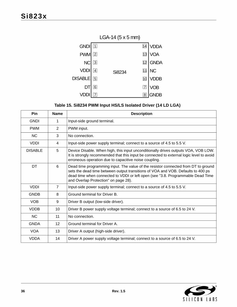
Table 15. Si8234 PWM Input HS/LS Isolated Driver (14 LD LGA)
Pin Name Description
GNDI 1 Input-side ground terminal.
PWM 2 PWM input.
NC 3 No connection.
VDDI 4 Input-side power supply terminal; connect to a source of 4.5 to 5.5 V.
DISABLE 5 Device Disable. When high, this input unconditionally drives outputs VOA, VOB LOW. It is strongly recommended that this input be connected to external logic level to avoid erroneous operation due to capacitive noise coupling.
DT 6 Dead time programming input. The value of the resistor connected from DT to ground sets the dead time between output transitions of VOA and VOB. Defaults to 400 ps dead time when connected to VDDI or left open (see "3.8. Programmable Dead Time and Overlap Protection" on page 28).
VDDI 7 Input-side power supply terminal; connect to a source of 4.5 to 5.5 V.
GNDB 8 Ground terminal for Driver B.
VOB 9 Driver B output (low-side driver).
VDDB 10 Driver B power supply voltage terminal; connect to a source of 6.5 to 24 V.
NC 11 No connection.
GNDA 12 Ground terminal for Driver A.
VOA 13 Driver A output (high-side driver).
VDDA 14 Driver A power supply voltage terminal; connect to a source of 6.5 to 24 V.
LGA-14 (5 x 5 mm)
GNDI
PWM
NC
VDDI
DISABLE
DT
VDDI
VDDA
VOA
GNDA
NC
VDDB
VOB
GNDB
Si8234
1
2
3
4
5
6
7
14
13
12
11
10
7
8

Si823x
Rev. 1.5 37
Table 16. Si8235 Dual Isolated Driver (14 LD LGA)
Pin Name Description
GNDI 1 Input-side ground terminal.
VIA 2 Non-inverting logic input terminal for Driver A.
VIB 3 Non-inverting logic input terminal for Driver B.
VDDI 4 Input-side power supply terminal; connect to a source of 4.5 to 5.5 V.
DISABLE 5 Device Disable. When high, this input unconditionally drives outputs VOA, VOB LOW. It is strongly recommended that this input be connected to external logic level to avoid erroneous operation due to capacitive noise coupling.
NC 6 No connection.
VDDI 7 Input-side power supply terminal; connect to a source of 4.5 to 5.5 V.
GNDB 8 Ground terminal for Driver B.
VOB 9 Driver B output (low-side driver).
VDDB 10 Driver B power supply voltage terminal; connect to a source of 6.5 to 24 V.
NC 11 No connection.
GNDA 12 Ground terminal for Driver A.
VOA 13 Driver A output (high-side driver).
VDDA 14 Driver A power supply voltage terminal; connect to a source of 6.5 to 24 V.
LGA-14 (5 x 5 mm)
GNDI
VIA
VIB
VDDI
DISABLE
NC
VDDI
VDDA
VOA
GNDA
NC
VDDB
VOB
GNDB
Si8235
1
2
3
4
5
6
7
14
13
12
11
10
7
8

Si823x
38 Rev. 1.5
Table 17. Si8236 Dual Isolated Driver (14 LD LGA)
Pin Name Description
GNDI 1 Input-side ground terminal.
VIA 2 Non-inverting logic input terminal for Driver A.
VIB 3 Non-inverting logic input terminal for Driver B.
VDDI 4 Input-side power supply terminal; connect to a source of 4.5 to 5.5 V.
DISABLE 5 Device Disable. When high, this input unconditionally drives outputs VOA, VOB LOW. It is strongly recommended that this input be connected to external logic level to avoid erroneous operation due to capacitive noise coupling.
NC 6 No connection.
VDDI 7 Input-side power supply terminal; connect to a source of 4.5 to 5.5 V.
GNDB 8 Ground terminal for Driver B. GNDA and GNDB pins for the Si8236 are connected together through the thermal pad.
VOB 9 Driver B output (low-side driver).
VDDB 10 Driver B power supply voltage terminal; connect to a source of 6.5 to 24 V.
NC 11 No connection.
GNDA 12 Ground terminal for Driver A.GNDA and GNDB pins for the Si8236 are connected together through the thermal pad.
VOA 13 Driver A output (high-side driver).
VDDA 14 Driver A power supply voltage terminal; connect to a source of 6.5 to 24 V.
LGA-14 (5 x 5 mm)
GNDI
VIA
VIB
VDDI
DISABLE
NC
VDDI
VDDA
VOA
GNDA
NC
VDDB
VOB
GNDB
Si8236
1
2
3
4
5
6
7
14
13
12
11
10
7
8

Si823x
Rev. 1.5 39
6. Ordering Guide
Table 18. Ordering Part Numbers1,2,3
Ordering Part Number (OPN)
Inputs ConfigurationPeak
CurrentUVLO
VoltageIsolation Rating
Temperature Range
Package Type
Legacy Ordering Part Number (OPN)
2.5 kV Only
Wide Body (WB) Package Options
Si8230BB-B-IS VIA, VIBHigh Side/Low Side
0.5 A 8 V
2.5 kVrms –40 to +125 °CSOIC-16
Wide Body
Si8230-A-IS
Si8231BB-B-IS PWMHigh Side/Low Side
Si8231-A-IS
Si8232BB-B-IS VIA,VIB Dual Driver Si8232-A-IS
Si8234CB-C-IS PWMHigh Side/Low Side
4.0 A
10 V N/A
Si8233BB-C-IS VIA,VIBHigh Side/Low Side
8 V
Si8233-B-IS
Si8234BB-C-IS PWMHigh Side/Low Side
Si8234-B-IS
Si8235BB-C-IS VIA,VIB Dual Driver Si8235-B-IS
Si8230AB-B-IS VIA, VIB High Side/Low Side 0.5 A 5 V
2.5 kVrms –40 to +125 °CSOIC-16
Wide Body
N/A
Si8231AB-B-IS PWM N/A
Si8232AB-B-IS VIA,VIB Dual Driver N/A
Si8233AB-C-IS VIA,VIB High Side/Low Side 4.0 A 5 V
N/A
Si8234AB-C-IS PWM N/A
Si8235AB-C-IS VIA,VIB Dual Driver N/A
Notes:1. All packages are RoHS-compliant with peak reflow temperatures of 260 °C according to the JEDEC industry standard
classifications and peak solder temperatures.2. All devices >1 kVRMS are AEC-Q100 qualified.3. “Si” and “SI” are used interchangeably.

Si823x
40 Rev. 1.5
Narrow Body (NB) Package Options
Si8230BB-B-IS1 VIA,VIBHigh Side/Low Side
0.5 A 8 V
2.5 kVrms–40 to +125 °C
SOIC-16Narrow Body
N/A
Si8231BB-B-IS1 PWMHigh Side/Low Side
Si8232BB-B-IS1 VIA,VIB Dual Driver
Si8233BB-C-IS1 VIA,VIBHigh Side/Low Side
4.0 A 8 VSi8234BB-C-IS1 PWMHigh Side/Low Side
Si8235BB-C-IS1 VIA,VIB Dual Driver
Si8235BA-C-IS1 VIA,VIB Dual Driver 1.0 kVrms
Si8230AB-B-IS1 VIA,VIB High Side/Low Side 0.5 A 5 V
2.5 kVrms –40 to +125 °CSOIC-16Narrow Body
N/A
Si8231AB-B-IS1 PWM N/A
Si8232AB-B-IS1 VIA,VIB Dual Driver N/A
Si8233AB-C-IS1 VIA,VIB High Side/Low Side 4.0 A 5 V
N/A
Si8234AB-C-IS1 PWM N/A
Si8235AB-C-IS1 VIA,VIB Dual Driver N/A
Table 18. Ordering Part Numbers1,2,3 (Continued)
Ordering Part Number (OPN)
Inputs ConfigurationPeak
CurrentUVLO
VoltageIsolation Rating
Temperature Range
Package Type
Legacy Ordering Part Number (OPN)
2.5 kV Only
Notes:1. All packages are RoHS-compliant with peak reflow temperatures of 260 °C according to the JEDEC industry standard
classifications and peak solder temperatures.2. All devices >1 kVRMS are AEC-Q100 qualified.3. “Si” and “SI” are used interchangeably.

Si823x
Rev. 1.5 41
LGA Package Options
Si8233CB-C-IM
VIA,VIBHigh Side/Low Side
4.0 A
10 V
2.5 kVrms
–40 to +125 °C
LGA-14 5x5 mm
N/A
Si8233BB-C-IM 8 V Si8233-B-IM
Si8233AB-C-IM 5 V N/A
Si8234BB-C-IM PWM
8 V Si8234-B-IM
Si8234AB-C-IM 5 V N/A
Si8235BB-C-IM
VIA,VIB Dual Driver
8 V Si8235-B-IM
Si8235AB-C-IM 5 V N/A
Si8236BA-C-IM 8 V
1.0 kVrms
LGA-14 5x5 mm
with Thermal
Pad
Si8236-B-IM
Si8236AA-C-IM
5 V
N/A
5 kV Ordering Options
Si8230BD-B-IS VIA, VIBHigh Side/Low Side
0.5 A
8 V 5.0 kVrms –40 to +125 °CSOIC-16
Wide Body
N/A
Si8231BD-B-IS PWMHigh Side/Low Side
Si8232BD-B-IS VIA, VIB Dual Driver
Si8233BD-C-IS VIA, VIBHigh Side/Low Side
4.0 ASi8234BD-C-IS PWM
High Side/Low Side
Si8235BD-C-IS VIA, VIB Dual Driver
Si8230AD-B-IS VIA, VIB High Side/Low Side 0.5 A 5 V
5.0 kVrms –40 to +125 °CSOIC-16
Wide Body
N/A
Si8231AD-B-IS PWM N/A
Si8232AD-B-IS VIA, VIB Dual Driver N/A
Si8233AD-C-IS VIA, VIB High Side/Low Side 4.0 A 5 V
N/A
Si8234AD-C-IS PWM N/A
Si8235AD-C-IS VIA, VIB Dual Driver N/A
Table 18. Ordering Part Numbers1,2,3 (Continued)
Ordering Part Number (OPN)
Inputs ConfigurationPeak
CurrentUVLO
VoltageIsolation Rating
Temperature Range
Package Type
Legacy Ordering Part Number (OPN)
2.5 kV Only
Notes:1. All packages are RoHS-compliant with peak reflow temperatures of 260 °C according to the JEDEC industry standard
classifications and peak solder temperatures.2. All devices >1 kVRMS are AEC-Q100 qualified.3. “Si” and “SI” are used interchangeably.

Si823x
42 Rev. 1.5
3 V VDDI Ordering Options
Si8237AB‐B‐IS1 VIA, VIB Dual Driver0.5 A
5 V
2.5 kVrms
40 to +125 °C
SOIC-16Narrow Body
N/A
Si8237BB‐B‐IS1 VIA, VIB Dual Driver 8 V
Si8238AB‐C‐IS1 VIA, VIB Dual Driver4.0 A
5 V
Si8238BB‐C‐IS1 VIA, VIB Dual Driver 8 V
Si8237AD‐B‐IS VIA, VIB Dual Driver0.5 A
5 V
5.0 kVrmsSOIC-16
Wide Body
Si8237BD‐B‐IS VIA, VIB Dual Driver 8 V
Si8238AD‐C‐IS VIA, VIB Dual Driver4.0 A
5 V
Si8238BD‐C‐IS VIA, VIB Dual Driver 8 V
Table 18. Ordering Part Numbers1,2,3 (Continued)
Ordering Part Number (OPN)
Inputs ConfigurationPeak
CurrentUVLO
VoltageIsolation Rating
Temperature Range
Package Type
Legacy Ordering Part Number (OPN)
2.5 kV Only
Notes:1. All packages are RoHS-compliant with peak reflow temperatures of 260 °C according to the JEDEC industry standard
classifications and peak solder temperatures.2. All devices >1 kVRMS are AEC-Q100 qualified.3. “Si” and “SI” are used interchangeably.
Si823x
Rev. 1.5 43
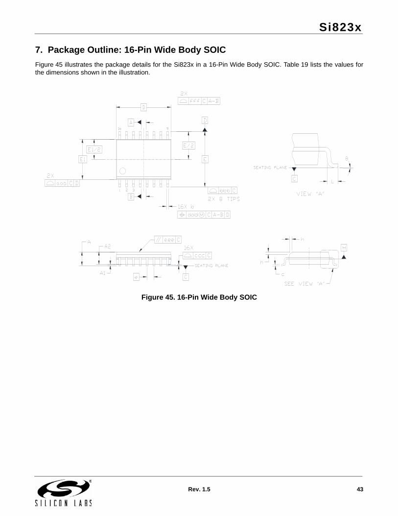
7. Package Outline: 16-Pin Wide Body SOIC
Figure 45 illustrates the package details for the Si823x in a 16-Pin Wide Body SOIC. Table 19 lists the values forthe dimensions shown in the illustration.
Figure 45. 16-Pin Wide Body SOIC
Si823x
44 Rev. 1.5
Table 19. Package Diagram Dimensions
Dimension Min Max
A — 2.65
A1 0.10 0.30
A2 2.05 —
b 0.31 0.51
c 0.20 0.33
D 10.30 BSC
E 10.30 BSC
E1 7.50 BSC
e 1.27 BSC
L 0.40 1.27
h 0.25 0.75
0° 8°
aaa — 0.10
bbb — 0.33
ccc — 0.10
ddd — 0.25
eee — 0.10
fff — 0.20
Notes:1. All dimensions shown are in millimeters (mm) unless otherwise noted.2. Dimensioning and Tolerancing per ANSI Y14.5M-1994.3. This drawing conforms to JEDEC Outline MS-013, Variation AA.4. Recommended reflow profile per JEDEC J-STD-020 specification for
small body, lead-free components.

Si823x
Rev. 1.5 45
8. Land Pattern: 16-Pin Wide Body SOIC
Figure 46 illustrates the recommended land pattern details for the Si823x in a 16-pin wide-body SOIC. Table 20lists the values for the dimensions shown in the illustration.
Figure 46. 16-Pin SOIC Land Pattern
Table 20. 16-Pin Wide Body SOIC Land Pattern Dimensions
Dimension Feature (mm)
C1 Pad Column Spacing 9.40
E Pad Row Pitch 1.27
X1 Pad Width 0.60
Y1 Pad Length 1.90
Notes:1. This Land Pattern Design is based on IPC-7351 pattern SOIC127P1032X265-16AN
for Density Level B (Median Land Protrusion).2. All feature sizes shown are at Maximum Material Condition (MMC) and a card
fabrication tolerance of 0.05 mm is assumed.

Si823x
46 Rev. 1.5
9. Package Outline: 16-Pin Narrow Body SOIC
Figure 47 illustrates the package details for the Si823x in a 16-pin narrow-body SOIC (SO-16). Table 21 lists thevalues for the dimensions shown in the illustration.
Figure 47. 16-pin Small Outline Integrated Circuit (SOIC) Package
Table 21. Package Diagram Dimensions
Dimension Min Max Dimension Min Max
A — 1.75 L 0.40 1.27
A1 0.10 0.25 L2 0.25 BSC
A2 1.25 — h 0.25 0.50
b 0.31 0.51 θ 0° 8°
c 0.17 0.25 aaa 0.10
D 9.90 BSC bbb 0.20
E 6.00 BSC ccc 0.10
E1 3.90 BSC ddd 0.25
e 1.27 BSC
Notes:1. All dimensions shown are in millimeters (mm) unless otherwise noted.2. Dimensioning and Tolerancing per ANSI Y14.5M-1994.3. This drawing conforms to the JEDEC Solid State Outline MS-012, Variation AC.4. Recommended card reflow profile is per the JEDEC/IPC J-STD-020 specification for Small Body
Components.

Si823x
Rev. 1.5 47
10. Land Pattern: 16-Pin Narrow Body SOIC
Figure 48 illustrates the recommended land pattern details for the Si823x in a 16-pin narrow-body SOIC. Table 22lists the values for the dimensions shown in the illustration.
Figure 48. 16-Pin Narrow Body SOIC PCB Land Pattern
Table 22. 16-Pin Narrow Body SOIC Land Pattern Dimensions
Dimension Feature (mm)
C1 Pad Column Spacing 5.40
E Pad Row Pitch 1.27
X1 Pad Width 0.60
Y1 Pad Length 1.55
Notes:1. This Land Pattern Design is based on IPC-7351 pattern SOIC127P600X165-16N
for Density Level B (Median Land Protrusion).2. All feature sizes shown are at Maximum Material Condition (MMC) and a card
fabrication tolerance of 0.05 mm is assumed.

Si823x
48 Rev. 1.5
11. Package Outline: 14 LD LGA (5 x 5 mm)
Figure 49 illustrates the package details for the Si823x in an LGA outline. Table 23 lists the values for thedimensions shown in the illustration.
Figure 49. Si823x LGA Outline
Table 23. Package Diagram Dimensions
Dimension MIN NOM MAX
A 0.74 0.84 0.94
b 0.25 0.30 0.35
D 5.00 BSC
D1 4.15 BSC
e 0.65 BSC
E 5.00 BSC
E1 3.90 BSC
L 0.70 0.75 0.80
L1 0.05 0.10 0.15
aaa — — 0.10
bbb — — 0.10
ccc — — 0.08
ddd — — 0.15
eee — — 0.08
Notes:1. All dimensions shown are in millimeters (mm) unless otherwise noted.2. Dimensioning and Tolerancing per ANSI Y14.5M-1994.

Si823x
Rev. 1.5 49
12. Land Pattern: 14 LD LGA
Figure 50 illustrates the recommended land pattern details for the Si823x in a 14-pin LGA. Table 24 lists the valuesfor the dimensions shown in the illustration.
Figure 50. 14-Pin LGA Land Pattern
Table 24. 14-Pin LGA Land Pattern Dimensions
Dimension (mm)
C1 4.20
E 0.65
X1 0.80
Y1 0.40Notes:General
1. All dimensions shown are in millimeters (mm).2. This Land Pattern Design is based on the IPC-7351 guidelines.3. All dimensions shown are at Maximum Material Condition (MMC). Least
Material Condition (LMC) is calculated based on a Fabrication Allowance of 0.05 mm.
Solder Mask Design4. All metal pads are to be non-solder mask defined (NSMD). Clearance
between the solder mask and the metal pad is to be 60 µm minimum, all the way around the pad.
Stencil Design5. A stainless steel, laser-cut and electro-polished stencil with trapezoidal
walls should be used to assure good solder paste release.6. The stencil thickness should be 0.125 mm (5 mils).7. The ratio of stencil aperture to land pad size should be 1:1.
Card Assembly8. A No-Clean, Type-3 solder paste is recommended.9. The recommended card reflow profile is per the JEDEC/IPC J-STD-020
specification for Small Body Components.

Si823x
50 Rev. 1.5
13. Package Outline: 14 LD LGA with Thermal Pad (5 x 5 mm)
Figure 51 illustrates the package details for the Si8236 ISOdriver in an LGA outline. Table 25 lists the values for thedimensions shown in the illustration.
Figure 51. Si823x LGA Outline with Thermal Pad
Table 25. Package Diagram Dimensions
Dimension MIN NOM MAX
A 0.74 0.84 0.94
b 0.25 0.30 0.35
D 5.00 BSC
D1 4.15 BSC
e 0.65 BSC
E 5.00 BSC
E1 3.90 BSC
L 0.70 0.75 0.80
L1 0.05 0.10 0.15
P1 1.40 1.45 1.50
P2 4.15 4.20 4.25
aaa — — 0.10
bbb — — 0.10
ccc — — 0.08
ddd — — 0.15
eee — — 0.08
Notes:1. All dimensions shown are in millimeters (mm) unless otherwise noted.2. Dimensioning and Tolerancing per ANSI Y14.5M-1994.

Si823x
Rev. 1.5 51
14. Land Pattern: 14 LD LGA with Thermal Pad
Figure 52 illustrates the recommended land pattern details for the Si8236 in a 14-pin LGA with thermal pad.Table 26 lists the values for the dimensions shown in the illustration.
Figure 52. 14-Pin LGA with Thermal Pad Land Pattern
Table 26. 14-Pin LGA with Thermal Pad Land Pattern Dimensions
Dimension (mm)
C1 4.20
C2 1.50
D2 4.25
E 0.65
X1 0.80
Y1 0.40Notes:General:
1. All dimensions shown are in millimeters (mm).2. This Land Pattern Design is based on the IPC-7351 guidelines.3. All dimensions shown are at Maximum Material Condition (MMC). Least
Material Condition (LMC) is calculated based on a Fabrication Allowance of 0.05 mm.
Solder Mask Design:4. All metal pads are to be non-solder mask defined (NSMD). Clearance
between the solder mask and the metal pad is to be 60 µm minimum, all the way around the pad.
Stencil Design:5. A stainless steel, laser-cut and electro-polished stencil with trapezoidal
walls should be used to assure good solder paste release.6. The stencil thickness should be 0.125 mm (5 mils).7. The ratio of stencil aperture to land pad size should be 1:1.
Card Assembly:8. A No-Clean, Type-3 solder paste is recommended.9. The recommended card reflow profile is per the JEDEC/IPC J-STD-020
specification for Small Body Components.

Si823x
52 Rev. 1.5
15. Top Markings
15.1. Si823x Top Marking (16-Pin Wide Body SOIC)
15.2. Top Marking Explanation (16-Pin Wide Body SOIC)
Line 1 Marking:
Base Part Number Ordering Options
See Ordering Guide for more information.
Si823 = ISOdriver product seriesY = Peak output current 0, 1, 2, 7 = 0.5 A
3, 4, 5, 8 = 4.0 A
U = UVLO level A = 5 V; B = 8 V; C = 10 V; D = 12.5 V
V = Isolation rating B = 2.5 kV; C = 3.75 kV; D = 5.0 kV
Line 2 Marking:
YY = YearWW = Workweek
Assigned by the Assembly House. Corresponds to the year and workweek of the mold date.
TTTTTT = Mfg Code Manufacturing Code from Assembly Purchase Order form.
Line 3 Marking:
Circle = 1.5 mm Diameter(Center Justified)
“e4” Pb-Free Symbol
Country of OriginISO Code Abbreviation
TW = Taiwan
Si823YUVYYWWTTTTTT
TW e4

Si823x
Rev. 1.5 53
15.3. Si823x Top Marking (16-Pin Narrow Body SOIC)
15.4. Top Marking Explanation (16-Pin Narrow Body SOIC)
Line 1 Marking:
Base Part Number Ordering Options
See Ordering Guide for more information.
Si823 = ISOdriver product seriesY = Peak output current 0, 1, 2, 7 = 0.5 A
3, 4, 5, 8 = 4.0 A
U = UVLO level A = 5 V; B = 8 V; C = 10 V; D = 12.5 V
V = Isolation rating B = 2.5 kV; C = 3.75 kV; D = 5.0 kV
Line 2 Marking:
YY = YearWW = Workweek
Assigned by the Assembly House. Corresponds to the year and workweek of the mold date.
TTTTTT = Mfg CodeManufacturing Code from Assembly Purchase Order form.
Si823YUVYYWWTTTTTTe4

Si823x
54 Rev. 1.5
15.5. Si823x Top Marking (14 LD LGA)
15.6. Top Marking Explanation (14 LD LGA)
Line 1 Marking: Base Part Number Ordering Options
See Ordering Guide for more information.
Si823 = ISOdriver product seriesY = Peak output current 0, 1, 2 = 0.5 A
3, 4, 5, 6 = 4.0 A
Line 2 Marking: Ordering options U = UVLO level A = 5 V; B = 8 V; C = 10 V; D = 12.5 V
V = Isolation rating A = 1.0 kV; B = 2.5 kV; C = 3.75 kV; D = 5.0 kV
I = –40 to +125 °C ambient temperature rangeM = LGA package type
Line 3 Marking: TTTTTT Manufacturing Code from Assembly
Line 4 Marking: Circle = 1.5 mm diameter Pin 1 identifier
YYWW Manufacturing date code
Si823YUV-IM
TTTTTT YYWW

Si823x
Rev. 1.5 55
DOCUMENT CHANGE LIST
Revision 0.11 to Revision 0.2 Updated all specs to reflect latest silicon revision.
Updated Table 1 on page 6 to include new UVLO options.
Updated Table 8 on page 14 to reflect new maximum package isolation ratings
Added Figures 34, 35, and 36.
Updated Ordering Guide to reflect new package offerings.
Added "3.7.3. Undervoltage Lockout (UVLO)" on page 27 to describe UVLO operation.
Revision 0.2 to Revision 0.3 Moved Sections 2, 3, and 4 to after Section 5.
Updated Tables 14, 15, and 17.Removed Si8230, Si8231, and Si8232 from pinout and
from title.
Updated and added Ordering Guide footnotes.
Updated UVLO specifications in Table 1 on page 6.
Added PWD and Output Supply Active Current specifications in Table 1.
Updated and added typical operating condition graphs in "3.1. Typical Operating Characteristics (0.5 Amp)" on page 17 and "3.2. Typical Operating Characteristics (4.0 Amp)" on page 19.
Revision 0.3 to Revision 1.0 Updated Tables 2, 3, 4, and 5.
Updated “6. Ordering Guide” .Added 5 V UVLO ordering options
Added Device Marking sections.
Revision 1.0 to Revision 1.1 Updated " Features" on page 1.
Updated CMTI specification.
Updated Table 1 on page 6.Updated CMTI specification.
Updated Table 5, “IEC 60747-5-5 Insulation Characteristics*,” on page 13.
Updated "4.2. Dual Driver" on page 31.
Updated "6. Ordering Guide" on page 39.
Replaced pin descriptions on page 1 with chip graphics.
Revision 1.1 to Revision 1.2 Updated "6. Ordering Guide" on page 39.
Updated moisture sensitivity level (MSL) for all package types.
Updated Table 8 on page 14.Added junction temperature spec.
Updated Table 2 on page 11 with new notes.
Added Table 17 and pinout.
Updated Figures 19, 20, 21, and 22 to reflect correct y-axis scaling.
Updated Figure 44 on page 31.
Updated "4.3. Dual Driver with Thermally Enhanced Package (Si8236)" on page 31.
Updated "7. Package Outline: 16-Pin Wide Body SOIC" on page 43.
Updated Table 19, “Package Diagram Dimensions,” on page 44.
Change references to 1.5 kVRMS rated devices to 1.0 kVRMS throughout.
Updated "3.5. Power Dissipation Considerations" on page 23.
Revision 1.2 to Revision 1.3 Added Si8237/8 throughout.
Updated Table 1 on page 6.
Updated Figure 4 on page 9.
UpdatedFigure 5 on page 9.
Added Figure 6 on page 10.
Updated Table 10 on page 21.Created Notes 1 and 2.
Updated "3.8. Programmable Dead Time and Overlap Protection" on page 28.Removed references to Figures 26A and 26B.
Updated Table 18 on page 39.Added Si8235-BA-C-IS1 ordering part number.Added table note.
Revision 1.3 to Revision 1.4 Updated "6. Ordering Guide" on page 39.
Updated “ 3 V VDDI Ordering Options” .
Revision 1.4 to Revision 1.5 Updated Table 1, input and output supply current.
Added references to AEC-Q100 qualified throughout.
Changed all 60747-5-2 references to 60747-5-5.
Added references to CQC throughout.
Updated pin descriptions throughout.Corrected dead time default to 400 ps from 1 ns.
Updated Table 18, Ordering Part Numbers.Removed moisture sensitivity level table notes.
Si823x
56 Rev. 1.5
CONTACT INFORMATIONSilicon Laboratories Inc.
400 West Cesar ChavezAustin, TX 78701Tel: 1+(512) 416-8500Fax: 1+(512) 416-9669Toll Free: 1+(877) 444-3032
Please visit the Silicon Labs Technical Support web page:https://www.silabs.com/support/pages/contacttechnicalsupport.aspxand register to submit a technical support request.
Patent NoticeSilicon Labs invests in research and development to help our customers differentiate in the market with innovative low-power, small size, analog-intensive mixed-signal solutions. Silicon Labs' extensive patent portfolio is a testament to our unique approach and world-class engineering team.
Silicon Laboratories and Silicon Labs are trademarks of Silicon Laboratories Inc.Other products or brandnames mentioned herein are trademarks or registered trademarks of their respective holders.
The information in this document is believed to be accurate in all respects at the time of publication but is subject to change without notice. Silicon Laboratories assumes no responsibility for errors and omissions, and disclaims responsibility for any consequences resulting from the use of information included herein. Additionally, Silicon Laboratories assumes no responsibility for the functioning of undescribed fea-tures or parameters. Silicon Laboratories reserves the right to make changes without further notice. Silicon Laboratories makes no warran-ty, representation or guarantee regarding the suitability of its products for any particular purpose, nor does Silicon Laboratories assume any liability arising out of the application or use of any product or circuit, and specifically disclaims any and all liability, including without limitation consequential or incidental damages. Silicon Laboratories products are not designed, intended, or authorized for use in applications intend-ed to support or sustain life, or for any other application in which the failure of the Silicon Laboratories product could create a situation where personal injury or death may occur. Should Buyer purchase or use Silicon Laboratories products for any such unintended or unauthorized application, Buyer shall indemnify and hold Silicon Laboratories harmless against all claims and damages.