Embed Size (px)
Citation preview

VDD
SCLA0
GND
OutputBuffer
Power DownControl Logic
ResistorNetwork
Ref (+) REF(-)12-BitDAC
I2CControlLogic
DACRegister
Power-OnReset
VOUT
SDA
D A C 7 512
DAC7571
www.ti.com SLAS374D –FEBRUARY 2003–REVISED JANUARY 2014
+2.7 V to +5.5 V, I2C INTERFACE (RECEIVE ONLY), VOLTAGE OUTPUT,12-BIT DIGITAL-TO-ANALOG CONVERTER
Check for Samples: DAC7571
1FEATURESDESCRIPTION
2• Micropower Operation: 140 µA @ 5 VThe DAC7571 is a low-power, single channel, 12-bit• Power-On Reset to Zero buffered voltage output DAC. Its on-chip precision
• +2.7-V to +5.5-V Power Supply output amplifier allows rail-to-rail output swing to beachieved. The DAC7571 utilizes an I2C compatible• Specified Monotonic by Designtwo wire serial interface that operates at clock rates• Settling Time: 10 µs to ±0.003%FS up to 3.4 Mbps with address support of up to two
• I2C™ Interface up to 3.4 Mbps DAC7571s on the same data bus.• On-Chip Output Buffer Amplifier, Rail-to-Rail The output voltage range of the DAC is set to VDD.Operation The DAC7571 incorporates a power-on-reset circuit• Double-Buffered Input Register that ensures that the DAC output powers up at zero
volts and remains there until a valid write to the• Address Support for up to Two DAC7571sdevice takes place. The DAC7571 contains a power-• Small 6-Lead SOT Package down feature, accessed via the internal control
• Operation From –40°C to 105°C register, that reduces the current consumption of thedevice to 50 nA at 5 V.
APPLICATIONS The low power consumption of this part in normal• Process Control operation makes it ideally suited for portable battery
operated equipment. The power consumption is less• Data Acquisition Systemsthan 0.7 mW at VDD = 5 V reducing to 1 µW in power-• Closed-Loop Servo Control down mode.
• PC PeripheralsThe DAC7571 is available in a 6-lead SOT 23• Portable Instrumentation package.
1
Please be aware that an important notice concerning availability, standard warranty, and use in critical applications ofTexas Instruments semiconductor products and disclaimers thereto appears at the end of this data sheet.
2I2C is a trademark of Philips Corporation.PRODUCTION DATA information is current as of publication date. Copyright © 2003–2014, Texas Instruments IncorporatedProducts conform to specifications per the terms of the TexasInstruments standard warranty. Production processing does notnecessarily include testing of all parameters.

A0SCLSDA
6
5
4
1
2
3
VOUT
GNDVDD
D771
1
2
3
6
5
4
YM
LL
(TOP VIEW)
(BOTTOM VIEW)
Lot Trace Code
DAC7571
SLAS374D –FEBRUARY 2003–REVISED JANUARY 2014 www.ti.com
These devices have limited built-in ESD protection. The leads should be shorted together or the device placed in conductive foam duringstorage or handling to prevent electrostatic damage to the MOS gates.
This integrated circuit can be damaged by ESD. Texas Instruments recommends that all integrated circuits be handled withappropriate precautions. Failure to observe proper handling and installation procedures can cause damage.
ESD damage can range from subtle performance degradation to complete device failure. Precision integrated circuits may be moresusceptible to damage because very small parametric changes could cause the device not to meet its published specifications.
PACKAGE/ORDERING INFORMATIONPACKAGE SPECIFIED PACKAGE ORDERINGPRODUCT PACKAGE DESIGNATO TEMPERATURE TRANSPORT MEDIAMARKING NUMBERR RANGE
DAC7571IDBVT 250-Piece Small Tape and ReelDAC7571 SOT23-6 DBV –40°C to +105°C D771
DAC7571IDBVR 3000-Piece Tape and Reel
PIN CONFIGURATIONS
PIN DESCRIPTION (SOT23-6)PIN NAME DESCRIPTION1 VOUT Analog output voltage from DAC
Ground reference point for all2 GND circuitry on the part3 VDD Analog Voltage Supply Input4 SDA Serial Data Input5 SCL Serial Clock Input6 A0 Device Address Select
LOT Year (3 = 2003); Month (1–9 = JAN–SEP; A=OCT,TRACE B=NOV, C=DEC); LL – Random code generatedCODE: when assembly is requested
ABSOLUTE MAXIMUM RATINGS (1)
UNITSVDD to GND –0.3 V to +6 VDigital Input voltage to GND –0.3 V to +VDD +0.3 VVOUT to GND –0.3 V to +VDD +0.3 VOperating temperature range –40°C to +105°CStorage temperature range –65°C to +150°CJunction temperature range (TJ max) +150°CPower dissipation (TJmax - TA)R ΘJA
Thermal impedance, R ΘJA 240°C/WLead temperature, soldering Vapor phase (60 s) 215°C
Infrared (15 s) 220°C
(1) Stresses above those listed under “Absolute Maximum Ratings” may cause permanent damage to the device. Exposure to absolutemaximum conditions for extended periods may affect device reliability.
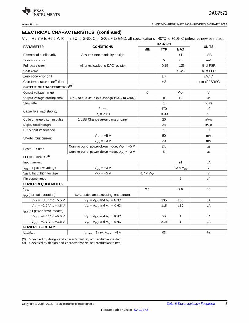
ELECTRICAL CHARACTERISTICSVDD = +2.7 V to +5.5 V; RL = 2 kΩ to GND; CL = 200 pF to GND; all specifications –40°C to +105°C unless otherwise noted.
DAC7571PARAMETER CONDITIONS UNITS
MIN TYP MAXSTATIC PERFORMANCE (1)
Resolution 12 BitsRelative accuracy ±0.195 % of FSR
(1) Linearity calculated using a reduced code range of 48 to 4047; output unloaded.
2 Submit Documentation Feedback Copyright © 2003–2014, Texas Instruments Incorporated
Product Folder Links: DAC7571
DAC7571
www.ti.com SLAS374D –FEBRUARY 2003–REVISED JANUARY 2014
ELECTRICAL CHARACTERISTICS (continued)VDD = +2.7 V to +5.5 V; RL = 2 kΩ to GND; CL = 200 pF to GND; all specifications –40°C to +105°C unless otherwise noted.
DAC7571PARAMETER CONDITIONS UNITS
MIN TYP MAXDifferential nonlinearity Assured monotonic by design ±1 LSBZero code error 5 20 mVFull-scale error All ones loaded to DAC register –0.15 –1.25 % of FSRGain error ±1.25 % of FSRZero code error drift ± 7 µV/°CGain temperature coefficient ± 3 ppm of FSR/°COUTPUT CHARACTERISTICS (2)
Output voltage range 0 VDD VOutput voltage settling time 1/4 Scale to 3/4 scale change (400H to C00H) 8 10 µsSlew rate 1 V/µs
RL =∞ 470 pFCapacitive load stability
RL = 2 kΩ 1000 pFCode change glitch impulse 1 LSB Change around major carry 20 nV-sDigital feedthrough 0.5 nV-sDC output impedance 1 Ω
VDD = +5 V 50 mAShort-circuit current
VDD = +3 V 20 mAComing out of power-down mode, VDD = +5 V 2.5 µs
Power-up timeComing out of power-down mode, VDD = +3 V 5 µs
LOGIC INPUTS (3)
Input current ±1 µAVINL, Input low voltage VDD = +3 V 0.3 × VDD VVINH, Input high voltage VDD = +5 V 0.7 × VDD VPin capacitance 3 pFPOWER REQUIREMENTSVDD 2.7 5.5 VIDD (normal operation) DAC active and excluding load current
VDD = +3.6 V to +5.5 V VIH = VDD and VIL = GND 135 200 µAVDD = +2.7 V to +3.6 V VIH = VDD and VIL = GND 115 160 µA
IDD (all power-down modes)VDD = +3.6 V to +5.5 V VIH = VDD and VIL = GND 0.2 1 µAVDD = +2.7 V to +3.6 V VIH = VDD and VIL = GND 0.05 1 µA
POWER EFFICIENCYIOUT/IDD ILOAD = 2 mA, VDD = +5 V 93 %
(2) Specified by design and characterization, not production tested.(3) Specified by design and characterization, not production tested.
Copyright © 2003–2014, Texas Instruments Incorporated Submit Documentation Feedback 3
Product Folder Links: DAC7571
DAC7571
SLAS374D –FEBRUARY 2003–REVISED JANUARY 2014 www.ti.com
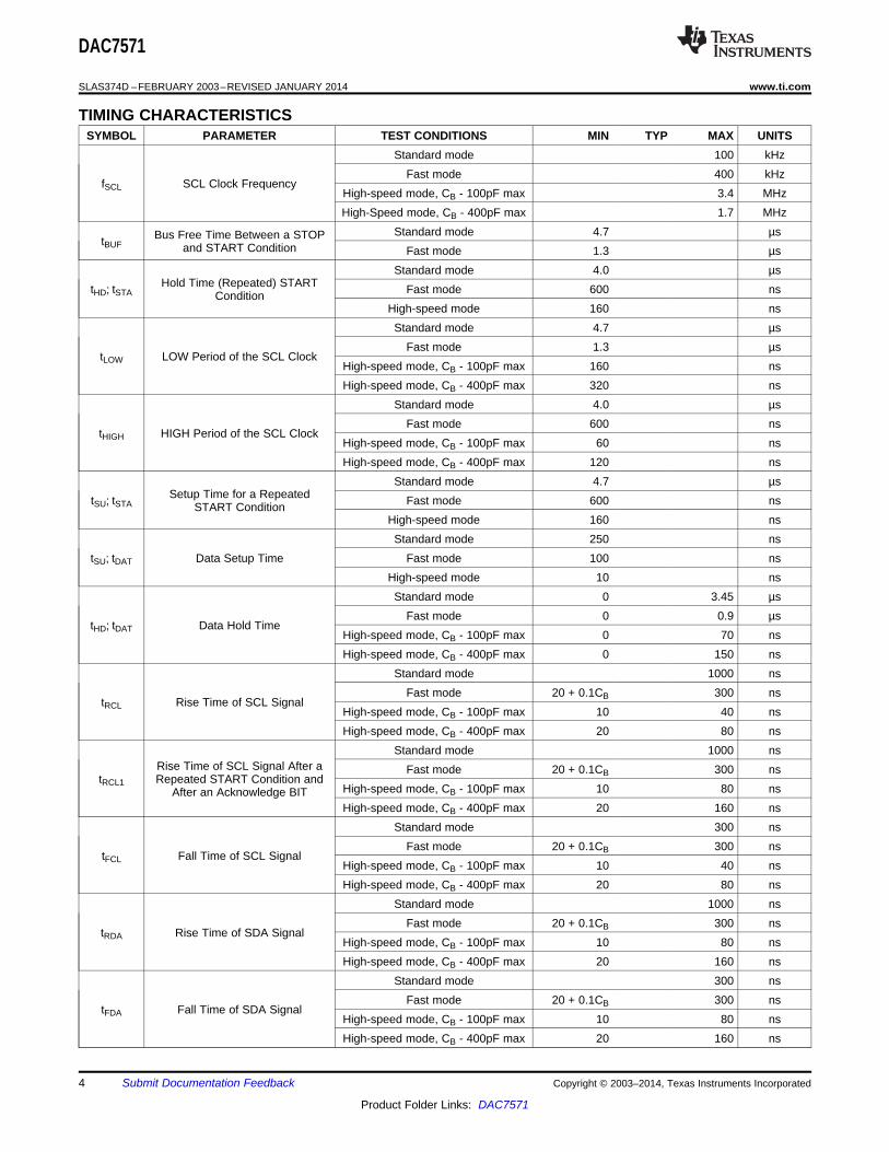
TIMING CHARACTERISTICSSYMBOL PARAMETER TEST CONDITIONS MIN TYP MAX UNITS
Standard mode 100 kHzFast mode 400 kHz
fSCL SCL Clock FrequencyHigh-speed mode, CB - 100pF max 3.4 MHzHigh-Speed mode, CB - 400pF max 1.7 MHz
Standard mode 4.7 µsBus Free Time Between a STOPtBUF and START Condition Fast mode 1.3 µsStandard mode 4.0 µs
Hold Time (Repeated) STARTtHD; tSTA Fast mode 600 nsConditionHigh-speed mode 160 nsStandard mode 4.7 µs
Fast mode 1.3 µstLOW LOW Period of the SCL Clock
High-speed mode, CB - 100pF max 160 nsHigh-speed mode, CB - 400pF max 320 ns
Standard mode 4.0 µsFast mode 600 ns
tHIGH HIGH Period of the SCL ClockHigh-speed mode, CB - 100pF max 60 nsHigh-speed mode, CB - 400pF max 120 ns
Standard mode 4.7 µsSetup Time for a RepeatedtSU; tSTA Fast mode 600 nsSTART Condition
High-speed mode 160 nsStandard mode 250 ns
tSU; tDAT Data Setup Time Fast mode 100 nsHigh-speed mode 10 nsStandard mode 0 3.45 µs
Fast mode 0 0.9 µstHD; tDAT Data Hold Time
High-speed mode, CB - 100pF max 0 70 nsHigh-speed mode, CB - 400pF max 0 150 ns
Standard mode 1000 nsFast mode 20 + 0.1CB 300 ns
tRCL Rise Time of SCL SignalHigh-speed mode, CB - 100pF max 10 40 nsHigh-speed mode, CB - 400pF max 20 80 ns
Standard mode 1000 nsRise Time of SCL Signal After a Fast mode 20 + 0.1CB 300 ns
tRCL1 Repeated START Condition andHigh-speed mode, CB - 100pF max 10 80 nsAfter an Acknowledge BITHigh-speed mode, CB - 400pF max 20 160 ns
Standard mode 300 nsFast mode 20 + 0.1CB 300 ns
tFCL Fall Time of SCL SignalHigh-speed mode, CB - 100pF max 10 40 nsHigh-speed mode, CB - 400pF max 20 80 ns
Standard mode 1000 nsFast mode 20 + 0.1CB 300 ns
tRDA Rise Time of SDA SignalHigh-speed mode, CB - 100pF max 10 80 nsHigh-speed mode, CB - 400pF max 20 160 ns
Standard mode 300 nsFast mode 20 + 0.1CB 300 ns
tFDA Fall Time of SDA SignalHigh-speed mode, CB - 100pF max 10 80 nsHigh-speed mode, CB - 400pF max 20 160 ns
4 Submit Documentation Feedback Copyright © 2003–2014, Texas Instruments Incorporated
Product Folder Links: DAC7571
DAC7571
www.ti.com SLAS374D –FEBRUARY 2003–REVISED JANUARY 2014
TIMING CHARACTERISTICS (continued)SYMBOL PARAMETER TEST CONDITIONS MIN TYP MAX UNITS
Standard mode 4.0 µstSU; tSTO Setup Time for STOP Condition Fast mode 600 ns
High-speed mode 160 nsCB Capacitive Load for SDA and SCL 400 pF
Fast mode 50 nstSP Pulse Width of Spike Suppressed
High-speed mode 10 nsStandard modeNoise Margin at the HIGH Level
VNH for Each Connected Device Fast mode 0.2VDD V(Including Hysteresis) High-speed mode
Standard modeNoise Margin at the LOW Level forVNL Each Connected Device Fast mode 0.1VDD V
(Including Hysteresis) High-speed mode
Copyright © 2003–2014, Texas Instruments Incorporated Submit Documentation Feedback 5
Product Folder Links: DAC7571

−30
−20
−10
0
10
20
30
−50 −30 −10 10 30 50 70 90 110
Zer
o-S
cale
Err
or −
mV
T − Temperature − C
−30
−20
−10
0
10
20
30
−50 −30 −10 10 30 50 70 90 110
Zer
o-S
cale
Err
or −
mV
T − Temperature − C
−8−6−4−2
02468
LE −
LS
BD
LE −
LS
B
−1
−0.5
0
0.5
1
0 512 1024 1536 2048 2560 3072 3584 4096Digital Input Code
Digital Input Code
Out
put E
rror
−m
V
−16
−8
0
8
16
0 512 1024 1536 2048 2560 3072 3584 4096
−8−6−4−2
02468
LE −
LS
B
−1
−0.5
0
0.5
1
0 512 1024 1536 2048 2560 3072 3584 4096
Digital Input Code
DLE
− L
SB
−8−6−4−2
02468
−1
−0.5
0
0.5
1
0 512 1024 1536 2048 2560 3072 3584 4096Digital Input Code
LE −
LS
BD
LE −
LS
B
DAC7571
SLAS374D –FEBRUARY 2003–REVISED JANUARY 2014 www.ti.com
TYPICAL CHARACTERISTICS: VDD = +5 VAt TA = +25°C, +VDD = +5 V, unless otherwise noted.
LINEARITY ERROR AND LINEARITY ERROR ANDDIFFERENTIAL LINEARITY ERROR DIFFERENTIAL LINEARITY ERROR
vs vsCODE (-40°C) CODE (+25 ° C )
Figure 1. Figure 2.
LINEARITY ERROR ANDDIFFERENTIAL LINEARITY ERROR
vsCODE (+105° C) TYPICAL TOTAL UNADJUSTED ERROR
Figure 3. Figure 4.
ZERO-SCALE ERROR FULL-SCALE ERRORvs vs
TEMPERATURE TEMPERATURE
Figure 5. Figure 6.
6 Submit Documentation Feedback Copyright © 2003–2014, Texas Instruments Incorporated
Product Folder Links: DAC7571
2.7
I DD (
nA)
VDD (V)
3.2 3.7 4.2 4.7 5.2 5.7
100
90
80
70
60
50
40
30
20
10
0
+25°C
–40°C
+105°C
0
50
100
150
200
250
300
2.7 3.2 3.7 4.2 4.7 5.2 5.7
− S
uppl
y C
urre
nt −
I DD
Aµ
VDD − Supply V oltage − V
0
50
100
150
200
250
300
−50 −30 −10 10 30 50 70 90 110
− S
uppl
y C
urre
nt −
I DD
Aµ
T − Temperature − C
0
100
200
300
400
500
CODE000H 200H 600H A00H E00H FFFH
I DD
µ A−
Sup
ply
Cur
rent
−
0
VO
UT (
V)
ISOURCE/SINK (mA)
5 10 15
5
4
3
2
1
0
DAC Loaded with FFFH
DAC Loaded with 000H0
500
1000
1500
2000
250080 90 10
0
110
120
130
140
150
160
170
180
190
200
IDD − Supply Current − A
f − F
requ
ency
− H
z
DAC7571
www.ti.com SLAS374D –FEBRUARY 2003–REVISED JANUARY 2014
TYPICAL CHARACTERISTICS: VDD = +5 V (continued)At TA = +25°C, +VDD = +5 V, unless otherwise noted.
IDD HISTOGRAM SOURCE AND SINK CURRENT CAPABILITY
Figure 7. Figure 8.
SUPPLY CURRENT SUPPLY CURRENTvs vs
CODE TEMPERATURE
Figure 9. Figure 10.
SUPPLY CURRENT POWER-DOWN CURRENTvs vs
SUPPLY VOLTAGE SUPPLY VOLTAGE
Figure 11. Figure 12.
Copyright © 2003–2014, Texas Instruments Incorporated Submit Documentation Feedback 7
Product Folder Links: DAC7571

Time (1µs/div)
CLK (5V/div)
VOUT (1V/div)
Half-Scale Code ChangeC00H to 400H
Output Loaded with2kΩ and 200pF to GND
Time (20µs/div)
Loaded with 2kΩ to VDD.
VDD (1V/div)
VOUT (1V/div)
Time (1µs/div)
CLK (5V/div)
VOUT (1V/div)
Full-Scale Code ChangeFFFH to 000H
Output Loaded with2kΩ and 200pF to GND
HALF-SCALE SETTLING TIME
Time (1µs/div)
CLK (5V/div)
VOUT (1V/div)
Half-Scale Code Change400H to C00H
Output Loaded with2kΩ and 200pF to GND
0
I DD (
µA)
VLOGIC (V)
1 2 3 4 5
2500
2000
1500
1000
500
0
CLK (5V/div)
VOUT (1V/div)
Time (1µs/div)
Full-Scale Code Change000H to FFFH
Output Loaded with2kΩ and 200pF to GND
DAC7571
SLAS374D –FEBRUARY 2003–REVISED JANUARY 2014 www.ti.com
TYPICAL CHARACTERISTICS: VDD = +5 V (continued)At TA = +25°C, +VDD = +5 V, unless otherwise noted.
SUPPLY CURRENTvs
LOGIC INPUT VOLTAGE FULL-SCALE SETTLING TIME
Figure 13. Figure 14.
FULL-SCALE SETTLING TIME HALF-SCALE SETTLING TIME
Figure 15. Figure 16.
HALF-SCALE SETTLING TIME POWER-ON RESET TO 0V
Figure 17. Figure 18.
8 Submit Documentation Feedback Copyright © 2003–2014, Texas Instruments Incorporated
Product Folder Links: DAC7571
Time (0.5µs/div)
Loaded with 2kΩand 200pF to GND.Code Change:800H to 7FFH.
VO
UT
(20m
V/d
iv)
Time (5µs/div)
CLK (5V/div)
VOUT (1V/div)
DAC7571
www.ti.com SLAS374D –FEBRUARY 2003–REVISED JANUARY 2014
TYPICAL CHARACTERISTICS: VDD = +5 V (continued)At TA = +25°C, +VDD = +5 V, unless otherwise noted.
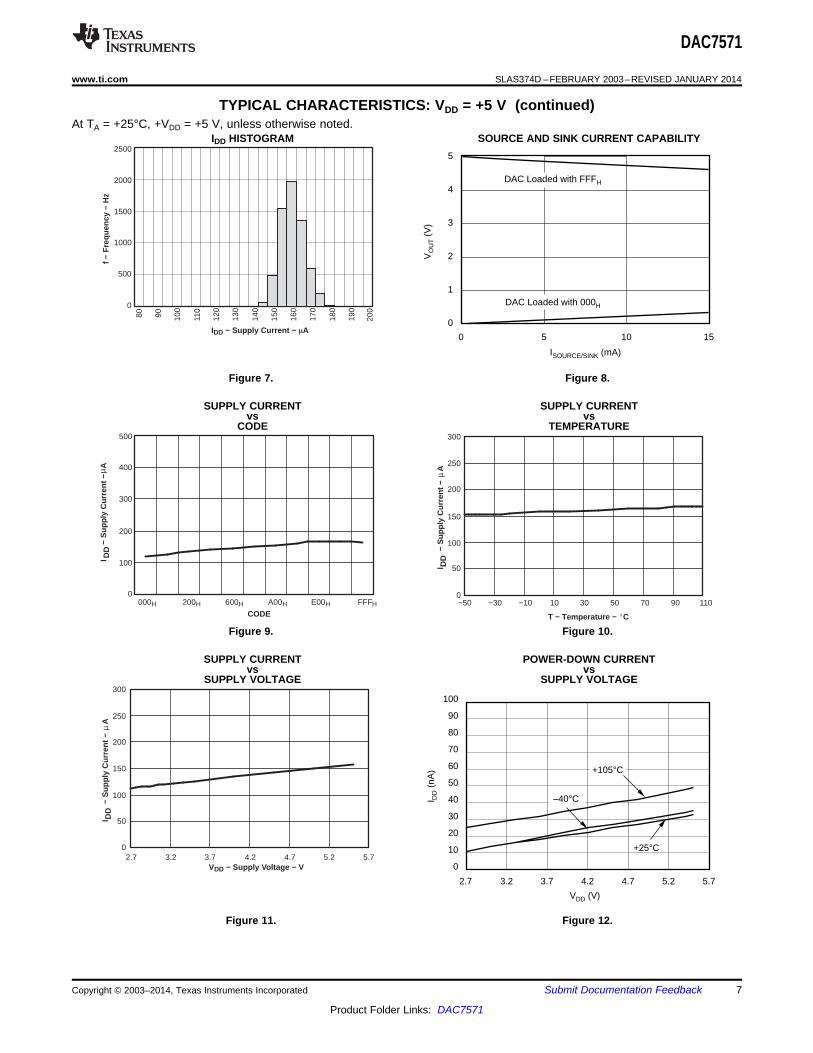
EXITING POWER-DOWN(800HLoaded) CODE CHANGE GLITCH
Figure 19. Figure 20.
Copyright © 2003–2014, Texas Instruments Incorporated Submit Documentation Feedback 9
Product Folder Links: DAC7571

−30
−20
−10
0
10
20
30
−50 −30 −10 10 30 50 70 90 110
Zer
o-S
cale
Err
or −
mV
T − Temperature − C
−30
−20
−10
0
10
20
30
−50 −30 −10 10 30 50 70 90 110
T − Temperature − C
Ful
l-Sca
le E
rror
− m
V
−16
−8
0
8
16
0 512 1024 1536 2048 2560 3072 3584
Digital Input Code
4096
Out
put E
rror
− m
V
−8−6−4−2
02468
−1
−0.5
0
0.5
1
0 512 1024 1536 2048 2560 3072 3584 4096
Digital Input Code
LE −
LS
BD
LE −
LS
B
−8−6−4−2
02468
−1
−0.5
0
0.5
1
0 512 1024 1536 2048 2560 3072 3584 4096
Digital Input Code
LE −
LS
BD
LE −
LS
B
−8−6−4−2
02468
−1
−0.5
0
0.5
1
0 512 1024 1536 2048 2560 3072 3584 4096
Digital Input Code
LE −
LS
BD
LE −
LS
B
DAC7571
SLAS374D –FEBRUARY 2003–REVISED JANUARY 2014 www.ti.com
TYPICAL CHARACTERISTICS: VDD = +2.7 VAt TA = +25°C, +VDD = +2.7V, unless otherwise noted.
LINEARITY ERROR AND LINEARITY ERROR ANDDIFFERENTIAL LINEARITY ERROR DIFFERENTIAL LINEARITY ERROR
vs vsCODE (-40 °C) CODE (+25 °C)
Figure 21. Figure 22.
LINEARITY ERROR ANDDIFFERENTIAL LINEARITY ERROR
vsCODE (+105 °C) ABSOLUTE ERROR
Figure 23. Figure 24.
ZERO-SCALE ERROR FULL-SCALE ERRORvs vs
TEMPERATURE TEMPERATURE
Figure 25. Figure 26.
10 Submit Documentation Feedback Copyright © 2003–2014, Texas Instruments Incorporated
Product Folder Links: DAC7571
0
I DD (
µA)
VLOGIC (V)
1 2 3 4 5
2500
2000
1500
1000
500
0
FULL-SCALE SETTLING TIME
Time (1µs/div)
CLK (2.7V/div)
VOUT (1V/div)
Full-Scale Code Change000H to FFFH
Output Loaded with2kΩ and 200pF to GND
0
100
200
300
400
500
000H 02FH 200H 400H 600H 800H A00
H
C00H E00H FCFH FFFH
IDD − Supply Current − A
f − F
requ
ency
− H
z
0
50
100
150
200
250
300
−50 −30 −10 10 30 50 70 90 110
− S
uppl
y C
urre
nt −
I DD
Aµ
T − Temperature − C
SOURCE AND SINK CURRENT CAPABILITY
0
VO
UT (
V)
ISOURCE/SINK (mA)
5 10 15
3
2
1
0
DAC Loaded with FFFH
DAC Loaded with 000H
VDD = +3V
0
500
1000
1500
2000
250080 90 10
0
110
120
130
140
150
160
170
180
190
200
IDD − Supply Current − A
f − F
requ
ency
− H
z
DAC7571
www.ti.com SLAS374D –FEBRUARY 2003–REVISED JANUARY 2014
TYPICAL CHARACTERISTICS: VDD = +2.7 V (continued)At TA = +25°C, +VDD = +2.7V, unless otherwise noted.
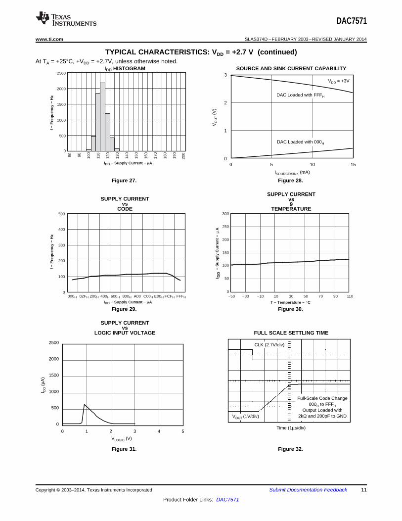
IDD HISTOGRAM SOURCE AND SINK CURRENT CAPABILITY
Figure 27. Figure 28.
SUPPLY CURRENTSUPPLY CURRENT vs
vs 9CODE TEMPERATURE
Figure 29. Figure 30.
SUPPLY CURRENTvs
LOGIC INPUT VOLTAGE FULL SCALE SETTLING TIME
Figure 31. Figure 32.
Copyright © 2003–2014, Texas Instruments Incorporated Submit Documentation Feedback 11
Product Folder Links: DAC7571

Time (0.5µs/div)
Loaded with 2kΩand 200pF to GND.Code Change:800H to 7FFH.
VO
UT
(20m
V/d
iv)
Time (5µs/div)
CLK (2.7V/div)
VOUT (1V/div)
Time (1µs/div)
CLK (2.7V/div)
VOUT (1V/div)
Half-Scale Code ChangeC00H to 400H
Output Loaded with2kΩ and 200pF to GND
POWER-ON RESET to 0V
Time (20µs/div)
Time (1µs/div)
CLK (2.7V/div)
VOUT (1V/div) Full-Scale Code ChangeFFFH to 000H
Output Loaded with2kΩ and 200pF to GND
Time (1µs/div)
CLK (2.7V/div)
VOUT (1V/div)
Half-Scale Code Change400H to C00H
Output Loaded with2kΩ and 200pF to GND
DAC7571
SLAS374D –FEBRUARY 2003–REVISED JANUARY 2014 www.ti.com
TYPICAL CHARACTERISTICS: VDD = +2.7 V (continued)At TA = +25°C, +VDD = +2.7V, unless otherwise noted.
FULL SCALE SETTLING TIME HALF SCALE SETTLING TIME
Figure 33. Figure 34.
HALF SCALE SETTLING TIME POWER ON RESET 0 V
Figure 35. Figure 36.
EXITING-POWER DOWN (800HLoaded) CODE CHANGE GLITCH
Figure 37. Figure 38.
12 Submit Documentation Feedback Copyright © 2003–2014, Texas Instruments Incorporated
Product Folder Links: DAC7571
R
R
R
R
VDD
GND
To OutputAmplifier
VOUT VDDD
4096
REF (+)
REF (-)
ResistorString
OutputAmplifier
VOUT
GND
VDD
DAC Register
DAC7571
www.ti.com SLAS374D –FEBRUARY 2003–REVISED JANUARY 2014
THEORY OF OPERATION
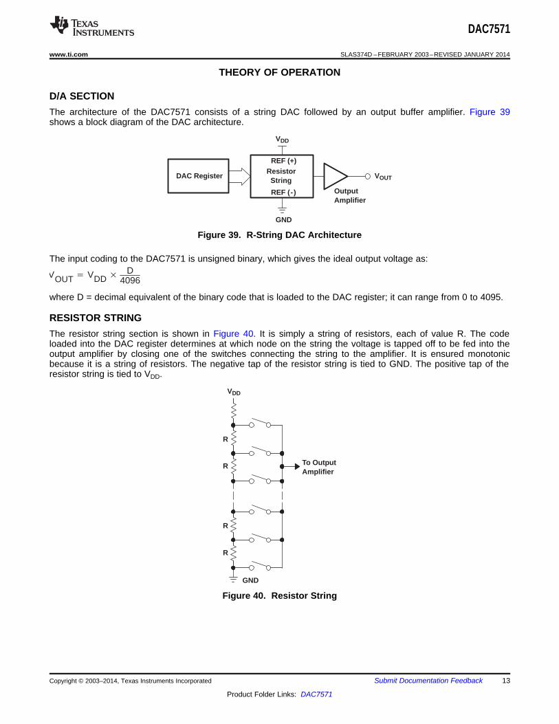
D/A SECTIONThe architecture of the DAC7571 consists of a string DAC followed by an output buffer amplifier. Figure 39shows a block diagram of the DAC architecture.
Figure 39. R-String DAC Architecture
The input coding to the DAC7571 is unsigned binary, which gives the ideal output voltage as:
where D = decimal equivalent of the binary code that is loaded to the DAC register; it can range from 0 to 4095.
RESISTOR STRINGThe resistor string section is shown in Figure 40. It is simply a string of resistors, each of value R. The codeloaded into the DAC register determines at which node on the string the voltage is tapped off to be fed into theoutput amplifier by closing one of the switches connecting the string to the amplifier. It is ensured monotonicbecause it is a string of resistors. The negative tap of the resistor string is tied to GND. The positive tap of theresistor string is tied to VDD.
Figure 40. Resistor String
Copyright © 2003–2014, Texas Instruments Incorporated Submit Documentation Feedback 13
Product Folder Links: DAC7571

Not Acknowledge
Acknowledge
1 2 8 9
Clock Pulse forAcknowledgement
S
STARTCondition
Data Outputby Transmitter
Data Outputby Receiver
SCL FromMaster
StartCondition
SDA
StopCondition
SDA
SCL
S P
SCL
DAC7571
SLAS374D –FEBRUARY 2003–REVISED JANUARY 2014 www.ti.com
OUTPUT AMPLIFIERThe output buffer amplifier is capable of generating rail-to-rail voltages on its output which gives an output rangeof 0 V to VDD. It is capable of driving a load of 2kΩ in parallel with 1000 pF to GND. The source and sinkcapabilities of the output amplifier can be seen in the typical characteristics. The slew rate is 1V/µs with a half-scale settling time of 8 µs with the output unloaded.
I2C InterfaceThe DAC7571 uses an I2C interface as defined by Philips Semiconductor to receive data in slave mode (see I2C-Bus Specification, Version 2.1, January 2000). The DAC7571 supports the following data transfer modes,described in the I2C-Bus Specification: Standard Mode (100 kbit/s), Fast Mode (400 kbit/s) and High-SpeedMode (3.4 Mbit/s). Ten-bit addressing and general call addressing are not supported.
For simplicity, standard mode and fast mode are referred to as F/S-mode and high-speed mode is referred to asHS-mode.
The 2-wire I2C serial bus protocol operates as follows:• The Master initiates data transfer by establishing a Start condition. The Start condition is defined when a high-
to-low transition occurs on the SDA line while SCL is high, as shown in Figure 41. The byte following the startcondition is the address byte consisting of the 7-bit slave address followed by the W bit.
Figure 41. START and STOP Conditions
• The addressed Slave responds by pulling the SDA pin low during the ninth clock pulse, termed theAcknowledge bit (see Figure 42). At this stage all other devices on the bus remain idle while the selecteddevice waits for data to be written to its shift register.
Figure 42. Acknowledge on the I2C Bus
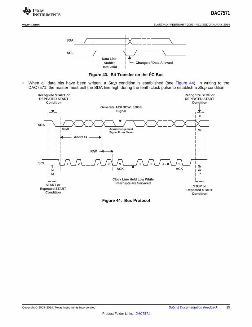
• Data is transmitted over the serial bus in sequences of nine clock cycles (8 data bits followed by anacknowledge bit. The transitions on the SDA line must occur during the low period of SCL and remain stableduring the high period of SCL (see Figure 43).
14 Submit Documentation Feedback Copyright © 2003–2014, Texas Instruments Incorporated
Product Folder Links: DAC7571
Recognize START orREPEATED START
Condition
Recognize STOP orREPEATED START
ConditionGenerate ACKNOWLEDGE
Signal
AcknowledgementSignal From Slave
SDA
SCL
MSB
P
Sr
SrorP
SorSr
START orRepeated START
Condition
STOP orRepeated START
Condition
Clock Line Held Low WhileInterrupts are Serviced
1 2 7 8 9ACK
1 2 3 - 8 9ACK
Address
R/W
Change of Data AllowedData Line
Stable;Data Valid
SDA
SCL
DAC7571
www.ti.com SLAS374D –FEBRUARY 2003–REVISED JANUARY 2014
Figure 43. Bit Transfer on the I2C Bus
• When all data bits have been written, a Stop condition is established (see Figure 44). In writing to theDAC7571, the master must pull the SDA line high during the tenth clock pulse to establish a Stop condition.
Figure 44. Bus Protocol
Copyright © 2003–2014, Texas Instruments Incorporated Submit Documentation Feedback 15
Product Folder Links: DAC7571
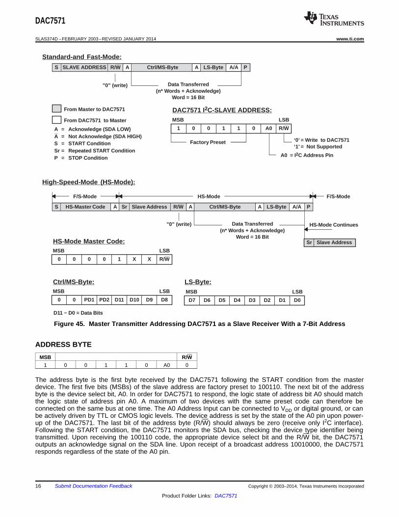
SLAVE ADDRESS R/W A Ctrl/MS-Byte A LS-Byte A/A P
”0” (write) Data Transferred(n* Words + Acknowledge)
Word = 16 Bit
From Master to DAC7571
From DAC7571 to Master
A = Acknowledge (SDA LOW)A = Not Acknowledge (SDA HIGH)S = START ConditionSr = Repeated START ConditionP = STOP Condition
DAC7571 I2C-SLAVE ADDRESS:
1 0 0 1 1 0 A0 R/W
MSB LSB
Factory Preset
A0 = I2C Address Pin
Standard-and Fast-Mode:
S
HS-Master Code R/W A Ctrl/MS-Byte A LS-Byte A/A P
”0” (write) Data Transferred(n* Words + Acknowledge)
Word = 16 Bit
High-Speed-Mode (HS-Mode):
S A Sr Slave Address
HS-Mode Continues
F/S-Mode HS-Mode F/S-Mode
Sr Slave Address
0 0 0 0 1 X X R/W
MSB LSB
HS-Mode Master Code:
0 0 PD1 PD2 D11 D10 D9 D8
MSB LSB
Ctrl/MS-Byte:
D7 D6 D5 D4 D3 D2 D1 D0
MSB LSB
LS-Byte:
D11 − D0 = Data Bits
‘0’ = Write to DAC7571‘1’ = Not Supported
DAC7571
SLAS374D –FEBRUARY 2003–REVISED JANUARY 2014 www.ti.com
Figure 45. Master Transmitter Addressing DAC7571 as a Slave Receiver With a 7-Bit Address
ADDRESS BYTEMSB R/W
1 0 0 1 1 0 A0 0
The address byte is the first byte received by the DAC7571 following the START condition from the masterdevice. The first five bits (MSBs) of the slave address are factory preset to 100110. The next bit of the addressbyte is the device select bit, A0. In order for DAC7571 to respond, the logic state of address bit A0 should matchthe logic state of address pin A0. A maximum of two devices with the same preset code can therefore beconnected on the same bus at one time. The A0 Address Input can be connected to VDD or digital ground, or canbe actively driven by TTL or CMOS logic levels. The device address is set by the state of the A0 pin upon power-up of the DAC7571. The last bit of the address byte (R/W) should always be zero (receive only I2C interface).Following the START condition, the DAC7571 monitors the SDA bus, checking the device type identifier beingtransmitted. Upon receiving the 100110 code, the appropriate device select bit and the R/W bit, the DAC7571outputs an acknowledge signal on the SDA line. Upon receipt of a broadcast address 10010000, the DAC7571responds regardless of the state of the A0 pin.
16 Submit Documentation Feedback Copyright © 2003–2014, Texas Instruments Incorporated
Product Folder Links: DAC7571
DAC7571
www.ti.com SLAS374D –FEBRUARY 2003–REVISED JANUARY 2014
MASTER TRANSMITTER WRITING TO A SLAVE RECEIVER (DAC7571) IN STANDARD/FASTMODESI2C protocol starts when the bus is idle, that is, when SDA and SCL lines are stable high. The master then pullsthe SDA line low while SCL is still high indicting that serial data transfer has started. This is called a startcondition, and can only be asserted by the master. After the start condition, the master generates the serial clockand puts out an address byte. While generating the bit stream, the master ensures the timing for valid data. Foreach valid I2C bit, the SDA line should remain stable during the entire high period of the SCL line. The addressbyte consists of 7 address bits (1001 100, assuming A0=0) and a direction bit (R/W=0). After sending theaddress byte, the master generates a ninth SCL pulse and monitors the state of the SDA line during the highperiod of this ninth clock cycle.
The SDA line being pulled low by a receiver during the high period of this 9th clock cycle is called anacknowledge signal. If the master receives an acknowledge signal, it knows that a DAC7571 successfullymatched the address which the master sent. Upon the receipt of this acknowledge, the master knows that thecommunication link with a DAC7571 has been established and more data can be sent. The master continues bysending a Control/MS-byte, which sets DAC7571 operation mode and specifies the first 4 MSBs of data. Aftersending the Control/MS-byte, the master expects an acknowledge signal from the DAC7571. Upon the receipt ofthe acknowledge, the master sends an LS-byte that represents the 8 least significant bits of DAC7571's 12-bitconversion data. After receiving the LS-byte, the DAC7571 sends an acknowledge. At the falling edge of theacknowledge signal, following the LS-byte, the DAC7571 performs a digital to analog conversion. For furtherDAC updates, the master can keep repeating Control/MS-byte and LS-byte sequences expecting anacknowledge after each byte. After the required number of digital to analog conversions is complete, the mastercan break the communication link with the DAC7571 by pulling the SDA line from low to high while SCL line ishigh. This is called a stop condition. A stop condition brings the bus back to idle (SDA and SCL both high). Astop condition indicates that communication with the DAC7571 has ended. All devices on the bus, including theDAC7571, waits for a new start condition followed by a matching address byte. DAC7571 stays in a programmedstate until the receipt of a stop condition.
Table 1. Write Sequence in Standard/Fast ModesTransmitter MSB 6 5 4 3 2 1 LSB CommentMaster Start Begin Sequence (1)
Write Addressing (LSB=0, R/W =Master 1 0 0 1 1 0 A0 0 0)DAC7571 DAC7571 AcknowledgesMaster 0 0 PD1 PD0 D11 D10 D9 D8 Writing Control/MS-ByteDAC7571 DAC7571 AcknowledgesMaster D7 D6 D5 D4 D3 D2 D1 D0 Writing LS-ByteDAC7571 DAC7571 AcknowledgesMaster Stop or Repeated Start (2) Done
(1) Once DAC7571 is addressed, high-byte-low-byte sequences can repeat until a stop condition is received.(2) Use repeated start to secure bus operation and loop back to the stage of write addressing for next Write.
POWER-ON RESETThe DAC7571 contains a power-on reset circuit that controls the output voltage during power-up. On power-up,the DAC register is filled with zeros and the output voltage is 0 V. It remains at a zero-code output until a validwrite sequence is made to the DAC. This is useful in applications where it is important to know the state of theDAC output while it is in the process of powering up.
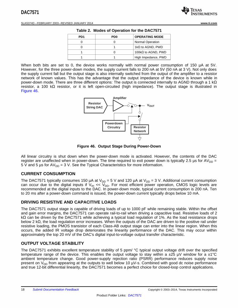
POWER-DOWN MODESThe DAC7571 contains four separate modes of operation. These modes are programmable via two bits (PD1and PD0). Table 2 shows how the state of these bits correspond to the mode of operation.
Copyright © 2003–2014, Texas Instruments Incorporated Submit Documentation Feedback 17
Product Folder Links: DAC7571
ResistorString DAC
PowerdownCircuitry
VOUT
Amplifier
ResistorNetwork
DAC7571
SLAS374D –FEBRUARY 2003–REVISED JANUARY 2014 www.ti.com
Table 2. Modes of Operation for the DAC7571PD1 PD0 OPERATING MODE
0 0 Normal Operation0 1 1kΩ to AGND, PWD1 0 100kΩ to AGND, PWD1 1 High Impedance, PWD
When both bits are set to 0, the device works normally with normal power consumption of 150 µA at 5V.However, for the three power-down modes, the supply current falls to 200 nA at 5V (50 nA at 3 V). Not only doesthe supply current fall but the output stage is also internally switched from the output of the amplifier to a resistornetwork of known values. This has the advantage that the output impedance of the device is known while inpower-down mode. There are three different options: The output is connected internally to AGND through a 1 kΩresistor, a 100 kΩ resistor, or it is left open-circuited (high impedance). The output stage is illustrated inFigure 46.
Figure 46. Output Stage During Power-Down
All linear circuitry is shut down when the power-down mode is activated. However, the contents of the DACregister are unaffected when in power-down. The time required to exit power down is typically 2.5 µs for AVDD =5 V and 5 µs for AVDD = 3 V. See the Typical Characteristics for more information.
CURRENT CONSUMPTIONThe DAC7571 typically consumes 150 µA at VDD = 5 V and 120 µA at VDD = 3 V. Additional current consumptioncan occur due to the digital inputs if VIH << VDD. For most efficient power operation, CMOS logic levels arerecommended at the digital inputs to the DAC. In power-down mode, typical current consumption is 200 nA. Tento 20 ms after a power-down command is issued, the power-down current typically drops below 10 mA.
DRIVING RESISTIVE AND CAPACITIVE LOADSThe DAC7571 output stage is capable of driving loads of up to 1000 pF while remaining stable. Within the offsetand gain error margins, the DAC7571 can operate rail-to-rail when driving a capacitive load. Resistive loads of 2kΩ can be driven by the DAC7571 while achieving a typical load regulation of 1%. As the load resistance dropsbelow 2 kΩ, the load regulation error increases. When the outputs of the DAC are driven to the positive rail underresistive loading, the PMOS transistor of each Class-AB output stage can enter into the linear region. When thisoccurs, the added IR voltage drop deteriorates the linearity performance of the DAC. This may occur withinapproximately the top 20 mV of the DAC's digital input-to-voltage output transfer characteristic.
OUTPUT VOLTAGE STABILITYThe DAC7571 exhibits excellent temperature stability of 5 ppm/ °C typical output voltage drift over the specifiedtemperature range of the device. This enables the output voltage to stay within a ±25 µV window for a ±1°Cambient temperature change. Good power-supply rejection ratio (PSRR) performance reduces supply noisepresent on VDD from appearing at the outputs to well below 10 µV-s. Combined with good dc noise performanceand true 12-bit differential linearity, the DAC7571 becomes a perfect choice for closed-loop control applications.
18 Submit Documentation Feedback Copyright © 2003–2014, Texas Instruments Incorporated
Product Folder Links: DAC7571

REF02
15 V
5 V
1.14 mA
A0SCL
SDA
I2CInterface
VOUT = 0 V to 5 VDAC7571
DAC7571
www.ti.com SLAS374D –FEBRUARY 2003–REVISED JANUARY 2014
APPLICATIONS
USING REF02 AS A POWER SUPPLY FOR THE DAC7571Due to the extremely low supply current required by the DAC7571, a possible configuration is to use a REF02+5V precision voltage reference to supply the required voltage to the DAC7571's supply input as well as thereference input, as shown in Figure 47. This is especially useful if the power supply is quite noisy or if the systemsupply voltages are at some value other than 5 V. The REF02 will output a steady supply voltage for theDAC7571. If the REF02 is used, the current it needs to supply to the DAC7571 is 150 µA typical and 200 µA maxfor VDD = 5 V. When a DAC output is loaded, the REF02 also needs to supply the current to the load. The totaltypical current required (with a 5 mW load on a given DAC output) is: 135 µA + (5 mW/5 V) = 1.14 mA.
The load regulation of the REF02 is typically (0.005%×VDD)/mA, which results in an error of 285 mV for the 1.14mA current drawn from it. This corresponds to a 0.2 LSB error for a 0 V to 5 V output range.
Figure 47. REF02 as Power Supply to DAC7571
LAYOUT
A precision analog component requires careful layout, adequate bypassing, and clean, well-regulated powersupplies.
The power applied to VDD should be well regulated and low noise. Switching power supplies and DC/DCconverters will often have high-frequency glitches or spikes riding on the output voltage. In addition, digitalcomponents can create similar high-frequency spikes as their internal logic switches states. This noise can easilycouple into the DAC output voltage through various paths between the power connections and analog output.
As with the GND connection, VDD should be connected to a +5 V power supply plane or trace that is separatefrom the connection for digital logic until they are connected at the power entry point. In addition, the 1 µF to 10µF and 0.1 µF bypass capacitors are strongly recommended. In some situations, additional bypassing may berequired, such as a 100µF electrolytic capacitor or even a Pi filter made up of inductors and capacitors—alldesigned to essentially low-pass filter the +5 V supply, removing the high-frequency noise.
Copyright © 2003–2014, Texas Instruments Incorporated Submit Documentation Feedback 19
Product Folder Links: DAC7571

DAC7571
SLAS374D –FEBRUARY 2003–REVISED JANUARY 2014 www.ti.com
REVISION HISTORYNOTE: Page numbers of current version may differ from previous versions.
Changes from Revision C (May 2006) to Revision D Page
• Corrected several typographical errors in the Theory of Operation section. ...................................................................... 14
20 Submit Documentation Feedback Copyright © 2003–2014, Texas Instruments Incorporated
Product Folder Links: DAC7571
PACKAGE OPTION ADDENDUM
www.ti.com 10-Dec-2020
Addendum-Page 1
PACKAGING INFORMATION
Orderable Device Status(1)
Package Type PackageDrawing
Pins PackageQty
Eco Plan(2)
Lead finish/Ball material
(6)
MSL Peak Temp(3)
Op Temp (°C) Device Marking(4/5)
Samples
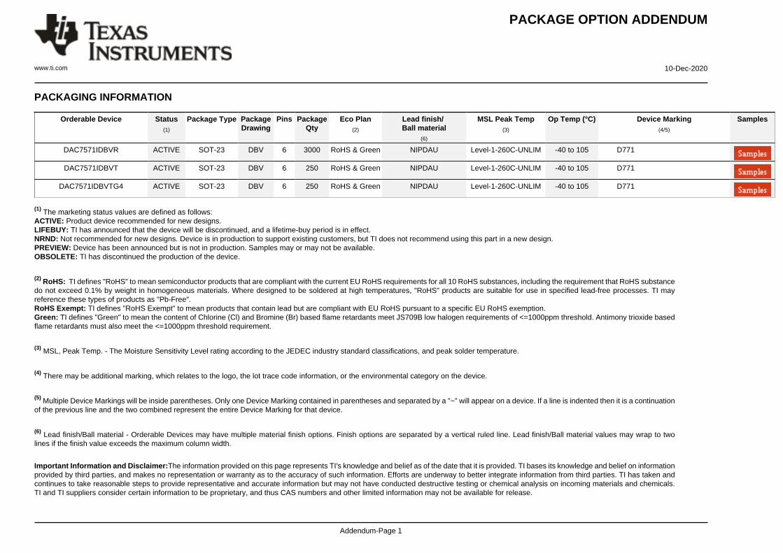
DAC7571IDBVR ACTIVE SOT-23 DBV 6 3000 RoHS & Green NIPDAU Level-1-260C-UNLIM -40 to 105 D771
DAC7571IDBVT ACTIVE SOT-23 DBV 6 250 RoHS & Green NIPDAU Level-1-260C-UNLIM -40 to 105 D771
DAC7571IDBVTG4 ACTIVE SOT-23 DBV 6 250 RoHS & Green NIPDAU Level-1-260C-UNLIM -40 to 105 D771
(1) The marketing status values are defined as follows:ACTIVE: Product device recommended for new designs.LIFEBUY: TI has announced that the device will be discontinued, and a lifetime-buy period is in effect.NRND: Not recommended for new designs. Device is in production to support existing customers, but TI does not recommend using this part in a new design.PREVIEW: Device has been announced but is not in production. Samples may or may not be available.OBSOLETE: TI has discontinued the production of the device.
(2) RoHS: TI defines "RoHS" to mean semiconductor products that are compliant with the current EU RoHS requirements for all 10 RoHS substances, including the requirement that RoHS substancedo not exceed 0.1% by weight in homogeneous materials. Where designed to be soldered at high temperatures, "RoHS" products are suitable for use in specified lead-free processes. TI mayreference these types of products as "Pb-Free".RoHS Exempt: TI defines "RoHS Exempt" to mean products that contain lead but are compliant with EU RoHS pursuant to a specific EU RoHS exemption.Green: TI defines "Green" to mean the content of Chlorine (Cl) and Bromine (Br) based flame retardants meet JS709B low halogen requirements of <=1000ppm threshold. Antimony trioxide basedflame retardants must also meet the <=1000ppm threshold requirement.
(3) MSL, Peak Temp. - The Moisture Sensitivity Level rating according to the JEDEC industry standard classifications, and peak solder temperature.
(4) There may be additional marking, which relates to the logo, the lot trace code information, or the environmental category on the device.
(5) Multiple Device Markings will be inside parentheses. Only one Device Marking contained in parentheses and separated by a "~" will appear on a device. If a line is indented then it is a continuationof the previous line and the two combined represent the entire Device Marking for that device.
(6) Lead finish/Ball material - Orderable Devices may have multiple material finish options. Finish options are separated by a vertical ruled line. Lead finish/Ball material values may wrap to twolines if the finish value exceeds the maximum column width.
Important Information and Disclaimer:The information provided on this page represents TI's knowledge and belief as of the date that it is provided. TI bases its knowledge and belief on informationprovided by third parties, and makes no representation or warranty as to the accuracy of such information. Efforts are underway to better integrate information from third parties. TI has taken andcontinues to take reasonable steps to provide representative and accurate information but may not have conducted destructive testing or chemical analysis on incoming materials and chemicals.TI and TI suppliers consider certain information to be proprietary, and thus CAS numbers and other limited information may not be available for release.
PACKAGE OPTION ADDENDUM
www.ti.com 10-Dec-2020
Addendum-Page 2
In no event shall TI's liability arising out of such information exceed the total purchase price of the TI part(s) at issue in this document sold by TI to Customer on an annual basis.

TAPE AND REEL INFORMATION
*All dimensions are nominal
Device PackageType
PackageDrawing
Pins SPQ ReelDiameter
(mm)
ReelWidth
W1 (mm)
A0(mm)
B0(mm)
K0(mm)
P1(mm)
W(mm)
Pin1Quadrant
DAC7571IDBVR SOT-23 DBV 6 3000 178.0 9.0 3.23 3.17 1.37 4.0 8.0 Q3
DAC7571IDBVT SOT-23 DBV 6 250 178.0 9.0 3.23 3.17 1.37 4.0 8.0 Q3
PACKAGE MATERIALS INFORMATION
www.ti.com 24-Apr-2020
Pack Materials-Page 1

*All dimensions are nominal
Device Package Type Package Drawing Pins SPQ Length (mm) Width (mm) Height (mm)
DAC7571IDBVR SOT-23 DBV 6 3000 180.0 180.0 18.0
DAC7571IDBVT SOT-23 DBV 6 250 180.0 180.0 18.0
PACKAGE MATERIALS INFORMATION
www.ti.com 24-Apr-2020
Pack Materials-Page 2
www.ti.com
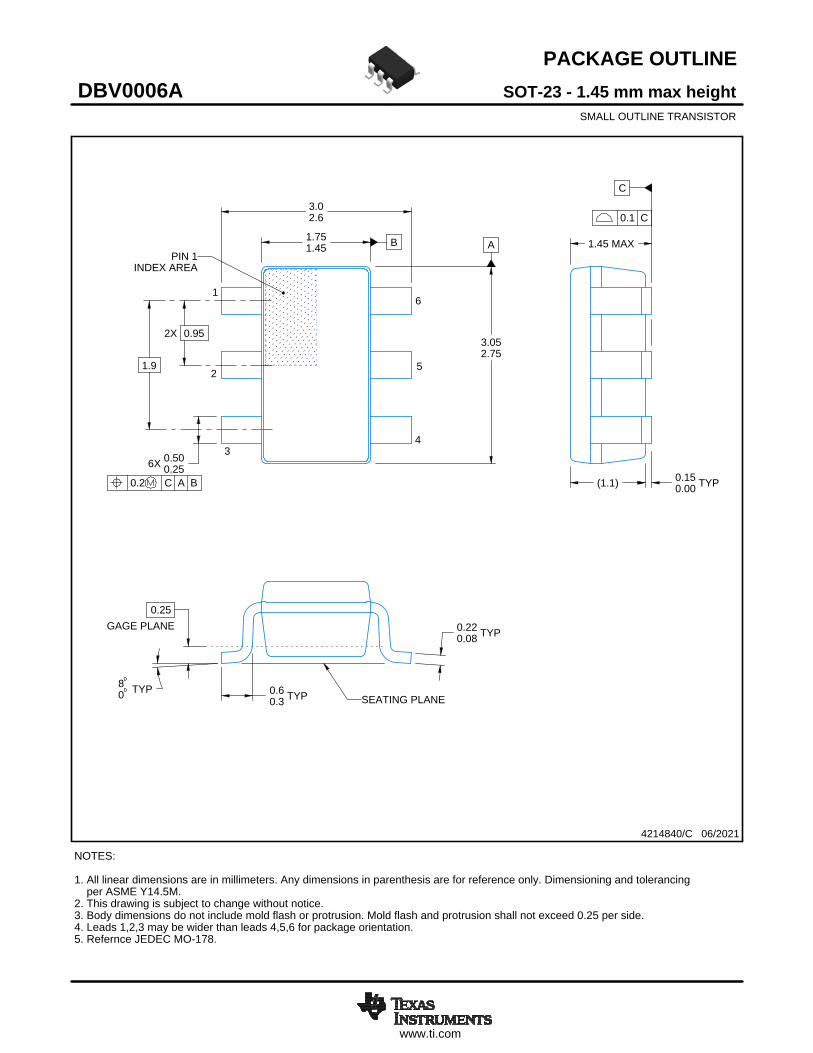
PACKAGE OUTLINE
C
0.220.08 TYP
0.25
3.02.6
2X 0.95
1.45 MAX
0.150.00 TYP
6X 0.500.25
0.60.3 TYP
80 TYP
1.9
A
3.052.75
B1.751.45
(1.1)
SOT-23 - 1.45 mm max heightDBV0006ASMALL OUTLINE TRANSISTOR
4214840/C 06/2021
NOTES: 1. All linear dimensions are in millimeters. Any dimensions in parenthesis are for reference only. Dimensioning and tolerancing per ASME Y14.5M.2. This drawing is subject to change without notice.3. Body dimensions do not include mold flash or protrusion. Mold flash and protrusion shall not exceed 0.25 per side.4. Leads 1,2,3 may be wider than leads 4,5,6 for package orientation.5. Refernce JEDEC MO-178.
0.2 C A B
1
34
52
INDEX AREAPIN 1
6
GAGE PLANE
SEATING PLANE
0.1 C
SCALE 4.000

www.ti.com
EXAMPLE BOARD LAYOUT
0.07 MAXARROUND
0.07 MINARROUND
6X (1.1)
6X (0.6)
(2.6)
2X (0.95)
(R0.05) TYP
4214840/C 06/2021
SOT-23 - 1.45 mm max heightDBV0006ASMALL OUTLINE TRANSISTOR
NOTES: (continued) 6. Publication IPC-7351 may have alternate designs. 7. Solder mask tolerances between and around signal pads can vary based on board fabrication site.
SYMM
LAND PATTERN EXAMPLEEXPOSED METAL SHOWN
SCALE:15X
PKG
1
3 4
52
6
SOLDER MASKOPENINGMETAL UNDER
SOLDER MASK
SOLDER MASKDEFINED
EXPOSED METAL
METALSOLDER MASKOPENING
NON SOLDER MASKDEFINED
(PREFERRED)
SOLDER MASK DETAILS
EXPOSED METAL
www.ti.com
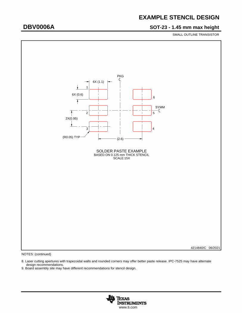
EXAMPLE STENCIL DESIGN
(2.6)
2X(0.95)
6X (1.1)
6X (0.6)
(R0.05) TYP
SOT-23 - 1.45 mm max heightDBV0006ASMALL OUTLINE TRANSISTOR
4214840/C 06/2021
NOTES: (continued) 8. Laser cutting apertures with trapezoidal walls and rounded corners may offer better paste release. IPC-7525 may have alternate design recommendations. 9. Board assembly site may have different recommendations for stencil design.
SOLDER PASTE EXAMPLEBASED ON 0.125 mm THICK STENCIL
SCALE:15X
SYMM
PKG
1
3 4
52
6

IMPORTANT NOTICE AND DISCLAIMERTI PROVIDES TECHNICAL AND RELIABILITY DATA (INCLUDING DATASHEETS), DESIGN RESOURCES (INCLUDING REFERENCEDESIGNS), APPLICATION OR OTHER DESIGN ADVICE, WEB TOOLS, SAFETY INFORMATION, AND OTHER RESOURCES “AS IS”AND WITH ALL FAULTS, AND DISCLAIMS ALL WARRANTIES, EXPRESS AND IMPLIED, INCLUDING WITHOUT LIMITATION ANYIMPLIED WARRANTIES OF MERCHANTABILITY, FITNESS FOR A PARTICULAR PURPOSE OR NON-INFRINGEMENT OF THIRDPARTY INTELLECTUAL PROPERTY RIGHTS.These resources are intended for skilled developers designing with TI products. You are solely responsible for (1) selecting the appropriateTI products for your application, (2) designing, validating and testing your application, and (3) ensuring your application meets applicablestandards, and any other safety, security, or other requirements. These resources are subject to change without notice. TI grants youpermission to use these resources only for development of an application that uses the TI products described in the resource. Otherreproduction and display of these resources is prohibited. No license is granted to any other TI intellectual property right or to any third partyintellectual property right. TI disclaims responsibility for, and you will fully indemnify TI and its representatives against, any claims, damages,costs, losses, and liabilities arising out of your use of these resources.TI’s products are provided subject to TI’s Terms of Sale (https:www.ti.com/legal/termsofsale.html) or other applicable terms available eitheron ti.com or provided in conjunction with such TI products. TI’s provision of these resources does not expand or otherwise alter TI’sapplicable warranties or warranty disclaimers for TI products.IMPORTANT NOTICE
Mailing Address: Texas Instruments, Post Office Box 655303, Dallas, Texas 75265Copyright © 2021, Texas Instruments Incorporated


![GH Everyware 2.7 Update & Notes · t ä w ä r r v v v v o ] v](https://img.pdfslide.us/doc/110x75/5f7310c1cf25fc45f361c86b/gh-everyware-27-update-notes-t-w-r-r-v-v-v-v-o-v.jpg)