Embed Size (px)
Citation preview

TLV1571, TLV15782.7 V TO 5.5 V, 1-/8-CHANNEL, 10-BIT,
PARALLEL ANALOG-TO-DIGITAL CONVERTERS
SLAS170D –MARCH 1999 – REVISED JULY 2000
1POST OFFICE BOX 655303 • DALLAS, TEXAS 75265
features
Fast Throughput Rate: 1.25 MSPS at 5 V, 625 KSPS at 3 V
Wide Analog Input: 0 V to AV DD Differential Nonlinearity Error: < ± 1 LSB
Integral Nonlinearity Error: < ± 1 LSB
8-to-1 Analog MUX – TLV1578
Internal OSC
Single 2.7-V to 5.5-V Supply Operation
Low Power: 12 mW at 3 V and 35 mW at 5 V
Auto Power Down of 1 mA Max
Software Power Down: 10 µA Max
Hardware Configurable
DSP and Microcontroller CompatibleParallel Interface
Binary/Twos Complement Output
Hardware Controlled Extended Sampling
Channel Sweep Mode Operation andChannel Select
Hardware or Software Start of Conversion
applications
Mass Storage and HDD
Automotive
Digital Servos
Process Control
General-Purpose DSP
Image Sensor Processing
descriptionThe TLV1571/1578 is a 10-bit data acquisition system that combines an 8-channel input multiplexer (MUX), ahigh-speed 10-bit ADC, and a parallel interface. The device contains two on-chip control registers allowingcontrol of channel selection, software conversion start, and power down via the bidirectional parallel port. Thecontrol registers can be set to a default mode by applying a dummy RD signal when WR is tied low. This allowsthe TLV1571/1578 to be configured by hardware. The MUX is independently accessible. This allows the user toinsert a signal conditioning circuit such as an antialiasing filter or an amplifier, if required, between the MUX andthe ADC. Therefore, one signal conditioning circuit can be used for all eight channels. The TLV1571 is a singlechannel analog input device with all the same functions as the TLV1578.
The TLV1571/TLV1578 operates from a single 2.7-V to 5.5-V power supply. It accepts an analog input rangefrom 0 V to AVDD and digitizes the input at a maximum 1.25 MSPS throughput rate at 5 V. The power dissipationsare only 12 mW with a 3-V supply or 35 mW with a 5-V supply. The device features an auto power-down modethat automatically powers down to 1 mA 50 ns after conversion is performed. In software power-down mode, theADC is further powered down to only 10 µA.
Copyright 2000, Texas Instruments IncorporatedPRODUCTION DATA information is current as of publication date.Products conform to specifications per the terms of Texas Instrumentsstandard warranty. Production processing does not necessarily includetesting of all parameters.
Please be aware that an important notice concerning availability, standard warranty, and use in critical applications ofTexas Instruments semiconductor products and disclaimers thereto appears at the end of this data sheet.
12345678910111213141516
32313029282726252423222120191817
CH0CH1CH2CH3
CSWRRD
CLKDGNDDVDD
INT/EOCD0D1D2D3D4
CH7CH6CH5CH4MOAINAVDDAGNDREFMREFPCSTARTD9/A1D8/A0D7D6D5
TLV1578DA PACKAGE
(TOP VIEW)
NC – No internal connection
1234 56789101112
242322212019181716151413
CSWRRD
CLKDGNDDVDD
INT/EOCD0D1D2D3D4
NCAINAVDDAGNDREFMREFPCSTARTD9/A1D8/A0D7D6D5
TLV1571DW OR PW PACKAGE
(TOP VIEW)

TLV1571, TLV15782.7 V TO 5.5 V, 1-/8-CHANNEL, 10-BIT,PARALLEL ANALOG-TO-DIGITAL CONVERTERS
SLAS170D –MARCH 1999 – REVISED JULY 2000
2 POST OFFICE BOX 655303 • DALLAS, TEXAS 75265
description (continued)
Very high throughput rate, simple parallel interface, and low power consumption make the TLV1571/TLV1578an ideal choice for high-speed digital signal processing requiring multiple analog inputs.
AVAILABLE OPTIONS
PACKAGE
TA 32 TSSOP(DA)
24 SOP(DW)
24 TSSOP(PW)
0°C to 70°C TLV1578CDA TLV1571CDW TLV1571CPW
–40°C to 85°C TLV1578IDA TLV1571IDW TLV1571IPW
functional block diagram – TLV1571/78
InternalClock
CLK
CSRD INT/EOC
MUX
10-BITSAR ADC
Input Registersand Control Logic
WR
CSTART
REFP
ThreeStateLatch
AVDD
D0 – D7
D8/A0D9/A1
REFM DVDD
DGNDAGND
MUXCH0 – CH7
MO AIN
TLV1578 Only

TLV1571, TLV15782.7 V TO 5.5 V, 1-/8-CHANNEL, 10-BIT,
PARALLEL ANALOG-TO-DIGITAL CONVERTERS
SLAS170D –MARCH 1999 – REVISED JULY 2000
3POST OFFICE BOX 655303 • DALLAS, TEXAS 75265
Terminal Functions
TERMINAL
NAMENO. I/O DESCRIPTION
NAMETLV1571 TLV1578
AGND 21 25 Analog ground
AIN 23 27 I ADC analog input (used as single analog input channel for TLV1571)
AVDD 22 26 Analog supply voltage, 2.7 V to 5.5 V
CH0 – CH7 – 1–4,29–32
I Analog input channels
CLK 4 8 I External clock input
CS 1 5 I Chip select. A logic low on CS enables the TLV1571/TLV1578.
CSTART 18 22 I Hardware sample and conversion start input. The falling edge of CSTART starts sampling andthe rising edge of CSTART starts conversion.
DGND 5 9 Digital ground
DVDD 6 10 Digital supply voltage, 2.7 V to 5.5 V
D0 – D7 8–12,13–15
12–16,17–19
I/O Bidirectional 3-state data bus
D8/A0 16 20 I/O Bidirectional 3-state data bus. D8/A0 along with D9/A1 is used as address lines to access CR0and CR1 for initialization.
D9/A1 17 21 I/O Bidirectional 3-state data bus. D9/A1 along with D8/A0 is used as address lines to access CR0and CR1 for initialization.
INT/EOC 7 11 O End-of-conversion/interrupt
MO 28 O On-chip MUX analog output
NC 24 Not connected
RD 3 7 I Read data. A falling edge on RD enables a read operation on the data bus when CS is low.
REFM 20 24 I Lower reference voltage (nominally ground). REFM must be supplied or REFM pin must begrounded.
REFP 19 23 I Upper reference voltage (nominally AVDD). The maximum input voltage range is determined bythe difference between the voltage applied to REFP and REFM.
WR 2 6 I Write data. A rising edge on the WR latches in configuration data when CS is low. When usingsoftware conversion start, a rising edge on WR also initiates an internal sampling start pulse.When WR is tied to ground, the ADC in nonprogrammable (hardware configuration mode).

TLV1571, TLV15782.7 V TO 5.5 V, 1-/8-CHANNEL, 10-BIT,PARALLEL ANALOG-TO-DIGITAL CONVERTERS
SLAS170D –MARCH 1999 – REVISED JULY 2000
4 POST OFFICE BOX 655303 • DALLAS, TEXAS 75265
detailed description
_
+
ChargeRedistribution
DAC
SARRegister
REFM
ADC Code
ControlLogic
Ain
Figure 1. Analog-to-Digital SAR Converter
The TLV1571/78 is a successive-approximation ADC utilizing a charge redistribution DAC. Figure 1 shows asimplified version of the ADC.
The sampling capacitor acquires the signal on AIN during the sampling period. When the conversion processstarts, the SAR control logic and charge redistribution DAC are used to add and subtract fixed amounts of chargefrom the sampling capacitor to bring the comparator into a balanced condition. When the comparator isbalanced, the conversion is complete and the ADC output code is generated.
sampling frequency, f s
The TLV1571/TLV1578 requires 16 CLKs for each conversion, (assuming the read cycle takes 1 CLK). Theequivalent maximum sampling frequency achievable with a given CLK frequency is:
fs(max) = (1/17) fCLK
The TLV1571 and TLV1578 are software configurable. The first two MSB bits, D(9,8) are used to address whichregister to set. The rest of the eight bits are used as control data bits. There are two control registers, CR0 andCR1, that are user configurable. All of the register bits are written to the control register during write cycles. Adescription of the control registers is shown in Figure 2.

TLV1571, TLV15782.7 V TO 5.5 V, 1-/8-CHANNEL, 10-BIT,
PARALLEL ANALOG-TO-DIGITAL CONVERTERS
SLAS170D –MARCH 1999 – REVISED JULY 2000
5POST OFFICE BOX 655303 • DALLAS, TEXAS 75265
detailed description (continued)
control registers
Output =
Output =
Output =
0:Binary
1: 2sComplement
0:ReservedBit,AlwaysWrite 0
0:INT. OSC.SLOW1:INT. OSC.FAST
7h
6h
5h
STARTSEL
A1 A0 D6 D5 D4 D3 D2 D1 D0D7
Control Register Zero (CR0)D6D7 D5 D4 D3 D2 D1 D0
Channels Swept
PROGEOC CLKSEL SWPWDN MODESEL CHSEL(2–0)†
0:HARDWARESTART(CSTART)
A(1:0)=00
1:SOFTWARESTART
0:INT
1:EOC
0:InternalClock
1:ExternalClock
0:NORMAL
1:PowerDown
0:SingleChannel1:SweepMode
D(2–0)
0h
1h
2h
3h
4h
0,1
0,1,2,3
0,1,2,3,4,5,
0,1,2,3,4,5,6,7
N/A
N/A
N/A
N/A
3h
2h
1h
RESERVED
Control Register One (CR1)D6D7‡ D3 D2 D1 D0
IF READREG = 0
OSCSPD 0 Reserved 0 Reserved OUTCODE READREG
0:ReservedBitAlwaysWrite 0
A(1:0)=01
0:ReservedBitAlwaysWrite 0
0:Enable SelfTest
ACTION
1:EnableRegisterRead back
0h
1h
2h
3h
CONVERSION result
SELF TEST 1 result
SELF TEST 2 result
Output Contents ofCR1
RESERVED
RESERVED
STEST1 STEST0
CR1.(1–0)
SELF TEST 3 result
IF READREG = 1Output Contents of
CR00h
7
6
5
SingleInput
0
1
2
3
4
Output =
D5‡ D4‡
† Don’t care for TLV1571‡ When in read back mode, the values read from the control register reserved bits are don’t care.
Figure 2. Input Data Format

TLV1571, TLV15782.7 V TO 5.5 V, 1-/8-CHANNEL, 10-BIT,PARALLEL ANALOG-TO-DIGITAL CONVERTERS
SLAS170D –MARCH 1999 – REVISED JULY 2000
6 POST OFFICE BOX 655303 • DALLAS, TEXAS 75265
detailed description (continued)
hardware configuration option
The TLV1571/TLV1578 can configure itself. This option is enabled when the WR pin is tied to ground and adummy RD signal is applied. The ADC is now fully configured. Zeros or default values are applied to both controlregisters. The ADC is configured ideally for 3-V operation, which means the internal OSC is set at 10 MHz, singlechannel input mode, and hardware start of conversion using CSTART.
ADC conversion modes
The TLV1571/TLV1578 provides two conversion modes and two start of conversion modes. In single channelinput mode, a single channel is continuously sampled and converted. In sweep mode (only available for theTLV1578), a predetermined set of channels is continuously sampled and converted. Table 1 explains thesemodes in more detail.
Table 1. Conversion Modes
MODESSTART OFCONVER-
SIONOPERATION
COMMENT–SET BITSCR0.D(2–0) FOR INPUT
SingleChannelInput†
CR0.D3 = 0CR1.D7 = 0
HardwareStart
(CSTART)CR0.D7 = 0
• Repeated conversions from a selected channel• CSTART falling edge to start sampling• CSTART rising edge to start conversion• If in INT mode, one INT pulse generated after each conversion• If in EOC mode, EOC will go high to low at start of conversion, and return high
at end of conversion.
CSTART rising edge mustbe applied a minimum of5 ns before or after CLKrising edge.
SoftwareStart
CR0.D7 = 1
• Repeated conversions from a selected channel• WR rising edge to start sampling initially. Thereafter, sampling occurs at the rising
edge of RD.• Conversion begins after 6 clocks after sampling has begun. Thereafter, if in INT
mode, one INT pulse is generated after each conversion• If in EOC mode, EOC will go high to low at start of conversion and return high at
end of conversion.
With external clock, WRand RD rising edge must bea minimum 5 ns before orafter CLK rising edge.
ChannelSweep
CR0.D3 = 1CR1.D7 = 0
HardwareStart
(CSTART)CR0.D7 = 0
• One conversion per channel from a predetermined sequence of channels• CSTART falling edge to start sampling• CSTART rising edge to start conversion• If in INT mode, one INT pulse generated after each conversion• If in EOC mode, EOC will go high to low at start of conversion, and return high
at end of conversion.
CSTART rising edge mustbe applied a minimum of5 ns before or after CLK rising edge.
SoftwareStart
CR0.D7 = 1
• One conversion per channel from a sequence of channels• WR rising edge to start sampling• ADC proceeds to sample next channel at rising edge of RD. Conversion begins
after 6 clocks and lasts 10 clocks• If in INT mode, one INT pulse generated after each conversion• If in EOC mode, EOC will go high to low at start of conversion and return high at
end of conversion.
With external clock, WRand RD rising edge must bea minimum 5 ns before orafter CLK rising edge.
† Single channel input mode repeatedly samples and converts from the channel until WR is applied.

TLV1571, TLV15782.7 V TO 5.5 V, 1-/8-CHANNEL, 10-BIT,
PARALLEL ANALOG-TO-DIGITAL CONVERTERS
SLAS170D –MARCH 1999 – REVISED JULY 2000
7POST OFFICE BOX 655303 • DALLAS, TEXAS 75265
detailed description (continued)
configure the device
The device can be configured by writing to control registers CR0 and CR1.
Table 2. TLV1571/TLV1578 Programming Examples
REGISTERINDEX
D7 D6 D5 D4 D3 D2 D1 D0 COMMENTREGISTERD9 D8
D7 D6 D5 D4 D3 D2 D1 D0 COMMENT
EXAMPLE1
CR0 0 0 0 0 0 0 0 0 0 0 Single channel
CR1 0 1 0 0 0 0 0 1 0 0 Single Input
EXAMPLE2
CR0 0 0 0 1 1 0 1 0 1 1 Sweep mode
CR1 0 1 0 0 0 0 1 1 0 0 2s complement output
register read back
Control data written to the TLV1571/78 can be read back from the control registers CR0 and CR1. See Figure 2.
NOTE: Data read out of CR1 reserved bits is don’t care.
power down
The TLV1571/TLV1578 offers two power down modes, auto power down and software power down. This devicewill automatically proceed to auto power-down mode if RD is not present one clock after conversion. Softwarepower down is controlled directly by the user by pulling CS to DVDD.
Table 3. Power Down Modes
PARAMETERS/MODES AUTO POWER DOWN SOFTWARE POWER DOWN(CS = DVDD)
Maximum power down dissipation current 1 mA 10 µA
Comparator Power down Power down
Clock buffer Power down Power down
Reference Active Power down
Control registers Saved Saved
Minimum power down time 1 CLK 2 CLK
Minimum resume time 1 CLK 2 CLK
self-test modes
The TLV1571/TLV1578 provides three self test modes. These modes can be used to check whether the ADCitself is working properly without having to supply an external signal. There are three tests that are controlledby writing to CR1(D1,D0) (see Table 4).
Table 4. Self Tests
CR1(D1,D0) SELF TEST VOLTAGE APPLIED DIGITAL OUTPUT
0h Normal, no self test applied N/A
1h VREFM applied to ADC input internally 000h
2h (VREFP–VREFM)/2 applied to ADC input internally 200h
3h VIN = VREFP applied to ADC input internally 3FFh

TLV1571, TLV15782.7 V TO 5.5 V, 1-/8-CHANNEL, 10-BIT,PARALLEL ANALOG-TO-DIGITAL CONVERTERS
SLAS170D –MARCH 1999 – REVISED JULY 2000
8 POST OFFICE BOX 655303 • DALLAS, TEXAS 75265
detailed description (continued)
reference voltage input
The TLV1571/TLV1578 has two reference input pins: REFP and REFM. The voltage levels applied to these pinsestablish the upper and lower limits of the analog inputs to produce a full-scale and zero-scale readingrespectively. The values of REFP, REFM, and the analog input should not exceed the positive supply or be lessthan GND consistent with the specified absolute maximum ratings. The digital output is at full scale when theinput signal is equal to or higher than REFP and is at zero when the input signal is equal to or lower than REFM.
sampling/conversion
All sampling, conversion, and data output in the device are started by a trigger. This could be the RD, WR, orCSTART signal depending on the mode of conversion and configuration. The rising edge of RD, WR, andCSTART signal are extremely important, since they are used to start the conversion. These edges need to stayclose to the rising edge of the external clock (if external clock is used as source of conversion clock). Theminimum setup and hold time with respect to the rising edge of the external clock should be 5 ns minimum. Whenthe internal clock is used, this is not an issue since these two edges will start the internal clock automatically.Therefore, the setup time is always met. Software controlled sampling lasts 6 clock cycles. This is done via theCLK input or the internal oscillator if enabled. The input clock frequency can be 1 MHz to 20 MHz, translatinginto a sampling time from 0.6 µs to 0.3 µs. The internal oscillator frequency is 9 MHz minimum (oscillatorfrequency is between 9 MHz to 22 MHz), translating into a sampling time from 0.6 µs to 0.3 µs. Conversionbegins immediately after sampling and lasts 10 clock cycles. This is again done using the external clock input(1 MHz–20 MHz) or the internal oscillator (9 MHz minimum) if enabled. Hardware controlled sampling, viaCSTART, begins on falling CSTART lasts the length of the active CSTART signal. This allows more control overthe sampling time, which is useful when sampling sources with large output impedances. On rising CSTART,conversion begins. Conversion in hardware controlled mode also lasts 10 clock cycles. This is done using theexternal clock input (1 MHz–20 MHz) or the internal oscillator (9 MHz minimum) as is the case in softwarecontrolled mode.
NOTE: tsu = setup time, th = hold time
ExtClk
WR
RD
CSTART
tsu(WRH_EXTCLKH) ≥5 ns
th(WRL_EXTCLKH) ≥5 ns
th(RDL_EXTCLKH) ≥5 ns
td(EXTCLK_CSTARTL) ≥5 ns
th(CSTARTL_EXTCLKH) ≥5 ns
tsu(CSTARTH_EXTCLKH) ≥5 ns
OR
OR
tsu(RDH_EXTCLKH) ≥5 ns
Figure 3. Trigger Timing – Software Start Mode Using External Clock

TLV1571, TLV15782.7 V TO 5.5 V, 1-/8-CHANNEL, 10-BIT,
PARALLEL ANALOG-TO-DIGITAL CONVERTERS
SLAS170D –MARCH 1999 – REVISED JULY 2000
9POST OFFICE BOX 655303 • DALLAS, TEXAS 75265
start of conversion mechanism
There are two ways to convert data: hardware and software. In the hardware conversion mode the ADC beginssampling at the falling edge of CSTART and begins conversion at the rising edge of CSTART. Software startmode ADC samples for 6 clocks, then conversion occurs for ten clocks. The total sampling and conversionprocess lasts only 16 clocks in this case. If RD is not detected during the next clock cycle, the ADC automaticallyproceeds to a power-down state. Data is valid on the rising edge of INT in both conversion modes.
hardware CSTART conversion
external clock
With CS low and WR low, data is written into the ADC. The sampling begins at the falling edge of CSTART andconversion begins at the rising edge of CSTART. At the end of conversion, EOC goes from low to high, tellingthe host that conversion is ready to be read out. The external clock is active and is used as the reference at alltimes. With this mode, it is required that CSTART is not applied at the rising edge of the clock (see Figure 4).

TLV1571, TLV15782.7 V to 5.5 V, 1-/8-CHANNEL, 10-BIT,RARALLEL ANALO
G-TO
-DIGITAL CO
NVERTERSS
LAS
170D – M
AR
CH
1999 – RE
VIS
ED
JULY
2000
10P
OS
T O
FF
ICE
BO
X 655303 D
ALLA
S, T
EX
AS
75265•
start of conversion mechanism (continued)
CLK
CS
WR
CSTART
RD
D[0:9]
INT
EOC
ConfigData
t su(CSL_WRL)
h(WRH_CSH)
t(sample)(Channel 0)(see Note A)
t su(DAV_WRH)
t h(WRH_DAV)
tc(10 I/O CLKs)
su(CSL_RDL)
t h(RDH_CSH)
ten(RDL_DAV)
t dis(RDH_DAV)
tc
t su(CSL_RDL)
t en(RDL_DAV)
OR
Auto Power Down
ADC ADC
t(sample)(Channel 0)(see Note A)
d(CSH_CSTARTL)
t
t
t
t d(EOC_RDL)
6 15 16
NOTE A: AIN for TLV1571; channels sweep according to register settings.
Figure 4. Multichannel Input Mode Conversion – Hardware CSTART , External Clock

TLV1571, TLV15782.7 V TO
5.5 V, 1-/8-CHANNEL, 10-BIT,PARALLEL ANALO
G-TO
-DIGITAL CO
NVERTERSS
LAS
170D – M
AR
CH
1999 – RE
VIS
ED
JULY
2000
PO
ST
OF
FIC
E B
OX
655303 DA
LLAS
, TE
XA
S 75265
•11
internal clock
In single channel input mode, with CS low and WR low, data is written into the ADC. The sampling begins at the falling edge of CSTART, andconversion begins at the rising edge of CSTART. The internal clock turns on at the rising edge of CSTART. The internal clock is disabled aftereach conversion.
OR
Auto Power Down
CS
WR
CSTART
INTCLK
RD
D[0:9]
INT
EOC
ConfigData
ADCData
ADCData
t su(CSL_WRL)
t h(WRH_CSH)
t d(CSH_CSTARTL)
t(sample)(Channel 0)(see Note A)
t su(DAV_WRH)
t h(WRH_DAV)
tc
t su(CSL_RDL)
t h(RDH_CSH)
t en(RDL_DAV)
t dis(RDH_DAV)
tc
t su(CSL_RDL)
t en(RDL_DAV)
t (STARTOSC)
t (STARTOSC)
9 1010
Auto Power Down
tc(Channel 1)(see Note A)
t d(EOC_RDL)
NOTE A: AIN for TLV1571; channels sweep according to register settings.Figure 5. Multichannel Input Mode Conversion – Hardware CSTART , Internal Clock

TLV1571, TLV15782.7 V to 5.5 V, 1-/8-CHANNEL, 10-BIT,RARALLEL ANALO
G-TO
-DIGITAL CO
NVERTERSS
LAS
170D – M
AR
CH
1999 – RE
VIS
ED
JULY
2000
12P
OS
T O
FF
ICE
BO
X 655303 D
ALLA
S, T
EX
AS
75265•
software START conversion
external clock
With CS low and WR low, data is written into the ADC. Sampling begins at the rising edge of WR. The conversion process begins 6 clocksafter sampling begins. At the end of conversion, INT goes low telling the host that conversion is ready to be read out. EOC is low during theconversion and makes a high-to-low transition at the end of the conversion. The external clock is active and is used as the reference at alltimes. With this mode, WR and RD should not be applied at the rising edge of the clock (see Figure 3).
Auto Powerdown
CLK
CS
WR
RD
D[0:9]
INT
EOC
ConfigData
ADC Data ADC Data
t su(CSL_WRL)
t h(WRH_CSH)
t su(DAV_WRH)
t h(WRH_DAV)
tc
t su(CSL_RDL)
t h(RDH_CSH)
t en(RDL_DAV)
t dis(RDH_DAV)
t
t en(RDL_DAV)
0 1 5 6 7 15 16
OR
su(CSL_RDL)
0 4 5 15
t(sample)(Channel 0)(see Note A)
tct(sample)(Channel 1)(see Note A)
t d(EOC_RDL)
NOTE A: AIN for TLV1571; channels sweep according to register settings.
Figure 6. Multichannel Input Mode Conversion – Software Start, External Clock

TLV1571, TLV15782.7 V TO
5.5 V, 1-/8-CHANNEL, 10-BIT,PARALLEL ANALO
G-TO
-DIGITAL CO
NVERTERSS
LAS
170D – M
AR
CH
1999 – RE
VIS
ED
JULY
2000
PO
ST
OF
FIC
E B
OX
655303 DA
LLAS
, TE
XA
S 75265
•13
software START conversion (continued)
internal clock
With CS low and WR low, data is written into the ADC. Sampling begins at the rising edge of WR. Conversion begins 6 clocks after samplingbegins. The internal clock begins at the rising edge of WR. The internal clock is disabled after each conversion. Subsequent sampling beginsat the rising edge of RD.
OR
Auto Powerdown
ADC
CS
WR
RD
INTCLK
D[0:9]
INT
EOC
ConfigData
ADCData
t su(CSL_WRL)
t h(WRH_CSH)
t su(DAV_WRH)
t h(WRH_DAV) tc
t su(CSL_RDL)
t h(RDH_CSH)
t en(RDL_DAV)
t dis(RDH_DAV)
t (STARTOSC) t (STARTOSC)
4 5 6 0 4 50 15 15
Auto Powerdown
t(sample)(Channel 0)(see Note A)
tc
t(sample)(Channel 1)(see Note A)
16
t d(EOC_RDL)
NOTE A: AIN for TLV1571; channels sweep according to register settings.
Figure 7. Multichannel Input Mode Conversion – Software Start, Internal Clock

TLV1571, TLV15782.7 V TO 5.5 V, 1-/8-CHANNEL, 10-BIT,PARALLEL ANALOG-TO-DIGITAL CONVERTERS
SLAS170D –MARCH 1999 – REVISED JULY 2000
14 POST OFFICE BOX 655303 • DALLAS, TEXAS 75265
software START conversion (continued)
system clock source
The TLV1571/TLV1578 internally derives multiple clocks from the SYSCLK for different tasks. SYSCLK is usedfor most conversion subtasks. The source of SYSCLK is programmable via control register zero bit 5. Thesource of SYSCLK is changed at the rising edge of WR of the cycle when CR0.D5 is programmed.
internal clock (CR0.D5 = 0, SYSCLK = internal OSC)
The TLV1571/TLV1578 has a built-in 10 MHz OSC. When the internal OSC is selected as the source ofSYSCLK, the internal clock starts with a delay (one half of the OSC period max) after the falling edge of theconversion trigger (either WR, RD, or CSTART). The OSC speed can be set to 10 ± 1 MHz or 20 ± 2 MHz bysetting register bit CR1.6.
external clock (CR0.D5 = 1, SYSCLK = external clock)
The TLV1571/TLV1578 is designed to accept an external clock input (CMOS/TTL logic) with frequencies from1 MHz to 20 MHz.
host processor interface
The TLV1571/TLV1578 provides a generic high-speed parallel interface that is compatible withhigh-performance DSPs and general-purpose microprocessors. The interface includes D(0–9), INT/EOC, RD,and WR.
output format
The data output format is unipolar (code 0 to 1023) when the device is operated in single-ended input mode.The output code format can be either binary or twos complement by setting register bit CR1.D3.
power up and initialization
After power up, CS must be low to begin an I/O cycle. INT/EOC is initially high. The TLV1571/TLV1578 requirestwo write cycles to configure the two control registers. The first conversion after the device has returned fromthe power-down state may be invalid and should be disregarded.
definitions of specifications and terminology
integral nonlinearity
Integral nonlinearity refers to the deviation of each individual code from a line drawn from zero through full scale.The point used as zero occurs 1/2 LSB before the first code transition. The full-scale point is defined as level1/2 LSB beyond the last code transition. The deviation is measured from the center of each particular code tothe true straight line between these two points.
differential nonlinearity
An ideal ADC exhibits code transitions that are exactly 1 LSB apart. DNL is the deviation from this ideal value.A differential nonlinearity error of less than ±1 LSB ensures no missing codes.
zero offset
The major carry transition should occur when the analog input is at zero volts. Zero error is defined as thedeviation of the actual transition from that point.
gain error
The first code transition should occur at an analog value 1/2 LSB above negative full scale. The last transitionshould occur at an analog value 1 1/2 LSB below the nominal full scale. Gain error is the deviation of the actualdifference between first and last code transitions and the ideal difference between first and last code transitions.

TLV1571, TLV15782.7 V TO 5.5 V, 1-/8-CHANNEL, 10-BIT,
PARALLEL ANALOG-TO-DIGITAL CONVERTERS
SLAS170D –MARCH 1999 – REVISED JULY 2000
15POST OFFICE BOX 655303 • DALLAS, TEXAS 75265
software START conversion (continued)
signal-to-noise ratio + distortion (SINAD)
Signal-to-noise ratio + distortion is the ratio of the rms value of the measured input signal to the rms sum of allother spectral components below the Nyquist frequency, including harmonics but excluding dc. The value forSINAD is expressed in decibels.
effective number of bits (ENOB)
For a sine wave, SINAD can be expressed in terms of the number of bits. Using the following formula,
N = (SINAD – 1.76)/6.02
it is possible to get a measure of performance expressed as N, the effective number of bits. Thus, the effectivenumber of bits for a device for sine wave inputs at a given input frequency can be calculated directly from itsmeasured SINAD.
total harmonic distortion (THD)
Total harmonic distortion is the ratio of the rms sum of the first six harmonic components to the rms value of themeasured input signal and is expressed as a percentage or in decibels.
spurious free dynamic range (SFDR)
Spurious free dynamic range is the difference in dB between the rms amplitude of the input signal and the peakspurious signal.
DSP interface
The TLV1571/TLV1578 is a 10-bit 1-/8-analog input channel analog-to-digital converter with throughput up to1.25 MSPS at 5 V and up to 625 KSPS at 3 V. To achieve 1.25 MSPS throughput, the ADC must be clockedat 20 MHz. Likewise to achieve 625 KSPS throughout, the ADC must be clocked at 10 MHz. TheTLV1571/TLV1578 can be easily interfaced to microcontrollers, ASICs, and DSPs. Figure 8 shows the pinconnections to interface the TLV1571/TLV1578 to the TMS320C6x DSP.
AddressDecoder
EN
A0–A15
TMS320C6X
HW
HR
INTx
D0–D15
D0–D9
CS
WR
RD
EOC
TLV1571/78
REF
CH(1–8)†
REFP
REFM
† The TLV1571 has only one analog input (AIN).
Figure 8. TMS320C6x DSP Interface

TLV1571, TLV15782.7 V TO 5.5 V, 1-/8-CHANNEL, 10-BIT,PARALLEL ANALOG-TO-DIGITAL CONVERTERS
SLAS170D –MARCH 1999 – REVISED JULY 2000
16 POST OFFICE BOX 655303 • DALLAS, TEXAS 75265
grounding and decoupling considerations
General practices should apply to the PCB design to limit high frequency transients and noise that are fed backinto the supply and reference lines. This requires that the supply and reference pins be sufficiently bypassed.In most cases 0.1-µF ceramic chip capacitors are adequate to keep the impedance low over a wide frequencyrange. Since their effectiveness depends largely on the proximity to the individual supply pin, they should beplaced as close to the supply pins as possible.
To reduce high frequency and noise coupling, it is highly recommended that digital and analog grounds beshorted immediately outside the package. This can be accomplished by running a low impedance line betweenDGND and AGND under the package.
TLV1571/78
100 nF DGND
DVDD
AVDD
AGND
REFP
REFM
100 nF
100 nF
VREFP
VREFM
AVDDDVDD
Figure 9. Placement for Decoupling Capacitors
power supply ground layout
Printed-circuit boards that use separate analog and digital ground planes offer the best system performance.Wire-wrap boards do not perform well and should not be used. The two ground planes should be connectedtogether at the low-impedance power-supply source. The best ground connection may be achieved byconnecting the ADC AGND terminal to the system analog ground plane making sure that analog groundcurrents are well managed.
Rs Ri(MUX)VS VC
15 pF
Driving Source † TLV1571/78
Ci
VI
VI = Input Voltage at AINVS = External Driving Source VoltageRs = Source ResistanceRi(ADC)= Input Resistance of ADCRi(MUX)= Input Resistance (MUX on resistance)Ci = Input CapacitanceVC= Capacitance Charging Voltage
† Driving source requirements:• Noise and distortion for the source must be equivalent to the resolution of the converter.• Rs must be real at the input frequency.
Ri(ADC)
MO AIN
Figure 10. Equivalent Input Circuit Including the Driving Source

TLV1571, TLV15782.7 V TO 5.5 V, 1-/8-CHANNEL, 10-BIT,
PARALLEL ANALOG-TO-DIGITAL CONVERTERS
SLAS170D –MARCH 1999 – REVISED JULY 2000
17POST OFFICE BOX 655303 • DALLAS, TEXAS 75265
simplified analog input analysis
Using the equivalent circuit in Figure 9, the time required to charge the analog input capacitance from 0 to VSwithin 1/2 LSB, tch(1/2 LSB), can be derived as follows.
The capacitance charging voltage is given by:
Where:Rt = Rs + Ri
Ri = Ri(ADC) + Ri(MUX)
tch = Charge time
VC(t) VS1–e
–tchRtCi
The input impedance Ri is 718 Ω at 5 V, and is higher (~ 1.25 kΩ) at 2.7 V. The final voltage to 1/2 LSB is givenby:
VC (1/2 LSB) = VS – (VS/2048)
Equating equation 1 to equation 2 and solving for cycle time tc gives:
and time to change to 1/2 LSB (minimum sampling time) is:
tch (1/2 LSB) = Rt × Ci × ln(2048)
VSVS2048 VS1–e
–tchRtCi
Where:
ln(2048) = 7.625
Therefore, with the values given, the time for the analog input signal to settle is:
tch (1/2 LSB) = (Rs + 718 Ω) × 15 pF × ln(2048)
This time must be less than the converter sample time shown in the timing diagrams, which is 6x SCLK.
tch (1/2 LSB) ≤ 6x 1/f(SCLK)
Therefore the maximum SCLK frequency is:
Max(f(SCLK)) = 6/ tch (1/2 LSB) = 6/(ln(2048) × Rt × Ci)
(1)
(2)
(3)
(4)
(5)
(6)

TLV1571, TLV15782.7 V TO 5.5 V, 1-/8-CHANNEL, 10-BIT,PARALLEL ANALOG-TO-DIGITAL CONVERTERS
SLAS170D –MARCH 1999 – REVISED JULY 2000
18 POST OFFICE BOX 655303 • DALLAS, TEXAS 75265
absolute maximum ratings over operating free-air temperature range (unless otherwise noted) †
Supply voltage, GND to VCC –0.3 V to 6.5 V. . . . . . . . . . . . . . . . . . . . . . . . . . . . . . . . . . . . . . . . . . . . . . . . . . . . . . . Analog input voltage range –0.3 V to AVDD + 0.3 V. . . . . . . . . . . . . . . . . . . . . . . . . . . . . . . . . . . . . . . . . . . . . . . . . Reference input voltage range AVDD + 0.3 V. . . . . . . . . . . . . . . . . . . . . . . . . . . . . . . . . . . . . . . . . . . . . . . . . . . . . . . Digital input voltage range –0.3 V to DVDD + 0.3 V. . . . . . . . . . . . . . . . . . . . . . . . . . . . . . . . . . . . . . . . . . . . . . . . . Operating virtual junction temperature range, TJ –40°C to 150°C. . . . . . . . . . . . . . . . . . . . . . . . . . . . . . . . . . . . Operating free-air temperature range, TA: TLV1571C, TLV1578C 0°C to 70°C. . . . . . . . . . . . . . . . . . . . . . . . . .
TLV1571I, TLV1578I –40°C to 85°C. . . . . . . . . . . . . . . . . . . . . . . . . Storage temperature range, Tstg –65°C to 150°C. . . . . . . . . . . . . . . . . . . . . . . . . . . . . . . . . . . . . . . . . . . . . . . . . . Lead temperature 1,6 mm (1/16 inch) from case for 10 seconds 260°C. . . . . . . . . . . . . . . . . . . . . . . . . . . . . . .
† Stresses beyond those listed under “absolute maximum ratings” may cause permanent damage to the device. These are stress ratings only, andfunctional operation of the device at these or any other conditions beyond those indicated under “recommended operating conditions” is notimplied. Exposure to absolute-maximum-rated conditions for extended periods may affect device reliability.
recommended operating conditions
power supplies
MIN MAX UNIT
Analog supply voltage, AVDD 2.7 5.5 V
Digital supply voltage, DVDD 2.7 5.5 V
NOTE 1: Abs (AVDD – DVDD) < 0.5 V
analog inputs
MIN MAX UNIT
Analog input voltage, AIN AGND VREFP V
digital inputs
MIN NOM MAX UNIT
High-level input voltage, VIH DVDD = 2.7 V to 5.5 V 2.1 2.4 V
Low level input voltage, VIL DVDD = 2.7 V to 5.5 V 0.8 V
Input CLK frequencyDVDD = 4.5 V to 5.5 V 20 MHz
Input CLK frequencyDVDD = 2.7 V to 3.3 V 10 MHz
Pulse duration CLK high t (CLKH)DVDD = 4.5 V to 5.5 V, fCLK = 20 MHz 23 ns
Pulse duration, CLK high, tw(CLKH)DVDD = 2.7 V to 3.3 V, fCLK = 10 MHz 46 ns
Pulse duration CLK low tw(CLKL)DVDD = 4.5 V to 5.5 V, fCLK = 20 MHz 23 ns
Pulse duration, CLK low, tw(CLKL)DVDD = 2.7 V to 3.3 V, fCLK = 10 MHz 46 ns
Rise time, I/O and control, CLK, CS 50 pF output load 4ns
Fall time, I/O and control, CLK, CS 50 pF output load 4ns
reference specifications
MIN NOM MAX UNIT
VREFPAVDD = 3 V 2 AVDD V
VREFPAVDD = 5 V 2.5 AVDD V
External reference voltageVREFM
AVDD = 3 V AGND 1 VVREFM
AVDD = 5 V AGND 2 V
VREFP – VREFM 2 AVDD–AGND V
TLV1571, TLV15782.7 V TO 5.5 V, 1-/8-CHANNEL, 10-BIT,
PARALLEL ANALOG-TO-DIGITAL CONVERTERS
SLAS170D –MARCH 1999 – REVISED JULY 2000
19POST OFFICE BOX 655303 • DALLAS, TEXAS 75265
electrical characteristics over recommended operating free-air temperature range, supplyvoltages, and reference voltages (unless otherwise noted)
digital specificationsPARAMETER TEST CONDITIONS MIN TYP MAX UNIT
Logic inputs
IIH High-level input current DVDD = 5 V, DVDD = 3 V, Input = DVDD –1 1 µA
IIL Low-level input current DVDD = 5 V, DVDD = 3 V, Input = 0 V –1 1 µA
Ci Input capacitance 10 15 pF
Logic outputs
VOH High-level output voltage IOH = 50 µA to 0.5 mA DVDD–0.4 V
VOL Low-level output voltage IOL = 50 µA to 0.5 mA 0.4 V
IOZ High-impedance-state output current DVDD = 5 V, DVDD = 3 V, Input = DVDD 1 µA
IOL Low-impedance-state output current DVDD = 5 V, DVDD = 3 V, Input = 0 V –1 µA
Co Output capacitance 5 pF
Internal clock3 V, AVDD = DVDD 9 10 11
MHzInternal clock5 V, AVDD = DVDD 18 20 22
MHz
dc specificationsPARAMETER TEST CONDITIONS MIN TYP MAX UNIT
Resolution 10 Bits
Accuracy
Integral nonlinearity, INL Best fit ±0.5 ±1 LSB
Differential nonlinearity, DNL ±0.5 ±1 LSB
Missing codes 0
EO Offset error ±0.1% ±0.15% FSR
EG Gain error ±0.1% ±0.2% FSR
Analog input
Ci Input capacitanceAIN, AVDD = 3 V, AVDD = 5 V 15 pF
Ci Input capacitanceMUX input, AVDD = 3 V, AVDD = 5 V 25 pF
Ilkg Input leakage current VAIN = 0 to AVDD ±1 µA
ri Input MUX ON resistanceAVDD = DVDD = 3 V 240 680
Ωri Input MUX ON resistanceAVDD = DVDD = 5 V 215 340
Ω
Voltage reference input
ri Input resistance 2 kΩ
Ci Input capacitance 300 pF
Power supply
Operating supply current IDD + IREFAVDD = DVDD = 3 V, fCLK = 10 MHz 4 5.5 mA
Operating supply current, IDD + IREFAVDD = DVDD = 5 V, fCLK = 20 MHz 7 8.5 mA
PD Power dissipationAVDD+DVDD = 3 V 12 17 mW
PD Power dissipationAVDD+DVDD = 5 V 35 43 mW
Software IDD + IREFAVDD = 3 V 1 8 µA
IPD Supply current in power down mode
Software IDD + IREFAVDD = 5 V 2 10 µA
IPD Supply current in power-down mode
Auto IDD + IREFAVDD = 3 V 0.5 1 mA
Auto IDD + IREF AVDD = 5 V 0.5 1 mA

TLV1571, TLV15782.7 V TO 5.5 V, 1-/8-CHANNEL, 10-BIT,PARALLEL ANALOG-TO-DIGITAL CONVERTERS
SLAS170D –MARCH 1999 – REVISED JULY 2000
20 POST OFFICE BOX 655303 • DALLAS, TEXAS 75265
electrical characteristics over recommended operating free-air temperature range, supplyvoltages, and reference voltages (unless otherwise noted) (continued)
ac specifications, AV DD = DVDD = 5 V (unless otherwise noted)PARAMETER TEST CONDITIONS MIN TYP MAX UNIT
Signal to noise ratio SNRfI = 100 kHz, fs = 1.25 MSPS, AVDD = 5 V 56 60 dB
Signal-to-noise ratio, SNR I ,80% of FS fs = 625 KSPS, AVDD = 3 V 58 60 dB
Signal to noise ratio + distortion SINADfI = 100 kHz, fs = 1.25 MSPS, AVDD = 5 V 55 60 dB
Signal-to-noise ratio + distortion, SINAD I ,80% of FS fs = 625 KSPS, AVDD = 3 V 55 60 dB
Total harmonic distortion THDfI = 100 kHz, fs = 1.25 MSPS, AVDD = 5 V –60 –56 dB
Total harmonic distortion, THD I ,80% of FS fs = 625 KSPS, AVDD = 3 V –60 –56 dB
Effective number of bits ENOBfI = 100 kHz, fs = 1.25 MSPS, AVDD = 5 V 9 9.3 Bits
Effective number of bits, ENOB I ,80% of FS fs = 625 KSPS, AVDD = 3 V 9 9.3 Bits
Spurious free dynamic range SFDRfI = 100 kHz, fs = 1.25 MSPS, AVDD = 5 V –63 –56 dB
Spurious free dynamic range, SFDR I ,80% of FS fs = 625 KSPS, AVDD = 3 V –63 –56 dB
Analog input
Channel-to-channel cross talk –75 dB
Full power bandwidth–1 dB Full-scale 0 dB input sine wave 12 18 MHz
Full-power bandwidth–3 dB Full-scale 0 dB input sine wave 30 MHz
Small-signal bandwidth–1 dB –20 dB input sine wave 15 20 MHz
Small-signal bandwidth–3 dB –20 dB input sine wave 35 MHz
Sampling rate fsAVDD = 4.5 V to 5.5 V 0.0625 1.25 MSPS
Sam ling rate, fsAVDD = 2.7 V to 3.3 V 0.0625 0.625 MSPS

TLV1571, TLV15782.7 V TO 5.5 V, 1-/8-CHANNEL, 10-BIT,
PARALLEL ANALOG-TO-DIGITAL CONVERTERS
SLAS170D –MARCH 1999 – REVISED JULY 2000
21POST OFFICE BOX 655303 • DALLAS, TEXAS 75265
timing requirements, AV DD = DVDD = 5 V (unless otherwise noted)
PARAMETER TEST CONDITIONS MIN TYP MAX UNIT
tc(CLK) Cycle time CLKDVDD = 4.5 V to 5.5 V 50 ns
tc(CLK) Cycle time, CLKDVDD = 2.7 V to 3.3 V 100 ns
t(sample) Reset and sampling time 6 SYSCLKCycles
tc Total conversion time 10 SYSCLKCycles
twL(EOC) Pulse width, end of conversion, EOC 10 SYSCLKCycles
twL(INT) Pulse width, interrupt 1 SYSCLKCycles
t(STARTOSC) Start-up time, internal oscillator 100 ns
td(CSH_CSTARTL) Delay time, CS high to CSTART low 10 ns
ten(RDL DAV) Enable time data outDVDD = 5 V at 50 pF 20 ns
ten(RDL_DAV) Enable time, data outDVDD = 3 V at 50 pF 40 ns
tdis(RDH DAV) Disable time data outDVDD = 5 V at 50 pF 5 ns
tdis(RDH_DAV) Disable time, data outDVDD = 3 V at 50 pF 10 ns
tsu(CSL_WRL) Setup time, CS to WR 5 ns
th(WRH_CSH) Hold time, CS to WR 5 ns
tw(WR) Pulse width, write 1 ClockPeriod
tw(RD) Pulse width, read 1 ClockPeriod
tsu(DAV_WRH) Setup time, data valid to WR 10 ns
th(WRH_DAV) Hold time, data valid to WR 5 ns
tsu(CSL_RDL) Setup time, CS to RD 5 ns
th(RDH_CSH) Hold time, CS to RD 5 ns
th(WRL_EXTXLKH) Hold time WR to clock high 5 ns
th(RDL_EXTCLKH) Hold time RD to clock high 5 ns
th(CSTARTL_EXTCLKH) Hold time CSTART to clock high 5 ns
tsu(WRH_EXTCLKH) Setup time WR high to clock high 5 ns
tsu(RDH_EXTCLKH) Setup time RD high to clock high 5 ns
tsu(CSTARTH_EXTCLKH) Setup time CSTART high to clock high 5 ns
td(EXTCLK_CSTARTL) Delay time clock low to CSTART low 5 ns
td(EOC_RDL) Delay time, conversion end to RD ↓ 5 ns
NOTE: Specifications subject to change without notice.Data valid is denoted as DAV.

TLV1571, TLV15782.7 V TO 5.5 V, 1-/8-CHANNEL, 10-BIT,PARALLEL ANALOG-TO-DIGITAL CONVERTERS
SLAS170D –MARCH 1999 – REVISED JULY 2000
22 POST OFFICE BOX 655303 • DALLAS, TEXAS 75265
TYPICAL CHARACTERISTICS
Figure 11
0
100
200
300
400
500
600
700
0 1 2 3 4 5 6 7
ANALOG MUX INPUT RESISTANCEvs
INPUT CHANNEL NUMBER
AVDD = DVDD = 2.7 V
AVDD = DVDD = 5 V
Input Channel Number
Ana
log
MU
X In
put R
esis
tanc
e –
Ω
Figure 12
0.00.51.01.52.02.53.03.54.04.55.05.56.06.57.07.58.0
–40 –30 –20 –10 0 10 20 30 40 50 60 70 80
SUPPLY CURRENTvs
FREE AIR TEMPERATURE
AVDD = DVDD = 5 V
TA – Free Air Temperature – °C
AVDD = DVDD = 3 V
I CC
– S
uppl
y C
urre
nt –
mA
Figure 13
0
1
2
3
4
5
6
7
0 2 4 6 8 10 12 14 16 18 20
SUPPLY CURRENTvs
CLOCK FREQUENCY
fclock – Clock Frequency – MHz
AVDD = DVDD = 5 V
AVDD = DVDD = 3 V
I CC
– S
uppl
y C
urre
nt –
mA
Figure 14
ANALOG INPUT BANDWIDTHvs
FREQUENCY
AVDD = DVDD = 5 V,
AIN = 90% of FS,
REF = 5 V,
TA = 25°C
f – Frequency – MHz
Ana
log
Inpu
t Ban
dwid
th –
dB
–2
–3
–4
–60.1 1
–1
0
1
10 100
–5

TLV1571, TLV15782.7 V TO 5.5 V, 1-/8-CHANNEL, 10-BIT,
PARALLEL ANALOG-TO-DIGITAL CONVERTERS
SLAS170D –MARCH 1999 – REVISED JULY 2000
23POST OFFICE BOX 655303 • DALLAS, TEXAS 75265
TYPICAL CHARACTERISTICS
Figure 15
–1.0
–0.5
0.0
0.5
1.0
0 1023DN
L –
Diff
eren
tial N
onlin
earit
y –
LSB
Digital Output Code
DIFFERENTIAL NONLINEARITYvs
DIGITAL OUTPUT CODE
AVDD = DVDD = 3 V,External Ref = 3 V,CLK = 10 MHz,TA = 25°C
512256 768
Figure 16
–1.0
–0.5
0.0
0.5
1.0
0 1023
INL
– In
tegr
al N
onlin
earit
y –
LSB
Digital Output Code
INTEGRAL NONLINEARITYvs
DIGITAL OUTPUT CODE
AVDD = DVDD = 3 V,External Ref = 3 V,CLK = 10 MHz,TA = 25°C
512256 768

TLV1571, TLV15782.7 V TO 5.5 V, 1-/8-CHANNEL, 10-BIT,PARALLEL ANALOG-TO-DIGITAL CONVERTERS
SLAS170D –MARCH 1999 – REVISED JULY 2000
24 POST OFFICE BOX 655303 • DALLAS, TEXAS 75265
TYPICAL CHARACTERISTICS
Figure 17
–1.0
–0.5
0.0
0.5
1.0
0 1023DN
L –
Diff
eren
tial N
onlin
earit
y –
LSB
Digital Output Code
DIFFERENTIAL NONLINEARITYvs
DIGITAL OUTPUT CODE
AVDD = DVDD = 5 V,External Ref = 5 V,CLK = 20 MHz,
TA = 25°C
512256 768
Figure 18
–1.0
–0.5
0.0
0.5
1.0
0 1023
INL
– In
tegr
al N
onlin
earit
y –
LSB
Digital Output Code
INTEGRAL NONLINEARITYvs
DIGITAL OUTPUT CODE
AVDD = DVDD = 5 V,External Ref = 5 V,CLK = 20 MHz,TA = 25°C
512256 768

TLV1571, TLV15782.7 V TO 5.5 V, 1-/8-CHANNEL, 10-BIT,
PARALLEL ANALOG-TO-DIGITAL CONVERTERS
SLAS170D –MARCH 1999 – REVISED JULY 2000
25POST OFFICE BOX 655303 • DALLAS, TEXAS 75265
TYPICAL CHARACTERISTICS
Figure 19
0
1
2
3
4
5
6
7
8
9
10
50 100 150 200 250
EN
OB
– E
ffect
ive
Num
ber
of B
its –
BIT
S
f – Frequency – kHz
EFFECTIVE NUMBER OF BITSvs
FREQUENCY
AVDD = DVDD = 3 V,
External Ref = 3 V
Figure 20
0
1
2
3
4
5
6
7
8
9
10
50 100 150 200 250 300 350 400 450 500
EN
OB
– E
ffect
ive
Num
ber
of B
its –
BIT
S
f – Frequency – kHz
EFFECTIVE NUMBER OF BITSvs
FREQUENCY
AVDD = DVDD = 5 V,
External Ref = 5 V

TLV1571, TLV15782.7 V TO 5.5 V, 1-/8-CHANNEL, 10-BIT,PARALLEL ANALOG-TO-DIGITAL CONVERTERS
SLAS170D –MARCH 1999 – REVISED JULY 2000
26 POST OFFICE BOX 655303 • DALLAS, TEXAS 75265
TYPICAL CHARACTERISTICS
Figure 21
–120
–100
–80
–60
–40
–20
0
0 25 50 75 100 125 150 175 200 225 250 275
Mag
nitu
de –
dB
f – Frequency – kHz
FAST FOURIER TRANSFORM MAGNITUDEvs
FREQUENCY
AIN = 200 KHz
CLK = 10 MHz
AVDD = DVDD = 3 V
External Ref = 3 V
Figure 22
–120
–100
–80
–60
–40
–20
0
0 50 100 150 200 250 300 350 400 450 500 550
Mag
nitu
de –
dB
f – Frequency – kHz
FAST FOURIER TRANSFORM MAGNITUDEvs
FREQUENCY
AIN = 200 KHz
CLK = 20 MHz
AVDD = DVDD = 5 V
External Ref = 5 V
TLV1571, TLV15782.7 V TO 5.5 V, 1-/8-CHANNEL, 10-BIT,
PARALLEL ANALOG-TO-DIGITAL CONVERTERS
SLAS170D –MARCH 1999 – REVISED JULY 2000
27POST OFFICE BOX 655303 • DALLAS, TEXAS 75265
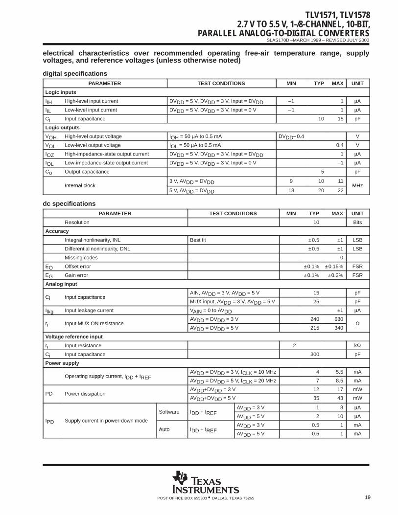
MECHANICAL DATADA (R-PDSO-G**) PLASTIC SMALL-OUTLINE PACKAGE
38 PINS SHOWN
4040066/D 11/98
0,25
0,750,50
0,15 NOM
Gage Plane
6,20NOM
8,407,80
32
11,1011,10
30
Seating Plane
10,9010,90
200,19
19
A
0,30
38
1
PINS **
A MAX
A MIN
DIM
1,20 MAX
9,60
9,80
28
M0,13
0°–8°
0,10
0,65
38
12,60
12,40
0,150,05
NOTES: A. All linear dimensions are in millimeters.B. This drawing is subject to change without notice.C. Body dimensions do not include mold flash or protrusion.D. Falls within JEDEC MO-153

TLV1571, TLV15782.7 V TO 5.5 V, 1-/8-CHANNEL, 10-BIT,PARALLEL ANALOG-TO-DIGITAL CONVERTERS
SLAS170D –MARCH 1999 – REVISED JULY 2000
28 POST OFFICE BOX 655303 • DALLAS, TEXAS 75265
MECHANICAL DATADW (R-PDSO-G**) PLASTIC SMALL-OUTLINE PACKAGE16 PINS SHOWN
4040000/C 07/96
Seating Plane
0.400 (10,15)0.419 (10,65)
0.104 (2,65) MAX
1
0.012 (0,30)0.004 (0,10)
A
8
16
0.020 (0,51)0.014 (0,35)
0.293 (7,45)0.299 (7,59)
9
0.010 (0,25)
0.050 (1,27)0.016 (0,40)
(15,24)
(15,49)
PINS **
0.010 (0,25) NOM
A MAX
DIM
A MIN
Gage Plane
20
0.500(12,70)
(12,95)0.510
(10,16)
(10,41)
0.400
0.410
16
0.600
24
0.610
(17,78)
28
0.700
(18,03)0.710
0.004 (0,10)
M0.010 (0,25)0.050 (1,27)
0°–8°
NOTES: A. All linear dimensions are in inches (millimeters).B. This drawing is subject to change without notice.C. Body dimensions do not include mold flash or protrusion not to exceed 0.006 (0,15).D. Falls within JEDEC MS-013
PACKAGING INFORMATION
Orderable Device Status (1) PackageType
PackageDrawing
Pins PackageQty
Eco Plan (2) Lead/Ball Finish MSL Peak Temp (3)
TLV1571CDW ACTIVE SOIC DW 24 25 Green (RoHS &no Sb/Br)
CU NIPDAU Level-1-260C-UNLIM
TLV1571CDWG4 ACTIVE SOIC DW 24 25 Green (RoHS &no Sb/Br)
CU NIPDAU Level-1-260C-UNLIM
TLV1571IDW ACTIVE SOIC DW 24 25 Green (RoHS &no Sb/Br)
CU NIPDAU Level-1-260C-UNLIM
TLV1571IDWG4 ACTIVE SOIC DW 24 25 Green (RoHS &no Sb/Br)
CU NIPDAU Level-1-260C-UNLIM
TLV1571IPW ACTIVE TSSOP PW 24 60 Green (RoHS &no Sb/Br)
CU NIPDAU Level-2-260C-1 YEAR
TLV1571IPWG4 ACTIVE TSSOP PW 24 60 Green (RoHS &no Sb/Br)
CU NIPDAU Level-2-260C-1 YEAR
TLV1578CDA ACTIVE TSSOP DA 32 46 Green (RoHS &no Sb/Br)
CU NIPDAU Level-2-260C-1 YEAR
TLV1578CDAG4 ACTIVE TSSOP DA 32 46 Green (RoHS &no Sb/Br)
CU NIPDAU Level-2-260C-1 YEAR
TLV1578CDAR ACTIVE TSSOP DA 32 2000 Green (RoHS &no Sb/Br)
CU NIPDAU Level-2-260C-1 YEAR
TLV1578CDARG4 ACTIVE TSSOP DA 32 2000 Green (RoHS &no Sb/Br)
CU NIPDAU Level-2-260C-1 YEAR
TLV1578IDA ACTIVE TSSOP DA 32 46 Green (RoHS &no Sb/Br)
CU NIPDAU Level-2-260C-1 YEAR
TLV1578IDAG4 ACTIVE TSSOP DA 32 46 Green (RoHS &no Sb/Br)
CU NIPDAU Level-2-260C-1 YEAR
(1) The marketing status values are defined as follows:ACTIVE: Product device recommended for new designs.LIFEBUY: TI has announced that the device will be discontinued, and a lifetime-buy period is in effect.NRND: Not recommended for new designs. Device is in production to support existing customers, but TI does not recommend using this part ina new design.PREVIEW: Device has been announced but is not in production. Samples may or may not be available.OBSOLETE: TI has discontinued the production of the device.
(2) Eco Plan - The planned eco-friendly classification: Pb-Free (RoHS), Pb-Free (RoHS Exempt), or Green (RoHS & no Sb/Br) - please checkhttp://www.ti.com/productcontent for the latest availability information and additional product content details.TBD: The Pb-Free/Green conversion plan has not been defined.Pb-Free (RoHS): TI's terms "Lead-Free" or "Pb-Free" mean semiconductor products that are compatible with the current RoHS requirementsfor all 6 substances, including the requirement that lead not exceed 0.1% by weight in homogeneous materials. Where designed to be solderedat high temperatures, TI Pb-Free products are suitable for use in specified lead-free processes.Pb-Free (RoHS Exempt): This component has a RoHS exemption for either 1) lead-based flip-chip solder bumps used between the die andpackage, or 2) lead-based die adhesive used between the die and leadframe. The component is otherwise considered Pb-Free (RoHScompatible) as defined above.Green (RoHS & no Sb/Br): TI defines "Green" to mean Pb-Free (RoHS compatible), and free of Bromine (Br) and Antimony (Sb) based flameretardants (Br or Sb do not exceed 0.1% by weight in homogeneous material)
(3) MSL, Peak Temp. -- The Moisture Sensitivity Level rating according to the JEDEC industry standard classifications, and peak soldertemperature.
Important Information and Disclaimer:The information provided on this page represents TI's knowledge and belief as of the date that it isprovided. TI bases its knowledge and belief on information provided by third parties, and makes no representation or warranty as to theaccuracy of such information. Efforts are underway to better integrate information from third parties. TI has taken and continues to takereasonable steps to provide representative and accurate information but may not have conducted destructive testing or chemical analysis onincoming materials and chemicals. TI and TI suppliers consider certain information to be proprietary, and thus CAS numbers and other limitedinformation may not be available for release.
PACKAGE OPTION ADDENDUM
www.ti.com 12-Sep-2006
Addendum-Page 1

In no event shall TI's liability arising out of such information exceed the total purchase price of the TI part(s) at issue in this document sold by TIto Customer on an annual basis.
PACKAGE OPTION ADDENDUM
www.ti.com 12-Sep-2006
Addendum-Page 2

TAPE AND REEL INFORMATION
*All dimensions are nominal
Device PackageType
PackageDrawing
Pins SPQ ReelDiameter
(mm)
ReelWidth
W1 (mm)
A0 (mm) B0 (mm) K0 (mm) P1(mm)
W(mm)
Pin1Quadrant
TLV1578CDAR TSSOP DA 32 2000 330.0 24.4 8.6 11.5 1.6 12.0 24.0 Q1
PACKAGE MATERIALS INFORMATION
www.ti.com 19-Mar-2008
Pack Materials-Page 1

*All dimensions are nominal
Device Package Type Package Drawing Pins SPQ Length (mm) Width (mm) Height (mm)
TLV1578CDAR TSSOP DA 32 2000 346.0 346.0 41.0
PACKAGE MATERIALS INFORMATION
www.ti.com 19-Mar-2008
Pack Materials-Page 2

IMPORTANT NOTICETexas Instruments Incorporated and its subsidiaries (TI) reserve the right to make corrections, modifications, enhancements, improvements,and other changes to its products and services at any time and to discontinue any product or service without notice. Customers shouldobtain the latest relevant information before placing orders and should verify that such information is current and complete. All products aresold subject to TI’s terms and conditions of sale supplied at the time of order acknowledgment.TI warrants performance of its hardware products to the specifications applicable at the time of sale in accordance with TI’s standardwarranty. Testing and other quality control techniques are used to the extent TI deems necessary to support this warranty. Except wheremandated by government requirements, testing of all parameters of each product is not necessarily performed.TI assumes no liability for applications assistance or customer product design. Customers are responsible for their products andapplications using TI components. To minimize the risks associated with customer products and applications, customers should provideadequate design and operating safeguards.TI does not warrant or represent that any license, either express or implied, is granted under any TI patent right, copyright, mask work right,or other TI intellectual property right relating to any combination, machine, or process in which TI products or services are used. Informationpublished by TI regarding third-party products or services does not constitute a license from TI to use such products or services or awarranty or endorsement thereof. Use of such information may require a license from a third party under the patents or other intellectualproperty of the third party, or a license from TI under the patents or other intellectual property of TI.Reproduction of TI information in TI data books or data sheets is permissible only if reproduction is without alteration and is accompaniedby all associated warranties, conditions, limitations, and notices. Reproduction of this information with alteration is an unfair and deceptivebusiness practice. TI is not responsible or liable for such altered documentation. Information of third parties may be subject to additionalrestrictions.Resale of TI products or services with statements different from or beyond the parameters stated by TI for that product or service voids allexpress and any implied warranties for the associated TI product or service and is an unfair and deceptive business practice. TI is notresponsible or liable for any such statements.TI products are not authorized for use in safety-critical applications (such as life support) where a failure of the TI product would reasonablybe expected to cause severe personal injury or death, unless officers of the parties have executed an agreement specifically governingsuch use. Buyers represent that they have all necessary expertise in the safety and regulatory ramifications of their applications, andacknowledge and agree that they are solely responsible for all legal, regulatory and safety-related requirements concerning their productsand any use of TI products in such safety-critical applications, notwithstanding any applications-related information or support that may beprovided by TI. Further, Buyers must fully indemnify TI and its representatives against any damages arising out of the use of TI products insuch safety-critical applications.TI products are neither designed nor intended for use in military/aerospace applications or environments unless the TI products arespecifically designated by TI as military-grade or "enhanced plastic." Only products designated by TI as military-grade meet militaryspecifications. Buyers acknowledge and agree that any such use of TI products which TI has not designated as military-grade is solely atthe Buyer's risk, and that they are solely responsible for compliance with all legal and regulatory requirements in connection with such use.TI products are neither designed nor intended for use in automotive applications or environments unless the specific TI products aredesignated by TI as compliant with ISO/TS 16949 requirements. Buyers acknowledge and agree that, if they use any non-designatedproducts in automotive applications, TI will not be responsible for any failure to meet such requirements.Following are URLs where you can obtain information on other Texas Instruments products and application solutions:Products ApplicationsAmplifiers amplifier.ti.com Audio www.ti.com/audioData Converters dataconverter.ti.com Automotive www.ti.com/automotiveDSP dsp.ti.com Broadband www.ti.com/broadbandClocks and Timers www.ti.com/clocks Digital Control www.ti.com/digitalcontrolInterface interface.ti.com Medical www.ti.com/medicalLogic logic.ti.com Military www.ti.com/militaryPower Mgmt power.ti.com Optical Networking www.ti.com/opticalnetworkMicrocontrollers microcontroller.ti.com Security www.ti.com/securityRFID www.ti-rfid.com Telephony www.ti.com/telephonyRF/IF and ZigBee® Solutions www.ti.com/lprf Video & Imaging www.ti.com/video
Wireless www.ti.com/wireless
Mailing Address: Texas Instruments, Post Office Box 655303, Dallas, Texas 75265Copyright © 2008, Texas Instruments Incorporated