Embed Size (px)
Citation preview
2.7 V to 5.5 V, 140 μA, Rail-to-Rail Output 12-Bit DAC in an SOT-23
AD5320
Rev. C Information furnished by Analog Devices is believed to be accurate and reliable. However, no responsibility is assumed by Analog Devices for its use, nor for any infringements of patents or other rights of third parties that may result from its use. Specifications subject to change without notice. No license is granted by implication or otherwise under any patent or patent rights of Analog Devices. Trademarks and registered trademarks are the property of their respective owners.
One Technology Way, P.O. Box 9106, Norwood, MA 02062-9106, U.S.A.Tel: 781.329.4700 www.analog.com Fax: 781.461.3113 © 2005 Analog Devices, Inc. All rights reserved.
FEATURES Single 12-bit DAC 6-lead SOT-23 and 8-lead MSOP packages Micropower operation: 140 μA @ 5 V Power-down to 200 nA @ 5 V, 50 nA @ 3 V 2.7 V to 5.5 V power supply Guaranteed monotonic by design Reference derived from power supply Power-on reset to zero volts Three power-down functions Low power serial interface with Schmitt-triggered inputs On-chip output buffer amplifier, rail-to-rail operation SYNC interrupt facility
APPLICATIONS Portable battery-powered instruments Digital gain and offset adjustment Programmable voltage and current sources Programmable attenuators
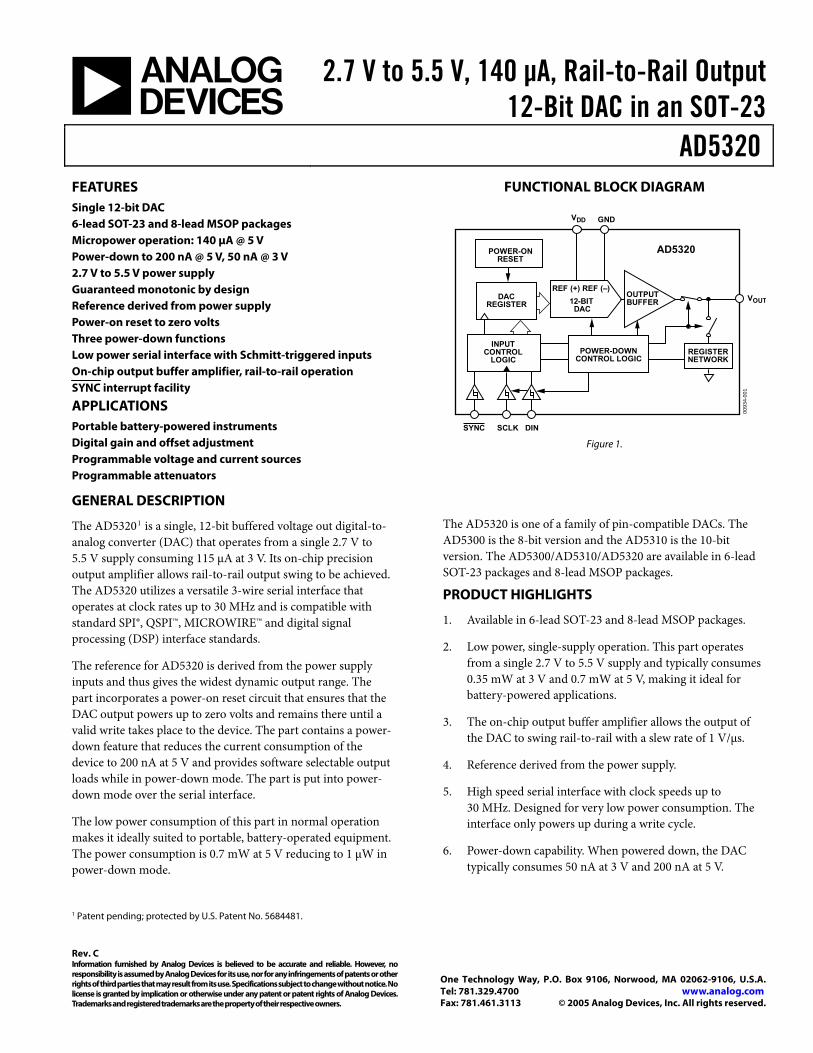
FUNCTIONAL BLOCK DIAGRAM
VDD
VOUT
GND
AD5320
12-BITDAC
SCLK DIN
REF (+) REF (–)
REGISTERNETWORK
POWER-DOWNCONTROL LOGIC
DACREGISTER
OUTPUTBUFFER
POWER-ONRESET
SYNC
INPUTCONTROL
LOGIC
0093
4-00
1
Figure 1.
GENERAL DESCRIPTION
The AD53201 is a single, 12-bit buffered voltage out digital-to-analog converter (DAC) that operates from a single 2.7 V to 5.5 V supply consuming 115 μA at 3 V. Its on-chip precision output amplifier allows rail-to-rail output swing to be achieved. The AD5320 utilizes a versatile 3-wire serial interface that operates at clock rates up to 30 MHz and is compatible with standard SPI®, QSPI™, MICROWIRE™ and digital signal processing (DSP) interface standards.
The reference for AD5320 is derived from the power supply inputs and thus gives the widest dynamic output range. The part incorporates a power-on reset circuit that ensures that the DAC output powers up to zero volts and remains there until a valid write takes place to the device. The part contains a power-down feature that reduces the current consumption of the device to 200 nA at 5 V and provides software selectable output loads while in power-down mode. The part is put into power-down mode over the serial interface.
The low power consumption of this part in normal operation makes it ideally suited to portable, battery-operated equipment. The power consumption is 0.7 mW at 5 V reducing to 1 μW in power-down mode.
1 Patent pending; protected by U.S. Patent No. 5684481.
The AD5320 is one of a family of pin-compatible DACs. The AD5300 is the 8-bit version and the AD5310 is the 10-bit version. The AD5300/AD5310/AD5320 are available in 6-lead SOT-23 packages and 8-lead MSOP packages.
PRODUCT HIGHLIGHTS
1. Available in 6-lead SOT-23 and 8-lead MSOP packages.
2. Low power, single-supply operation. This part operates from a single 2.7 V to 5.5 V supply and typically consumes 0.35 mW at 3 V and 0.7 mW at 5 V, making it ideal for battery-powered applications.
3. The on-chip output buffer amplifier allows the output of the DAC to swing rail-to-rail with a slew rate of 1 V/μs.
4. Reference derived from the power supply.
5. High speed serial interface with clock speeds up to 30 MHz. Designed for very low power consumption. The interface only powers up during a write cycle.
6. Power-down capability. When powered down, the DAC typically consumes 50 nA at 3 V and 200 nA at 5 V.
AD5320
Rev. C | Page 2 of 20
TABLE OF CONTENTS Features .............................................................................................. 1
Applications....................................................................................... 1
Functional Block Diagram .............................................................. 1
General Description ......................................................................... 1
Product Highlights ........................................................................... 1
Revision History ............................................................................... 2
Specifications..................................................................................... 3
Timing Characteristics ................................................................ 4
Absolute Maximum Ratings............................................................ 5
ESD Caution.................................................................................. 5
Pin Configurations and Function Descriptions ........................... 6
Terminology ...................................................................................... 7
Typical Performance Characteristics ............................................. 8
Theory of Operation ...................................................................... 11
D/A Section................................................................................. 11
Resistor String ............................................................................. 11
Output Amplifier........................................................................ 11
Serial Interface ................................................................................ 12
Input Shift Register .................................................................... 12
SYNC Interrupt .......................................................................... 12
Power-On Reset .......................................................................... 12
Power-Down Modes .................................................................. 13
Microprocessor Interfacing........................................................... 14
AD5320 to ADSP-2101/ADSP-2103 Interface ....................... 14
AD5320 to 68HC11/68L11 Interface....................................... 14
AD5320 to 80C51/80L51 Interface .......................................... 14
AD5320 to MICROWIRE Interface......................................... 14
Applications..................................................................................... 15
Using REF19x as a Power Supply for AD5320 ....................... 15
Bipolar Operation Using the AD5320 ..................................... 15
Using AD5320 with an Opto-Isolated Interface .................... 15
Power Supply Bypassing and Grounding................................ 16
Outline Dimensions ....................................................................... 17
Ordering Guide .......................................................................... 17
REVISION HISTORY
11/05—Rev. B to Rev. C Updated Format..................................................................Universal Changes to Table 4............................................................................ 6 Updated Outline Dimensions ....................................................... 17 Changes to Ordering Guide .......................................................... 17
AD5320
Rev. C | Page 3 of 20
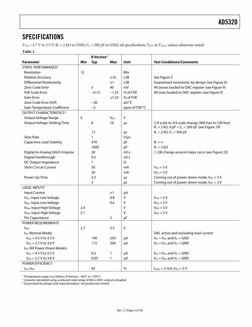
SPECIFICATIONS VDD = 2.7 V to 5.5 V; RL = 2 kΩ to GND; CL = 200 pF to GND; all specifications TMIN to TMAX, unless otherwise noted.
Table 1. B Version1 Parameter Min Typ Max Unit Test Conditions/Comments STATIC PERFORMANCE2
Resolution 12 Bits Relative Accuracy ±16 LSB See Figure 5Differential Nonlinearity ±1 LSB Guaranteed monotonic by design (see Figure 6) Zero-Code Error 5 40 mV All zeroes loaded to DAC register (see Figure 9) Full-Scale Error −0.15 −1.25 % of FSR All ones loaded to DAC register (see Figure 9) Gain Error ±1.25 % of FSR Zero-Code Error Drift −20 μV/°C Gain Temperature Coefficient −5 ppm of FSR/°C
OUTPUT CHARACTERISTICS3 Output Voltage Range 0 VDD V Output Voltage Settling Time 8 10 μs 1/4 scale to 3/4 scale change (400 hex to C00 hex)
RL = 2 kΩ, 0 pF < CL < 200 pF (see Figure 19) 12 μs RL = 2 kΩ, CL = 500 pF Slew Rate 1 V/μs Capacitive Load Stability 470 pF RL = ∞ 1000 pF RL = 2 kΩ Digital-to-Analog Glitch Impulse 20 nV-s 1 LSB change around major carry (see Figure 22) Digital Feedthrough 0.5 nV-s DC Output Impedance 1 Ω Short Circuit Current 50 mA VDD = 5 V 20 mA VDD = 3 V Power-Up Time 2.5 μs Coming out of power-down mode, VDD = 5 V 5 μs Coming out of power-down mode, VDD = 3 V
LOGIC INPUTS3 Input Current ±1 μA VINL, Input Low Voltage 0.8 V VDD = 5 V VINL, Input Low Voltage 0.6 V VDD = 3 V VINH, Input High Voltage 2.4 V VDD = 5 V VINH, Input High Voltage 2.1 V VDD = 3 V Pin Capacitance 3 pF
POWER REQUIREMENTS VDD 2.7 5.5 V IDD (Normal Mode) DAC active and excluding load current
VDD = 4.5 V to 5.5 V 140 250 μA VIH = VDD and VIL = GND VDD = 2.7 V to 3.6 V 115 200 μA VIH = VDD and VIL = GND
IDD (All Power-Down Modes) VDD = 4.5 V to 5.5 V 0.2 1 μA VIH = VDD and VIL = GND VDD = 2.7 V to 3.6 V 0.05 1 μA VIH = VDD and VIL = GND
POWER EFFICIENCY IOUT/IDD 93 % ILOAD = 2 mA, VDD = 5 V
1 Temperature range is as follows: B Version: −40°C to +105°C. 2 Linearity calculated using a reduced code range of 48 to 4047; output unloaded. 3 Guaranteed by design and characterization, not production tested.
AD5320
Rev. C | Page 4 of 20
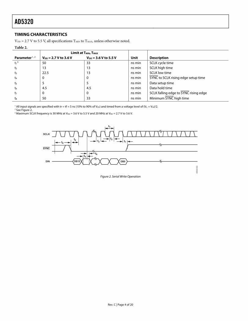
TIMING CHARACTERISTICS VDD = 2.7 V to 5.5 V, all specifications TMIN to TMAX, unless otherwise noted.
Table 2. Limit at TMIN, TMAX Parameter1, 2 VDD = 2.7 V to 3.6 V VDD = 3.6 V to 5.5 V Unit Description t1
3 50 33 ns min SCLK cycle time t2 13 13 ns min SCLK high time t3 22.5 13 ns min SCLK low time t4 0 0 ns min SYNC to SCLK rising edge setup time
t5 5 5 ns min Data setup time t6 4.5 4.5 ns min Data hold time t7 0 0 ns min SCLK falling edge to SYNC rising edge
t8 50 33 ns min Minimum SYNC high time 1 All input signals are specified with tr = tf = 5 ns (10% to 90% of VDD) and timed from a voltage level of (VIL + VIH)/2. 2 See Figure 2. 3 Maximum SCLK frequency is 30 MHz at VDD = 3.6 V to 5.5 V and 20 MHz at VDD = 2.7 V to 3.6 V.
0093
4-00
2
SCLK
DIN DB15 DB0
t4
t1
t3t2
t8t7
t6t5
SYNC
Figure 2. Serial Write Operation
AD5320
Rev. C | Page 5 of 20
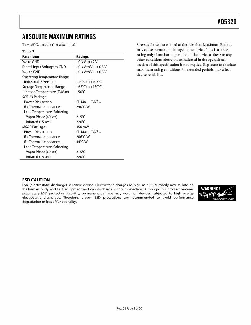
ABSOLUTE MAXIMUM RATINGSTA = 25°C, unless otherwise noted.
Table 3. Parameter Ratings VDD to GND −0.3 V to +7 V Digital Input Voltage to GND −0.3 V to VDD + 0.3 V VOUT to GND −0.3 V to VDD + 0.3 V Operating Temperature Range
Industrial (B Version) −40°C to +105°C Storage Temperature Range −65°C to +150°C Junction Temperature (TJ Max) 150°C SOT-23 Package
Power Dissipation (TJ Max − TA)/θJA θJA Thermal Impedance 240°C/W Lead Temperature, Soldering
Vapor Phase (60 sec) 215°C Infrared (15 sec) 220°C
MSOP Package 450 mW Power Dissipation (TJ Max − TA)/θJA θJA Thermal Impedance 206°C/W θJC Thermal Impedance 44°C/W Lead Temperature, Soldering
Vapor Phase (60 sec) 215°C Infrared (15 sec) 220°C
Stresses above those listed under Absolute Maximum Ratings may cause permanent damage to the device. This is a stress rating only; functional operation of the device at these or any other conditions above those indicated in the operational section of this specification is not implied. Exposure to absolute maximum rating conditions for extended periods may affect device reliability.
ESD CAUTION ESD (electrostatic discharge) sensitive device. Electrostatic charges as high as 4000 V readily accumulate on the human body and test equipment and can discharge without detection. Although this product features proprietary ESD protection circuitry, permanent damage may occur on devices subjected to high energy electrostatic discharges. Therefore, proper ESD precautions are recommended to avoid performance degradation or loss of functionality.
AD5320
Rev. C | Page 6 of 20
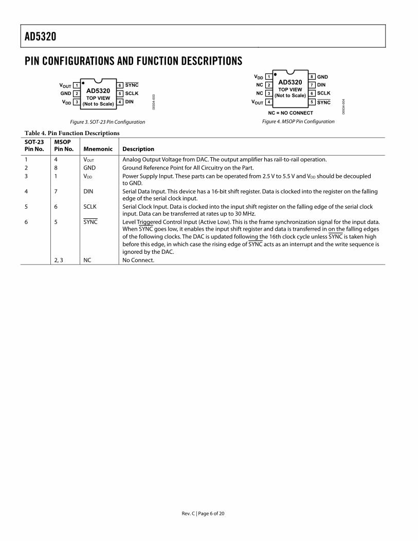
PIN CONFIGURATIONS AND FUNCTION DESCRIPTIONS
AD5320TOP VIEW
(Not to Scale)
VOUT 1
GND 2
VDD 3
SYNC
SCLKDIN
6
5
4
0093
4-00
3
Figure 3. SOT-23 Pin Configuration
AD5320TOP VIEW
(Not to Scale)
VDD 1
NC 2
NC 3
VOUT 4 SYNC
SCLKDINGND8
7
6
5
0093
4-00
4
NC = NO CONNECT Figure 4. MSOP Pin Configuration
Table 4. Pin Function Descriptions SOT-23 Pin No.
MSOP Pin No.
Mnemonic
Description
1 4 VOUT Analog Output Voltage from DAC. The output amplifier has rail-to-rail operation. 2 8 GND Ground Reference Point for All Circuitry on the Part. 3 1 VDD Power Supply Input. These parts can be operated from 2.5 V to 5.5 V and VDD should be decoupled
to GND. 4 7 DIN Serial Data Input. This device has a 16-bit shift register. Data is clocked into the register on the falling
edge of the serial clock input. 5 6 SCLK Serial Clock Input. Data is clocked into the input shift register on the falling edge of the serial clock
input. Data can be transferred at rates up to 30 MHz. 6 5 SYNC Level Triggered Control Input (Active Low). This is the frame synchronization signal for the input data.
When SYNC goes low, it enables the input shift register and data is transferred in on the falling edges of the following clocks. The DAC is updated following the 16th clock cycle unless SYNC is taken high before this edge, in which case the rising edge of SYNC acts as an interrupt and the write sequence is ignored by the DAC.
2, 3 NC No Connect.

AD5320
Rev. C | Page 7 of 20
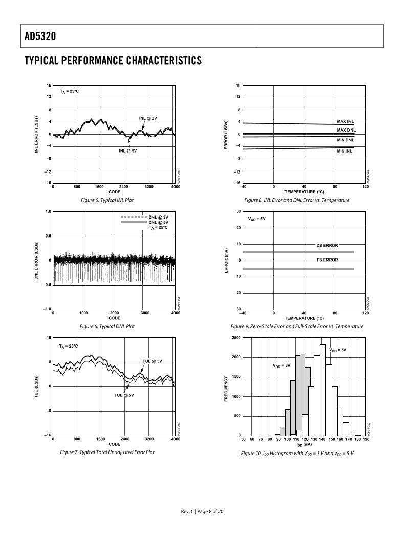
TERMINOLOGY Relative Accuracy For the DAC, relative accuracy or integral nonlinearity (INL) is a measure of the maximum deviation, in LSBs, from a straight line passing through the endpoints of the DAC transfer function. A typical INL vs. code plot can be seen in Figure 5.
Differential Nonlinearity Differential nonlinearity (DNL) is the difference between the measured change and the ideal 1 LSB change between any two adjacent codes. A specified differential nonlinearity of ±1 LSB maximum ensures monotonicity. This DAC is guaranteed monotonic by design. A typical DNL vs. code plot can be seen in Figure 6.
Zero-Code Error Zero-code error is a measure of the output error when zero code (000 hex) is loaded to the DAC register. Ideally, the output should be 0 V. The zero-code error is always positive in the AD5320 because the output of the DAC cannot go below 0 V due to a combination of the offset errors in the DAC and output amplifier. Zero-code error is expressed in mV. A plot of zero-code error vs. temperature can be seen in Figure 9.
Full-Scale Error Full-scale error is a measure of the output error when full-scale code (FFF Hex) is loaded to the DAC register. Ideally the output should be VDD − 1 LSB. Full-scale error is expressed in percent of full-scale range. A plot of full-scale error vs. temperature can be seen in Figure 9.
Gain Error This is a measure of the span error of the DAC. It is the deviation in slope of the DAC transfer characteristic from ideal expressed as a percent of the full-scale range.
Total Unadjusted Error Total unadjusted error (TUE) is a measure of the output error considering all the various errors. A typical TUE vs. code plot can be seen in Figure 7.
Zero-Code Error Drift This is a measure of the change in zero-code error with a change in temperature. It is expressed in μV/°C.
Gain Error Drift This is a measure of the change in gain error with changes in temperature. It is expressed in (ppm of full-scale range)/°C.
Digital-to-Analog Glitch Impulse Digital-to-analog glitch impulse is the impulse injected into the analog output when the input code in the DAC register changes state. It is normally specified as the area of the glitch in nV seconds and is measured when the digital input code is changed by 1 LSB at the major carry transition (7FF Hex to 800 Hex); see Figure 22.
Digital Feedthrough Digital feedthrough is a measure of the impulse injected into the analog output of the DAC from the digital inputs of the DAC but is measured when the DAC output is not updated. It is specified in nV seconds and measured with a full-scale code change on the data bus, that is, from all 0s to all 1s and vice versa.
AD5320
Rev. C | Page 8 of 20
TYPICAL PERFORMANCE CHARACTERISTICS
INL @ 5V
INL @ 3V
CODE
INL
ERR
OR
(LSB
s)
16
12
4
–4
–12
8
0
–8
–160 800 1600 2400 40003200
0093
4-00
5
TA = 25°C
Figure 5. Typical INL Plot
CODE
DN
L ER
RO
R (L
SBs)
1.0
0.5
0
–0.5
–1.00 1000 2000 3000 4000
0093
4-00
6
DNL @ 3VDNL @ 5VTA = 25°C
Figure 6. Typical DNL Plot
CODE
TUE
(LSB
s)
16
8
0
–8
–160 800 1600 2400 40003200
0093
4-00
7
TUE @ 3V
TUE @ 5V
TA = 25°C
Figure 7. Typical Total Unadjusted Error Plot
MAX INL
MAX DNL
MIN INL
MIN DNL
TEMPERATURE (°C)–40 0 40 80 120
0093
4-00
8
16
12
4
–4
–12
8
0
–8
–16
ERR
OR
(LSB
s)
Figure 8. INL Error and DNL Error vs. Temperature
VDD = 5V
ZS ERROR
FS ERROR
30
20
30
0
10
20
10
TEMPERATURE (°C)
ERR
OR
(mV)
–40 0 40 80 120
0093
4-00
9
Figure 9. Zero-Scale Error and Full-Scale Error vs. Temperature
2500
2000
500
50 190
1500
1000
0
FREQ
UEN
CY
VDD = 3V
VDD = 5V
60 70 80 90 100 110 120 130 140 150 160 170 180
0093
4-01
0
IDD (µA) Figure 10. IDD Histogram with VDD = 3 V and VDD = 5 V

AD5320
Rev. C | Page 9 of 20
DAC LOADED WITH FFF HEX
DAC LOADED WITH 000 HEX
ISOURCE/SINK (mA)
V OU
T (V
)
3
2
1
00 5 10
0093
4-01
1
TA = 25°C
15
Figure 11. Source and Sink Current Capability with VDD = 3 V
5
4
3
2
1DAC LOADED WITH 000 HEX
DAC LOADED WITH FFF HEX
ISOURCE/SINK (mA)
V OU
T (V
)
00 5 10
0093
4-01
2
15
TA = 25°C
Figure 12. Source and Sink Current Capability with VDD = 5 V
CODE
I DD
(µA
)
0 800 1600 2400 3200 4000
0093
4-01
3
500
400
0
300
200
100
VDD = 5V
VDD = 3V
Figure 13. Supply Current vs. Code
TEMPERATURE °C
I DD
(µA
)
300
200
150
50
0–40 0 40 80 120
0093
4-01
4
VDD = 5V
Figure 14. Supply Current vs. Temperature
VDD (V)2.7 3.2 3.73.7 4.2 4.7 5
0093
4-01
5
300
250
200
150
100
50
0
I DD
(µA
)
TA = 25°C
Figure 15. Supply Current vs. Supply Voltage
2.7 3.2 3.7 4.7 5.24.2
0093
4-01
6
1.0
0.9
0
0.4
0.3
0.2
0.1
0.8
0.6
0.7
0.5
–40°C
CONDITIONTHREE-STATE
VDD (V)
I DD
(µA
)
+25°C
+105°C
Figure 16. Power-Down Current vs. Supply Voltage
AD5320
Rev. C | Page 10 of 20
TA = 25°C
VDD = 5V
VLOGIC (V)
I DD
(µA
)
800
600
400
200
00 54321
0093
4-01
7VDD = 3V
Figure 17. Supply Current vs. Logic Input Voltage
VOUT
CLK
CH1 1V, CH2 5V, TIME BASE = 1µs/DIV
CH2
CH1
0093
4-01
8
VDD = 5VFULL-SCALE CODE CHANGE000 HEX – FFF HEXTA = 25°COUTPUT LOADED WITH2kΩ AND 200pF TO GND
Figure 18. Full-Scale Settling Time
VOUT
CLK
CH1 1V, CH2 5V, TIME BASE = 1µs/DIV
0093
4-01
9
CH1
CH2 VDD = 5VHALF-SCALE CODE CHANGE400 HEX – C00 HEXTA = 25°COUTPUT LOADED WITH2kΩ AND 200pF TO GND
Figure 19. Half-Scale Settling Time
CH1
CH2
CH1 1V, CH 2 1V, TIME BASE = 20µs/DIV
0093
4-02
0
2kΩ LOAD TO VDD
VDD
VOUT
Figure 20. Power-On Reset to 0 V
CH1 1V, CH2 5V, TIME BASE = 5µs/DIV
0093
4-02
1
CH2
CH1
CLK
VOUT
VDD = 5V
Figure 21. Exiting Power-Down (800 Hex Loaded)
LOADED WITH 2kΩAND 200pF TO GND
CODE CHANGE:800 HEX TO 7FF HEX
500ns/DIV
V OU
T (V
)
0093
4-02
2
2.54
2.52
2.50
2.48
2.46
2.56
Figure 22. Digital-to-Analog Glitch Impulse
AD5320
Rev. C | Page 11 of 20
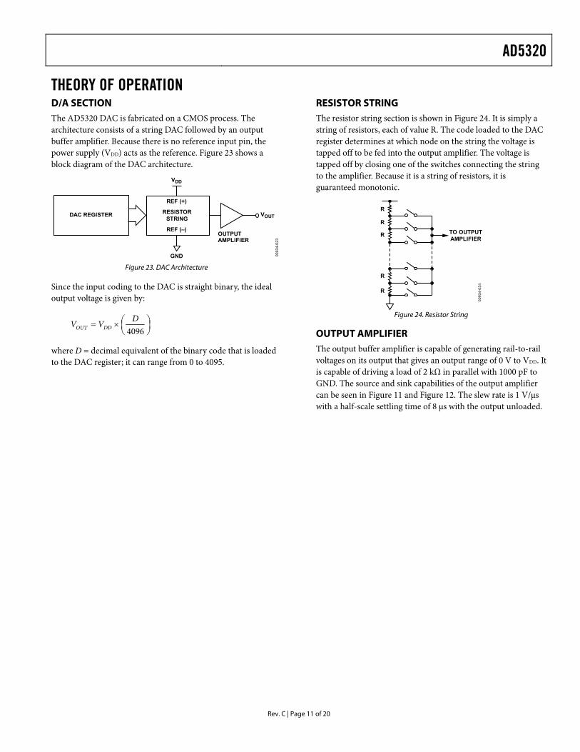
THEORY OF OPERATIOND/A SECTION The AD5320 DAC is fabricated on a CMOS process. The architecture consists of a string DAC followed by an output buffer amplifier. Because there is no reference input pin, the power supply (VDD) acts as the reference. Figure 23 shows a block diagram of the DAC architecture.
VDD
VOUT
GND
RESISTORSTRING
REF (+)
REF (–)OUTPUTAMPLIFIER
DAC REGISTER
0093
4-02
3
Figure 23. DAC Architecture
Since the input coding to the DAC is straight binary, the ideal output voltage is given by:
⎟⎠⎞
⎜⎝⎛×=
4096DVV DDOUT
where D = decimal equivalent of the binary code that is loaded to the DAC register; it can range from 0 to 4095.
RESISTOR STRING The resistor string section is shown in Figure 24. It is simply a string of resistors, each of value R. The code loaded to the DAC register determines at which node on the string the voltage is tapped off to be fed into the output amplifier. The voltage is tapped off by closing one of the switches connecting the string to the amplifier. Because it is a string of resistors, it is guaranteed monotonic.
R
R
R
R
R
TO OUTPUTAMPLIFIER
0093
4-02
4
Figure 24. Resistor String
OUTPUT AMPLIFIER The output buffer amplifier is capable of generating rail-to-rail voltages on its output that gives an output range of 0 V to VDD. It is capable of driving a load of 2 kΩ in parallel with 1000 pF to GND. The source and sink capabilities of the output amplifier can be seen in Figure 11 and Figure 12. The slew rate is 1 V/μs with a half-scale settling time of 8 μs with the output unloaded.
AD5320
Rev. C | Page 12 of 20
SERIAL INTERFACEThe AD5320 has a 3-wire serial interface (SYNC, SCLK, and DIN) that is compatible with SPI®, QSPITM, and MICROWIRETM interface standards as well as most DSPs. See Figure 2 for a timing diagram of a typical write sequence.
The write sequence begins by bringing the SYNC line low. Data from the DIN line is clocked into the 16-bit shift register on the falling edge of SCLK. The serial clock frequency can be as high as 30 MHz, making the AD5320 compatible with high speed DSPs. On the 16th falling clock edge, the last data bit is clocked in and the programmed function is executed (that is, a change in DAC register contents and/or a change in the mode of operation). At this stage, the SYNC line can be kept low or be brought high. In either case, it must be brought high for a minimum of 33 ns before the next write sequence so that a falling edge of SYNC can initiate the next write sequence. Because the SYNC buffer draws more current when VIN = 2.4 V than it does when VIN = 0.8 V, SYNC should be idled low between write sequences for even lower power operation of the part. As previously mentioned, SYNC must be brought high again just before the next write sequence.
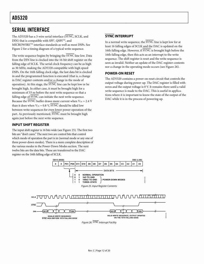
INPUT SHIFT REGISTER The input shift register is 16 bits wide (see Figure 25). The first two bits are “don’t cares.” The next two are control bits that control which mode of operation the part is in (normal mode or any one of three power-down modes). There is a more complete description of the various modes in the Power-Down Modes section. The next twelve bits are the data bits. These are transferred to the DAC register on the 16th falling edge of SCLK.
SYNC INTERRUPT
In a normal write sequence, the SYNC line is kept low for at least 16 falling edges of SCLK and the DAC is updated on the 16th falling edge. However, if SYNC is brought high before the 16th falling edge, then this acts as an interrupt to the write sequence. The shift register is reset and the write sequence is seen as invalid. Neither an update of the DAC register contents nor a change in the operating mode occurs (see Figure 26).
POWER-ON RESET The AD5320 contains a power-on reset circuit that controls the output voltage during power-up. The DAC register is filled with zeros and the output voltage is 0 V. It remains there until a valid write sequence is made to the DAC. This is useful in applica-tions where it is important to know the state of the output of the DAC while it is in the process of powering up.
DB15 (MSB) DB0 (LSB)
X PD0 D11 D10 D9 D8 D7 D6 D5 D4PD1X D3 D2 D1 D0
DATA BITS
0093
4-02
5
0011
0101
NORMAL OPERATION1kΩ TO GND100kΩ TO GNDTHREE–STATE
POWER-DOWN MODES
Figure 25. Input Register Contents
DB15 DB0 DB15
SCLK
SYNC
DIN
INVALID WRITE SEQUENCE:SYNC HIGH BEFORE 16TH FALLING EDGE
VALID WRITE SEQUENCE, OUTPUT UPDATESON THE 16TH FALLING EDGE
DB0
0093
4-02
8
Figure 26. SYNC Interrupt Facility
AD5320
Rev. C | Page 13 of 20
POWER-DOWN MODES The AD5320 contains four separate modes of operation. These modes are software-programmable by setting two bits (DB13 and DB12) in the control register. Table 5 shows how the state of the bits corresponds to the mode of operation of the device.
Table 5. Modes of Operation for the AD5320 DB13 DB12 Operating Mode 0 0 Normal Operation Power-Down Modes 0 1 1 kΩ to GND 1 0 100 kΩ to GND 1 1 Three-State
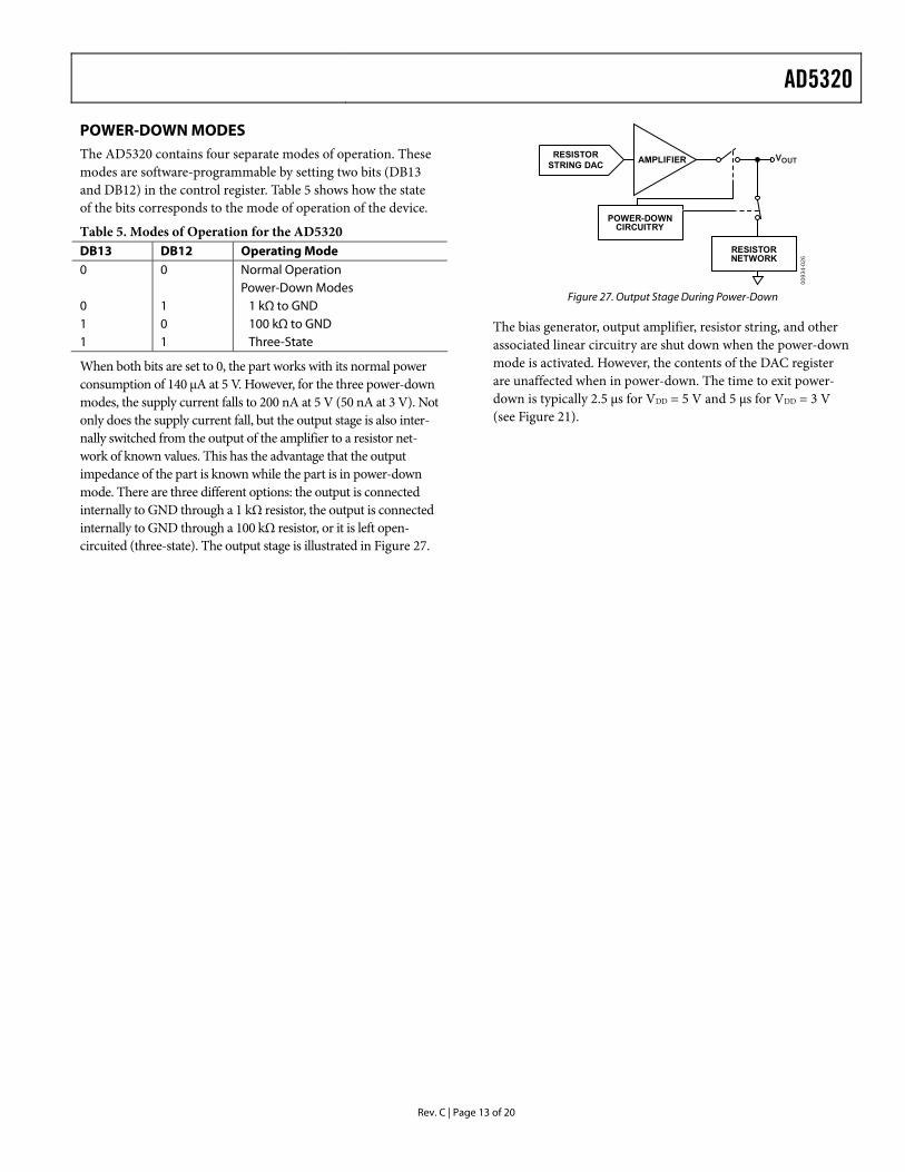
When both bits are set to 0, the part works with its normal power consumption of 140 μA at 5 V. However, for the three power-down modes, the supply current falls to 200 nA at 5 V (50 nA at 3 V). Not only does the supply current fall, but the output stage is also inter-nally switched from the output of the amplifier to a resistor net-work of known values. This has the advantage that the output impedance of the part is known while the part is in power-down mode. There are three different options: the output is connected internally to GND through a 1 kΩ resistor, the output is connected internally to GND through a 100 kΩ resistor, or it is left open-circuited (three-state). The output stage is illustrated in Figure 27.
RESISTORSTRING DAC
RESISTORNETWORK
POWER-DOWNCIRCUITRY
VOUT
0093
4-02
6
AMPLIFIER
Figure 27. Output Stage During Power-Down
The bias generator, output amplifier, resistor string, and other associated linear circuitry are shut down when the power-down mode is activated. However, the contents of the DAC register are unaffected when in power-down. The time to exit power-down is typically 2.5 μs for VDD = 5 V and 5 μs for VDD = 3 V (see Figure 21).

AD5320
Rev. C | Page 14 of 20
MICROPROCESSOR INTERFACINGAD5320 TO ADSP-2101/ADSP-2103 INTERFACE Figure 28 shows a serial interface between the AD5320 and the ADSP-2101/ADSP-2103. The ADSP-2101/ADSP-2103 should be set up to operate in the serial port (SPORT) transmit alter-nate framing mode. The ADSP-2101/ADSP-2103 SPORT are programmed through the SPORT control register and should be configured as follows: internal clock operation, active low framing, and 16-bit word length. Transmission is initiated by writing a word to the Tx register after the SPORT has been enabled.
AD5320 TO 68HC11/68L11 INTERFACE Figure 29 shows a serial interface between the AD5320 and the 68HC11/68L11 microcontroller. SCK of the 68HC11/68L11 drives the SCLK of the AD5320, while the MOSI output drives the serial data line of the DAC. The SYNC signal is derived from a port line (PC7). For correct operation of this interface, the 68HC11/68L11 should be configured so that the CPOL bit is a 0 and the CPHA bit is a 1. When data is being transmitted to the DAC, the SYNC line is taken low (PC7). When the 68HC11/68L11 are configured, data appearing on the MOSI output is valid on the falling edge of SCK as shown in Figure 29.
Serial data from the 68HC11/68L11 is transmitted in 8-bit bytes with only eight falling clock edges occurring in the transmit cycle. Data is transmitted MSB first. In order to load data to the AD5320, PC7 is left low after the first eight bits are transferred, and a second serial write operation is performed to the DAC and PC7 is taken high at the end of this procedure.
DIN
SCLK
SYNCPC7
SCK
MOSI
68HC11/68L11*
*ADDITIONAL PINS OMITTED FOR CLARITY 0093
4-02
9
AD5320*
Figure 29. AD5320 to 68HC11/68L11 Interface
AD5320 TO 80C51/80L51 INTERFACE Figure 30 shows a serial interface between the AD5320 and the 80C51/80L51 microcontrollers. TXD of the 80C51/80L51 drives SCLK of the AD5320, while RXD drives the serial data line of the part. The SYNC signal is again derived from a bit programmable pin on the port. In this case, port line P3.3 is used. When data is to be transmitted to the AD5320, P3.3 is taken low. The 80C51/80L51 transmits data only in 8-bit bytes; thus only eight falling clock edges occur in the transmit cycle. To load data to the DAC, P3.3 is left low after the first eight bits are transmitted, and a second write cycle is initiated to transmit the second byte of data. P3.3 is taken high following the completion of this cycle. The 80C51/ 80L51 output the serial data in a format that has the LSB first. The AD5320 requires its data with the MSB as the first bit received. The 80C51/80L51 transmit routine should consider this.
DIN
SCLK
SYNCP3.3
TXD
RXD
80C51/80L51*
*ADDITIONAL PINS OMITTED FOR CLARITY 0093
4-03
0
AD5320*
Figure 30. AD5320 to 80C51/80L51 Interface
AD5320 TO MICROWIRE INTERFACE Figure 31 shows an interface between the AD5320 and any MICROWIRE-compatible device. Serial data is shifted out on the falling edge of the serial clock and is clocked into the AD5320 on the rising edge of the SK.
DIN
SCLK
SYNCCS
SK
SO
MICROWIRE*
*ADDITIONAL PINS OMITTED FOR CLARITY 0093
4-03
1AD5320*
Figure 31. AD5320 to MICROWIRE Interface
SCLK
DIN
SYNCTFS
DT
SCLK
ADSP-2101/ADSP-2103*
*ADDITIONAL PINS OMITTED FOR CLARITY 0093
4-02
7AD5320*
Figure 28. AD5320 to ADSP-2101/ADSP-2103 Interface
AD5320
Rev. C | Page 15 of 20
APPLICATIONSUSING REF19X AS A POWER SUPPLY FOR AD5320 Because the supply current required by the AD5320 is extremely low, an alternative option is to use a REF19x voltage reference (REF195 for 5 V or REF193 for 3 V) to supply the required voltage to the part (see Figure 32). This is especially useful if the power supply is noisy or if the system supply voltages are at some value other than 5 V or 3 V (such as 15 V). The REF19x outputs a steady supply voltage for the AD5320. If the low dropout REF195 is used, the current it needs to supply to the AD5320 is 140 μA. This is with no load on the output of the DAC. When the DAC output is loaded, the REF195 also needs to supply the current to the load. The total current required (with a 5 kΩ load on the DAC output) is:
140 μA + (5 V/5 kΩ) = 1.14 mA
The load regulation of the REF195 is typically 2 ppm/mA, which results in an error of 2.3 ppm (11.5 μV) for the 1.14 mA current drawn from it. This corresponds to a 0.009 LSB error.
REF195
AD5320DIN
SCLKSYNC
15V
5V
140µA
VOUT = 0V TO 5V3-WIRESERIAL
INTERFACE
0093
4-03
2
Figure 32. REF195 as Power Supply to AD5320
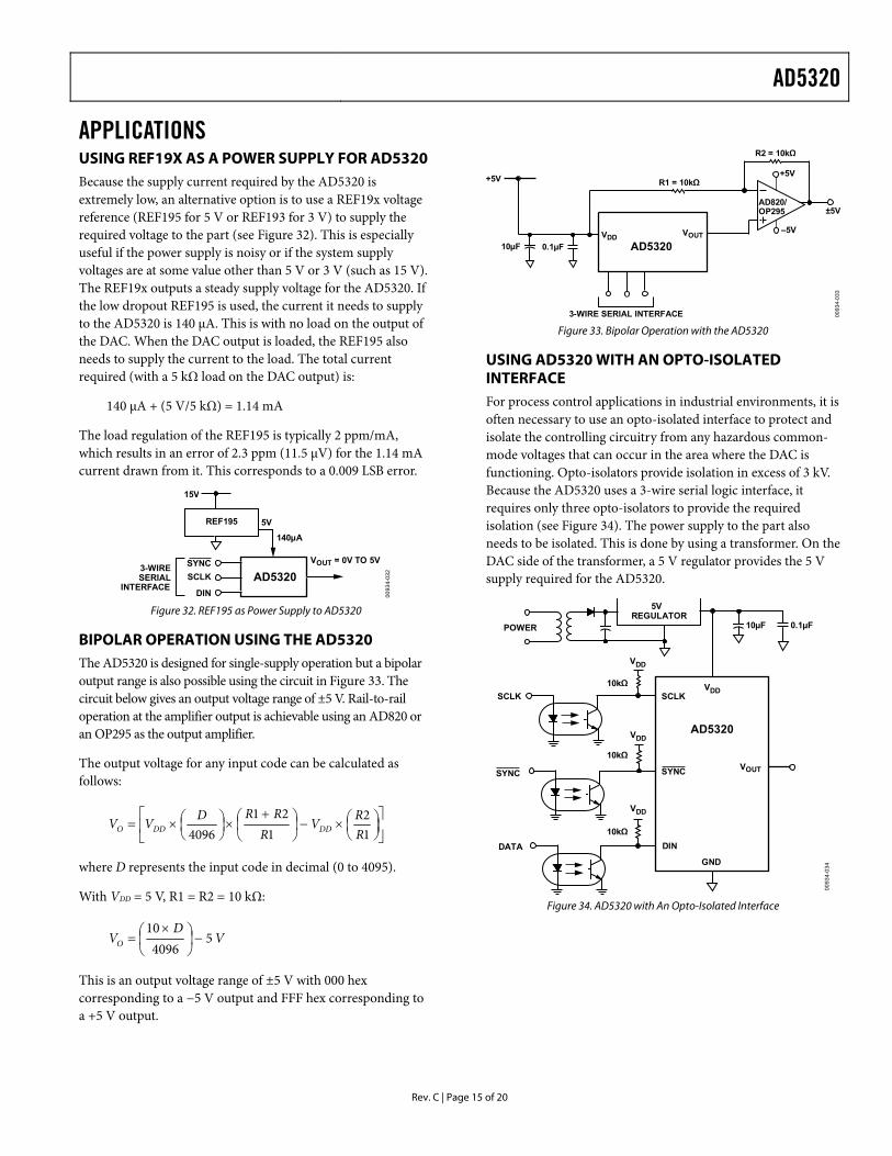
BIPOLAR OPERATION USING THE AD5320 The AD5320 is designed for single-supply operation but a bipolar output range is also possible using the circuit in Figure 33. The circuit below gives an output voltage range of ±5 V. Rail-to-rail operation at the amplifier output is achievable using an AD820 or an OP295 as the output amplifier.
The output voltage for any input code can be calculated as follows:
⎥⎦
⎤⎢⎣
⎡⎟⎠⎞
⎜⎝⎛×−⎟
⎠⎞
⎜⎝⎛ +
×⎟⎠⎞
⎜⎝⎛×=
12
121
4096 RRV
RRRDVV DDDDO
where D represents the input code in decimal (0 to 4095).
With VDD = 5 V, R1 = R2 = 10 kΩ:
VD
VO 54096
10−⎟
⎠⎞
⎜⎝⎛ ×
=
This is an output voltage range of ±5 V with 000 hex corresponding to a −5 V output and FFF hex corresponding to a +5 V output.
3-WIRE SERIAL INTERFACE
+5V
AD532010µF 0.1µFVDD VOUT
R1 = 10kΩ
R2 = 10kΩ
+5V
±5V
–5V
AD820/OP295
0093
4-03
3
Figure 33. Bipolar Operation with the AD5320
USING AD5320 WITH AN OPTO-ISOLATED INTERFACE For process control applications in industrial environments, it is often necessary to use an opto-isolated interface to protect and isolate the controlling circuitry from any hazardous common-mode voltages that can occur in the area where the DAC is functioning. Opto-isolators provide isolation in excess of 3 kV. Because the AD5320 uses a 3-wire serial logic interface, it requires only three opto-isolators to provide the required isolation (see Figure 34). The power supply to the part also needs to be isolated. This is done by using a transformer. On the DAC side of the transformer, a 5 V regulator provides the 5 V supply required for the AD5320.
VDD
0.1µF
VDD
10kΩ
10kΩ
VDD
10kΩ
5VREGULATOR
VOUT
GND
DIN
SYNC
SCLK
POWER 10µF
VDD
SYNC
SCLK
DATA
AD5320
0093
4-03
4
Figure 34. AD5320 with An Opto-Isolated Interface
AD5320
Rev. C | Page 16 of 20
POWER SUPPLY BYPASSING AND GROUNDING When accuracy is important in a circuit, it is helpful to consider carefully the power supply and ground return layout on the board. The printed circuit board containing the AD5320 should have separate analog and digital sections, each having its own area of the board. If the AD5320 is in a system where other devices require an AGND to DGND connection, the connec-tion should be made at one point only. This ground point should be as close as possible to the AD5320.
The power supply to the AD5320 should be bypassed with 10 μF capacitors and 0.1 μF capacitors. The capacitors should be physi-cally as close as possible to the device with the 0.1 μF capacitors ideally against the device. The 10 μF capacitors are the tantalum bead type. It is important that the 0.1 μF capacitors have low effective series resistance (ESR) and effective series inductance (ESI), such as common ceramic types of capacitors. The 0.1 μF capacitors provide a low impedance path to ground for high frequencies caused by transient currents due to internal logic switching.
The power supply line itself should have as large a trace as possible to provide a low impedance path and reduce glitch effects on the supply line. Clocks and other fast switching digital signals should be shielded from other parts of the board by digital ground. Avoid crossover of digital and analog signals if possible. When traces cross on opposite sides of the board, ensure that they run at right angles to each other to reduce feedthrough effects through the board. The best board layout technique is the microstrip technique where the component side of the board is dedicated to the ground plane only and the signal traces are placed on the solder side. However, this is not always possible with a two-layer board.
AD5320
Rev. C | Page 17 of 20
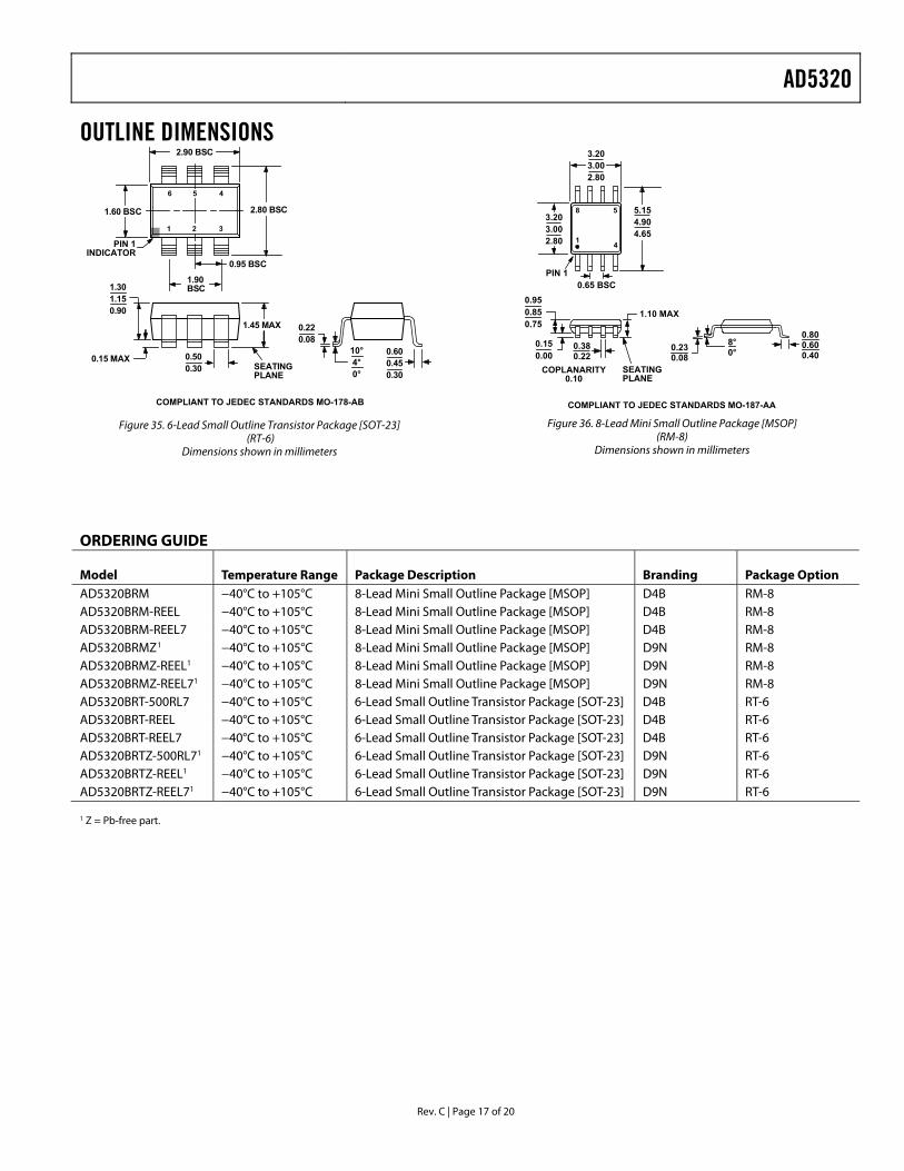
OUTLINE DIMENSIONS
1 3
45
2
6
2.90 BSC
1.60 BSC 2.80 BSC
1.90BSC
0.95 BSC
0.220.08
10°4°0°
0.500.30
0.15 MAX
1.301.150.90
SEATINGPLANE
1.45 MAX
0.600.450.30
PIN 1INDICATOR
COMPLIANT TO JEDEC STANDARDS MO-178-AB
Figure 35. 6-Lead Small Outline Transistor Package [SOT-23] (RT-6)
Dimensions shown in millimeters
COMPLIANT TO JEDEC STANDARDS MO-187-AA
0.800.600.40
8°0°
4
8
1
5
PIN 10.65 BSC
SEATINGPLANE
0.380.22
1.10 MAX
3.203.002.80
COPLANARITY0.10
0.230.08
3.203.002.80
5.154.904.65
0.150.00
0.950.850.75
Figure 36. 8-Lead Mini Small Outline Package [MSOP]
(RM-8) Dimensions shown in millimeters
ORDERING GUIDE Model
Temperature Range
Package Description
Branding
Package Option
AD5320BRM −40°C to +105°C 8-Lead Mini Small Outline Package [MSOP] D4B RM-8 AD5320BRM-REEL −40°C to +105°C 8-Lead Mini Small Outline Package [MSOP] D4B RM-8 AD5320BRM-REEL7 −40°C to +105°C 8-Lead Mini Small Outline Package [MSOP] D4B RM-8 AD5320BRMZ1 −40°C to +105°C 8-Lead Mini Small Outline Package [MSOP] D9N RM-8 AD5320BRMZ-REEL1 −40°C to +105°C 8-Lead Mini Small Outline Package [MSOP] D9N RM-8 AD5320BRMZ-REEL71 −40°C to +105°C 8-Lead Mini Small Outline Package [MSOP] D9N RM-8 AD5320BRT-500RL7 −40°C to +105°C 6-Lead Small Outline Transistor Package [SOT-23] D4B RT-6 AD5320BRT-REEL −40°C to +105°C 6-Lead Small Outline Transistor Package [SOT-23] D4B RT-6 AD5320BRT-REEL7 −40°C to +105°C 6-Lead Small Outline Transistor Package [SOT-23] D4B RT-6 AD5320BRTZ-500RL71 −40°C to +105°C 6-Lead Small Outline Transistor Package [SOT-23] D9N RT-6 AD5320BRTZ-REEL1 −40°C to +105°C 6-Lead Small Outline Transistor Package [SOT-23] D9N RT-6 AD5320BRTZ-REEL71 −40°C to +105°C 6-Lead Small Outline Transistor Package [SOT-23] D9N RT-6 1 Z = Pb-free part.

AD5320
Rev. C | Page 18 of 20
NOTES

AD5320
Rev. C | Page 19 of 20
NOTES

AD5320
Rev. C | Page 20 of 20
NOTES
© 2005 Analog Devices, Inc. All rights reserved. Trademarks and registered trademarks are the property of their respective owners. D00934-0-11/05(C)

![Very Low Noise, 24-Bit Analog-to-Digital Converter datasheet ...SDCS[1:0] = 01 0.5 μA Sensor detect current sources SDCS[1:0] = 10 2 μA SDCS[1:0] = 11 10 μA System Performance Resolution](https://img.pdfslide.us/doc/110x75/6100382d24f9d517681b0bc7/very-low-noise-24-bit-analog-to-digital-converter-datasheet-sdcs10-01.jpg)