Embed Size (px)
Citation preview
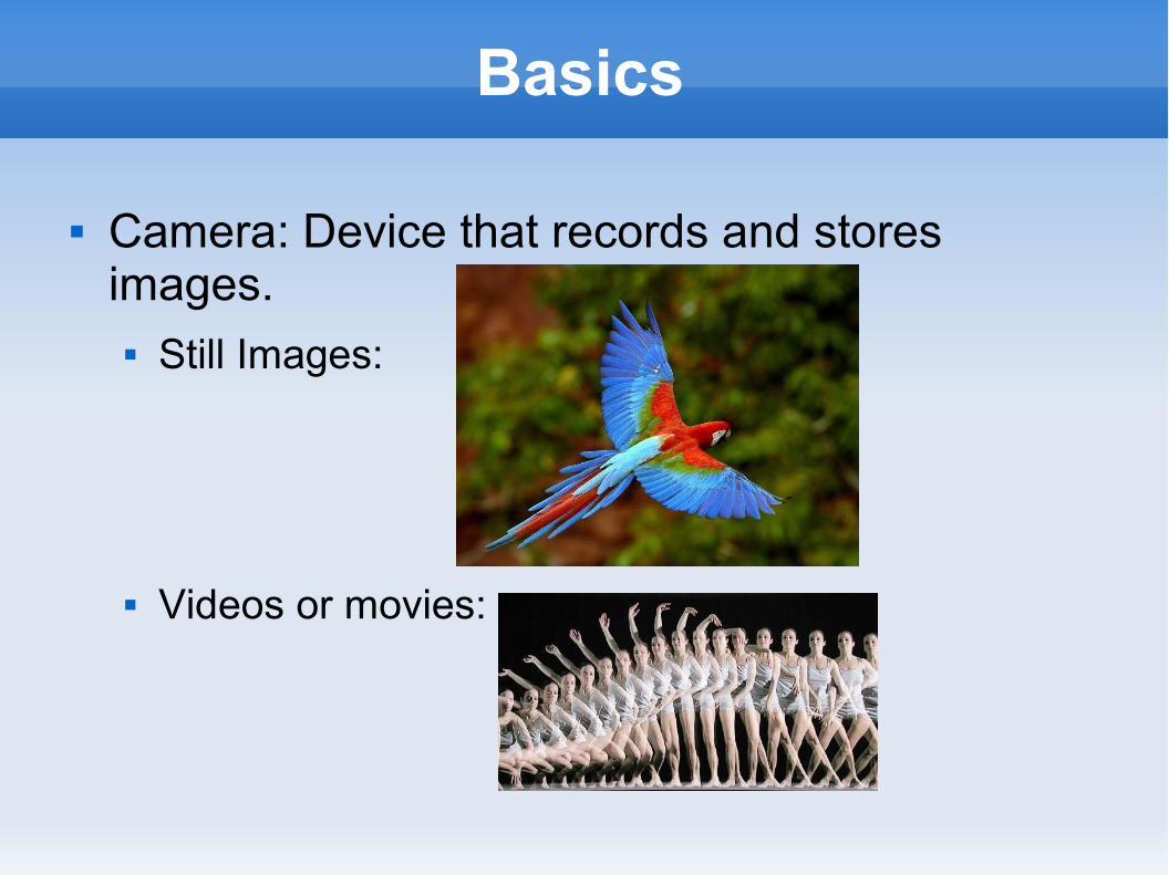
Basics
Camera: Device that records and stores images.
Still Images:
Videos or movies:
Basics
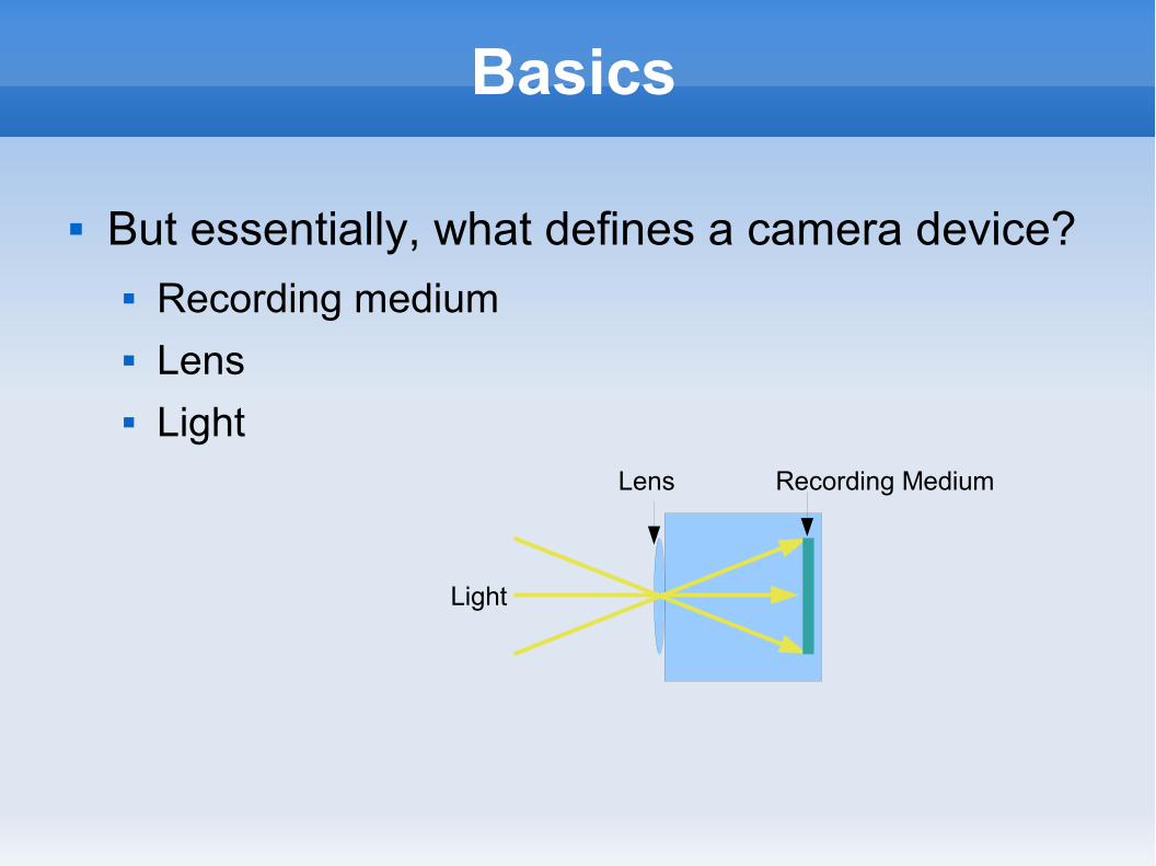
But essentially, what defines a camera device? Recording medium Lens Light
Light
Lens Recording Medium
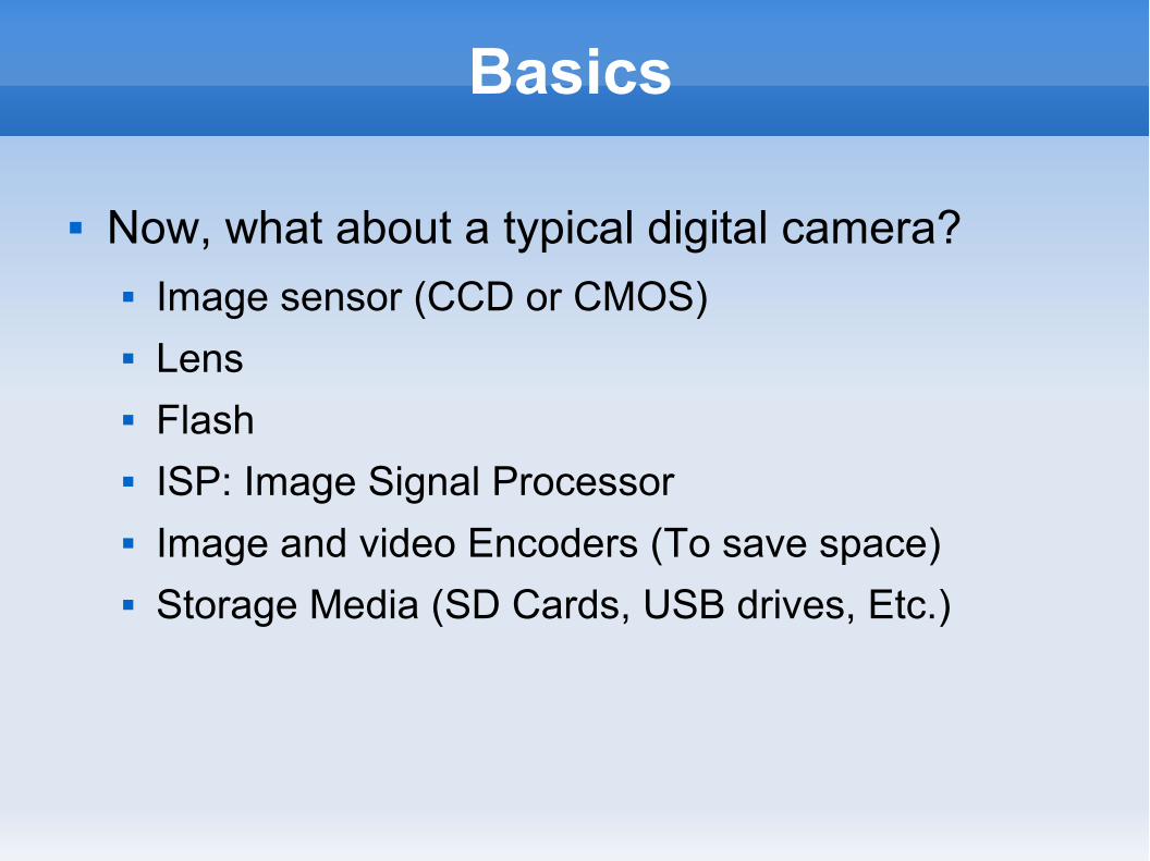
Basics
Now, what about a typical digital camera? Image sensor (CCD or CMOS) Lens Flash ISP: Image Signal Processor Image and video Encoders (To save space) Storage Media (SD Cards, USB drives, Etc.)
Image sensors
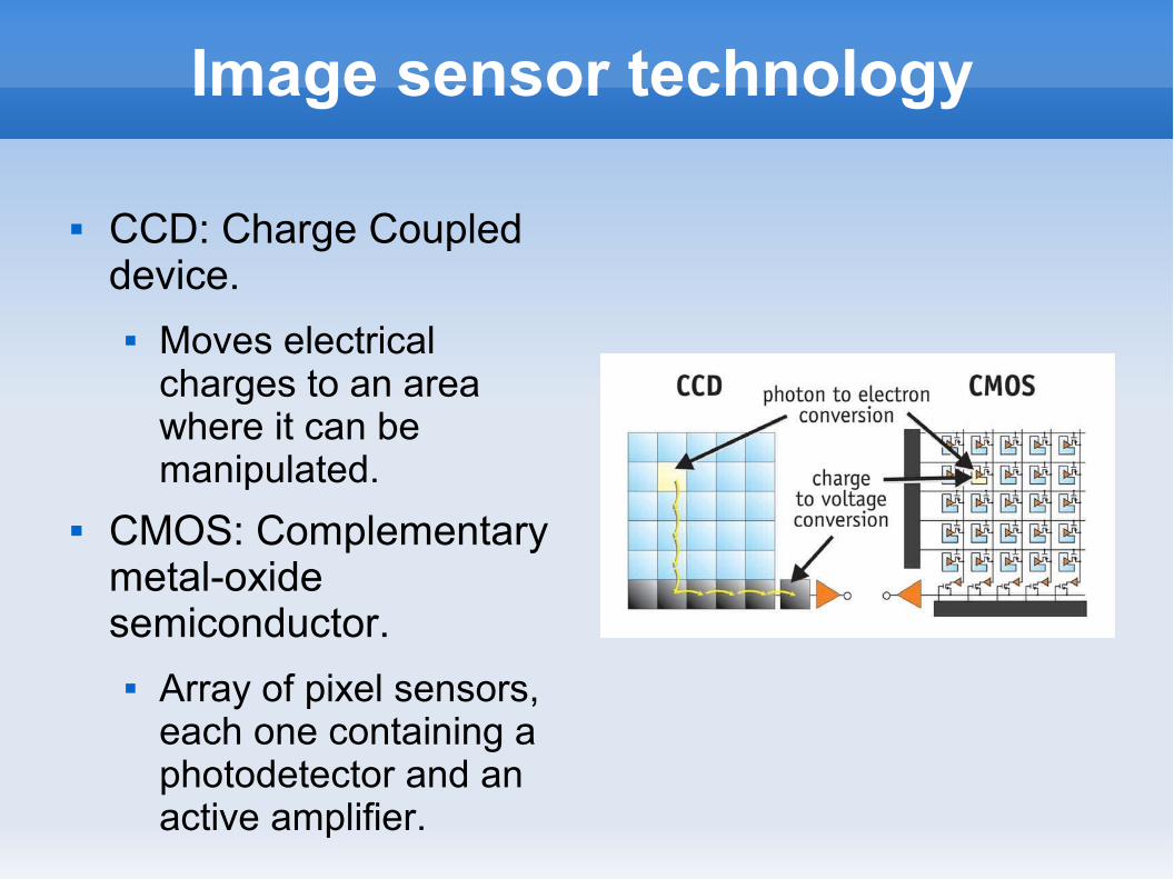
Image sensor technology
CCD: Charge Coupled device.
Moves electrical charges to an area where it can be manipulated.
CMOS: Complementary metal-oxide semiconductor.
Array of pixel sensors, each one containing a photodetector and an active amplifier.
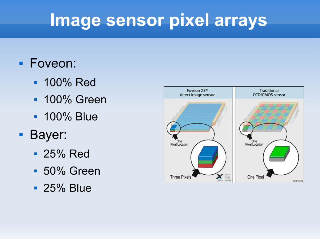
Image sensor pixel arrays
Foveon: 100% Red 100% Green 100% Blue
Bayer: 25% Red 50% Green 25% Blue

Image sensor formats(Most typical)
RAW 10-bits. 10-bit digital value obtained thru an ADC (Analog to
Digital Converter) of the analog voltage coming from each pixel's associated photodetector charge-to-voltage converter.
YUV 4:2:2 8-bits. Represent pairs of horizontally contiguous pixels. 8-
bits per component (Y: Luminance, UV: Chrominance). Order is usually YUYV, or UYVY. Croma components (UV) are subsampled at half the sample rate than luma (Y).
Image sensor formats(Most typical)
YUV 4:2:0 8-bits. Similar to 4:2:2, but the difference being that the UV
components are also vertically subsampled by 2. This format contains interleaved data, which means, odd lines contain only Y elements, and even lines contain packed UYVY elements, similarly to 4:2:2 subsampling.
NV12 (YUV 4:2:0 8-bits, planar) Exact same subsampling as above format, but the
difference being that one array contains only Y components, and a second array contains packed UV components, 2x2 subsampled.
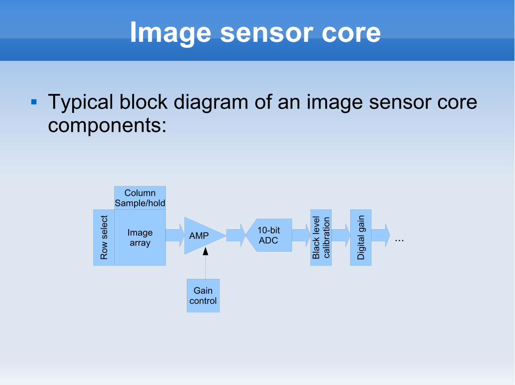
Image sensor core
Typical block diagram of an image sensor core components:
Imagearray
Row
sel
ect
ColumnSample/hold
AMP10-bitADC
Bla
ck le
vel
calib
ratio
n
Dig
ital g
ain
...
Gaincontrol
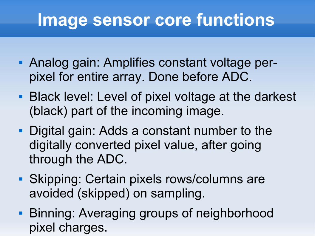
Image sensor core functions
Analog gain: Amplifies constant voltage per-pixel for entire array. Done before ADC.
Black level: Level of pixel voltage at the darkest (black) part of the incoming image.
Digital gain: Adds a constant number to the digitally converted pixel value, after going through the ADC.
Skipping: Certain pixels rows/columns are avoided (skipped) on sampling.
Binning: Averaging groups of neighborhood pixel charges.
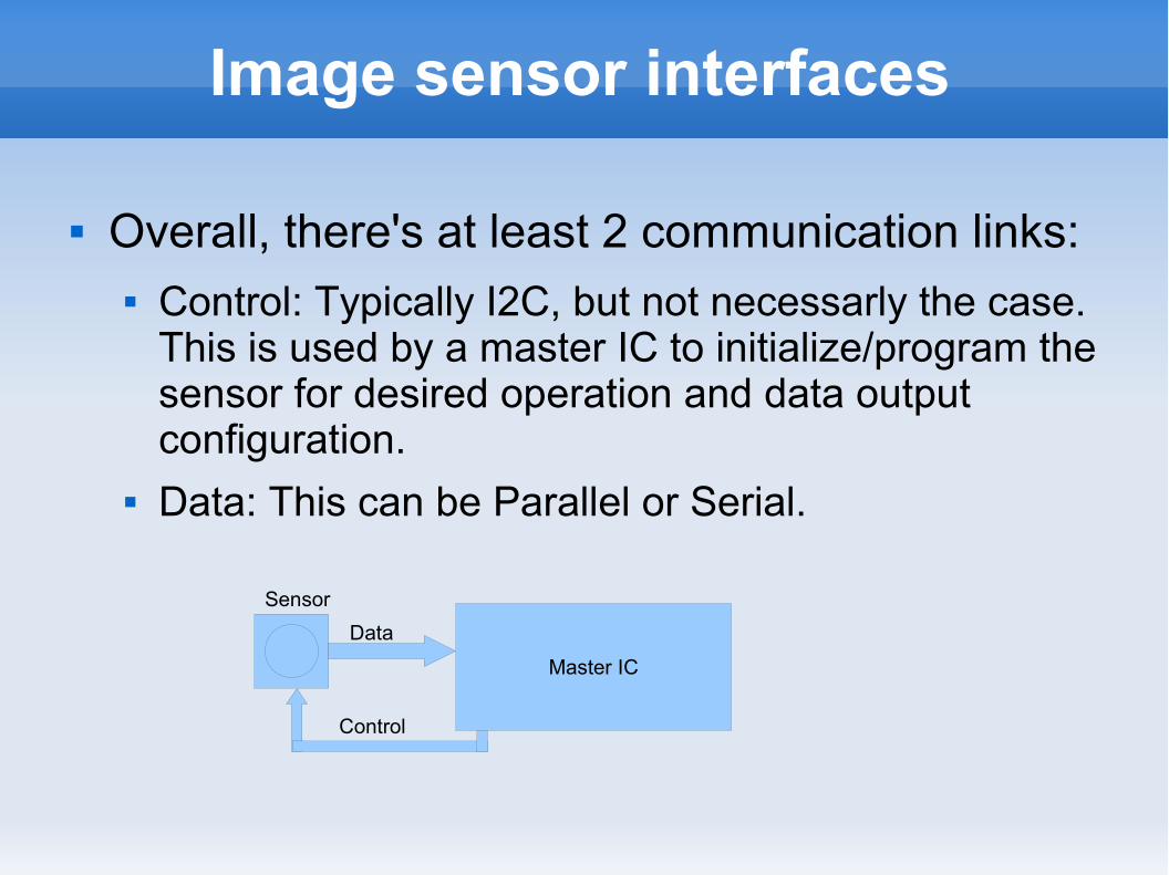
Image sensor interfaces
Overall, there's at least 2 communication links: Control: Typically I2C, but not necessarly the case.
This is used by a master IC to initialize/program the sensor for desired operation and data output configuration.
Data: This can be Parallel or Serial.
Master IC
Sensor
Data
Control

Image sensor interfaces - Control
I2C: Inter-Integrated Circuit Multi-master serial single-ended computer bus,
used to attach low-speed peripherals to a host IC. Uses 2 open-drain lines, w/pull-up resistors:
SCL (Serial CLock). SDA (Serial DAta).

Image sensor interfaces - I2C
I2C: Inter-Integrated Circuit START and STOP conditions to claim/release bus control.
First byte: 7-bit device address space, 1 bit used to indicate Read (HI) or Write (LOW).
ACK bit pulled low by slave after each byte sent, used to handshake transmission between master and slave ICs. If ACK bit is high, master should stop transmission.

Image sensor interfaces - Parallel
Parallel interface (a.k.a. Digital Video Port) Data signals: 1 digital output pin per bit. Sync signals:
PCLK: Pixel Clock. HSYNC: Horizontal Sync. VSYNC: Vertical Sync.
Sensor Master IC
D[9:0]
PCLK
HSYNC
VSYNC
Image data
Hor
izon
tal B
lan
kin
g
Vertical Blanking

Image sensor interfaces - CSI2
MIPI CSI2 (Camera Serial Interface 2). Data signals: Up to 4 differential lanes (+/- signals). Clock signals: 1 differential lane (+/- signals).
Speeds up to 1 Gbit/s per lane (500 MHz)
Sensor Master IC
CLK (+/-)
DAT0 (+/-)
DAT1 (+/-)
DAT2 (+/-)
DAT3 (+/-)

Image sensor interfaces - CSI2
CSI2 Receiver components:

Image sensor interfaces - CSI2
D-PHY layer:
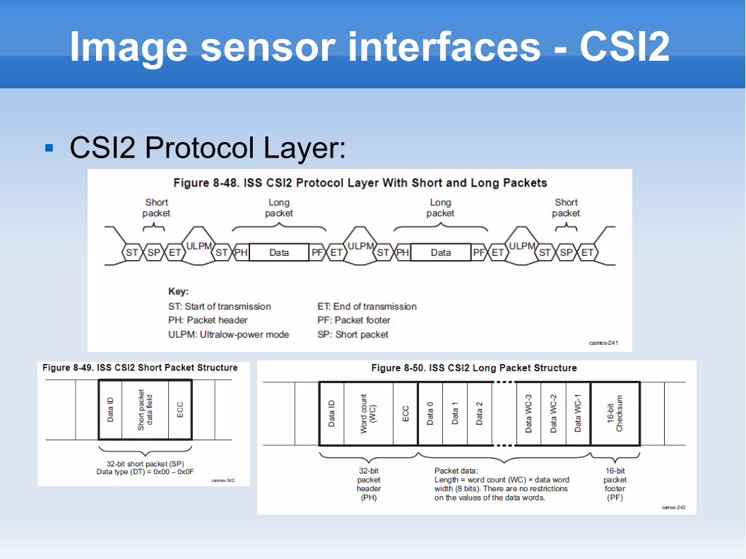
Image sensor interfaces - CSI2
CSI2 Protocol Layer:
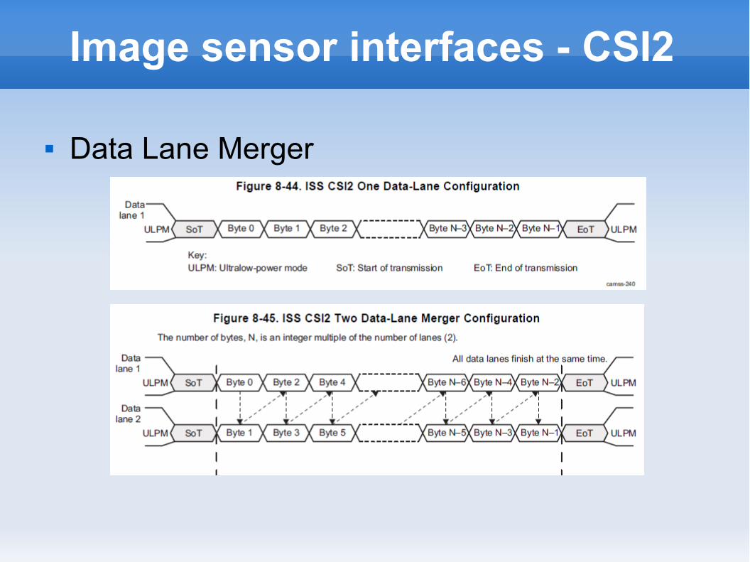
Image sensor interfaces - CSI2
Data Lane Merger
Lens
Lens
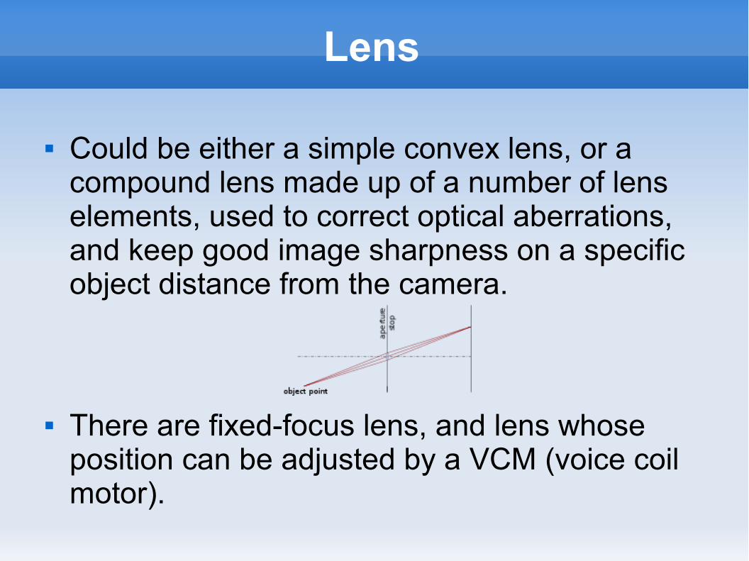
Could be either a simple convex lens, or a compound lens made up of a number of lens elements, used to correct optical aberrations, and keep good image sharpness on a specific object distance from the camera.
There are fixed-focus lens, and lens whose position can be adjusted by a VCM (voice coil motor).
Lens
For moving lens, position can be either controlled as part of the image sensor registers, or as a separate I2C device in the bus.
This is usually done as a result of the Auto Focus algorithm, after analyzing the captured images. It can also be due to manual control, if desired.
Flash
Flash
Used in photography to compensate natural ambient light, and illuminate a dark scene.
Syncronized with start of capture image command, with adjusted flashing duration, and intensity.
Usually triggered with GPIOs and configured with I2C commands.

Thanks!

Extra slides

Image sensor interfaces - Data
MIPI CSI (Camera Serial Interface). Data signals: 1 differential lane (+/- signals). Clock signals: 1 differential lane (+/- signals).
Speeds between 1->208 Mbps
Sensor Master IC
CLK (+/-)
DAT (+/-)
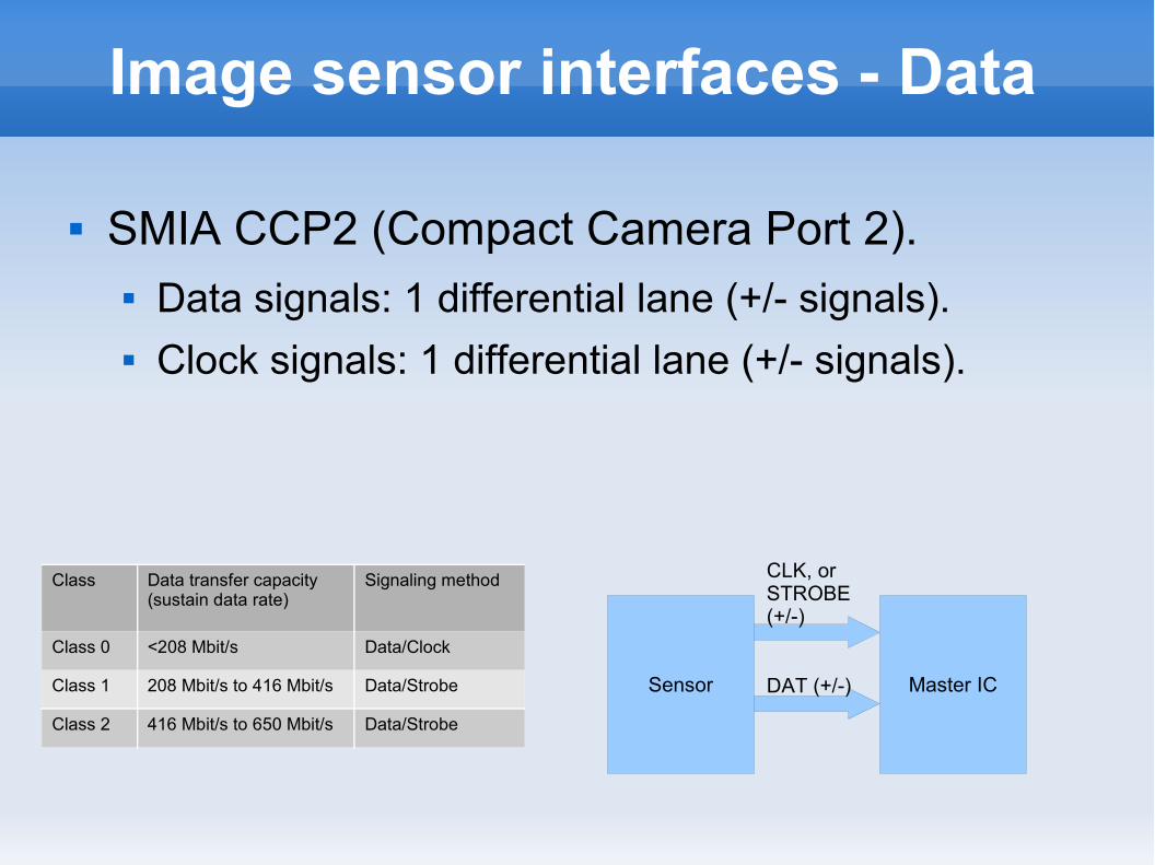
Image sensor interfaces - Data
SMIA CCP2 (Compact Camera Port 2). Data signals: 1 differential lane (+/- signals). Clock signals: 1 differential lane (+/- signals).
Sensor Master IC
CLK, orSTROBE(+/-)
DAT (+/-)
Class Data transfer capacity(sustain data rate)
Signaling method
Class 0 <208 Mbit/s Data/Clock
Class 1 208 Mbit/s to 416 Mbit/s Data/Strobe
Class 2 416 Mbit/s to 650 Mbit/s Data/Strobe


![Marketresearchcoverpage 110614005815-phpapp02[2]](https://img.pdfslide.us/doc/110x75/546cc99daf795980298b5105/marketresearchcoverpage-110614005815-phpapp022.jpg)


![Benefitsofusingtechnologyintheclassroom 100702182855-phpapp02[2]](https://img.pdfslide.us/doc/110x75/547560e4b4af9fc30a8b5a27/benefitsofusingtechnologyintheclassroom-100702182855-phpapp022.jpg)

![Rollingofmetals 110104143819 Phpapp02[2]](https://img.pdfslide.us/doc/110x75/55cf852e550346484b8b8aa1/rollingofmetals-110104143819-phpapp022.jpg)