Embed Size (px)
Citation preview
XR76115
15A Synchronous Step Down COT Regulator
www.maxlinear.com Rev 1D
General Description
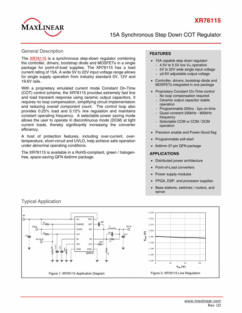
The XR76115 is a synchronous step-down regulator combining the controller, drivers, bootstrap diode and MOSFETs in a single package for point-of-load supplies. The XR76115 has a load current rating of 15A. A wide 5V to 22V input voltage range allows for single supply operation from industry standard 5V, 12V and 19.6V rails.
With a proprietary emulated current mode Constant On-Time (COT) control scheme, the XR76115 provides extremely fast line and load transient response using ceramic output capacitors. It requires no loop compensation, simplifying circuit implementation and reducing overall component count. The control loop also provides 0.25% load and 0.12% line regulation and maintains constant operating frequency. A selectable power saving mode allows the user to operate in discontinuous mode (DCM) at light current loads, thereby significantly increasing the converter efficiency.
A host of protection features, including over-current, over-temperature, short-circuit and UVLO, help achieve safe operation under abnormal operating conditions.
The XR76115 is available in a RoHS-compliant, green / halogen-free, space-saving QFN 6x6mm package.
FEATURES • 15A capable step down regulator
− 4.5V to 5.5V low VIN operation − 5V to 22V wide single input voltage − ≥0.6V adjustable output voltage
• Controller, drivers, bootstrap diode and MOSFETs integrated in one package
• Proprietary Constant On-Time control − No loop compensation required − Ceramic output capacitor stable
operation − Programmable 200ns - 2µs on-time − Quasi constant 200kHz - 800kHz
frequency − Selectable CCM or CCM / DCM
operation
• Precision enable and Power-Good flag
• Programmable soft-start
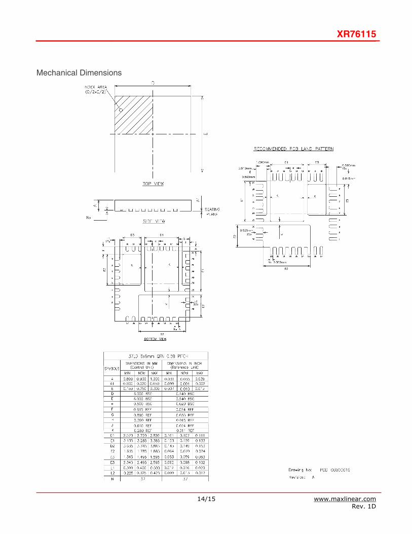
• 6x6mm 37-pin QFN package
APPLICATIONS
• Distributed power architecture
• Point-of-Load converters
• Power supply modules
• FPGA, DSP, and processor supplies
• Base stations, switches / routers, and server
Typical Application
Figure 1: XR76115 Application Diagram Figure 2: XR76115 Line Regulation
1.180
1.185
1.190
1.195
1.200
1.205
1.210
1.215
1.220
5 10 15 20
VO
UT
(V)
VIN (V)
XR76115
2/15 www.maxlinear.com Rev. 1D
Absolute Maximum Ratings These are stress ratings only and functional operation of the device at these ratings or any other above those indicated in the operation sections of the specifications below is not implied. Stresses beyond those listed under Absolute Maximum Ratings may cause permanent damage to the device. Exposure to any Absolute Maximum Rating condition for extended periods may affect device reliability and lifetime.
PVIN, VIN ...................................................................... -0.3V to 25V VCC ............................................................................. -0.3V to 6.0V BST .......................................................................... -0.3V to 31V(1) BST-SW ........................................................................ -0.3V to 6V SW, ILIM ..................................................................... -1V to 25V(1,2) All other pins ....................................................... -0.3V to VCC+0.3V Storage temperature ................................................ -65°C to 150°C Junction temperature ............................................................. 150°C Power dissipation ................................................. Internally Limited Lead temperature (soldering, 10 sec) .................................... 300°C ESD rating (HBM - Human Body Model) ................................... 2kV
Operating Ratings PVIN ................................................................................. 3V to 22V VIN ................................................................................ 4.5V to 22V VCC .............................................................................. 4.5V to 5.5V SW, ILIM ....................................................................... -1V to 22V(2) PGOOD, VCC, TON, SS, EN .......................................... -0.3V to 5.5V Switching Frequency ......................................... 200kHz - 800kHz(3) Junction Temperature Range (TJ) ............................ -40°C to 125°C XR76115 Package Power Dissipation max at 25°C ................ 5.2W XR76115 JEDEC51 Package Thermal Resistance θJA ........ 19°C/W
Note 1: No external voltage applied Note 2: SW pin’s DC range is -1V, transient is -5V for less than 50ns Note 3: Recommended
Ordering Information(1)
Part Number Operating Temperature Range Package Packing Method Lead-Free(2)
XR76115EL-F -40°C≤TJ≤+125°C 6x6mm QFN Bulk Yes
XR76115ELTR-F -40°C≤TJ≤+125°C 6x6mm QFN Tape & Reel Yes
XR76115EVB XR76115 Evaluation Board
NOTES:
1. Refer to www.maxlinear.com/XR76115 for most up-to-date Ordering Information.
2. Visit www.maxlinear.com for additional information on Environmental Rating.
Electrical Characteristics Specifications are for the operating junction temperature of TJ = 25°C only; limits applying over the full operating junction temperature range are denoted by a “•”. Typical values represent the most likely parametric norm at TJ = 25°C, and are provided for reference purposes only. Unless otherwise indicated, VIN=12V.
Parameter Min. Typ. Max. Units Conditions
Power Supply Characteristics
VIN, input voltage range 5 12 22
V • VCC regulating
4.5 5.0 5.5 VCC tied to VIN
IVIN, VIN supply current 0.7 1.3 mA • Not switching, VIN = 12V, VFB = 0.7V
IVCC, VCC quiescent current 0.7 1.3 mA • Not switching, VCC = VIN = 5V, VFB = 0.7V
IVIN, VIN supply current 11 mA f = 300kHz, RON = 107k, VFB = 0.58V
IOFF, shutdown current 0.5 μA Enable = 0V, VIN = 12V, VIN = PVIN
Enable and Under-Voltage Lock-Out UVLO VIH_EN, EN pin rising threshold 1.8 1.9 2.0 V •
VEN_HYS, EN pin hysteresis 50 mV
VIH_EN, EN pin rising threshold for DCM / CCM operation 2.8 3.0 3.1 V •
VEN_HYS, EN pin hysteresis 100 mV
VCC UVLO start threshold, rising edge 4.00 4.25 4.50 V •
VCC UVLO hysteresis 200 mV
XR76115
3/15 www.maxlinear.com Rev. 1D
Parameter Min. Typ. Max. Units Conditions
Reference Voltage
VREF, reference voltage
0.597 0.600 0.603 V VIN = 5V - 22V VCC regulating
0.596 0.600 0.604 V VIN = 4.5V - 5.5V VCC tied to VIN
0.594 0.600 0.606 V • VIN = 5V - 22V VCC regulating, VIN = 4.5V - 5.5V VCC tied to VIN
DC load regulation ±0.25 % CCM operation, closed loop, applies to any COUT DC line regulation ±0.12 %
Programmable Constant On-Time On-time 1 1.66 1.95 2.24 µs • RON = 140kΩ, VIN = 22V
f corresponding to on-time 1 243 280 329 kHz VIN = 22V, VOUT = 12V
Minimum programmable on-time 109 ns RON = 6.98kΩ, VIN = 22V
On-time 2 170 200 230 ns • RON = 6.98kΩ, VIN = 12V
f corresponding to on-time 2 362 417 490 kHz VOUT = 1.0V
On-time 3 365 430 495 ns • RON = 16.2kΩ, VIN = 12V
Minimum off-time 250 350 ns •
Diode Emulation Mode Zero crossing threshold -2 mV DC value measured during test
Soft-Start SS charge current -14 -10 -6 µA •
SS discharge current 1 3 mA • Fault present
VCC Linear Regulator
VCC output voltage 4.8 5.0 5.2
V • VIN = 6V to 22V, Iload = 0 to 30mA
4.51 4.7 • VIN = 5V, Iload = 0 to 20mA
Dropout voltage 100 300 490 mV • IVCC = 30mA
Power Good Output Power Good threshold -10 -7.5 -5 %
Power Good hysteresis 2 4 %
Power Good sink current 1 15 mA
Protection: OCP, OTP, Short-Circuit Hiccup timeout 110 ms
ILIM pin source current 45 50 55 µA
ILIM current temperature coefficient 0.4 %/°C
ILIM comparator offset -8 0 +8 mV •
Current limit blanking 100 ns
Thermal shutdown threshold 150 °C Rising temperature
Thermal hysteresis 15 °C
Feedback pin short-circuit threshold 50 60 70 % • Percent of VREF, short circuit is active After PGOOD is up
Output Power Stage High-side MOSFET RDSON 7 10 mΩ VGS = 4.5V, IDS = 2A
Low-side MOSFET RDSON 4 4.6 mΩ VGS = 4.5V, IDS = 2A
Maximum output current 15 A •
XR76115
4/15 www.maxlinear.com Rev. 1D
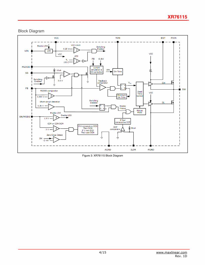
Block Diagram
Figure 3: XR76115 Block Diagram
XR76115
5/15 www.maxlinear.com Rev. 1D
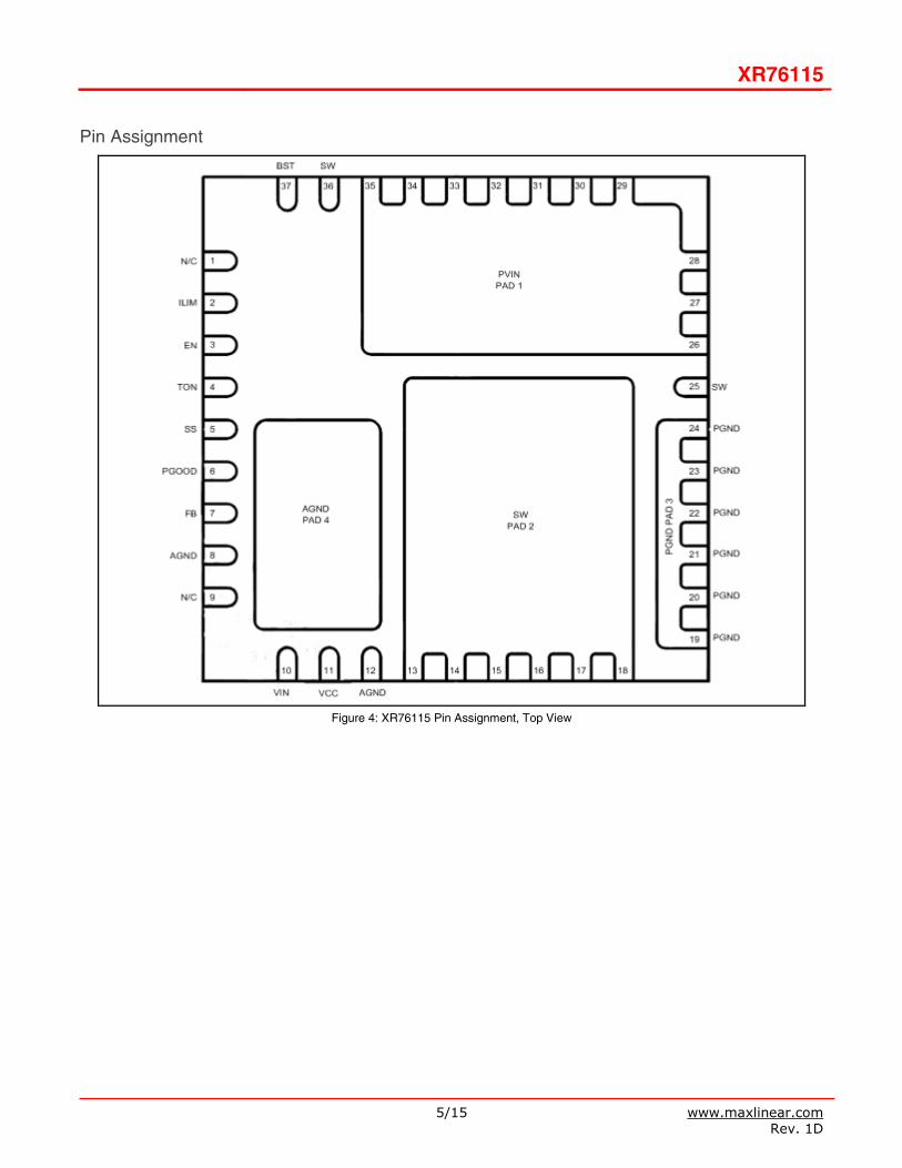
Pin Assignment
Figure 4: XR76115 Pin Assignment, Top View
XR76115
6/15 www.maxlinear.com Rev. 1D
Pin Description
Name Pin Number Description
NC 1,9 Not connected.
ILIM 2 Over-current protection programming. Connect with a resistor to SW.
EN/MODE 3 Precision enable pin. Pulling this pin above 1.9V will turn the regulator on and it will operate in CCM. If the voltage is raised above 3.0V then the regulator will operate in DCM / CCM depending on load.
TON 4 Constant on-time programming pin. Connect with a resistor to AGND.
SS 5 Soft-start pin. Connect an external capacitor between SS and AGND to program the soft-start rate based on the 10µA internal source current.
PGOOD 6 Power-good output. This open-drain output is pulled low when VOUT is outside the regulation.
FB 7 Feedback input to feedback comparator. Connect with a set of resistors to VOUT and AGND in order to program VOUT.
AGND 8, 12,
AGND Pad Signal ground for control circuitry. Connect AGND Pad with a short trace to pins 8 and 12.
VIN 10 Supply input for the regulator’s LDO. Normally it is connected to PVIN.
VCC 11 The output of regulator’s LDO. For operation using a 5V rail, VCC should be shorted to VIN.
SW 13-18, 25, 36, SW
Pad Switch node. The drain of the low-side N-channel MOSFET. The source of the high-side MOSFET is wire-bonded to the SW pad.
PGND 19-24,
PGND Pad Ground of the power stage. Should be connected to the system’s power ground plane. The source of the low-side MOSFET is wire-bonded to PGND Pad.
PVIN 26-35,
PVIN Pad Input voltage for the power stage. The drain of the high-side N-channel MOSFET.
BST 37 High-side driver supply pin. Connect a 1µF bootstrap capacitor between BST and SW.
XR76115
7/15 www.maxlinear.com Rev. 1D
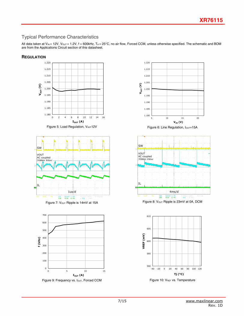
Typical Performance Characteristics All data taken at VIN = 12V, VOUT = 1.2V, f = 600kHz, TA = 25°C, no air flow, Forced CCM, unless otherwise specified. The schematic and BOM are from the Applications Circuit section of this datasheet.
REGULATION
Figure 5: Load Regulation, VIN=12V
Figure 6: Line Regulation, IOUT=15A
Figure 7: VOUT Ripple is 14mV at 15A
Figure 8: VOUT Ripple is 23mV at 0A, DCM
Figure 9: Frequency vs. IOUT, Forced CCM
Figure 10: VREF vs. Temperature
1.180
1.185
1.190
1.195
1.200
1.205
1.210
1.215
1.220
0 2 4 6 8 10 12 14 16
VO
UT
(V)
IOUT (A)
1.180
1.185
1.190
1.195
1.200
1.205
1.210
1.215
1.220
5 10 15 20
VO
UT
(V)
VIN (V)
0
100
200
300
400
500
600
700
0 5 10 15
f (k
Hz)
IOUT (A)
590
595
600
605
610
-40 -20 0 20 40 60 80 100 120
VR
EF (
mV
)
Tj (°C)
1us/d
SW
VOUT AC coupled 20MHz Filter
IL
4ms/d
IL
SW
VOUT AC coupled 20MHz Filter
XR76115
8/15 www.maxlinear.com Rev. 1D
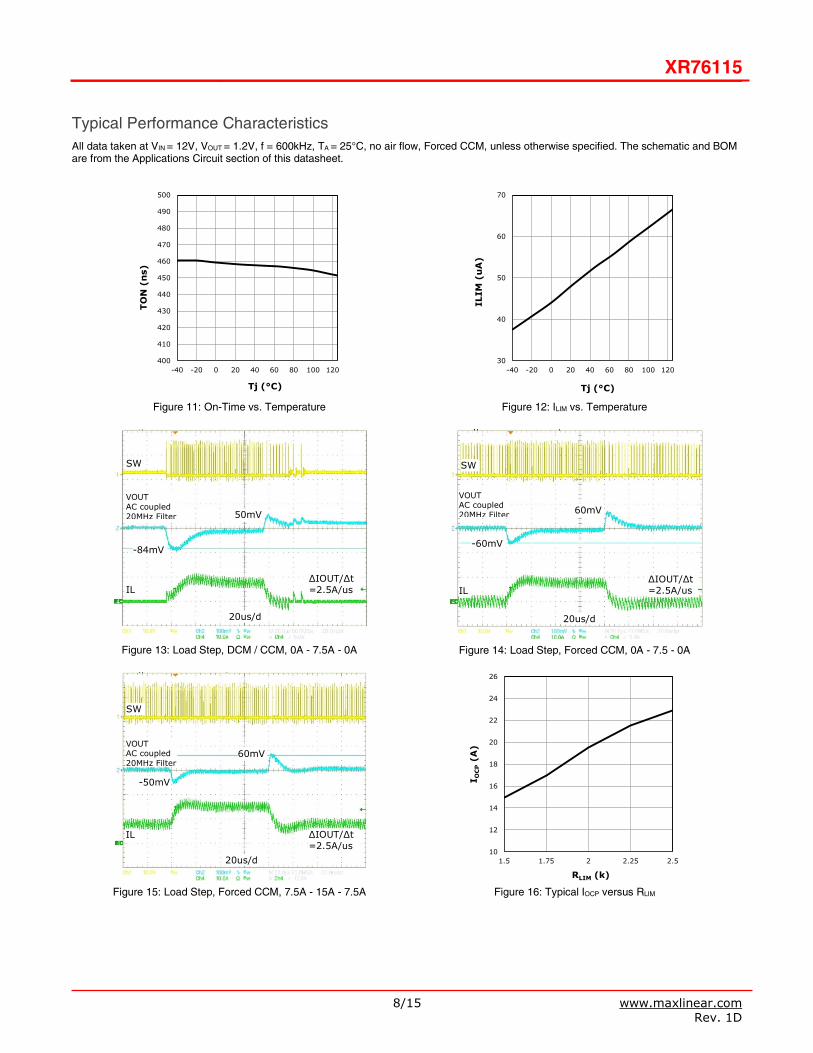
Typical Performance Characteristics All data taken at VIN = 12V, VOUT = 1.2V, f = 600kHz, TA = 25°C, no air flow, Forced CCM, unless otherwise specified. The schematic and BOM are from the Applications Circuit section of this datasheet.
Figure 11: On-Time vs. Temperature
Figure 12: ILIM vs. Temperature
Figure 13: Load Step, DCM / CCM, 0A - 7.5A - 0A
Figure 14: Load Step, Forced CCM, 0A - 7.5 - 0A
Figure 15: Load Step, Forced CCM, 7.5A - 15A - 7.5A
Figure 16: Typical IOCP versus RLIM
400
410
420
430
440
450
460
470
480
490
500
-40 -20 0 20 40 60 80 100 120
TON
(n
s)
Tj (°C)
30
40
50
60
70
-40 -20 0 20 40 60 80 100 120
ILIM
(u
A)
Tj (°C)
10
12
14
16
18
20
22
24
26
1.5 1.75 2 2.25 2.5
I OC
P(A
)
RLIM (k)
SW SW
20us/d 20us/d
VOUT AC coupled 20MHz Filter
VOUT AC coupled 20MHz Filter
IL IL ∆IOUT/∆t=2.5A/us
∆IOUT/∆t=2.5A/us
-84mV
50mV 60mV
-60mV
SW
VOUT AC coupled 20MHz Filter
IL
20us/d
-50mV
60mV
∆IOUT/∆t=2.5A/us
XR76115
9/15 www.maxlinear.com Rev. 1D
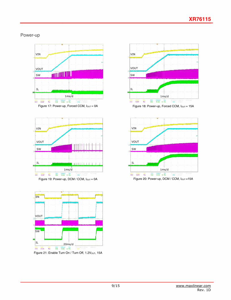
Power-up
Figure 17: Power-up, Forced CCM, IOUT = 0A
Figure 18: Power-up, Forced CCM, IOUT = 15A
Figure 19: Power-up, DCM / CCM, IOUT = 0A
Figure 20: Power-up, DCM / CCM, IOUT =15A
Figure 21: Enable Turn On / Turn Off, 1.2VOUT, 15A
SW SW
SW SW
IL
IL IL
IL
VIN VIN
VIN VIN
VOUT
VOUT
VOUT
VOUT
1ms/d 1ms/d
1ms/d 1ms/d
IL
SW
VOUT
EN
20ms/d
XR76115
10/15 www.maxlinear.com Rev. 1D
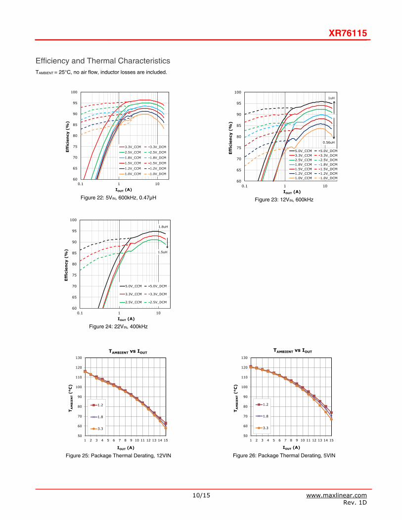
Efficiency and Thermal Characteristics TAMBIENT = 25°C, no air flow, inductor losses are included.
Figure 22: 5VIN, 600kHz, 0.47µH
Figure 23: 12VIN, 600kHz
Figure 24: 22VIN, 400kHz
Figure 25: Package Thermal Derating, 12VIN
Figure 26: Package Thermal Derating, 5VIN
60
65
70
75
80
85
90
95
100
0.1 1 10
Effi
cien
cy (
%)
IOUT (A)
3.3V_CCM 3.3V_DCM
2.5V_CCM 2.5V_DCM
1.8V_CCM 1.8V_DCM
1.5V_CCM 1.5V_DCM
1.2V_CCM 1.2V_DCM
1.0V_CCM 1.0V_DCM
60
65
70
75
80
85
90
95
100
0.1 1 10
Effi
cien
cy (
%)
IOUT (A)
5.0V_CCM 5.0V_DCM3.3V_CCM 3.3V_DCM2.5V_CCM 2.5V_DCM1.8V_CCM 1.8V_DCM1.5V_CCM 1.5V_DCM1.2V_CCM 1.2V_DCM1.0V_CCM 1.0V_DCM
1uH
0.56uH
60
65
70
75
80
85
90
95
100
0.1 1 10
Effi
cien
cy (
%)
IOUT (A)
5.0V_CCM 5.0V_DCM
3.3V_CCM 3.3V_DCM
2.5V_CCM 2.5V_DCM
1.5uH
1.8uH
50
60
70
80
90
100
110
120
130
1 2 3 4 5 6 7 8 9 10 11 12 13 14 15
T AM
BIE
NT
(°C
)
IOUT (A)
TAMBIENT vs IOUT
1.2
1.8
3.3
50
60
70
80
90
100
110
120
130
1 2 3 4 5 6 7 8 9 10 11 12 13 14 15
T AM
BIE
NT
(°C
)
IOUT (A)
TAMBIENT vs IOUT
1.2
1.8
3.3
XR76115
11/15 www.maxlinear.com Rev. 1D
Detailed Operation The XR76115 uses a synchronous step-down, proprietary emulated current-mode Constant On-Time (COT) control scheme. The on-time, which is programmed via RON, is inversely proportional to VIN and maintains a nearly constant frequency. The emulated current-mode control allows the use of ceramic output capacitors.
Each switching cycle begins with the high-side (switching) FET turning on for a pre-programmed time. At the end of the on-time, the high-side FET is turned off and the low-side (synchronous) FET is turned on for a preset minimum time (250ns nominal). This parameter is termed the Minimum Off-Time. After the Minimum Off-Time, the voltage at the feedback pin FB is compared to an internal voltage ramp at the feedback comparator. When VFB drops below the ramp voltage, the high-side FET is turned on and the cycle repeats. This voltage ramp constitutes an emulated current ramp and allows for the use of ceramic capacitors, in addition to other capacitor types, for output filtering.
Enable / Mode The EN/MODE pin accepts a tri-level signal that is used to control channel turn-on and turn-off. It also selects between two modes of operation: ‘Forced CCM’ and ‘DCM / CCM’. If EN is pulled below 1.9V, the regulator shuts down. A voltage between 1.9V and 3V selects the Forced CCM mode, which will run the converter in continuous conduction for all load currents. A voltage higher than 3V selects the DCM / CCM mode, which will run the converter in discontinuous conduction mode at light loads.
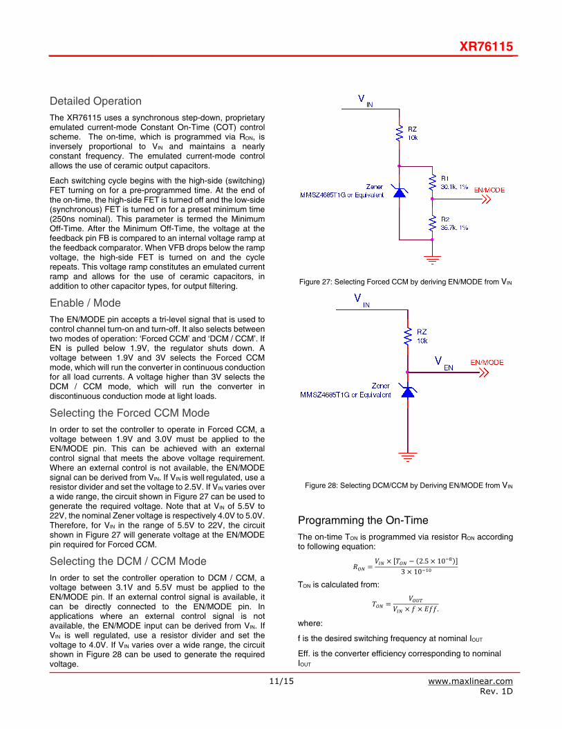
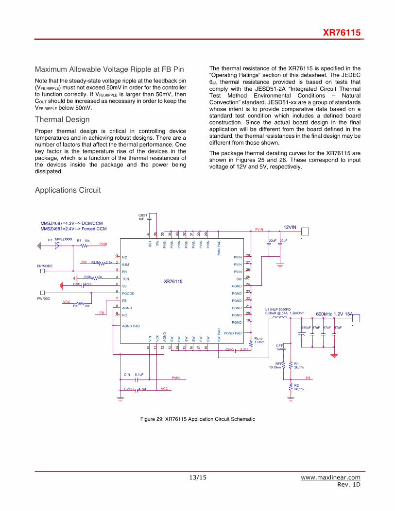
Selecting the Forced CCM Mode In order to set the controller to operate in Forced CCM, a voltage between 1.9V and 3.0V must be applied to the EN/MODE pin. This can be achieved with an external control signal that meets the above voltage requirement. Where an external control is not available, the EN/MODE signal can be derived from VIN. If VIN is well regulated, use a resistor divider and set the voltage to 2.5V. If VIN varies over a wide range, the circuit shown in Figure 27 can be used to generate the required voltage. Note that at VIN of 5.5V to 22V, the nominal Zener voltage is respectively 4.0V to 5.0V. Therefore, for VIN in the range of 5.5V to 22V, the circuit shown in Figure 27 will generate voltage at the EN/MODE pin required for Forced CCM.
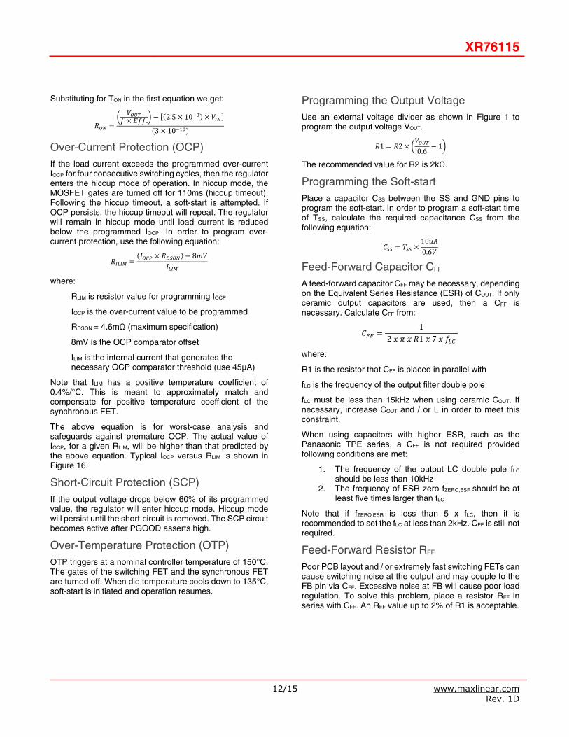
Selecting the DCM / CCM Mode In order to set the controller operation to DCM / CCM, a voltage between 3.1V and 5.5V must be applied to the EN/MODE pin. If an external control signal is available, it can be directly connected to the EN/MODE pin. In applications where an external control signal is not available, the EN/MODE input can be derived from VIN. If VIN is well regulated, use a resistor divider and set the voltage to 4.0V. If VIN varies over a wide range, the circuit shown in Figure 28 can be used to generate the required voltage.
Figure 27: Selecting Forced CCM by deriving EN/MODE from VIN
Figure 28: Selecting DCM/CCM by Deriving EN/MODE from VIN
Programming the On-Time The on-time TON is programmed via resistor RON according to following equation:
𝑅𝑅𝑂𝑂𝑂𝑂 =𝑉𝑉𝐼𝐼𝑂𝑂 × [𝑇𝑇𝑂𝑂𝑂𝑂 − (2.5 × 10⁻⁸)]
3 × 10⁻¹⁰
TON is calculated from:
𝑇𝑇𝑂𝑂𝑂𝑂 =𝑉𝑉𝑂𝑂𝑂𝑂𝑂𝑂
𝑉𝑉𝐼𝐼𝑂𝑂 × 𝑓𝑓 × 𝐸𝐸𝑓𝑓𝑓𝑓.
where:
f is the desired switching frequency at nominal IOUT
Eff. is the converter efficiency corresponding to nominal IOUT
XR76115
12/15 www.maxlinear.com Rev. 1D
Substituting for TON in the first equation we get:
𝑅𝑅𝑂𝑂𝑂𝑂 = 𝑉𝑉𝑂𝑂𝑂𝑂𝑂𝑂𝑓𝑓 × 𝐸𝐸𝑓𝑓𝑓𝑓. − [(2.5 × 10⁻⁸) × 𝑉𝑉𝐼𝐼𝑂𝑂]
(3 × 10⁻¹⁰)
Over-Current Protection (OCP) If the load current exceeds the programmed over-current IOCP for four consecutive switching cycles, then the regulator enters the hiccup mode of operation. In hiccup mode, the MOSFET gates are turned off for 110ms (hiccup timeout). Following the hiccup timeout, a soft-start is attempted. If OCP persists, the hiccup timeout will repeat. The regulator will remain in hiccup mode until load current is reduced below the programmed IOCP. In order to program over-current protection, use the following equation:
𝑅𝑅𝐼𝐼𝐼𝐼𝐼𝐼𝐼𝐼 =(𝐼𝐼𝑂𝑂𝑂𝑂𝑂𝑂 × 𝑅𝑅𝐷𝐷𝐷𝐷𝑂𝑂𝑂𝑂) + 8𝑚𝑚𝑉𝑉
𝐼𝐼𝐼𝐼𝐼𝐼𝐼𝐼
where:
RLIM is resistor value for programming IOCP
IOCP is the over-current value to be programmed
RDSON = 4.6mΩ (maximum specification)
8mV is the OCP comparator offset
ILIM is the internal current that generates the necessary OCP comparator threshold (use 45µA)
Note that ILIM has a positive temperature coefficient of 0.4%/°C. This is meant to approximately match and compensate for positive temperature coefficient of the synchronous FET.
The above equation is for worst-case analysis and safeguards against premature OCP. The actual value of IOCP, for a given RLIM, will be higher than that predicted by the above equation. Typical IOCP versus RLIM is shown in Figure 16.
Short-Circuit Protection (SCP) If the output voltage drops below 60% of its programmed value, the regulator will enter hiccup mode. Hiccup mode will persist until the short-circuit is removed. The SCP circuit becomes active after PGOOD asserts high.
Over-Temperature Protection (OTP) OTP triggers at a nominal controller temperature of 150°C. The gates of the switching FET and the synchronous FET are turned off. When die temperature cools down to 135°C, soft-start is initiated and operation resumes.
Programming the Output Voltage Use an external voltage divider as shown in Figure 1 to program the output voltage VOUT.
𝑅𝑅1 = 𝑅𝑅2 × 𝑉𝑉𝑂𝑂𝑂𝑂𝑂𝑂0.6
− 1
The recommended value for R2 is 2kΩ.
Programming the Soft-start Place a capacitor CSS between the SS and GND pins to program the soft-start. In order to program a soft-start time of TSS, calculate the required capacitance CSS from the following equation:
𝐶𝐶𝐷𝐷𝐷𝐷 = 𝑇𝑇𝐷𝐷𝐷𝐷 ×10𝑢𝑢𝑢𝑢0.6𝑉𝑉
Feed-Forward Capacitor CFF A feed-forward capacitor CFF may be necessary, depending on the Equivalent Series Resistance (ESR) of COUT. If only ceramic output capacitors are used, then a CFF is necessary. Calculate CFF from:
𝐶𝐶𝐹𝐹𝐹𝐹 =1
2 𝑥𝑥 𝜋𝜋 𝑥𝑥 𝑅𝑅1 𝑥𝑥 7 𝑥𝑥 𝑓𝑓𝐼𝐼𝑂𝑂
where:
R1 is the resistor that CFF is placed in parallel with
fLC is the frequency of the output filter double pole
fLC must be less than 15kHz when using ceramic COUT. If necessary, increase COUT and / or L in order to meet this constraint.
When using capacitors with higher ESR, such as the Panasonic TPE series, a CFF is not required provided following conditions are met:
1. The frequency of the output LC double pole fLC should be less than 10kHz
2. The frequency of ESR zero fZERO,ESR should be at least five times larger than fLC
Note that if fZERO,ESR is less than 5 x fLC, then it is recommended to set the fLC at less than 2kHz. CFF is still not required.
Feed-Forward Resistor RFF Poor PCB layout and / or extremely fast switching FETs can cause switching noise at the output and may couple to the FB pin via CFF. Excessive noise at FB will cause poor load regulation. To solve this problem, place a resistor RFF in series with CFF. An RFF value up to 2% of R1 is acceptable.
XR76115
13/15 www.maxlinear.com Rev. 1D
Maximum Allowable Voltage Ripple at FB Pin
Note that the steady-state voltage ripple at the feedback pin (VFB,RIPPLE) must not exceed 50mV in order for the controller to function correctly. If VFB,RIPPLE is larger than 50mV, then COUT should be increased as necessary in order to keep the VFB,RIPPLE below 50mV.
Thermal Design Proper thermal design is critical in controlling device temperatures and in achieving robust designs. There are a number of factors that affect the thermal performance. One key factor is the temperature rise of the devices in the package, which is a function of the thermal resistances of the devices inside the package and the power being dissipated.
The thermal resistance of the XR76115 is specified in the “Operating Ratings” section of this datasheet. The JEDEC θJA thermal resistance provided is based on tests that comply with the JESD51-2A “Integrated Circuit Thermal Test Method Environmental Conditions – Natural Convection” standard. JESD51-xx are a group of standards whose intent is to provide comparative data based on a standard test condition which includes a defined board construction. Since the actual board design in the final application will be different from the board defined in the standard, the thermal resistances in the final design may be different from those shown.
The package thermal derating curves for the XR76115 are shown in Figures 25 and 26. These correspond to input voltage of 12V and 5V, respectively.
Applications Circuit
Figure 29: XR76115 Application Circuit Schematic
CVCC 4.7uF
PWRGD
22uF
L1 IHLP-5050FD0.56uH @ 37A, 1.2mOhm
R12k,1%
R22k,1%
CSS 47nF
EN/MODE
CIN 0.1uF
VCC
R4 10k
CFF1nF
47uF
PVIN
VCC
D1 MMSZXXXX
RON 6k
FB
RFF10 Ohm
680uF
CBST1uF
SW RLIM 2.5k
47uF 47uF
Rsnb1 Ohm
Csnb 3.3nF
R3 10k,PVIN
PVIN
FB
XR76115
ILIM2
TON4EN3
SS5
VCC
11
AGN
D12
SW13
SW14
PGOOD6
FB7
AGND8
VIN
10
SW15
SW16
PGND 19
BST
37
PGND 21PGND 22PGND 23
SW 25PVIN 26PVIN 27
PVIN
29PV
IN30
PVIN
31PV
IN32
PVIN
33PV
IN34
SW36
PGND 20
AGND PAD
PGND PAD
SW P
ADPV
IN P
AD
NC9
NC1
SW17
SW18
PGND 24
PVIN 28
PVIN
35
600kHz 1.2V 15A
12VIN
22uF
MMSZ4687=4.3V --> DCM/CCM MMSZ4681=2.4V --> Forced CCM
XR76115
15/15 www.maxlinear.com Rev. 1D
Revision History
Revision Date Description
1A March 2014 Initial release: ECN 1413-14 03-26-2014
1B August 2015
Changed “On-Time 2” specification to: Min=170ns, Typ=200ns, Max= 230ns Changed “On-Time 3” specification to: Min=365ns, Typ=430ns, Max= 495ns Changed “f corresponding to On-Time 2” specification to: Min=362 kHz, Typ=417 kHz, Max= 490 kHz removed “f corresponding to On-Time 2” specifications for VOUT=3.3V, removed Diode Emulation Mode write up, modified Functional Block Diagram, modified Feed-Forward Capacitor write up, modified Programming the On-Time write up; added “Selecting the Forced CCM Mode”, “Selecting the DCM/CCM Mode”, “Feed-Forward Resistor”, “Maximum Allowable Voltage Ripple at FB Pin” sections
1C June 2018 Updated to MaxLinear logo. Updated format and Ordering Information table.
1D 10/18/19 Correct block diagram by changing the input gate into the Hiccup Mode from an AND gate to an OR gate. Update ordering information.
Corporate Headquarters: 5966 La Place Court Suite 100 Carlsbad, CA 92008 Tel.:+1 (760) 692-0711 Fax: +1 (760) 444-8598 www.maxlinear.com
The content of this document is furnished for informational use only, is subject to change without notice, and should not be construed as a commitment by MaxLinear, Inc. MaxLinear, Inc. assumes no responsibility or liability for any errors or inaccuracies that may appear in the informational content contained in this guide. Complying with all applicable copyright laws is the responsibility of the user. Without limiting the rights under copyright, no part of this document may be reproduced into, stored in, or introduced into a retrieval system, or transmitted in any form or by any means (electronic, mechanical, photocopying, recording, or otherwise), or for any purpose, without the express written permission of MaxLinear, Inc.
MaxLinear, Inc. does not recommend the use of any of its products in life support applications where the failure or malfunction of the product can reasonably be expected to cause failure of the life support system or to significantly affect its safety or effectiveness. Products are not authorized for use in such applications unless MaxLinear, Inc. receives, in writing, assurances to its satisfaction that: (a) the risk of injury or damage has been minimized; (b) the user assumes all such risks; (c) potential liability of MaxLinear, Inc. is adequately protected under the circumstances.
MaxLinear, Inc. may have patents, patent applications, trademarks, copyrights, or other intellectual property rights covering subject matter in this document. Except as expressly provided in any written license agreement from MaxLinear, Inc., the furnishing of this document does not give you any license to these patents, trademarks, copyrights, or other intellectual property.
MaxLinear, the MaxLinear logo, and any MaxLinear trademarks, MxL, Full-Spectrum Capture, FSC, G.now, AirPHY and the MaxLinear logo are all on the products sold, are all trademarks of MaxLinear, Inc. or one of MaxLinear’s subsidiaries in the U.S.A. and other countries. All rights reserved. Other company trademarks and product names appearing herein are the property of their respective owners.
© 2015 - 2019 MaxLinear, Inc. All rights reserved