Embed Size (px)
Citation preview
© Copyright 2015 WIZnet Co., Ltd. All rights reserved.
W7500 Datasheet Manual Version 1.0.0
http://www.wiznet.co.kr
W7500 Datasheet Version1.0.0 2 / 117
Table of Contents
1 Documentation conventions ........................................................................ 11
List of abbreviations ....................................................................... 11 1.1
Glossary ...................................................................................... 11 1.2
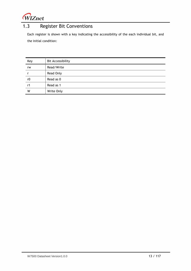
Register Bit Conventions .................................................................. 13 1.3
2 System and memory overview ..................................................................... 14
2.1 System architecture ....................................................................... 14
2.2 Memory organization ...................................................................... 15
Introduction ......................................................................... 15 2.2.1
Memory map ......................................................................... 16 2.2.2
3 System configuration controller (SYSCFG) ....................................................... 17
3.1 Introduction ................................................................................. 17
4 Interrupt and events ................................................................................. 17
4.1 Introduction ................................................................................. 17
4.2 Interrupt assignments ..................................................................... 17
4.3 Event ......................................................................................... 18
5 Power supply ........................................................................................... 18
5.1 Introduction ................................................................................. 18
5.2 Voltage regulator ........................................................................... 18
5.3 Power supply supervisor .................................................................. 19
5.4 Low-power modes .......................................................................... 19
Sleep mode .......................................................................... 19 5.4.1
Peripheral clock gating ............................................................ 20 5.4.2
6 System tick timer ..................................................................................... 20
6.1 Introduction ................................................................................. 20
6.2 Features ..................................................................................... 20
6.3 Functional description .................................................................... 20
7 TCPIPCore Offload Engine (TOE) ................................................................... 21
Introduction ................................................................................. 21 7.1
Features ..................................................................................... 21 7.2
Functional description .................................................................... 22 7.3
TOE Memory map ........................................................................... 22 7.4
Common register map ............................................................. 24 7.4.1
Socket register map ................................................................ 24 7.4.2
Memory ............................................................................... 25 7.4.3
8 Booting Sequence ..................................................................................... 27
9 Embedded Flash memory ............................................................................ 28
Flash main features ........................................................................ 28 9.1
W7500 Datasheet Version1.0.0 3 / 117
Flash memory functional description ................................................... 28 9.2
Flash memory organization ....................................................... 28 9.2.1
Read operations ..................................................................... 30 9.2.2
Flash erase operations ............................................................. 31 9.2.3
Flash program operation .......................................................... 33 9.2.4
Memory protection ......................................................................... 34 9.3
Read protection ..................................................................... 34 9.3.1
Write protection .................................................................... 34 9.3.2
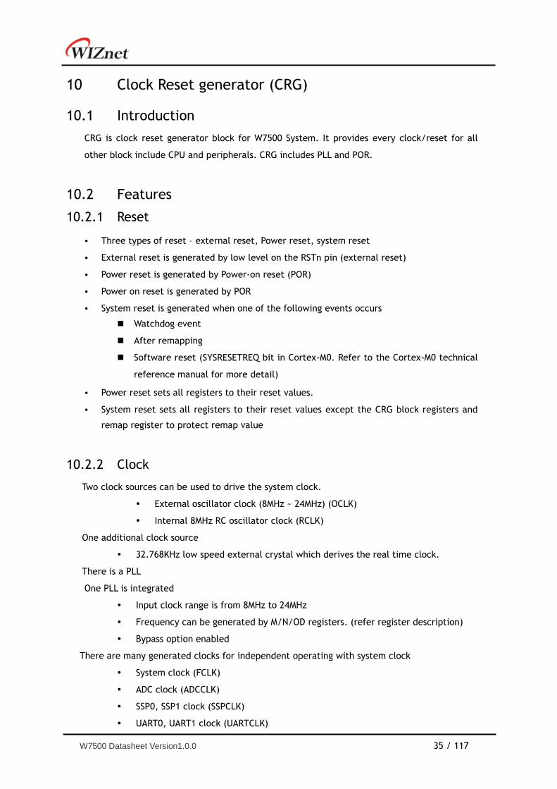
10 Clock Reset generator (CRG) ........................................................................ 35
10.1 Introduction ................................................................................. 35
10.2 Features ..................................................................................... 35
Reset .................................................................................. 35 10.2.1
Clock .................................................................................. 35 10.2.2
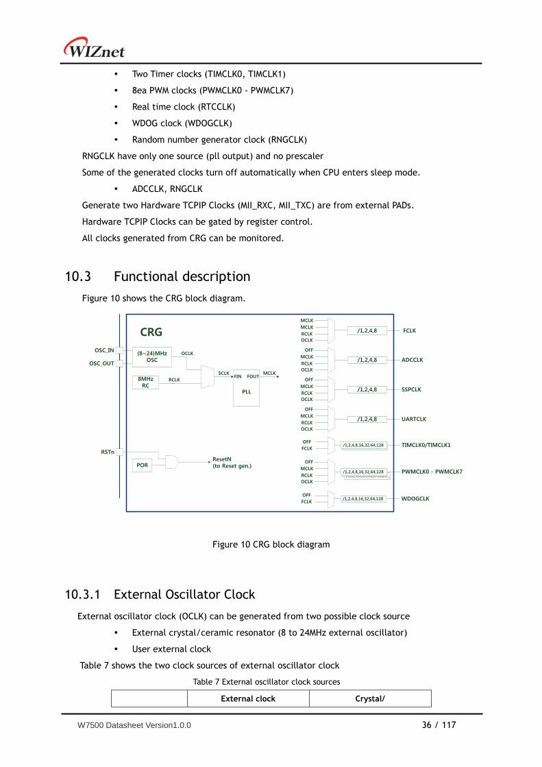
10.3 Functional description .................................................................... 36
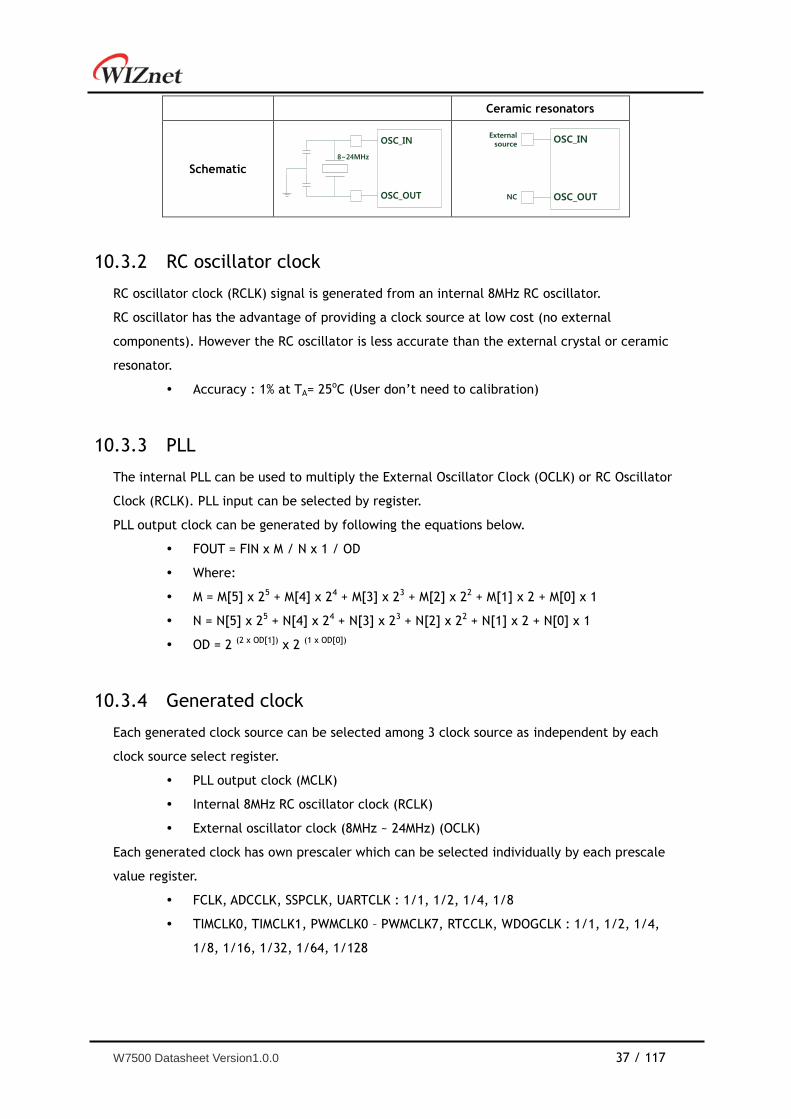
External Oscillator Clock .......................................................... 36 10.3.1
RC oscillator clock .................................................................. 37 10.3.2
PLL .................................................................................... 37 10.3.3
Generated clock .................................................................... 37 10.3.4
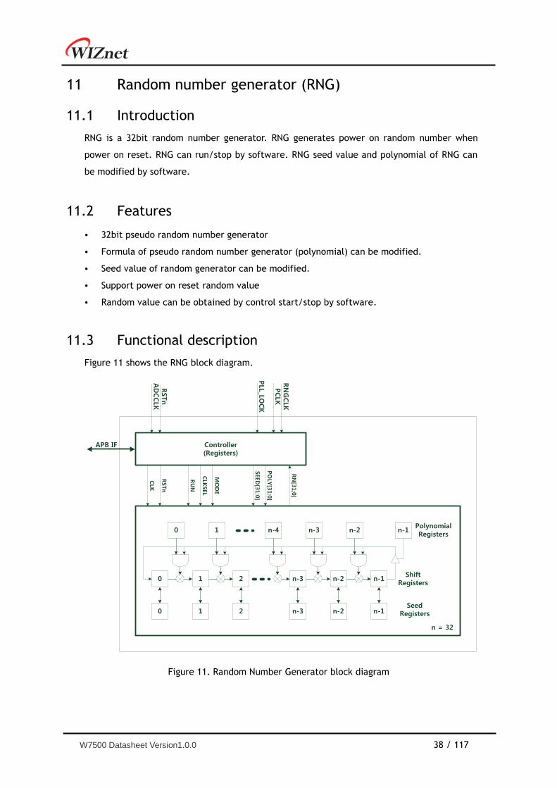
11 Random number generator (RNG) ................................................................. 38
Introduction ................................................................................. 38 11.1
Features ..................................................................................... 38 11.2
Functional description .................................................................... 38 11.3
Operation RNG ...................................................................... 39 11.3.1
12 Alternate Function Controller (AFC) .............................................................. 40
Introduction ................................................................................. 40 12.1
Features ..................................................................................... 40 12.2
Functional description .................................................................... 40 12.3
13 External Interrupt (EXTI) ............................................................................ 42
Introduction ................................................................................. 42 13.1
Features ..................................................................................... 42 13.2
Functional description .................................................................... 42 13.3
14 Pad Controller (PADCON) ............................................................................ 44
Introduction ................................................................................. 44 14.1
Features ..................................................................................... 44 14.2
Functional description .................................................................... 44 14.3
15 General-purpose I/Os(GPIO) ......................................................................... 45
Introduction ................................................................................. 45 15.1
Features ..................................................................................... 45 15.2
Functional description .................................................................... 46 15.3
W7500 Datasheet Version1.0.0 4 / 117
Masked access ....................................................................... 47 15.3.1
16 Direct memory access controller (DMA) .......................................................... 49
Introduction ................................................................................. 49 16.1
Features ..................................................................................... 49 16.2
Functional description .................................................................... 49 16.3
DMA request mapping .............................................................. 50 16.3.1
DMA arbitration ..................................................................... 50 16.3.2
DMA cycle types ..................................................................... 50 16.3.3
17 Analog-to-digital converter (ADC) ................................................................. 54
Introduction ................................................................................. 54 17.1
Features ..................................................................................... 54 17.2
Functional description .................................................................... 55 17.3
Operation ADC with non-interrupt ............................................... 55 17.3.1
Operation ADC with interrupt .................................................... 57 17.3.2
18 Pulse-Width Modulation (PWM) ..................................................................... 58
Introduction ................................................................................. 58 18.1
Features ..................................................................................... 58 18.2
Functional description .................................................................... 59 18.3
Timer/Counter control ............................................................ 59 18.3.1
Timer/Counter ...................................................................... 59 18.3.2
PWM mode ........................................................................... 63 18.3.3
Interrupt ............................................................................. 64 18.3.4
Dead zone generation ............................................................. 64 18.3.5
Capture event ....................................................................... 66 18.3.6
How to set the PWM ............................................................... 67 18.3.7
19 Dual timers ............................................................................................. 68
Introduction ................................................................................. 68 19.1
Features ..................................................................................... 68 19.2
Functional description .................................................................... 69 19.3
Clock and clock enable ............................................................ 69 19.3.1
Timer size ............................................................................ 69 19.3.2
Prescaler ............................................................................. 69 19.3.3
Repetition mode .................................................................... 69 19.3.4
Interrupt ............................................................................. 70 19.3.5
Operation ............................................................................ 70 19.3.6
How to set the dual timers ....................................................... 71 19.3.7
20 Watchdog timer ........................................................................................ 72
20.1 Introduction ................................................................................. 72
20.2 Features ..................................................................................... 72
W7500 Datasheet Version1.0.0 5 / 117
20.3 Functional description .................................................................... 72
Clock .................................................................................. 72 20.3.1
Interrupt and reset request ....................................................... 72 20.3.2
21 Inter-integrated circuit interface (I2C) ........................................................... 73
Introduction ................................................................................. 73 21.1
Features ..................................................................................... 73 21.2
Functional description .................................................................... 74 21.3
Data validity ......................................................................... 75 21.3.1
Acknowledge ........................................................................ 75 21.3.2
Bit Command Controller ........................................................... 75 21.3.3
Slave address ........................................................................ 77 21.3.4
Read/Write bit ...................................................................... 77 21.3.5
Acknowledge(ACK) and Not Acknowledge(NACK) ............................. 77 21.3.6
Data transfer ........................................................................ 77 21.3.7
Operating Modes .................................................................... 78 21.3.8
Interrupts ............................................................................ 79 21.3.9
Master mode ......................................................................... 80 21.3.10
Slave mode .......................................................................... 83 21.3.11
22 UART(Universal Asynchronous Receive Transmit) .............................................. 84
Introduction ................................................................................. 84 22.1
Features ..................................................................................... 84 22.2
Functional description .................................................................... 84 22.3
Baud rate calculation .............................................................. 86 22.3.1
Data transmission ................................................................... 87 22.3.2
Data receive ......................................................................... 87 22.3.3
Hardware flow control ............................................................. 88 22.3.4
23 Synchronous Serial Port (SSP) ...................................................................... 90
Introduction ................................................................................. 90 23.1
Features ..................................................................................... 90 23.2
Functional description .................................................................... 91 23.3
Clock prescaler ..................................................................... 91 23.3.1
Transmit FIFO ....................................................................... 91 23.3.2
Receive FIFO ......................................................................... 92 23.3.3
Interrupt generation logic ........................................................ 92 23.3.4
DMA interface ....................................................................... 92 23.3.5
Interface reset ...................................................................... 94 23.3.6
Configuring the SSP ................................................................ 94 23.3.7
Enable PrimeCell SSP operation .................................................. 94 23.3.8
Clock ratios .......................................................................... 95 23.3.9
W7500 Datasheet Version1.0.0 6 / 117
Programming the SSPCR0 Control Register ..................................... 96 23.3.10
Programming the SSPCR1 Control Register ..................................... 96 23.3.11
Frame format ....................................................................... 97 23.3.12
Texas Instruments synchronous serial frame format ......................... 98 23.3.13
Motorola SPI frame format ........................................................ 99 23.3.14
National Semiconductor Microwire frame format ........................... 105 23.3.15
Master and Slave configurations ................................................ 107 23.3.16
SSP Flow chart ..................................................................... 108 23.3.17
24 Electrical Characteristics .......................................................................... 110
Absolute maximum ratings .............................................................. 110 24.1
Voltage Characteristics ........................................................... 110 24.1.1
Current Characteristics ........................................................... 110 24.1.2
Thermal Characteristics .......................................................... 110 24.1.3
Operating conditions ..................................................................... 111 24.2
General Operating Conditions ................................................... 111 24.2.1
Supply Current Characteristics .................................................. 111 24.2.2
I/O PAD Characteristics .................................................................. 112 24.3
DC Specification ................................................................... 112 24.3.1
Flash memory .............................................................................. 112 24.4
Electrical Sensitivity Characteristics .................................................. 112 24.5
Electostatic discharge (ESD) ..................................................... 112 24.5.1
Static latch-up ..................................................................... 112 24.5.2
ADC Characteristics ....................................................................... 113 24.6
ADC Electrical characteristics ................................................... 113 24.6.1
ADC Transform function description ........................................... 114 24.6.2
I2C interface Characteristics ............................................................ 114 24.7
SSP Interface Characteristics ........................................................... 115 24.8
25 Package Characteristics ............................................................................ 116
Package dimension information ........................................................ 116 25.1
Package footprint information .......................................................... 116 25.2
Document History Information ....................................................................... 117
W7500 Datasheet Version1.0.0 7 / 117
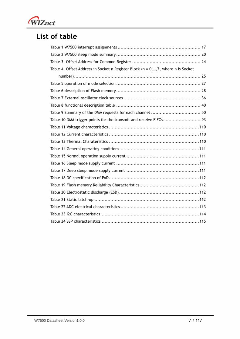
List of table
Table 1 W7500 interrupt assignments ......................................................... 17
Table 2 W7500 sleep mode summary .......................................................... 20
Table 3. Offset Address for Common Register ............................................... 24
Table 4. Offset Address in Socket n Register Block (n = 0,…,7, where n is Socket
number) ....................................................................................... 25
Table 5 operation of mode selection .......................................................... 27
Table 6 description of Flash memory .......................................................... 28
Table 7 External oscillator clock sources ..................................................... 36
Table 8 functional description table .......................................................... 40
Table 9 Summary of the DMA requests for each channel .................................. 50
Table 10 DMA trigger points for the transmit and receive FIFOs. ........................ 93
Table 11 Voltage characteristics .............................................................. 110
Table 12 Current characteristics .............................................................. 110
Table 13 Thermal Charateristics .............................................................. 110
Table 14 General operating conditions ...................................................... 111
Table 15 Normal operation supply current .................................................. 111
Table 16 Sleep mode supply current ......................................................... 111
Table 17 Deep sleep mode supply current .................................................. 111
Table 18 DC specification of PAD .............................................................. 112
Table 19 Flash memory Reliability Characteristics ......................................... 112
Table 20 Electrostatic discharge (ESD) ....................................................... 112
Table 21 Static latch-up ........................................................................ 112
Table 22 ADC electrical characteristics ...................................................... 113
Table 23 I2C characteristics .................................................................... 114
Table 24 SSP characteristics ................................................................... 115
W7500 Datasheet Version1.0.0 8 / 117
List of figures
Figure 1 W7500 System Architecture .......................................................... 14
Figure 2 W7500 memory map ................................................................... 16
Figure 3 POR reset waveform ................................................................... 19
Figure 4 TOE block diagram ..................................................................... 22
Figure 5. Register & Memory Organization ................................................... 23
Figure 6. operation of boot code .............................................................. 27
Figure 7. Flash reading sequence .............................................................. 31
Figure 8. Flash erase operations ............................................................... 32
Figure 9. main Flash memory programming sequence ..................................... 33
Figure 10 CRG block diagram ................................................................... 36
Figure 11. Random Number Generator block diagram ..................................... 38
Figure 12. Flow chart of RNG operation ...................................................... 39
Figure 13. External Interrupt diagram ........................................................ 43
Figure 14. function schematic of digital I/O pad ........................................... 44
Figure 15. function schematic of digital/analog mux IO pad ............................. 44
Figure 16. GPIO block diagram ................................................................. 46
Figure 17. GPIO Flow chart ..................................................................... 47
Figure 18. MASK LOWBYTE access ............................................................. 48
Figure 19. MASK HIGHBYTE access ............................................................. 48
Figure 20. DMA Block diagram .................................................................. 49
Figure 21. DMA ping pong cycle ................................................................ 53
Figure 22. ADC block diagram .................................................................. 55
Figure 23. The ADC operation flowchart with non-interrupt .............................. 56
Figure 24. The ADC operation flowchart with interrupt ................................... 57
Figure 25. PWM block diagram ................................................................. 58
Figure 26. Periodic mode ........................................................................ 59
Figure 27. one-shot mode ....................................................................... 60
Figure 28. Up-count mode ...................................................................... 60
Figure 29. Down-count mode ................................................................... 60
Figure 30 Counter mode with rising edge .................................................... 61
Figure 31 Counter mode with falling edge ................................................... 61
Figure 32 Counter mode with rising and falling edge ...................................... 61
Figure 33 Timer/Counter timing diagram with match interrupt ......................... 62
Figure 34 Timer/Counter timing diagram with overflow interrupt ...................... 62
Figure 35 The PWM output up to match register ............................................ 63
Figure 36 The PWM output up to limit register .............................................. 64
Figure 37 PWM waveform with dead zone time ............................................. 65
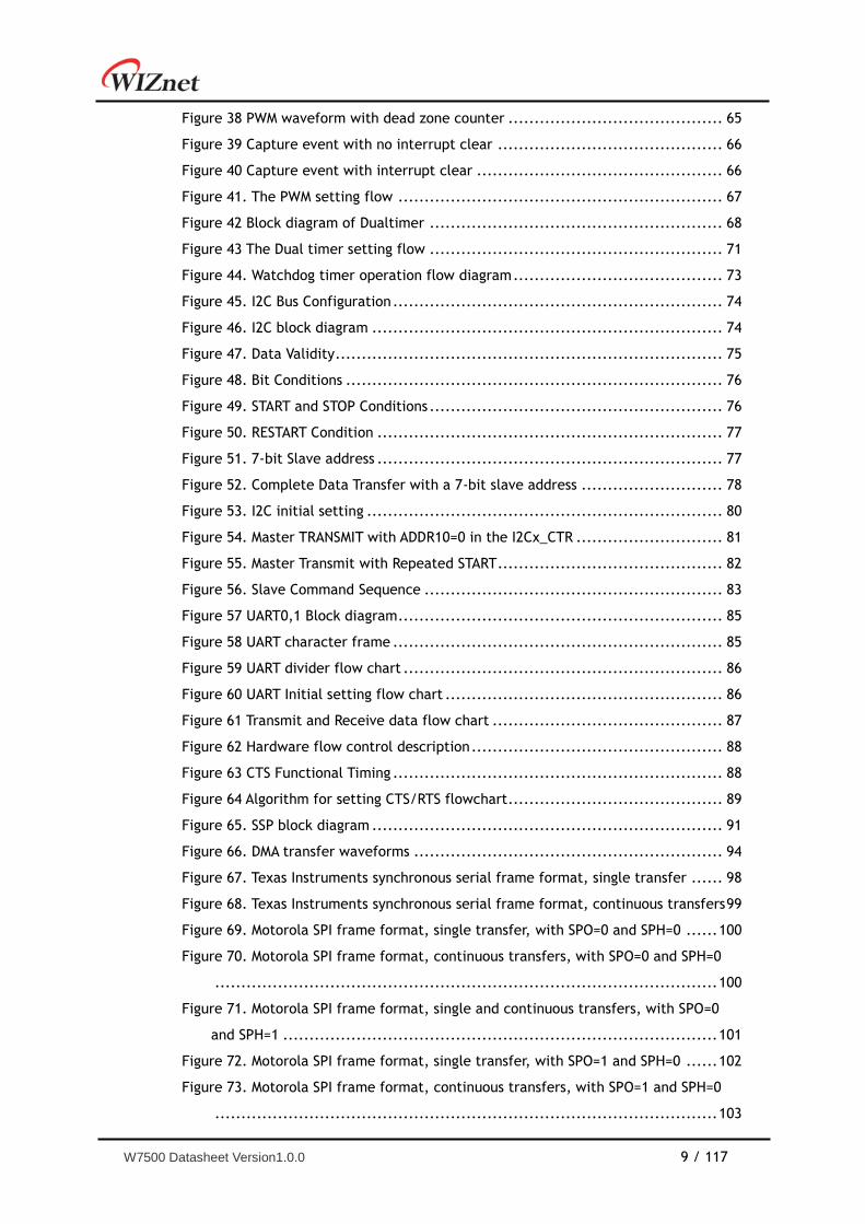
W7500 Datasheet Version1.0.0 9 / 117
Figure 38 PWM waveform with dead zone counter ......................................... 65
Figure 39 Capture event with no interrupt clear ........................................... 66
Figure 40 Capture event with interrupt clear ............................................... 66
Figure 41. The PWM setting flow .............................................................. 67
Figure 42 Block diagram of Dualtimer ........................................................ 68
Figure 43 The Dual timer setting flow ........................................................ 71
Figure 44. Watchdog timer operation flow diagram ........................................ 73
Figure 45. I2C Bus Configuration ............................................................... 74
Figure 46. I2C block diagram ................................................................... 74
Figure 47. Data Validity .......................................................................... 75
Figure 48. Bit Conditions ........................................................................ 76
Figure 49. START and STOP Conditions ........................................................ 76
Figure 50. RESTART Condition .................................................................. 77
Figure 51. 7-bit Slave address .................................................................. 77
Figure 52. Complete Data Transfer with a 7-bit slave address ........................... 78
Figure 53. I2C initial setting .................................................................... 80
Figure 54. Master TRANSMIT with ADDR10=0 in the I2Cx_CTR ............................ 81
Figure 55. Master Transmit with Repeated START ........................................... 82
Figure 56. Slave Command Sequence ......................................................... 83
Figure 57 UART0,1 Block diagram .............................................................. 85
Figure 58 UART character frame ............................................................... 85
Figure 59 UART divider flow chart ............................................................. 86
Figure 60 UART Initial setting flow chart ..................................................... 86
Figure 61 Transmit and Receive data flow chart ............................................ 87
Figure 62 Hardware flow control description ................................................ 88
Figure 63 CTS Functional Timing ............................................................... 88
Figure 64 Algorithm for setting CTS/RTS flowchart......................................... 89
Figure 65. SSP block diagram ................................................................... 91
Figure 66. DMA transfer waveforms ........................................................... 94
Figure 67. Texas Instruments synchronous serial frame format, single transfer ...... 98
Figure 68. Texas Instruments synchronous serial frame format, continuous transfers 99
Figure 69. Motorola SPI frame format, single transfer, with SPO=0 and SPH=0 ...... 100
Figure 70. Motorola SPI frame format, continuous transfers, with SPO=0 and SPH=0
................................................................................................ 100
Figure 71. Motorola SPI frame format, single and continuous transfers, with SPO=0
and SPH=1 ................................................................................... 101
Figure 72. Motorola SPI frame format, single transfer, with SPO=1 and SPH=0 ...... 102
Figure 73. Motorola SPI frame format, continuous transfers, with SPO=1 and SPH=0
................................................................................................ 103
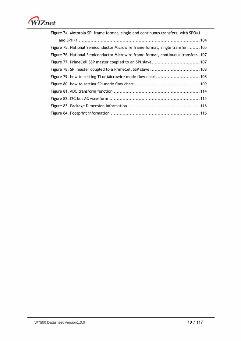
W7500 Datasheet Version1.0.0 10 / 117
Figure 74. Motorola SPI frame format, single and continuous transfers, with SPO=1
and SPH=1 ................................................................................... 104
Figure 75. National Semiconductor Microwire frame format, single transfer ........ 105
Figure 76. National Semiconductor Microwire frame format, continuous transfers . 107
Figure 77. PrimeCell SSP master coupled to an SPI slave ................................. 107
Figure 78. SPI master coupled to a PrimeCell SSP slave .................................. 108
Figure 79. how to setting TI or Microwire mode flow chart .............................. 108
Figure 80. how to setting SPI mode flow chart ............................................. 109
Figure 81. ADC transform function ........................................................... 114
Figure 82. I2C bus AC waveform .............................................................. 115
Figure 83. Package Dimension Information ................................................. 116
Figure 84. Footprint information ............................................................. 116
W7500 Datasheet Version1.0.0 11 / 117
1 Documentation conventions
List of abbreviations 1.1
Glossary 1.2
ARP Address Resolution Protocol
AHB Advanced High-performance Bus
AMBA Advanced Microcontroller Bus Architecture
APB Advanced Peripheral Bus
AFC Alternate Function Controller
ADC Analog-to-Digital Converter
BOD BrownOut Detection
CPU Central Processing Unit
CRG Clock Reset generator
DMA Direct Memory Access
EOP End Of Packet
EXTINT External Interrupt
GPIO General Purpose Input/Output
IrDA Infrared Data Association
I/O Input/Output
ICMP Internet Control Message Protocol
IGMP Internet Group Management Protocol
IPv4 Internet Protocol version 4
IRQ interrupt request
NMI NonMaskable Interrupt
PADCON Pad Controller
PLL Phase-Locked Loop
PHY Physical Layer
PPPoE Point-to-Point Protocol over Ethernet
POR Power Of Reset
PWM Pulse Width Modulator
RAM Random Access Memory
W7500 Datasheet Version1.0.0 12 / 117
RNG Random number generator
SR Status Register
SSP Synchronous Serial Port
SYSCFG System configuration controller
TOE TCPIPCore Offload Engine
TTL Transistor-Transistor Logic
TCP Transmission Control Protocol
UART Universal Asynchronous Receiver/Transmitter
USB Universal Serial Bus
UDP User Datagram Protocol
WOL Wake On Lan
WDT Watchdog Timer
W7500 Datasheet Version1.0.0 13 / 117
Register Bit Conventions 1.3
Each register is shown with a key indicating the accessibility of the each individual bit, and
the initial condition:
Key Bit Accessibility
rw Read/Write
r Read Only
r0 Read as 0
r1 Read as 1
W Write Only
W7500 Datasheet Version1.0.0 14 / 117
2 System and memory overview
2.1 System architecture
Main system consists of :
Two masters :
- Cortex-M0 core
- uDMAC (PL230, 6channel)
Ten slaves :
- Internal BOOT ROM
- Internal SRAM
- Internal Flash memory
- Two AHB2APB bridge which connects all APB peripherals
- Four AHB dedicated to 16bit GPIOs
- TCPIP Hardware core
System architecture and AHB-Lite bus architecture shown in Figure 1.
APBBridge
I2C
SPI x 2
UART
GPIO x 16
CM0
SWD
NVIC
ROM
AHB-Lite BUS
Flash (128KB)
FlashInterface
ROMController
SRAMController
SRAM(16KB)
uDMA(PL230)
TCP/IP
UART
SPI0/SPI1
I2C0/I2C1
GPIOA/GPIOBGPIOC/GPIOD
PAD Controller
PWM
WDOG
APBBridge
Alternate FunctionController
ADC
CRG
XTAL
ROSC
POR
Reset
PLL
ClocksResets
INTs
Ctrl
SRAM(32KB)
SRAM(4KB)
32K XTAL
UART0/UART1
Dual Timer0/Dual Timer1
APB B
US
FlashController
RNG
UART2
APBBridge
Figure 1 W7500 System Architecture
AHB-Lite BUS
- This bus connects the two masters (Cortex-M0 and uDMAC) and ten AHB
slaves.
W7500 Datasheet Version1.0.0 15 / 117
Two APB BUSs
- These buses connect Seventeen APB peripherals (Watchdog, two dual timers,
pwm, two UARTs, simple UART, two I2Cs, two SSPs, random number
generator, real time clock, 12bits analog digital converter, clock controller,
IO configuration, PAD MUX controller)
2.2 Memory organization
Introduction 2.2.1
Program memory, data memory, registers and I/O ports are organized within the same linear
4-Gbyte address space.
The bytes are coded in memory in Little Endian format. The lowest numbered byte in a word
is considered the word‟s least significant byte and the highest numbered byte the most
significant.
W7500 Datasheet Version1.0.0 16 / 117
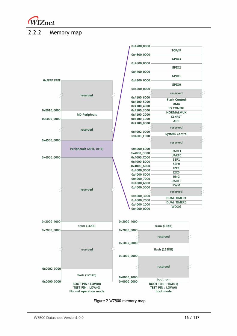
Memory map 2.2.2
flash (128KB)
0x0000_0000
0x0002_0000
sram (16KB)
reserved
0x2000_0000
0x2000_4000
reserved
0x4000_0000
Peripherals (APB, AHB)
WDOG0x4000_0000
0x4000_1000DUAL TIMER0
DUAL TIMER10x4000_2000
SSP0
0x4000_3000
SSP1
I2C0
0x4000_5000
reserved
M0 Periphrals
reserved
0xE000_0000
0xE010_0000
0xFFFF_FFFF
I2C1
0x4000_7000RNG
PWM
ADC
0x4000_6000
0x4000_8000
0x4000_9000
0x4000_B000
0x4000_A000
System Control
NORMALMUX
IO CONFIG
DMA
reserved
0x4200_0000
GPIO0
GPIO1
0x4300_0000
0x4600_0000
0x4500_0000
TCP/IP
0x4700_0000
0x4000_D000
BOOT PIN : LOW(0)TEST PIN : LOW(0)
Normal operation mode
boot rom0x0000_0000
0x0000_1000
reserved
reserved
0x1000_0000
sram (16KB)
0x1002_0000
reserved
0x2000_0000
flash (128KB)
0x2000_4000
BOOT PIN : HIGH(1)TEST PIN : LOW(0)
Boot mode
UART2
UART0
UART1
0x4000_C000
0x4000_E000
0x4001_F000
0x4002_0000
reserved
0x4100_0000
0x4100_1000CLKRST
0x4100_2000
0x4100_3000
0x4100_4000
0x4100_5000Flash Control
reserved
0x4100_6000
GPIO2
GPIO3
0x4400_0000
0x4500_0000
Figure 2 W7500 memory map
W7500 Datasheet Version1.0.0 17 / 117
3 System configuration controller (SYSCFG)
3.1 Introduction
Main purposes of the system configuration controller are the following
Control of the memory remap feature
The ability to enable an automatic reset if the system locks up
Information about the cause the last reset
4 Interrupt and events
4.1 Introduction
W7500 contains interrupt service and event service as below
26ea interrupt request (IRQ) lines.
One NonMaskable Interrupt (NMI).
One event signal
4.2 Interrupt assignments
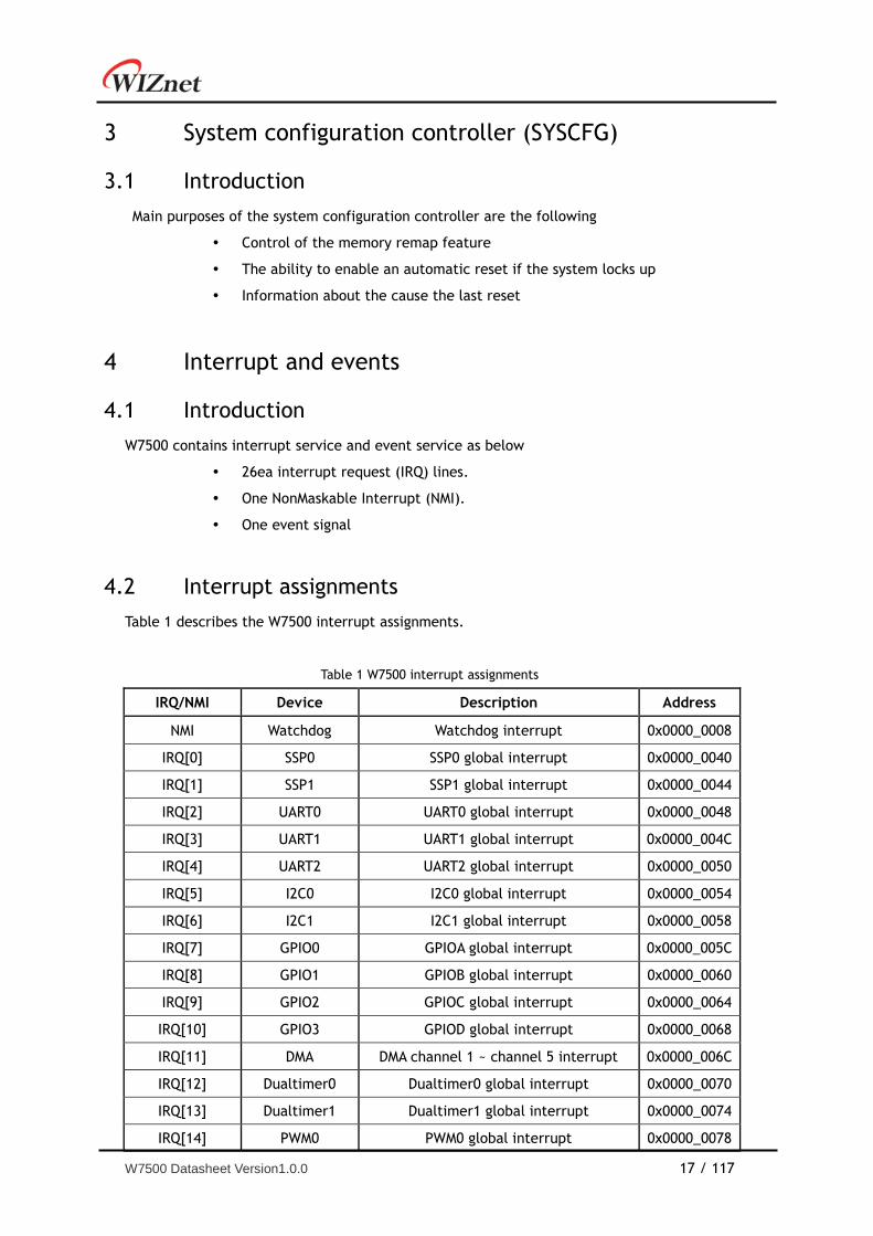
Table 1 describes the W7500 interrupt assignments.
Table 1 W7500 interrupt assignments
IRQ/NMI Device Description Address
NMI Watchdog Watchdog interrupt 0x0000_0008
IRQ[0] SSP0 SSP0 global interrupt 0x0000_0040
IRQ[1] SSP1 SSP1 global interrupt 0x0000_0044
IRQ[2] UART0 UART0 global interrupt 0x0000_0048
IRQ[3] UART1 UART1 global interrupt 0x0000_004C
IRQ[4] UART2 UART2 global interrupt 0x0000_0050
IRQ[5] I2C0 I2C0 global interrupt 0x0000_0054
IRQ[6] I2C1 I2C1 global interrupt 0x0000_0058
IRQ[7] GPIO0 GPIOA global interrupt 0x0000_005C
IRQ[8] GPIO1 GPIOB global interrupt 0x0000_0060
IRQ[9] GPIO2 GPIOC global interrupt 0x0000_0064
IRQ[10] GPIO3 GPIOD global interrupt 0x0000_0068
IRQ[11] DMA DMA channel 1 ~ channel 5 interrupt 0x0000_006C
IRQ[12] Dualtimer0 Dualtimer0 global interrupt 0x0000_0070
IRQ[13] Dualtimer1 Dualtimer1 global interrupt 0x0000_0074
IRQ[14] PWM0 PWM0 global interrupt 0x0000_0078
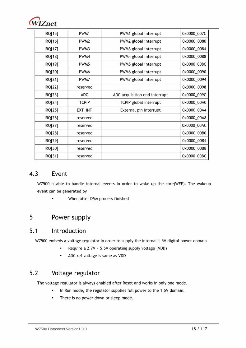
W7500 Datasheet Version1.0.0 18 / 117
IRQ[15] PWM1 PWM1 global interrupt 0x0000_007C
IRQ[16] PWM2 PWM2 global interrupt 0x0000_0080
IRQ[17] PWM3 PWM3 global interrupt 0x0000_0084
IRQ[18] PWM4 PWM4 global interrupt 0x0000_0088
IRQ[19] PWM5 PWM5 global interrupt 0x0000_008C
IRQ[20] PWM6 PWM6 global interrupt 0x0000_0090
IRQ[21] PWM7 PWM7 global interrupt 0x0000_0094
IRQ[22] reserved 0x0000_0098
IRQ[23] ADC ADC acquisition end interrupt 0x0000_009C
IRQ[24] TCPIP TCPIP global interrupt 0x0000_00A0
IRQ[25] EXT_INT External pin interrupt 0x0000_00A4
IRQ[26] reserved 0x0000_00A8
IRQ[27] reserved 0x0000_00AC
IRQ[28] reserved 0x0000_00B0
IRQ[29] reserved 0x0000_00B4
IRQ[30] reserved 0x0000_00B8
IRQ[31] reserved 0x0000_00BC
4.3 Event
W7500 is able to handle internal events in order to wake up the core(WFE). The wakeup
event can be generated by
When after DMA process finished
5 Power supply
5.1 Introduction
W7500 embeds a voltage regulator in order to supply the internal 1.5V digital power domain.
Require a 2.7V ~ 5.5V operating supply voltage (VDD)
ADC ref voltage is same as VDD
5.2 Voltage regulator
The voltage regulator is always enabled after Reset and works in only one mode.
In Run mode, the regulator supplies full power to the 1.5V domain.
There is no power down or sleep mode.
W7500 Datasheet Version1.0.0 19 / 117
5.3 Power supply supervisor
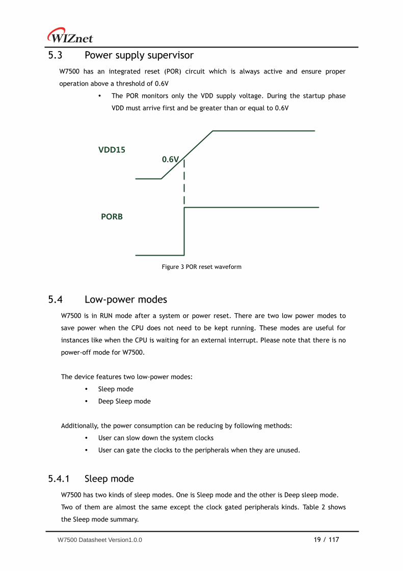
W7500 has an integrated reset (POR) circuit which is always active and ensure proper
operation above a threshold of 0.6V
The POR monitors only the VDD supply voltage. During the startup phase
VDD must arrive first and be greater than or equal to 0.6V
0.6VVDD15
PORB
Figure 3 POR reset waveform
5.4 Low-power modes
W7500 is in RUN mode after a system or power reset. There are two low power modes to
save power when the CPU does not need to be kept running. These modes are useful for
instances like when the CPU is waiting for an external interrupt. Please note that there is no
power-off mode for W7500.
The device features two low-power modes:
Sleep mode
Deep Sleep mode
Additionally, the power consumption can be reducing by following methods:
User can slow down the system clocks
User can gate the clocks to the peripherals when they are unused.
Sleep mode 5.4.1
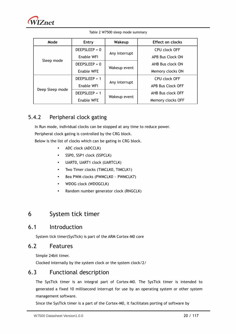
W7500 has two kinds of sleep modes. One is Sleep mode and the other is Deep sleep mode.
Two of them are almost the same except the clock gated peripherals kinds. Table 2 shows
the Sleep mode summary.
W7500 Datasheet Version1.0.0 20 / 117
Table 2 W7500 sleep mode summary
Mode Entry Wakeup Effect on clocks
Sleep mode
DEEPSLEEP = 0
Enable WFI Any interrupt
CPU clock OFF
APB Bus Clock ON
AHB Bus clock ON
Memory clocks ON
DEEPSLEEP = 0
Enable WFE Wakeup event
Deep Sleep mode
DEEPSLEEP = 1
Enable WFI Any interrupt
CPU clock OFF
APB Bus Clock OFF
AHB Bus clock OFF
Memory clocks OFF
DEEPSLEEP = 1
Enable WFE Wakeup event
Peripheral clock gating 5.4.2
In Run mode, individual clocks can be stopped at any time to reduce power.
Peripheral clock gating is controlled by the CRG block.
Below is the list of clocks which can be gating in CRG block.
ADC clock (ADCCLK)
SSP0, SSP1 clock (SSPCLK)
UART0, UART1 clock (UARTCLK)
Two Timer clocks (TIMCLK0, TIMCLK1)
8ea PWM clocks (PWMCLK0 ~ PWMCLK7)
WDOG clock (WDOGCLK)
Random number generator clock (RNGCLK)
6 System tick timer
6.1 Introduction
System tick timer(SysTick) is part of the ARM Cortex-M0 core
6.2 Features
Simple 24bit timer.
Clocked internally by the system clock or the system clock/2/
6.3 Functional description
The SysTick timer is an integral part of Cortex-M0. The SysTick timer is intended to
generated a fixed 10 millisecond interrupt for use by an operating system or other system
management software.
Since the SysTick timer is a part of the Cortex-M0, it facilitates porting of software by
W7500 Datasheet Version1.0.0 21 / 117
providing a standard timer that is available on Cortex-M0 based devices. The SysTick
timer can be used for :
An RTOS tick timer which fires at a programmable rate (for example 100 Hz) and
invokes a SysTick routine.
A high-speed alarm timer using the core clock.
A simple counter. Software can use this to measure time to completion and time
used.
An internal clock source control based on missing/meeting durations. The
COUNTFLAG bit-field in the control and status register can be used to determine if
an action completed within a set duration, as part of a dynamic clock management
control loop.
7 TCPIPCore Offload Engine (TOE)
Introduction 7.1
The TCP/IPCore Offlead Engine (TOE) is a Hardwired TCP/IP embedded Ethernet controller
that provides easier Internet connection to embedded systems. TOE enables users to have
Internet connectivity in their applications by using the TCP/IP stack.
WIZnet„s Hardwired TCP/IP is the market-proven technology that supports TCP, UDP, IPv4,
ICMP, ARP, IGMP, and PPPoE protocols. TOE embeds the 32Kbyte internal memory buffer for
the Ethernet packet processing. Using TOE allows users to implement the Ethernet
application by adding the simple socket program. It‟s faster and easier than using any other
Embedded Ethernet solutions. 8 independent hardware sockets can be used simultaneously.
TOE also provides WOL (Wake on LAN) to reduce power consumption of the system.
Features 7.2
Supports Hardwired TCP/IP Protocols : TCP, UDP, ICMP, IPv4, ARP, IGMP, PPPoE
Supports 8 independent sockets simultaneously
Supports Power down mode
Supports Wake on LAN over UDP
Internal 32Kbytes Memory for TX/RX Buffers
Not supports IP Fragmentation
W7500 Datasheet Version1.0.0 22 / 117
Functional description 7.3
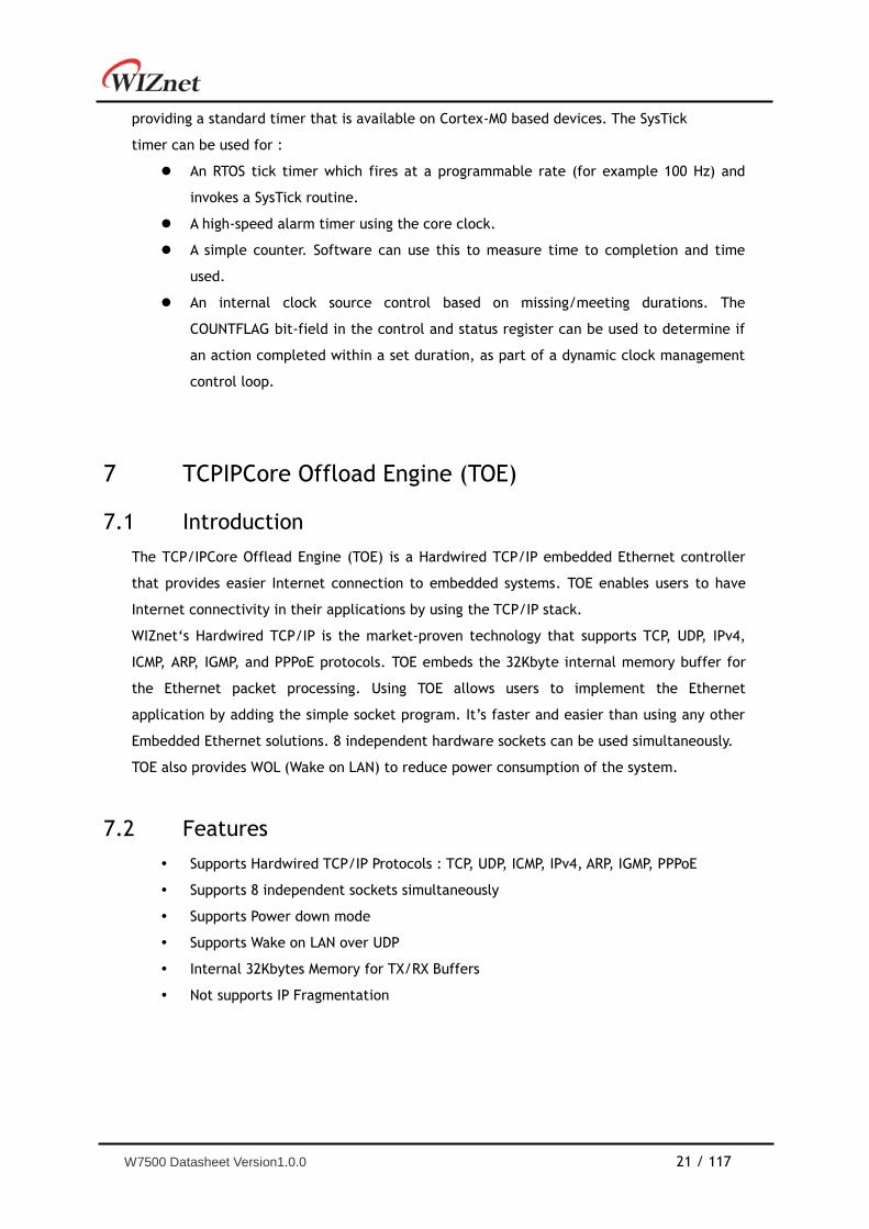
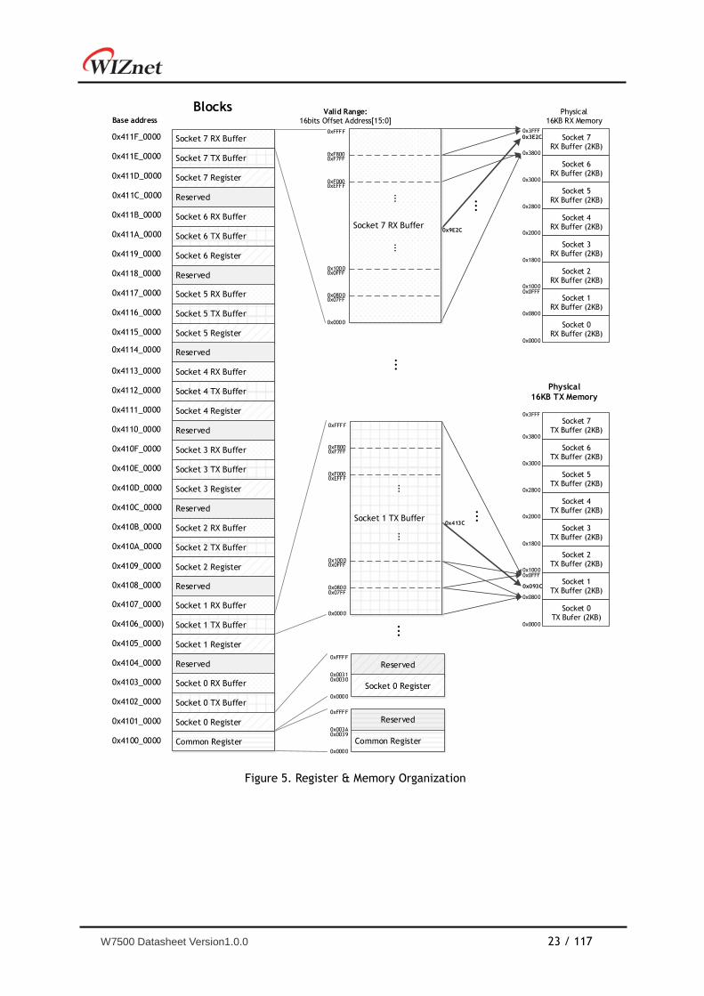
Figure 4 shows the TOE block diagram.
Figure 4 TOE block diagram
TOE Memory map 7.4
TOE has one Common Register Block, eight Socket Register Blocks, and TX/RX Buffer Blocks
allocated to each Socket. Figure 5 shows the selected block by the base address and the
available offset address range of Socket TX/RX Buffer Blocks. Each Socket‟s TX Buffer Block
physically exists in one 16KB TX memory and is initially allocated with 2KB. Also, Each
Socket‟s RX Buffer Block physically exists in one 16KB RX Memory and is initially allocated
with 2KB.
Regardless of the allocated size of each Socket TX/RX Buffer, it can be accessible within the
16 bits offset address range (From 0x0000 to 0xFFFF).
Refer to „Chapter 7.4.3‟ for more information about 16KB TX/RX Memory organization and
access method.
RXCTXCRXC_NTXC_NCOLDUPCRSRXDVRXD[3:0]TXETXD[3:0]
MDCMDOMDI
CommonRegister
SocketRegister
Register Controller
Memory Controller
TXMemory
RXMemory
TCPIPCore
MDCControllerINT
MIIController
AHB
W7500 Datasheet Version1.0.0 23 / 117
Figure 5. Register & Memory Organization
Base address
Blocks Physical 16KB RX Memory
Valid Range:16bits Offset Address[15:0]
...
0x411F_0000
0x411E_0000
0x411D_0000
0x411C_0000
0x411B_0000
0x411A_0000
0x4119_0000
0x4118_0000
0x4117_0000
0x4116_0000
0x4115_0000
0x4113_0000
0x4112_0000
0x4111_0000
0x4110_0000
0x410F_0000
0x410E_0000
0x410D_0000
0x410C_0000
0x410B_0000
0x410A_0000
0x4109_0000
0x4108_0000
0x4107_0000
0x4106_0000)
0x4105_0000
0x4103_0000
0x4102_0000
0x4101_0000
0x4100_0000
0x4104_0000
0x4114_0000
Reserved
Reserved
Socket 1 TX Buffer
......
Socket 7 RX Buffer
......
...
...
0x0000
0x1000
0x0800
0x1800
0x2000
0x2800
0x3000
0x3800
0x3FFF
Socket 0TX Bufer (2KB)
Socket 1TX Buffer (2KB)
Socket 2TX Buffer (2KB)
Socket 3TX Buffer (2KB)
Socket 4TX Buffer (2KB)
Socket 5TX Buffer (2KB)
Socket 6TX Buffer (2KB)
Socket 7TX Buffer (2KB)
0x093C
0x0FFF
...
0x0000
0x1000
0x0800
0x1800
0x2000
0x2800
0x3000
0x3800
0x3FFF
Socket 0RX Buffer (2KB)
Socket 1RX Buffer (2KB)
Socket 2RX Buffer (2KB)
Socket 3RX Buffer (2KB)
Socket 4RX Buffer (2KB)
Socket 5RX Buffer (2KB)
Socket 6RX Buffer (2KB)
Socket 7 RX Buffer (2KB)
0x3E2C
0x0FFF
Physical
16KB TX Memory
Socket 7 RX Buffer
Socket 7 TX Buffer
Socket 7 Register
Reserved
Socket 6 RX Buffer
Socket 6 TX Buffer
Socket 6 Register
Reserved
Socket 5 RX Buffer
Socket 5 TX Buffer
Socket 5 Register
Reserved
Socket 4 RX Buffer
Socket 4 TX Buffer
Socket 4 Register
Reserved
Socket 3 RX Buffer
Socket 3 TX Buffer
Socket 3 Register
Reserved
Socket 2 RX Buffer
Socket 2 TX Buffer
Socket 2 Register
Reserved
Socket 1 RX Buffer
Socket 1 TX Buffer
Socket 1 Register
Reserved
Socket 0 RX Buffer
Socket 0 TX Buffer
Socket 0 Register
Common Register0x0000
0x00390x003A
0xFFFF
0x0000
0x00300x0031
0xFFFF
0x0000
0x07FF0x0800
0xFFFF
0x0FFF0x1000
0xEFFF0xF000
0xF7FF0xF800
0x0000
0x07FF0x0800
0xFFFF
0x0FFF0x1000
0xEFFF0xF000
0xF7FF0xF800
0x413C
0x9E2C
Socket 0 Register
Common Register
W7500 Datasheet Version1.0.0 24 / 117
Common register map 7.4.1
Common Register Block configures the general information of TOE such as IP and MAC
address. <Table 3> defines the offset address of registers in this block. Refer to „Chapter
7.4.1‟ for more details about each register.
Table 3. Offset Address for Common Register
Address Register
0x0000 TOE Version (VERSIONR)
0x2000 TICKCLOK (TCLKR)
0x2100 Interrupt (IR)
0x2104 Interrupt Mask (IMR)
0x2108 Interrupt Clear (IRCR)
0x2110 Socket Interrupt (SIR)
0x2114 Socket Mask (SIMR)
0x2300 Mode (MR)
0x2400 PPP Timer (PTIMER)
0x2404 PPP Magic (PMAGIC)
0x2408 PPP Destination MAC Address (PHAR1)
0x240C PPP Destination MAC address (PHAR0)
0x2410 PPP Session Identification (PSID)
0x2414 PPP Maximum Segment Size (PMSS)
0x6000 Source Hardware Address (SHAR1)
0x6004 Source Hardware Address (SHAR0)
0x6008 Gateway Address (GA)
0x600C Subnet Mask (SUB)
0x6010 Source IP Address (SIP)
0x6020 Network Configuration Lock (NCONFL)
0x6040 Retry Time (RTR)
0x6044 Retry Counter (RCR)
0x6050 Unreachable IP Address (UIP)
0x6054 Unreachable Port Address (UPORT)
Socket register map 7.4.2
TOE supports 8 Sockets for communication channel. Each Socket is controlled by Socket n
Register (n = 0,…,7 ,where n is socket number). <Table 2> defines the 16bits Offset Address
of registers in Socket n Register Block.
Refer to „Chapter 7.4.2‟ for more details about each register.
W7500 Datasheet Version1.0.0 25 / 117
Table 4. Offset Address in Socket n Register Block (n = 0,…,7, where n is Socket number)
Offset Register
0x0000 Socket Mode (Sn_MR)
0x0010 Socket Command (Sn_CR)
0x0020 Socket Interrupt (Sn_IR)
0x0024 Socket Interrupt Mask (Sn_IMR)
0x0028 Socket Interrupt Clear (Sn_ICR)
0x0030 Socket Status (Sn_SR)
0x0100 Socket Protocol Number (Sn_PNR)
0x0104 Socket IP Type of Service (Sn_TOS)
0x0108 Socket TTL (Sn_TTLR)
0x010C Socket Fragment Offset (Sn_FRAG)
0x0110 Socket Maximum Segment (Sn_MSSR)
0x0114 Socket Port Number (Sn_PORT)
0x0118 Socket Destination Hardware address0 (Sn_DHAR0)
0x011C Socket Destination Hardware address1 (Sn_DHAR1)
0x0120 Socket Destination Port Number (Sn_DPORTR)
0x0124 Socket Destination IP Address (Sn_DIPR)
0x0180 Socket Keep Alive Timer (Sn_KATMR)
0x0184 Socket Retry Time (Sn_RTR)
0x0188 Socket Retry Counter (Sn_RCR)
0x0200 Socket TX Memory Size (Sn_TXBUF_SIZE)
0x0204 Socket TX Free Size (Sn_TX_FSR)
0x0208 Socket TX Read Pointer (Sn_TX_RD)
0x020C Socket TX Write Pointer (Sn_TX_WR)
0x0220 Socket RX Memory Size (Sn_RXBUF_SIZE)
0x0224 Socket RX Received Size (Sn_RX_RSR)
0x0228 Socket RX Read Pointer (Sn_RX_RD)
0x022C Socket RX Write Pointer (Sn_RX_WR)
Memory 7.4.3
TOE has one 16KB TX memory for Socket n TX Buffer Blocks and one 16KB RX memory for
Socket n RX buffer Blocks.
16KB TX memory is initially allocated in 2KB size for each Socket TX Buffer Block (2KB X 8 =
16KB). The initial allocated 2KB size of Socket n TX Buffer can be re-allocated by using
„Socket n TX Buffer Size Register (Sn_TXBUF_SIZE)‟.
W7500 Datasheet Version1.0.0 26 / 117
Once all Sn_TXBUF_SIZE registers have been configured, Socket TX Buffer is allocated with
the configured size of 16KB TX Memory and is assigned sequentially from Socket 0 to Socket
7. Its physical memory address is automatically determined in 16KB TX memory. Therefore,
the total sum of Sn_TXBUF_SIZE should not exceed 16 in case of error in data transmission.
The 16KB RX memory allocation method is the same as the 16KB TX memory allocation
method. 16KB RX memory is initially allocated into 2KB size for each Socket RX Buffer Block
(2KB X 8 = 16KB). The initial allocated 2KB size of Socket n RX Buffer can be re-allocated by
using „Socket n RX Buffer Size Register (Sn_RXBUF_SIZE)‟.
When all Sn_RXBUF_SIZE registers have been configured, the Socket RX Buffer is allocated
with the configured size in 16KB RX Memory and is assigned sequentially from Socket 0 to
Socket 7. The physical memory address of the Socket RX Buffer is automatically determined
in 16KB RX memory. Therefore, the total sum of Sn_RXBUF_SIZE should not exceed 16 or data
reception error will occur.
For 16KB TX/RX memory allocation, refer to Sn_TXBUF_SIZE & Sn_RXBUF_SIZE in „Chapter
7.4.2‟ . The Socket n TX Buffer Block allocated in 16KB TX memory is buffer for saving data
to be transmitted by host. The 16bits Offset Address of Socket n TX Buffer Block has 64KB
address space ranged from 0x0000 to 0xFFFF, and is configured with reference to „Socket n
TX Write Pointer Register (Sn_TX_WR)‟ & „Socket n TX Read Pointer Register(Sn_RX_RD)‟.
However, the 16bits Offset Address automatically converts into the physical address to be
accessible in 16KB TX memory such as Figure 5. Refer to „Chapter 7.4.2‟ for Sn_TX_WR &
Sn_TX_RD.
The Socket n RX Buffer Block allocated in 16KB RX memory is buffer for saving the received
data through the Ethernet. The 16bits Offset Address of Socket n RX Buffer Block has 64KB
address space ranged from 0x0000 to 0xFFFF, and is configured with reference to „Socket n
RX RD Pointer Register (Sn_RX_RD)‟ & „Socket n RX Write Pointer Register (Sn_RX_WR)‟.
However, the 16bits Offset Address automatically converts into the physical address to be
accessible in 16KB RX memory such as Figure 5. Refer to „Chapter 7.4.2‟ for Sn_RX_RD &
Sn_RX_WR.
W7500 Datasheet Version1.0.0 27 / 117
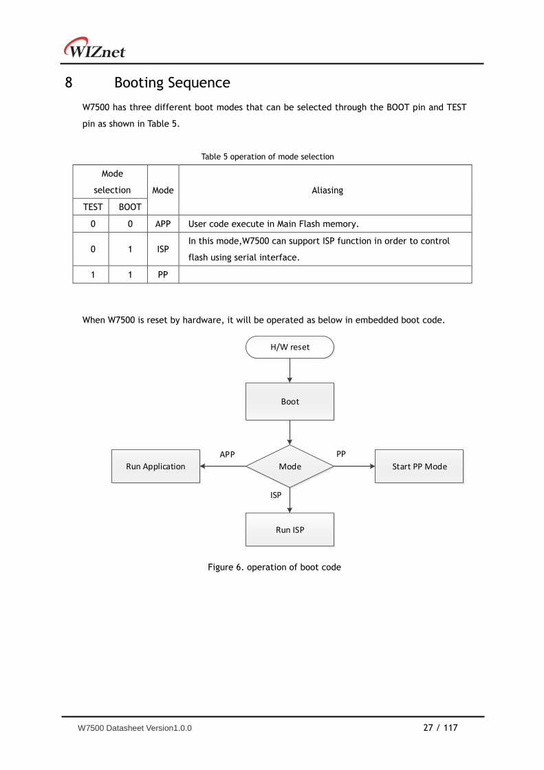
8 Booting Sequence
W7500 has three different boot modes that can be selected through the BOOT pin and TEST
pin as shown in Table 5.
Table 5 operation of mode selection
Mode
selection Mode Aliasing
TEST BOOT
0 0 APP User code execute in Main Flash memory.
0 1 ISP In this mode,W7500 can support ISP function in order to control
flash using serial interface.
1 1 PP
When W7500 is reset by hardware, it will be operated as below in embedded boot code.
H/W reset
Boot
Mode Start PP Mode
PP
Run Application
APP
ISP
Run ISP
Figure 6. operation of boot code
W7500 Datasheet Version1.0.0 28 / 117
9 Embedded Flash memory
Flash main features 9.1
Up to 128Kbytes of Flash memory
Memory organization:
Main Flash memory block:
Up to 128Kbytes
Information block:
Up to 512bytes
Information block is read only
Data block:
Up to 512bytes
Flash memory interface features:
Read interface with prefetch buffer( 1 x 32-bit words )
Flash Program / Erase operation
Read / Write protection
Flash memory functional description 9.2
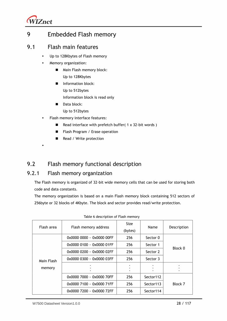
Flash memory organization 9.2.1
The Flash memory is organized of 32-bit wide memory cells that can be used for storing both
code and data constants.
The memory organization is based on a main Flash memory block containing 512 sectors of
256byte or 32 blocks of 4Kbyte. The block and sector provides read/write protection.
Table 6 description of Flash memory
Flash area Flash memory address Size
(bytes) Name Description
Main Flash
memory
0x0000 0000 ~ 0x0000 00FF 256 Sector 0
Block 0 0x0000 0100 ~ 0x0000 01FF 256 Sector 1
0x0000 0200 ~ 0x0000 02FF 256 Sector 2
0x0000 0300 ~ 0x0000 03FF 256 Sector 3
. .
.
. .
.
. .
.
. .
.
0x0000 7000 ~ 0x0000 70FF 256 Sector112
Block 7 0x0000 7100 ~ 0x0000 71FF 256 Sector113
0x0000 7200 ~ 0x0000 72FF 256 Sector114
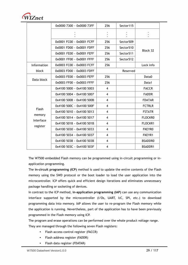
W7500 Datasheet Version1.0.0 29 / 117
0x0000 7300 ~ 0x0000 73FF 256 Sector115
. .
.
. .
.
. .
.
. .
.
0x0001 FC00 ~ 0x0001 FCFF 256 Sector509
Block 32 0x0001 FD00 ~ 0x0001 FDFF 256 Sector510
0x0001 FE00 ~ 0x0001 FEFF 256 Sector511
0x0001 FF00 ~ 0x0001 FFFF 256 Sector512
Information
block
0x0003 FC00 ~ 0x0003 FCFF 256 Lock info
0x0003 FD00 ~ 0x0003 FDFF Reserved
Data block 0x0003 FE00 ~ 0x0003 FEFF 256 Data0
0x0003 FF00 ~ 0x0003 FFFF 256 Data1
Flash
memory
Interface
register
0x4100 5000 ~ 0x4100 5003 4 FACCR
0x4100 5004 ~ 0x4100 5007 4 FADDR
0x4100 5008 ~ 0x4100 500B 4 FDATAR
0x4100 500C ~ 0x4100 500F 4 FCTRLR
0x4100 5010 ~ 0x4100 5013 4 FSTATR
0x4100 5014 ~ 0x4100 5017 4 FLOCKR0
0x4100 5018 ~ 0x4100 501B 4 FLOCKR1
0x4100 5030 ~ 0x4100 5033 4 FKEYR0
0x4100 5034 ~ 0x4100 5037 4 FKEYR1
0x4100 5038 ~ 0x4100 503B 4 BSADDR0
0x4100 503C ~ 0x4100 503F 4 BSADDR1
The W7500 embedded Flash memory can be programmed using in-circuit programming or in-
application programming.
The in-circuit programming (ICP) method is used to update the entire contents of the Flash
memory using the SWD protocol or the boot loader to load the user application into the
microcontroller. ICP offers quick and efficient design iterations and eliminates unnecessary
package handling or socketing of devices.
In contrast to the ICP method, in-application programming (IAP) can use any communication
interface supported by the microcontroller (I/Os, UART, I2C, SPI, etc.) to download
programming data into memory. IAP allows the user to re-program the Flash memory while
the application is running. Nevertheless, part of the application has to have been previously
programmed in the Flash memory using ICP.
The program and erase operations can be performed over the whole product voltage range.
They are managed through the following seven Flash registers:
Flash access control register (FACCR)
Flash address register (FADDR)
Flash data register (FDATAR)
W7500 Datasheet Version1.0.0 30 / 117
Flash control register (FCTRLR)
Flash status register (FSTATR)
Flash lock register (FLOCKR0/R1)
Flash key register (FKEYR0/R1)
Unlocking the Flash access Control register (FACCR)
After reset, the Flash memory is protected against unwanted write or erase operations. The
FACCR register is not accessible in write mode. An unlocking sequence should be written to
the FKEYR0/R1 register to open the access to the FACCR register. This sequence consists of
two write operations:
Write KEY 0 (FKEYR0) = 0x52537175
Write KEY 1 (FKEYR1) = 0xA91875FC
Any wrong sequence locks up the FACCR register.
The FACCR register can be locked again by finishing flash control operation.
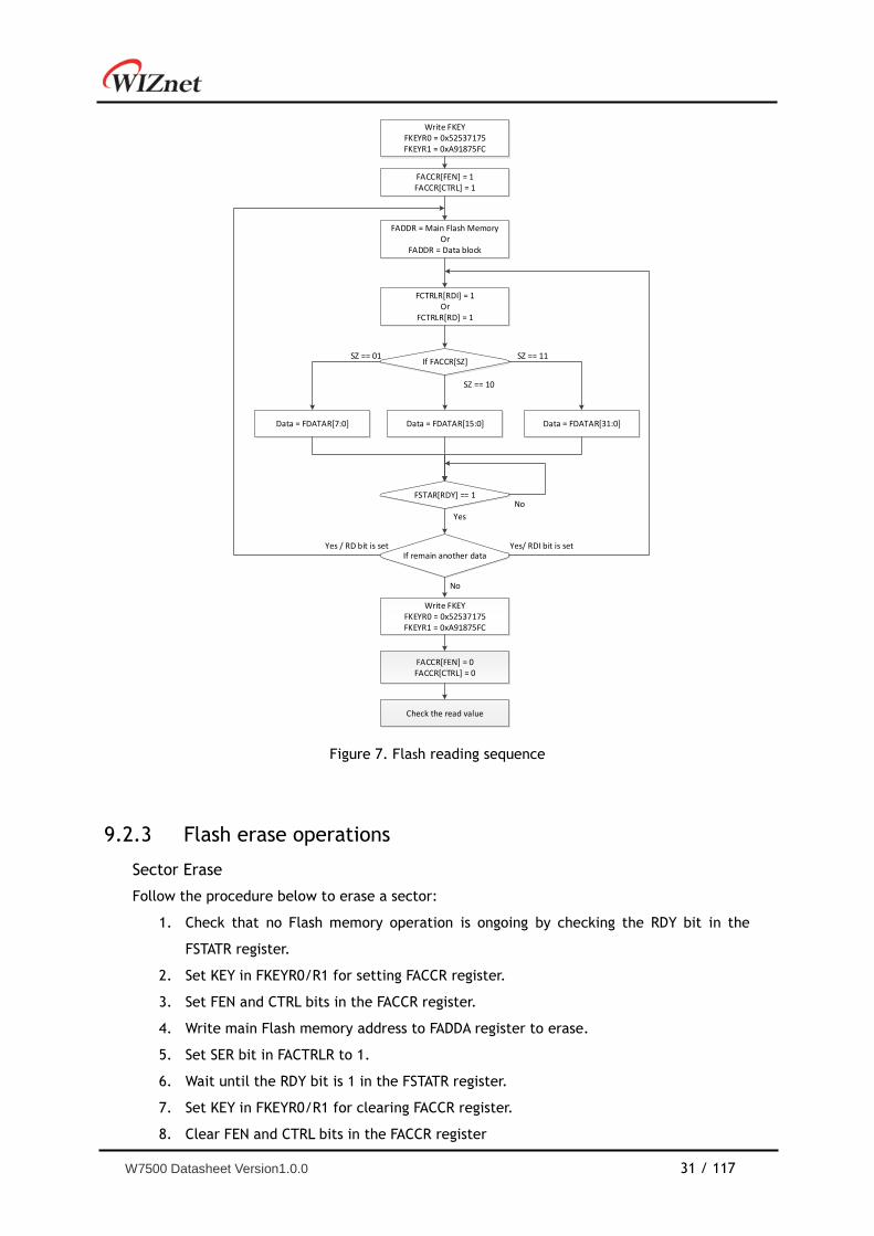
Read operations 9.2.2
The embedded Flash module can be addressed directly as a common memory space. Any
data read operation accesses the content of the Flash module through dedicated read senses
and provides the requested data.
The instruction fetch and the data access are both done through the same AHB bus. Read
accesses can be performed with the following options managed through the Flash control
register. (FCTRLR)
The Flash reading sequence using FCTRLR register is as below:
1. Check that no main Flash memory operation is ongoing by checking the RDY bit in
the FSTATR register.
2. Set KEY in FKEYR0/R1 for setting FACCR register.
3. Set FEN and CTRL bits in the FACCR register.
4. Write main Flash memory address or Data block address to FADDR register.
5. Set RDI or RD bit in FACTRLR to 1. If use RDI bit, don‟t need to set FADDR again due
to increase automatically by SZ bit in FACCR register.
6. Read data from FDATAR register.
7. Wait until the RDY bit is 1 in the FSTATR register.( it is set when the programming
operation has succeeded)
8. Set KEY in FKEYR0/R1 for clearing FACCR register.
9. Clear FEN and CTRL bits in the FACCR register
W7500 Datasheet Version1.0.0 31 / 117
Write FKEYFKEYR0 = 0x52537175FKEYR1 = 0xA91875FC
FACCR[FEN] = 1FACCR[CTRL] = 1
FADDR = Main Flash MemoryOr
FADDR = Data block
FSTAR[RDY] == 1No
Yes
If remain another dataYes/ RDI bit is setYes / RD bit is set
No
Check the read value
FACCR[FEN] = 0FACCR[CTRL] = 0
Write FKEYFKEYR0 = 0x52537175FKEYR1 = 0xA91875FC
If FACCR[SZ]
Data = FDATAR[7:0] Data = FDATAR[15:0] Data = FDATAR[31:0]
SZ == 01 SZ == 11
SZ == 10
FCTRLR[RDI] = 1Or
FCTRLR[RD] = 1
Figure 7. Flash reading sequence
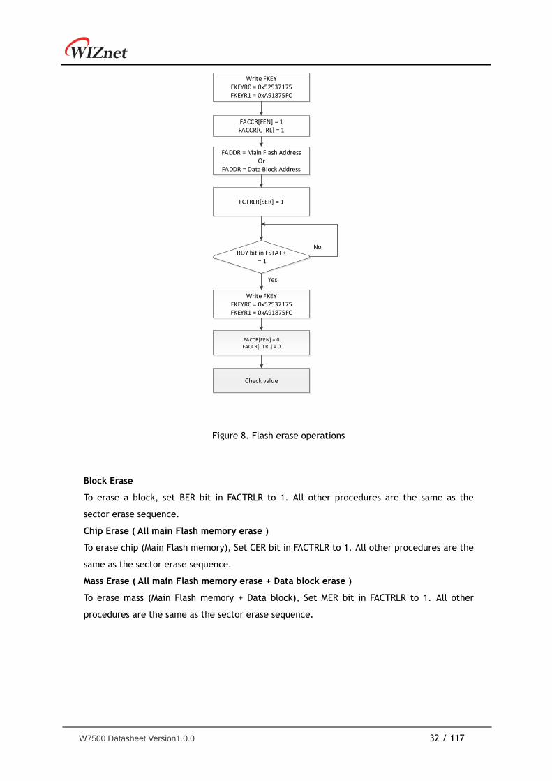
Flash erase operations 9.2.3
Sector Erase
Follow the procedure below to erase a sector:
1. Check that no Flash memory operation is ongoing by checking the RDY bit in the
FSTATR register.
2. Set KEY in FKEYR0/R1 for setting FACCR register.
3. Set FEN and CTRL bits in the FACCR register.
4. Write main Flash memory address to FADDA register to erase.
5. Set SER bit in FACTRLR to 1.
6. Wait until the RDY bit is 1 in the FSTATR register.
7. Set KEY in FKEYR0/R1 for clearing FACCR register.
8. Clear FEN and CTRL bits in the FACCR register
W7500 Datasheet Version1.0.0 32 / 117
Check value
Write FKEYFKEYR0 = 0x52537175FKEYR1 = 0xA91875FC
Write FKEYFKEYR0 = 0x52537175FKEYR1 = 0xA91875FC
FACCR[FEN] = 1FACCR[CTRL] = 1
FADDR = Main Flash AddressOr
FADDR = Data Block Address
FCTRLR[SER] = 1
RDY bit in FSTATR = 1
No
Yes
FACCR[FEN] = 0FACCR[CTRL] = 0
Figure 8. Flash erase operations
Block Erase
To erase a block, set BER bit in FACTRLR to 1. All other procedures are the same as the
sector erase sequence.
Chip Erase ( All main Flash memory erase )
To erase chip (Main Flash memory), Set CER bit in FACTRLR to 1. All other procedures are the
same as the sector erase sequence.
Mass Erase ( All main Flash memory erase + Data block erase )
To erase mass (Main Flash memory + Data block), Set MER bit in FACTRLR to 1. All other
procedures are the same as the sector erase sequence.
W7500 Datasheet Version1.0.0 33 / 117
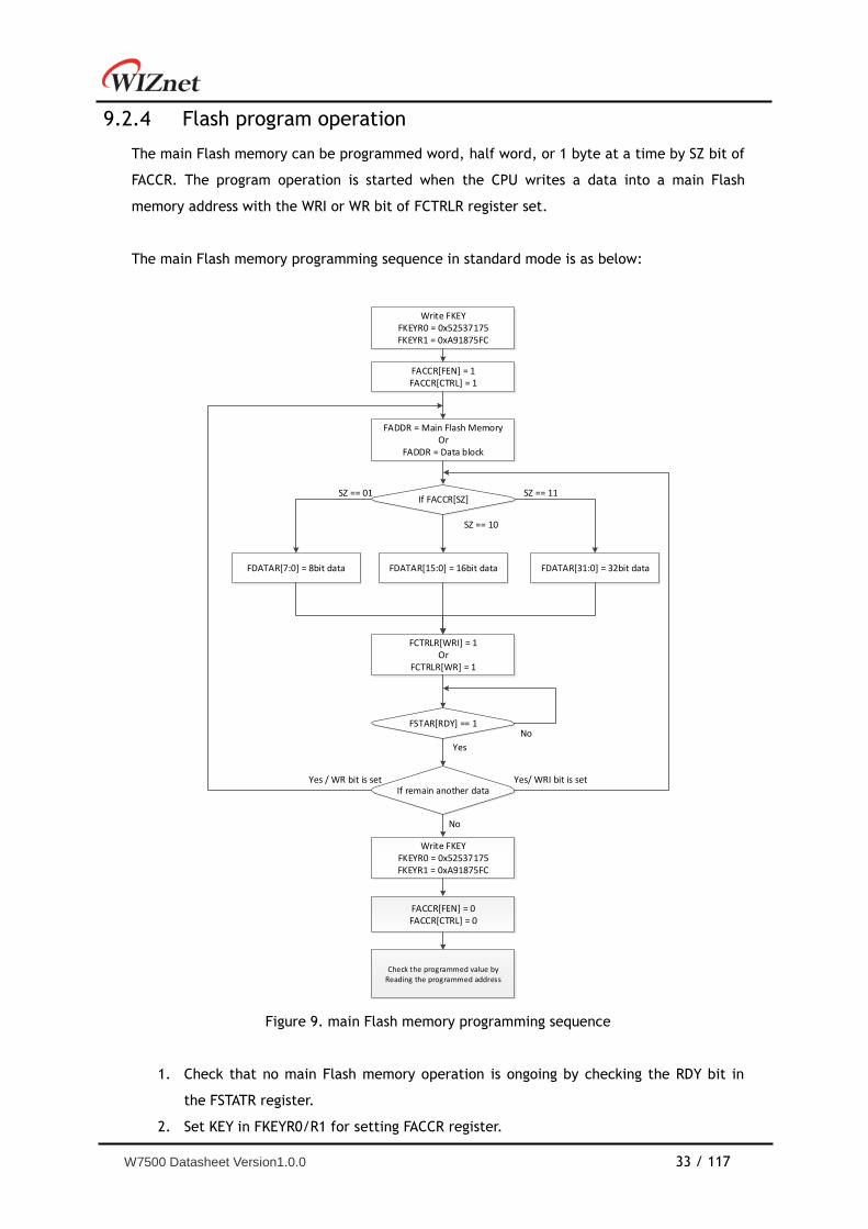
Flash program operation 9.2.4
The main Flash memory can be programmed word, half word, or 1 byte at a time by SZ bit of
FACCR. The program operation is started when the CPU writes a data into a main Flash
memory address with the WRI or WR bit of FCTRLR register set.
The main Flash memory programming sequence in standard mode is as below:
Write FKEYFKEYR0 = 0x52537175FKEYR1 = 0xA91875FC
FACCR[FEN] = 1FACCR[CTRL] = 1
FADDR = Main Flash MemoryOr
FADDR = Data block
FCTRLR[WRI] = 1Or
FCTRLR[WR] = 1
FSTAR[RDY] == 1No
Yes
If remain another dataYes/ WRI bit is setYes / WR bit is set
No
Check the programmed value by Reading the programmed address
FACCR[FEN] = 0FACCR[CTRL] = 0
Write FKEYFKEYR0 = 0x52537175FKEYR1 = 0xA91875FC
If FACCR[SZ]
FDATAR[7:0] = 8bit data FDATAR[15:0] = 16bit data FDATAR[31:0] = 32bit data
SZ == 01 SZ == 11
SZ == 10
Figure 9. main Flash memory programming sequence
1. Check that no main Flash memory operation is ongoing by checking the RDY bit in
the FSTATR register.
2. Set KEY in FKEYR0/R1 for setting FACCR register.
W7500 Datasheet Version1.0.0 34 / 117
3. Set FEN and CTRL bits in the FACCR register.
4. Write main Flash memory address or Data block address to FADDR register.
5. Write data to FDATAR register.
6. Set WRI or WR bit in FACTRLR to 1. If use WRI bit, don‟t need to set FADDR again due
to increase automatically by SZ bit in FACCR register.
7. Wait until the RDY bit is 1 in the FSTATR register.( it is set when the programming
operation has succeeded)
8. Set KEY in FKEYR0/R1 for clearing FACCR register.
9. Clear FEN and CTRL bits in the FACCR register
Memory protection 9.3
The user area of the Flash memory can be protected against read by untrusted code. The
blocks of the Flash memory can also be protected against unwanted write due to loss of
program counter contexts. The write-protection granularity is one block (4Kbyte).
Read protection 9.3.1
The read protection is activated by DRL bit and CRL bit in FLOCKR0 register.
DRL0 : read protection to Data0 area in Data block.
DRL1 : read protection to Data1 area.in Data block
CRL : read protection to main Flash memory
Write protection 9.3.2
The write protection is implemented with a granularity of one block. It is activated by
configuring the FLOCKR1 register or DWL bit, CABWL bit in FLOCKR0 register.
FLOCKR1 : write protection to main Flash memory with a granularity of one block.
DWL0 : write protection to Data0 area in Data block.
DWL1 : write protection to Data1 area in Data block.
CABWL : write protection to main Flash memory all block.
W7500 Datasheet Version1.0.0 35 / 117
10 Clock Reset generator (CRG)
10.1 Introduction
CRG is clock reset generator block for W7500 System. It provides every clock/reset for all
other block include CPU and peripherals. CRG includes PLL and POR.
10.2 Features
Reset 10.2.1
• Three types of reset – external reset, Power reset, system reset
• External reset is generated by low level on the RSTn pin (external reset)
• Power reset is generated by Power-on reset (POR)
• Power on reset is generated by POR
• System reset is generated when one of the following events occurs
Watchdog event
After remapping
Software reset (SYSRESETREQ bit in Cortex-M0. Refer to the Cortex-M0 technical
reference manual for more detail)
• Power reset sets all registers to their reset values.
• System reset sets all registers to their reset values except the CRG block registers and
remap register to protect remap value
Clock 10.2.2
Two clock sources can be used to drive the system clock.
External oscillator clock (8MHz ~ 24MHz) (OCLK)
Internal 8MHz RC oscillator clock (RCLK)
One additional clock source
32.768KHz low speed external crystal which derives the real time clock.
There is a PLL
One PLL is integrated
Input clock range is from 8MHz to 24MHz
Frequency can be generated by M/N/OD registers. (refer register description)
Bypass option enabled
There are many generated clocks for independent operating with system clock
System clock (FCLK)
ADC clock (ADCCLK)
SSP0, SSP1 clock (SSPCLK)
UART0, UART1 clock (UARTCLK)
W7500 Datasheet Version1.0.0 36 / 117
Two Timer clocks (TIMCLK0, TIMCLK1)
8ea PWM clocks (PWMCLK0 - PWMCLK7)
Real time clock (RTCCLK)
WDOG clock (WDOGCLK)
Random number generator clock (RNGCLK)
RNGCLK have only one source (pll output) and no prescaler
Some of the generated clocks turn off automatically when CPU enters sleep mode.
ADCCLK, RNGCLK
Generate two Hardware TCPIP Clocks (MII_RXC, MII_TXC) are from external PADs.
Hardware TCPIP Clocks can be gated by register control.
All clocks generated from CRG can be monitored.
10.3 Functional description
Figure 10 shows the CRG block diagram.
CRG
/1,2,4,8,16,32,64,128
/1,2,4,8,16,32,64,128
(8~24)MHzOSC
OSC_OUT
OSC_IN
8MHz RC
PLL
/1,2,4,8 FCLK
TIMCLK0/TIMCLK1
SSPCLK
PWMCLK0 - PWMCLK7
ADCCLK
MCLKFIN FOUT
RSTn
PORResetN(to Reset gen.)
SCLK
RCLK
OCLK
MCLK
RCLK
OCLK
/1,2,4,8
/1,2,4,8
/1,2,4,8,16,32,64,128
WDOGCLK
/1,2,4,8 UARTCLK
FCLK
OFF
/1,2,4,8,16,32,64,128..
/1,2,4,8,16,32,64,128FCLK
OFF
MCLK
OFF
RCLK
OCLK
MCLK
OFF
RCLK
OCLK
MCLK
OFF
RCLK
OCLK
MCLK
OFF
RCLK
OCLK
MCLK/1,2,4,8,16,32,64,128
Figure 10 CRG block diagram
External Oscillator Clock 10.3.1
External oscillator clock (OCLK) can be generated from two possible clock source
External crystal/ceramic resonator (8 to 24MHz external oscillator)
User external clock
Table 7 shows the two clock sources of external oscillator clock
Table 7 External oscillator clock sources
External clock Crystal/
W7500 Datasheet Version1.0.0 37 / 117
Ceramic resonators
Schematic
OSC_OUT
OSC_IN
8~24MHz
OSC_OUT
OSC_INExternalsource
NC
RC oscillator clock 10.3.2
RC oscillator clock (RCLK) signal is generated from an internal 8MHz RC oscillator.
RC oscillator has the advantage of providing a clock source at low cost (no external
components). However the RC oscillator is less accurate than the external crystal or ceramic
resonator.
Accuracy : 1% at TA= 25oC (User don‟t need to calibration)
PLL 10.3.3
The internal PLL can be used to multiply the External Oscillator Clock (OCLK) or RC Oscillator
Clock (RCLK). PLL input can be selected by register.
PLL output clock can be generated by following the equations below.
FOUT = FIN x M / N x 1 / OD
Where:
M = M[5] x 25 + M[4] x 24 + M[3] x 23 + M[2] x 22 + M[1] x 2 + M[0] x 1
N = N[5] x 25 + N[4] x 24 + N[3] x 23 + N[2] x 22 + N[1] x 2 + N[0] x 1
OD = 2 (2 x OD[1]) x 2 (1 x OD[0])
Generated clock 10.3.4
Each generated clock source can be selected among 3 clock source as independent by each
clock source select register.
PLL output clock (MCLK)
Internal 8MHz RC oscillator clock (RCLK)
External oscillator clock (8MHz ~ 24MHz) (OCLK)
Each generated clock has own prescaler which can be selected individually by each prescale
value register.
FCLK, ADCCLK, SSPCLK, UARTCLK : 1/1, 1/2, 1/4, 1/8
TIMCLK0, TIMCLK1, PWMCLK0 – PWMCLK7, RTCCLK, WDOGCLK : 1/1, 1/2, 1/4,
1/8, 1/16, 1/32, 1/64, 1/128
W7500 Datasheet Version1.0.0 38 / 117
11 Random number generator (RNG)
Introduction 11.1
RNG is a 32bit random number generator. RNG generates power on random number when
power on reset. RNG can run/stop by software. RNG seed value and polynomial of RNG can
be modified by software.
Features 11.2
• 32bit pseudo random number generator
• Formula of pseudo random number generator (polynomial) can be modified.
• Seed value of random generator can be modified.
• Support power on reset random value
• Random value can be obtained by control start/stop by software.
Functional description 11.3
Figure 11 shows the RNG block diagram.
PCLK
RU
N
RN
GCLK
PLL_L
OCK
0 1 n-4 n-3 n-2 n-1
0 1 2 n-3 n-2 n-1
0 1 2 n-3 n-2 n-1
Polynomial Registers
ShiftRegisters
SeedRegisters
Controller(Registers)
CLKSEL
MO
DE
SEED
[31:0
]
PO
LY[3
1:0
]
CLK
RSTn
RN
[31;0
]
RSTn
AD
CCLK
APB IF
n = 32
Figure 11. Random Number Generator block diagram
W7500 Datasheet Version1.0.0 39 / 117
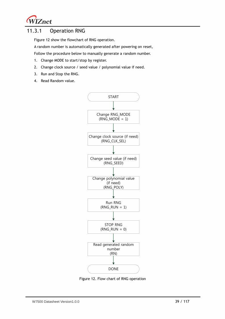
Operation RNG 11.3.1
Figure 12 show the flowchart of RNG operation.
A random number is automatically generated after powering on reset,
Follow the procedure below to manually generate a random number.
1. Change MODE to start/stop by register.
2. Change clock source / seed value / polynomial value if need.
3. Run and Stop the RNG.
4. Read Random value.
START
Change clock source (if need)(RNG_CLK_SEL)
Change seed value (if need)(RNG_SEED)
Change polynomial value (if need)
(RNG_POLY)
Run RNG(RNG_RUN = 1)
STOP RNG(RNG_RUN = 0)
DONE
Change RNG_MODE(RNG_MODE = 1)
Read generated random number
(RN)
Figure 12. Flow chart of RNG operation
W7500 Datasheet Version1.0.0 40 / 117
12 Alternate Function Controller (AFC)
Introduction 12.1
Each functional PADs have several functions.
Users can select a function in Alternate Function Controller block.
Features 12.2
Each functional pad has 2 ~ 4 functions.
Pads can be selected by each registers individually.
Each pad can be used as external interrupt source.
Functional description 12.3
Table 8 shows the function table of each functional pad.
Table 8 functional description table
function selection register value
00 (reset value) 01 10 11
PAD
NAME
PIN
NUM
Normal Function 2nd Function 3rd Function 4th Function
PA_00 29 GPIOA_0 GPIOA_0 PWM6/CAP6
PA_01 30 GPIOA_1 GPIOA_1 PWM7/CAP7
PA_02 31 GPIOA_2 GPIOA_2 CLKOUT
PA_03 49 SWCLK GPIOA_3
PA_04 50 SWDIO GPIOA_4
PA_05 33 SSEL0 GPIOA_5 SCL1 PWM2/CAP2
PA_06 34 SCLK0 GPIOA_6 SDA1 PWM3/CAP3
PA_07 35 MISO0 GPIOA_7 U_CTS1 PWM4/CAP4
PA_08 36 MOSI0 GPIOA_8 U_RTS1 PWM5/CAP5
PA_09 37 SCL0 GPIOA_9 U_TXD1 PWM6/CAP6
PA_10 38 SDA0 GPIOA_10 U_RXD1 PWM7/CAP7
PA_11 40 U_CTS0 GPIOA_11 SSEL1
PA_12 41 U_RTS0 GPIOA_12 SCLK1
PA_13 42 U_TXD0 GPIOA_13 MISO1
PA_14 43 U_RXD0 GPIOA_14 MOSI1
PA_15 44 GPIOA_15 GPIOA_15
PB_00 45 SSEL1 GPIOB_0 U_CTS0
PB_01 46 SCLK1 GPIOB_1 U_RTS0
PB_02 47 MISO1 GPIOB_2 U_TXD0
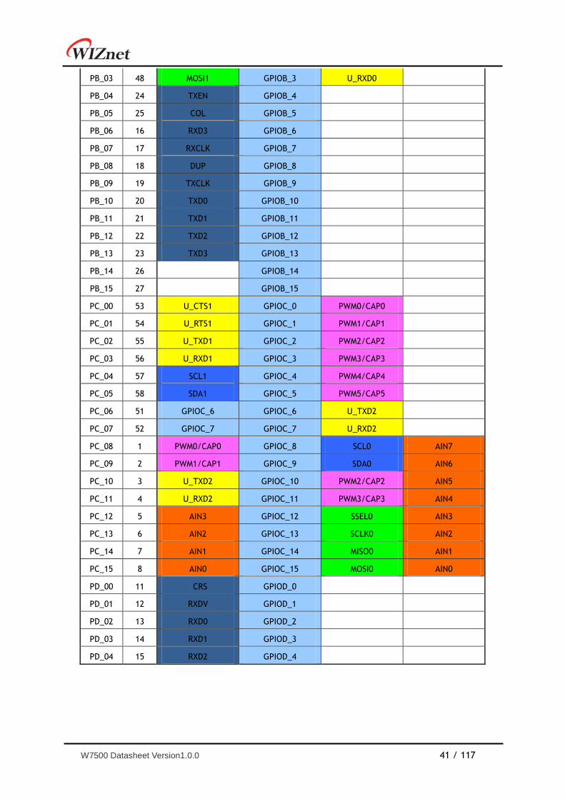
W7500 Datasheet Version1.0.0 41 / 117
PB_03 48 MOSI1 GPIOB_3 U_RXD0
PB_04 24 TXEN GPIOB_4
PB_05 25 COL GPIOB_5
PB_06 16 RXD3 GPIOB_6
PB_07 17 RXCLK GPIOB_7
PB_08 18 DUP GPIOB_8
PB_09 19 TXCLK GPIOB_9
PB_10 20 TXD0 GPIOB_10
PB_11 21 TXD1 GPIOB_11
PB_12 22 TXD2 GPIOB_12
PB_13 23 TXD3 GPIOB_13
PB_14 26 GPIOB_14
PB_15 27 GPIOB_15
PC_00 53 U_CTS1 GPIOC_0 PWM0/CAP0
PC_01 54 U_RTS1 GPIOC_1 PWM1/CAP1
PC_02 55 U_TXD1 GPIOC_2 PWM2/CAP2
PC_03 56 U_RXD1 GPIOC_3 PWM3/CAP3
PC_04 57 SCL1 GPIOC_4 PWM4/CAP4
PC_05 58 SDA1 GPIOC_5 PWM5/CAP5
PC_06 51 GPIOC_6 GPIOC_6 U_TXD2
PC_07 52 GPIOC_7 GPIOC_7 U_RXD2
PC_08 1 PWM0/CAP0 GPIOC_8 SCL0 AIN7
PC_09 2 PWM1/CAP1 GPIOC_9 SDA0 AIN6
PC_10 3 U_TXD2 GPIOC_10 PWM2/CAP2 AIN5
PC_11 4 U_RXD2 GPIOC_11 PWM3/CAP3 AIN4
PC_12 5 AIN3 GPIOC_12 SSEL0 AIN3
PC_13 6 AIN2 GPIOC_13 SCLK0 AIN2
PC_14 7 AIN1 GPIOC_14 MISO0 AIN1
PC_15 8 AIN0 GPIOC_15 MOSI0 AIN0
PD_00 11 CRS GPIOD_0
PD_01 12 RXDV GPIOD_1
PD_02 13 RXD0 GPIOD_2
PD_03 14 RXD1 GPIOD_3
PD_04 15 RXD2 GPIOD_4
W7500 Datasheet Version1.0.0 42 / 117
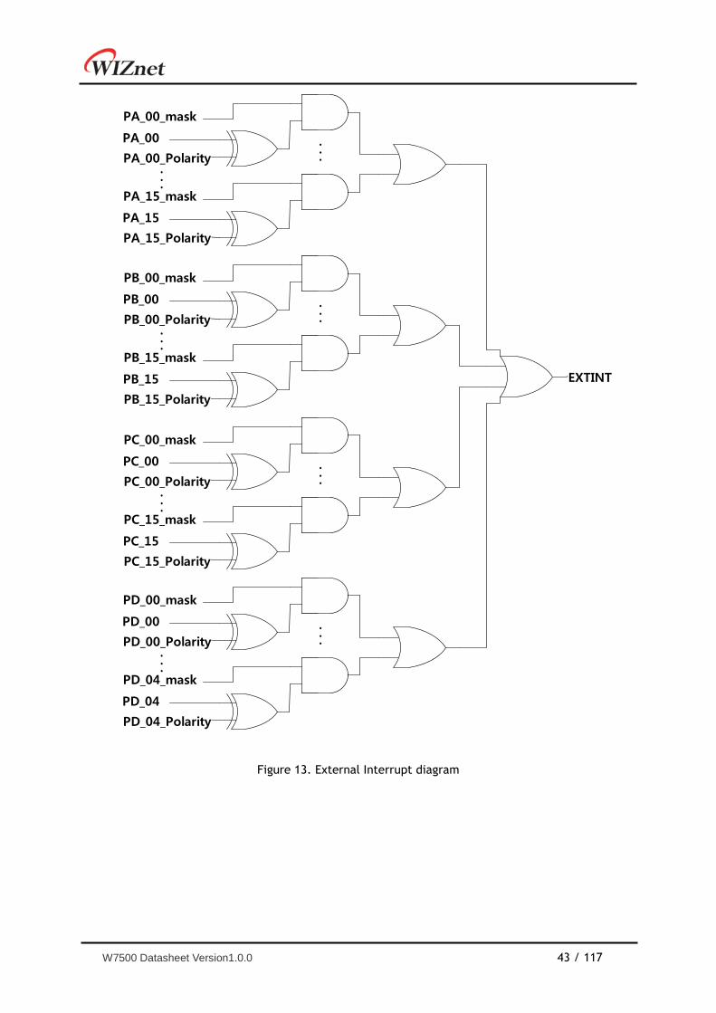
13 External Interrupt (EXTI)
Introduction 13.1
Each functional pads are connected to the external interrupt(EXTINT) source.
Features 13.2
• All functional pads can be used as an external interrupt source regardless of any set of
pad function.
• External Interrupt controller has the following functions and can be controlled by
registers.
Interrupt mask (enable or disable, default : disable)
Interrupt polarity (rising or falling, default : rising)
Functional description 13.3
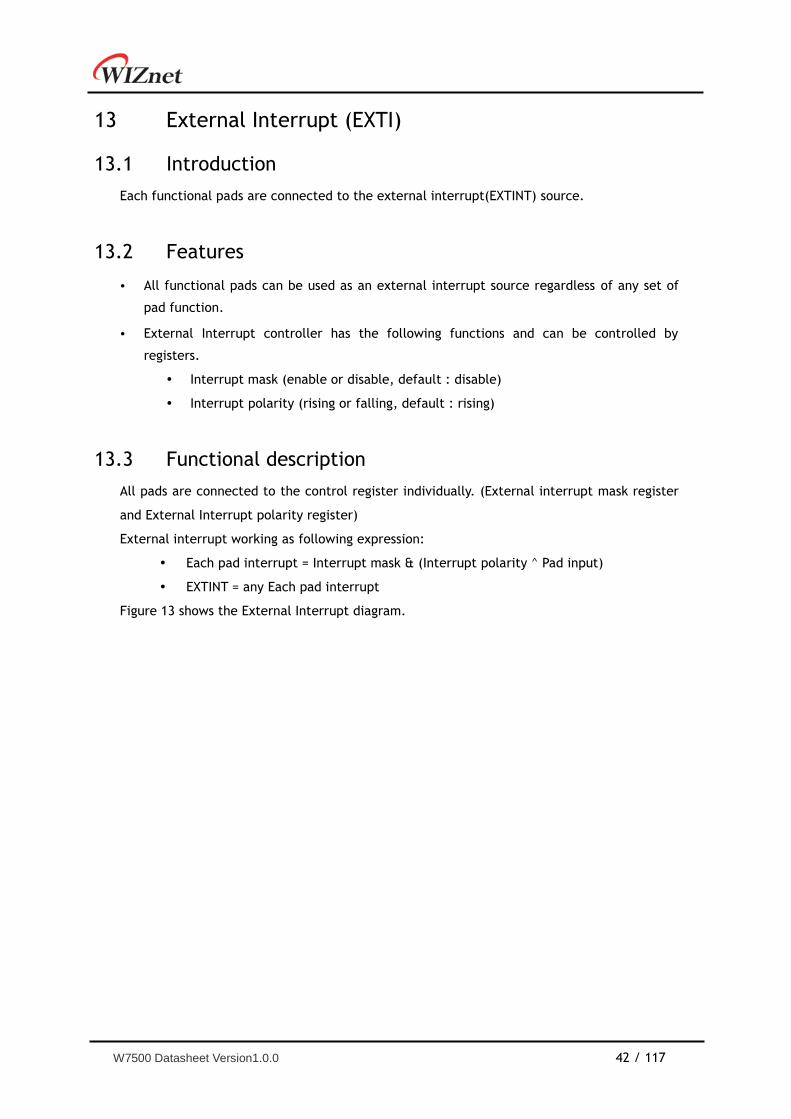
All pads are connected to the control register individually. (External interrupt mask register
and External Interrupt polarity register)
External interrupt working as following expression:
Each pad interrupt = Interrupt mask & (Interrupt polarity ^ Pad input)
EXTINT = any Each pad interrupt
Figure 13 shows the External Interrupt diagram.
W7500 Datasheet Version1.0.0 43 / 117
PA_00_Polarity
PA_00_mask
PA_00
EXTINT
. . .
. . .
PA_15_Polarity
PA_15_mask
PA_15
PB_00_Polarity
PB_00_mask
PB_00
. . .
. . .PB_15_Polarity
PB_15_mask
PB_15
PC_00_Polarity
PC_00_mask
PC_00
. . .
. . .
PC_15_Polarity
PC_15_mask
PC_15
PD_00_Polarity
PD_00_mask
PD_00
. . .
. . .
PD_04_Polarity
PD_04_mask
PD_04
Figure 13. External Interrupt diagram
W7500 Datasheet Version1.0.0 44 / 117
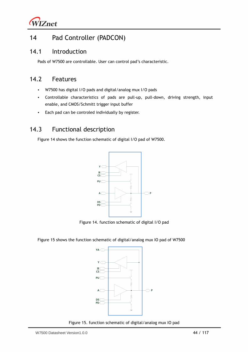
14 Pad Controller (PADCON)
Introduction 14.1
Pads of W7500 are controllable. User can control pad‟s characteristic.
Features 14.2
• W7500 has digital I/O pads and digital/analog mux I/O pads
• Controllable characteristics of pads are pull-up, pull-down, driving strength, input
enable, and CMOS/Schmitt trigger input buffer
• Each pad can be controled individually by register.
Functional description 14.3
Figure 14 shows the function schematic of digital I/O pad of W7500.
P
Y
CS
PU
PDDS
A
IE
Figure 14. function schematic of digital I/O pad
Figure 15 shows the function schematic of digital/analog mux IO pad of W7500
P
YA
Y
CS
PU
PDDS
A
IE
Figure 15. function schematic of digital/analog mux IO pad
W7500 Datasheet Version1.0.0 45 / 117
Initials of Pad diagram is same as below.
P - PAD
YA – Analog Input (connect to ADC input)
Y – Digital Input
IE – Input buffer enable
CS – CMOS/Schmitt trigger input buffer select
PU – Pull-up enable
A – Digital Output
DS – Driving strength select
PD – Pull-down enable
User can set pad condition with IE, CS, PU/PD, DS by register.
And pads are can be controlled individually.
15 General-purpose I/Os(GPIO)
Introduction 15.1
The GPIO(General-Purpose I/O Port) is composed of four physical GPIO blocks, each
corresponding to an individual GPIO port(PORT A, PORT B, PORT C, PORT D). The GPIO
supports up to 53 programmable input/output pins, depending on the peripherals being used.
Features 15.2
• The GPIO peripheral consists the following features.
GPIO_DATAOUT can SET/CLEAR by the SET register and CLEAR register. (1 for set and
0 for clear)
Condition A Y P
Input buffer enable
(IE = 1)
Output mode OUT OUT OUT
Input mode No use IN IN
Input buffer disable
(IE = 0)
Output mode OUT Low (0) OUT
Input mode No use IN IN
Condition Rise/Fall Time (nSec) Propagation Delay (nSec)
Driving Strength Capacitance
loading Min Max Min Max
High
(DS = 1)
25pF 4 18 7 27
100pF 11 53 11 44
Low
(DS = 0)
25pF 1 8 4 16
100pF 4 23 7 24
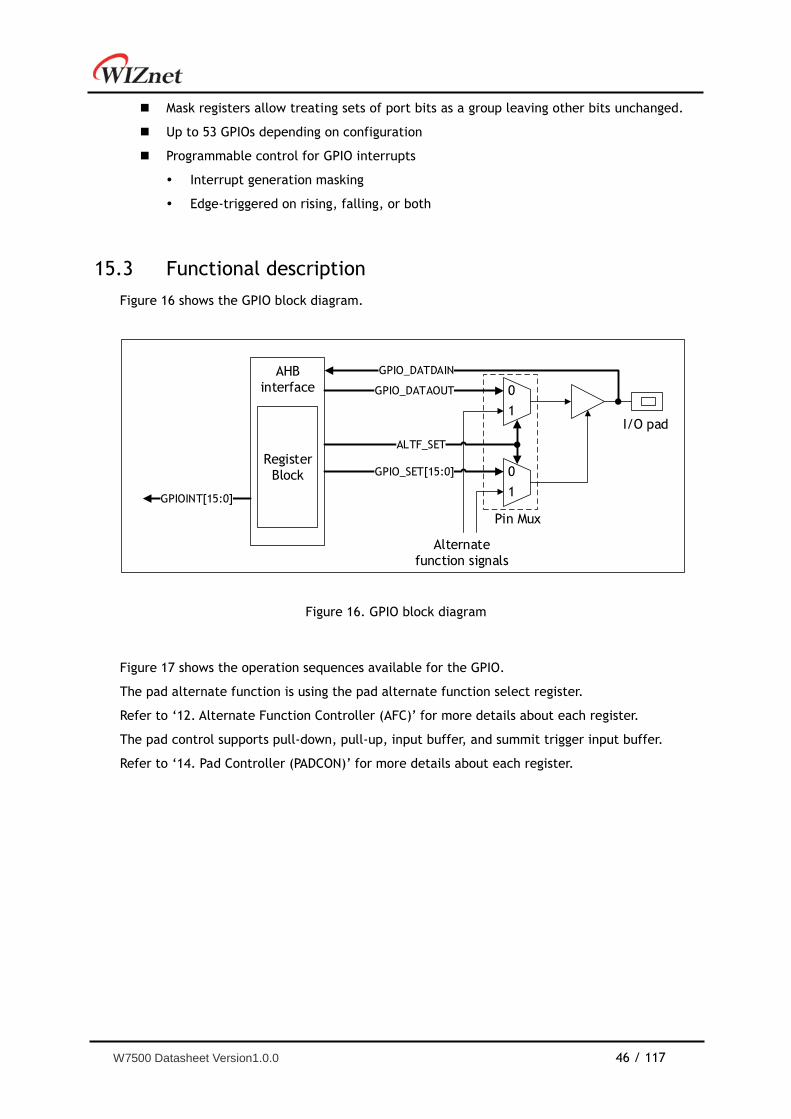
W7500 Datasheet Version1.0.0 46 / 117
Mask registers allow treating sets of port bits as a group leaving other bits unchanged.
Up to 53 GPIOs depending on configuration
Programmable control for GPIO interrupts
Interrupt generation masking
Edge-triggered on rising, falling, or both
Functional description 15.3
Figure 16 shows the GPIO block diagram.
AHB
interface
Register
Block
0
1
0
1
GPIO_DATAOUT
GPIO_DATDAIN
GPIO_SET[15:0]
ALTF_SET
GPIOINT[15:0]
Alternate
function signals
I/O pad
Pin Mux
Figure 16. GPIO block diagram
Figure 17 shows the operation sequences available for the GPIO.
The pad alternate function is using the pad alternate function select register.
Refer to „12. Alternate Function Controller (AFC)‟ for more details about each register.
The pad control supports pull-down, pull-up, input buffer, and summit trigger input buffer.
Refer to „14. Pad Controller (PADCON)‟ for more details about each register.
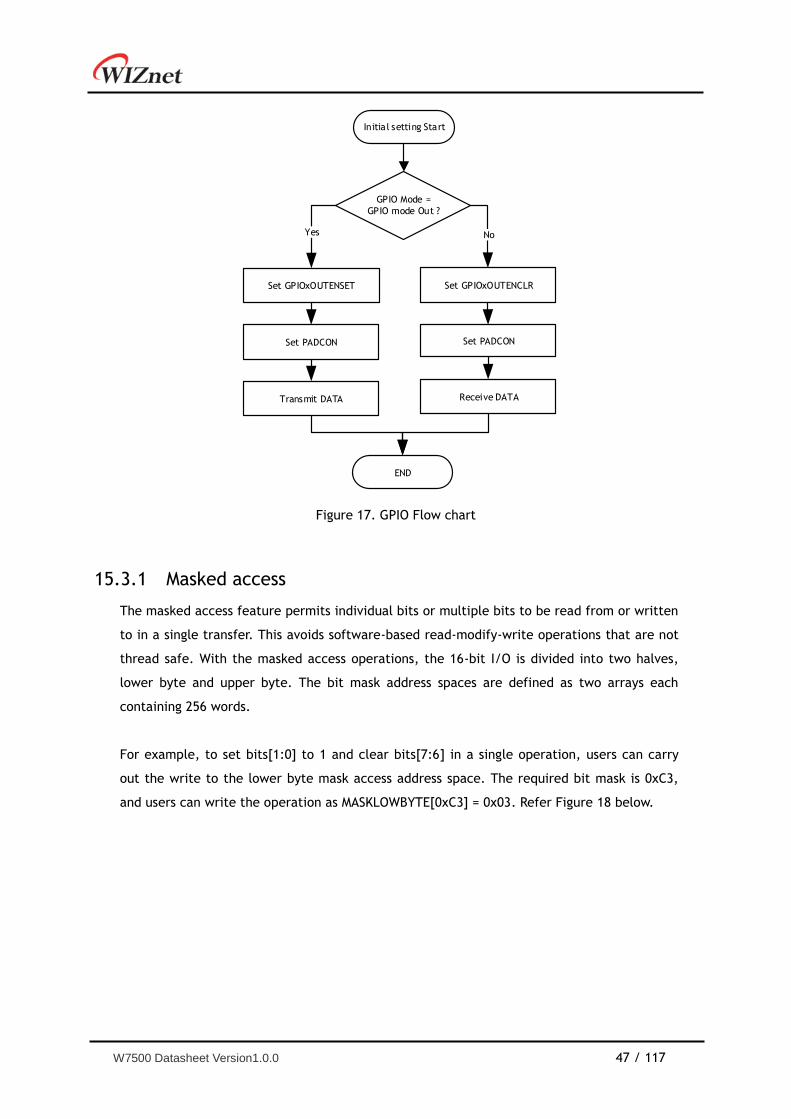
W7500 Datasheet Version1.0.0 47 / 117
Initial setting Start
GPIO Mode =
GPIO mode Out ?
Yes
Set GPIOxOUTENSET Set GPIOxOUTENCLR
No
Set PADCON Set PADCON
Transmit DATA Receive DATA
END
Figure 17. GPIO Flow chart
Masked access 15.3.1
The masked access feature permits individual bits or multiple bits to be read from or written
to in a single transfer. This avoids software-based read-modify-write operations that are not
thread safe. With the masked access operations, the 16-bit I/O is divided into two halves,
lower byte and upper byte. The bit mask address spaces are defined as two arrays each
containing 256 words.
For example, to set bits[1:0] to 1 and clear bits[7:6] in a single operation, users can carry
out the write to the lower byte mask access address space. The required bit mask is 0xC3,
and users can write the operation as MASKLOWBYTE[0xC3] = 0x03. Refer Figure 18 below.
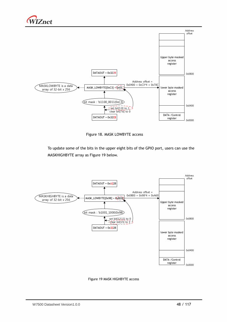
W7500 Datasheet Version1.0.0 48 / 117
Upper byte masked
access
register
lower byte masked
access
register
0x0800
0x0400
DATA /Control
register0x0000
Addressoffset
DATAOUT = 0x32E8
set bit[1:0] to 1clear bit[7:6] to 0
bit mask : 'b1100_0011(0xC3)
MASK_LOWBYTE[0xC3] = 0x03
Address offset = 0x0400 + 0xC3*4 = 0x70C
DATAOUT = 0x322B
MASKLOWBYTE is a dataarray of 32-bit x 256
Figure 18. MASK LOWBYTE access
To update some of the bits in the upper eight bits of the GPIO port, users can use the
MASKHIGHBYTE array as Figure 19 below.
Upper byte masked
access
register
lower byte masked
access
register
0x0800
0x0400
DATA /Control
register0x0000
Addressoffset
DATAOUT = 0x322B
set bit[12:11] to 0clear bit[15] to 1
bit mask : 'b1001_1000(0x98)
MASK_LOWBYTE[0x98] = 0x8000
Address offset = 0x0800 + 0x98*4 = 0xA60
DATAOUT = 0xA22B
MASKHIGHBYTE is a dataarray of 32-bit x 256
Figure 19 MASK HIGHBYTE access
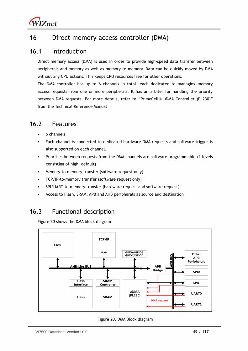
W7500 Datasheet Version1.0.0 49 / 117
16 Direct memory access controller (DMA)
Introduction 16.1
Direct memory access (DMA) is used in order to provide high-speed data transfer between
peripherals and memory as well as memory to memory. Data can be quickly moved by DMA
without any CPU actions. This keeps CPU resources free for other operations.
The DMA controller has up to 6 channels in total, each dedicated to managing memory
access requests from one or more peripherals. It has an arbiter for handling the priority
between DMA requests. For more details, refer to “PrimeCell® μDMA Controller (PL230)”
from the Technical Reference Manual
Features 16.2
• 6 channels
• Each channel is connected to dedicated hardware DMA requests and software trigger is
also supported on each channel.
• Priorities between requests from the DMA channels are software programmable (2 levels
consisting of high, default)
• Memory-to-memory transfer (software request only)
• TCP/IP-to-memory transfer (software request only)
• SPI/UART-to-memory transfer (hardware request and software request)
• Access to Flash, SRAM, APB and AHB peripherals as source and destination
Functional description 16.3
Figure 20 shows the DMA block diagram.
GPIO x 16
CM0
AHB-Lite BUS
Flash
FlashInterface
SRAMController
SRAM
uDMA(PL230)
TCP/IP
GPIOA/GPIOBGPIOC/GPIOD
SRAM
APB B
US Other
APBPeripherals
APBBridge
UART0
SPI0
SPI1
UART1
DMA request
Figure 20. DMA Block diagram
W7500 Datasheet Version1.0.0 50 / 117
DMA request mapping 16.3.1
The hardware requests from the peripherals (UART0, UART1, SSP0, SSP1) are simply
connected to the DMA. Refer to Table 9 which lists the DMA requests for each channel.
Table 9 Summary of the DMA requests for each channel
Channel 1 Channel 2 Channel 3 Channel 4 Channel 5 Channel 6
Hardware
Request
SSP0_TX
SSP0_RX
SSP1_TX
SSP1_RX
UART0_TX
UART0_RX
UART1_TX
UART1_RX NONE NONE
Software
Request(1) Support Support Support Support Support Support
1. Software request is the only way to use DMA for memory-to-memory or TCP/IP-to-
memory.
DMA arbitration 16.3.2
The controller can be configured to perform arbitration during a DMA cycle before and after
a programmable number of transfers. This reduces the latency for servicing a higher priority
channel.
The controller uses four bits in the channel control data structure that configures how many
AHB bus transfers occur before the controller re-arbitrates. These bits are known as the
R_power bits because the value R is raised to the power of two and this determines the
arbitration rate. For example, if R = 4, then the arbitration rate is 24, which means the
controller arbitrates every 16 DMA transfers.
Remark: Do not assign a low-priority channel with a large R_power value because this
prevents the controller from servicing high-priority requests until it re-arbitrates.
When N > 2R and is not an integer multiple of 2R, then the controller always performs
sequences of 2Rtransfers until N < 2R remain to be transferred. The controller performs the
remaining N transfers at the end of the DMA cycle.
DMA cycle types 16.3.3
The cycle_ctrl bits in the channel control data structure contril how the DMA controller
performs a cycle.
The controller uses four cycle types described in this manual:
Invalid
W7500 Datasheet Version1.0.0 51 / 117
Basic
Auto-request
Ping-pong
See ARM micro DMA (PL230) documentation for additional cycle types.
For all cycle types, the controller arbitrates after 2R DMA transfers. If a low-priority channel
is set to a large 2R value then it prevents all other channels from performing a DMA transfer
until the low-priority DMA transfer completes. Therefore, the user must be cautious when
setting the R_power bit in the channel_cfg data structure so that the latency for high-priority
channels is not significantly increased.
16.3.3.1 Invalid cycle
After the controller completes a DMA cycle, it sets the cycle type to invalid to prevent it
from repeating the same DMA cycle.
16.3.3.2 Basic cycle
In this mode, the controller can be configured to use either the primary or the alternate
channel control data structure. After the channel is enabled and the controller receives a
request for this channel, the flow for basic cycle is as below:
1. The controller performs 2R transfers.
If the number of transfers remaining is zero the flow continues at step 3.
2. The controller arbitrates:
- If a higher-priority channel is requesting service, then the controller services that
channel.
- If the peripheral or software signals a request to the controller, then it continues at
step 1.
3. The controller sets dma_done[c] signal for this channel HIGH for one system clock cycle.
This indicates to the host processor that the DMA cycle is complete.
16.3.3.3 Auto-request cycle
When the controller operates in this mode, it is only necessary to receive a single request to
enable the controller to complete the entire DMA cycle. This enables a large data transfer to
occur, without significantly increasing the latency for servicing higher priority requests or
requiring multiple requests from the processor or peripheral.
W7500 Datasheet Version1.0.0 52 / 117
The auto-request cycle is typically used for memory-to-memory requests. In this case,
software generates the starting request for the 2R transfers after setting up the DMA control
data structure.
In this mode, the controller can be configured to use either the primary or the alternate
channel control data structure. After the channel is enabled and the controller receives a
request for this channel, the flow for the auto-request cycle is as below:
1. The controller performs 2R transfers. If the number of transfers remaining
is zero the flow continues at step 3.
2. The controller arbitrates if there are any transfers remaining after 2R
transfers. If the current channel c has the highest priority, the cycle
continues at step 1.
3. The controller sets dma_done[c] signal for this channel HIGH for one system
clock cycle. This indicates to the host processor that the DMA cycle is
complete.
16.3.3.4 Ping-pong cycle
In this mode, the controller performs a DMA cycle using one of the data structures and then
performs a DMA cycle using the other data structure. The controller continues to switch
between primary and alternate structures until it either reads a data structure that is invalid,
or until the user reprograms the cycle_type to basic, or until the host processor disables the
channel.
In ping-pong mode, the user can program or reprogram one of the two channel data
structures (primary or alternate) while using the other channel data structure for the active
transfer. When a transfer is done, the next transfer can be started immediately using the
prepared channel data structure – provided that a higher priority channel does not require
servicing. If the user does not reprogram the channel control data structure not in use for a
transfer, the cycle type remains invalid (which is the value at the end of the last transfer
using that structure) and the ping-pong cycle completes.
The ping-pong cycle can be used for transfers to or from peripherals or for memory-to-
memory transfers.
W7500 Datasheet Version1.0.0 53 / 117
Figure 21. DMA ping pong cycle
W7500 Datasheet Version1.0.0 54 / 117
17 Analog-to-digital converter (ADC)
Introduction 17.1
ADC is a 12bit analog-to-digital converter. It has up to 9 multiplexed channels allowing it to
measure signals from 8 externals and 1 internal source.
ADC of various channels can be performed in single mode. The result of the ADC is stored in
12 bit register.
Features 17.2
• 12bit configuration resolution
• Conversion time : Max 10MHz (Sampling time can be programmable)
8 channel for external analog inputs
CH0 : PC_15
CH1 : PC_14
CH2 : PC_13
CH3 : PC_12
CH4 : PC_11
CH5 : PC_10
CH6 : PC_09
CH7 : PC_08
1 channel for internal LDO(1.5v) voltage.
CH15 : Internal voltage
• Start of conversion can be initiated by software.
• Convert selected inputs once per trigger.
• Interrupt generation at the end of conversion.
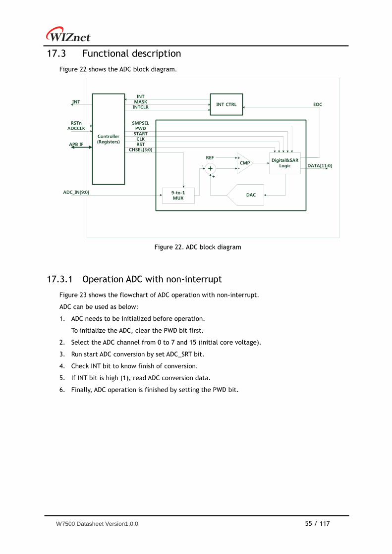
W7500 Datasheet Version1.0.0 55 / 117
Functional description 17.3
Figure 22 shows the ADC block diagram.
9-to-1MUX
Digital&SARLogic+
CMP
DAC
+
-
+
-
REF
Controller(Registers)
SMPSELPWD
CHSEL[3:0]
STARTCLKRST
DATA[11:0]
EOC
RSTnADCCLK
APB IF
ADC_IN[9:0]
MASKINT
INTINT CTRL
INTCLR
Figure 22. ADC block diagram
Operation ADC with non-interrupt 17.3.1
Figure 23 shows the flowchart of ADC operation with non-interrupt.
ADC can be used as below:
1. ADC needs to be initialized before operation.
To initialize the ADC, clear the PWD bit first.
2. Select the ADC channel from 0 to 7 and 15 (initial core voltage).
3. Run start ADC conversion by set ADC_SRT bit.
4. Check INT bit to know finish of conversion.
5. If INT bit is high (1), read ADC conversion data.
6. Finally, ADC operation is finished by setting the PWD bit.
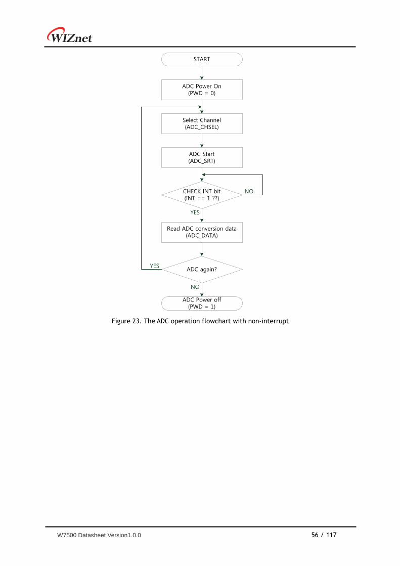
W7500 Datasheet Version1.0.0 56 / 117
START
ADC Power On(PWD = 0)
Select Channel(ADC_CHSEL)
CHECK INT bit(INT == 1 ??)
Read ADC conversion data(ADC_DATA)
ADC Start(ADC_SRT)
YES
NO
ADC again?
ADC Power off(PWD = 1)
NO
YES
Figure 23. The ADC operation flowchart with non-interrupt
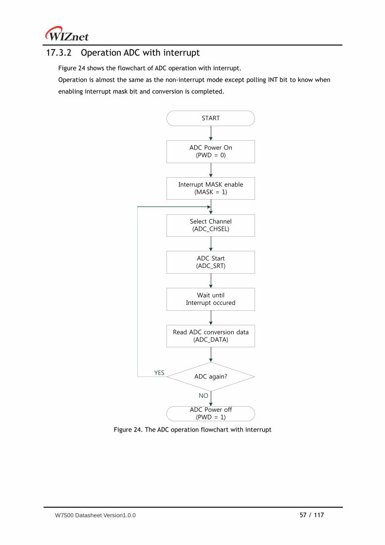
W7500 Datasheet Version1.0.0 57 / 117
Operation ADC with interrupt 17.3.2
Figure 24 shows the flowchart of ADC operation with interrupt.
Operation is almost the same as the non-interrupt mode except polling INT bit to know when
enabling interrupt mask bit and conversion is completed.
START
ADC Power On(PWD = 0)
Interrupt MASK enable(MASK = 1)
Select Channel(ADC_CHSEL)
ADC Start(ADC_SRT)
Wait untilInterrupt occured
Read ADC conversion data(ADC_DATA)
ADC again?
ADC Power off(PWD = 1)
NO
YES
Figure 24. The ADC operation flowchart with interrupt
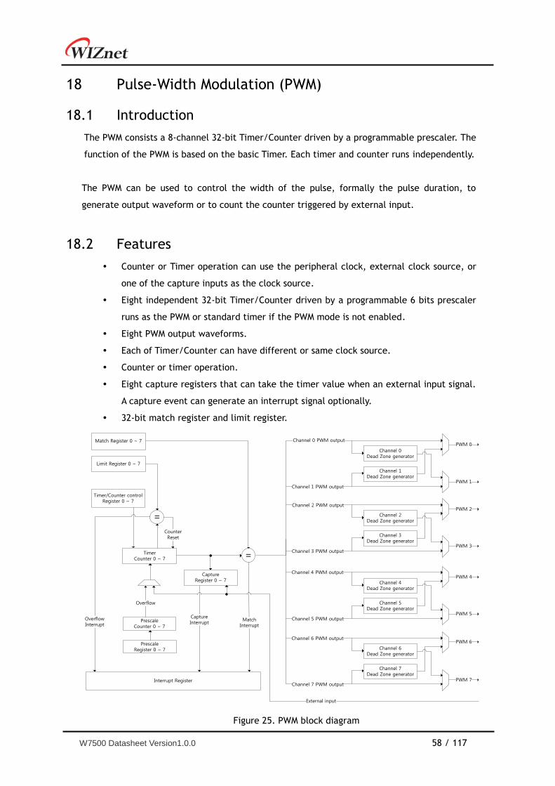
W7500 Datasheet Version1.0.0 58 / 117
18 Pulse-Width Modulation (PWM)
Introduction 18.1
The PWM consists a 8-channel 32-bit Timer/Counter driven by a programmable prescaler. The
function of the PWM is based on the basic Timer. Each timer and counter runs independently.
The PWM can be used to control the width of the pulse, formally the pulse duration, to
generate output waveform or to count the counter triggered by external input.
Features 18.2
Counter or Timer operation can use the peripheral clock, external clock source, or
one of the capture inputs as the clock source.
Eight independent 32-bit Timer/Counter driven by a programmable 6 bits prescaler
runs as the PWM or standard timer if the PWM mode is not enabled.
Eight PWM output waveforms.
Each of Timer/Counter can have different or same clock source.
Counter or timer operation.
Eight capture registers that can take the timer value when an external input signal.
A capture event can generate an interrupt signal optionally.
32-bit match register and limit register.
Figure 25. PWM block diagram
TimerCounter 0 ~ 7
PrescaleRegister 0 ~ 7
PrescaleCounter 0 ~ 7
=
MatchInterrupt
Match Register 0 ~ 7
Timer/Counter controlRegister 0 ~ 7
Limit Register 0 ~ 7
CaptureRegister 0 ~ 7
=
CounterReset
OverflowInterrupt
Overflow
CaptureInterrupt
Channel 0 PWM output
Channel 0Dead Zone generator
Channel 1 PWM output
Channel 1Dead Zone generator
External input
PWM 0
PWM 1
Channel 2 PWM output
Channel 2Dead Zone generator
Channel 3 PWM output
Channel 3Dead Zone generator
PWM 2
PWM 3
Channel 4 PWM output
Channel 4Dead Zone generator
Channel 5 PWM output
Channel 5Dead Zone generator
Channel 6 PWM output
Channel 6Dead Zone generator
Channel 7 PWM output
Channel 7Dead Zone generator
Interrupt Register
PWM 4
PWM 5
PWM 6
PWM 7
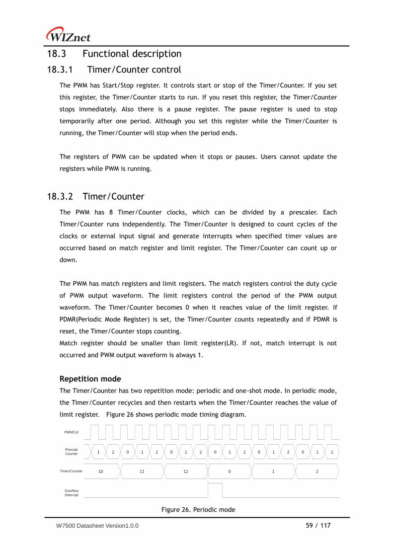
W7500 Datasheet Version1.0.0 59 / 117
Functional description 18.3
Timer/Counter control 18.3.1
The PWM has Start/Stop register. It controls start or stop of the Timer/Counter. If you set
this register, the Timer/Counter starts to run. If you reset this register, the Timer/Counter
stops immediately. Also there is a pause register. The pause register is used to stop
temporarily after one period. Although you set this register while the Timer/Counter is
running, the Timer/Counter will stop when the period ends.
The registers of PWM can be updated when it stops or pauses. Users cannot update the
registers while PWM is running.
Timer/Counter 18.3.2
The PWM has 8 Timer/Counter clocks, which can be divided by a prescaler. Each
Timer/Counter runs independently. The Timer/Counter is designed to count cycles of the
clocks or external input signal and generate interrupts when specified timer values are
occurred based on match register and limit register. The Timer/Counter can count up or
down.
The PWM has match registers and limit registers. The match registers control the duty cycle
of PWM output waveform. The limit registers control the period of the PWM output
waveform. The Timer/Counter becomes 0 when it reaches value of the limit register. If
PDMR(Periodic Mode Register) is set, the Timer/Counter counts repeatedly and if PDMR is
reset, the Timer/Counter stops counting.
Match register should be smaller than limit register(LR). If not, match interrupt is not
occurred and PWM output waveform is always 1.
Repetition mode
The Timer/Counter has two repetition mode: periodic and one-shot mode. In periodic mode,
the Timer/Counter recycles and then restarts when the Timer/Counter reaches the value of
limit register. Figure 26 shows periodic mode timing diagram.
Figure 26. Periodic mode
PWMCLK
Timer/Counter 11 12 0 1 2
Overflow Interrupt
10
PrescaleCounter 0 1 2 0 1 2 0 1 2 0 1 2 0 1 21 2
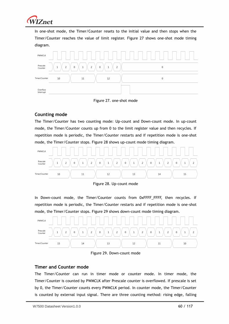
W7500 Datasheet Version1.0.0 60 / 117
In one-shot mode, the Timer/Counter resets to the initial value and then stops when the
Timer/Counter reaches the value of limit register. Figure 27 shows one-shot mode timing
diagram.
Figure 27. one-shot mode
Counting mode
The Timer/Counter has two counting mode: Up-count and Down-count mode. In up-count
mode, the Timer/Counter counts up from 0 to the limit register value and then recycles. If
repetition mode is periodic, the Timer/Counter restarts and if repetition mode is one-shot
mode, the Timer/Counter stops. Figure 28 shows up-count mode timing diagram.
Figure 28. Up-count mode
In Down-count mode, the Timer/Counter counts from 0xFFFF_FFFF, then recycles. If
repetition mode is periodic, the Timer/Counter restarts and if repetition mode is one-shot
mode, the Timer/Counter stops. Figure 29 shows down-count mode timing diagram.
Figure 29. Down-count mode
Timer and Counter mode
The Timer/Counter can run in timer mode or counter mode. In timer mode, the
Timer/Counter is counted by PWMCLK after Prescale counter is overflowed. If prescale is set
by 0, the Timer/Counter counts every PWMCLK period. In counter mode, the Timer/Counter
is counted by external input signal. There are three counting method: rising edge, falling
PWMCLK
Timer/Counter 11 12 0
Overflow Interrupt
10
PrescaleCounter 0 1 2 0 1 2 01 2
PWMCLK
Timer/Counter 11 12 13 14 1510
PrescaleCounter 0 1 2 0 1 2 0 1 2 0 1 2 0 1 21 2
PWMCLK
Timer/Counter 14 13 12 11 1015
PrescaleCounter 0 1 2 0 1 2 0 1 2 0 1 2 0 1 21 2
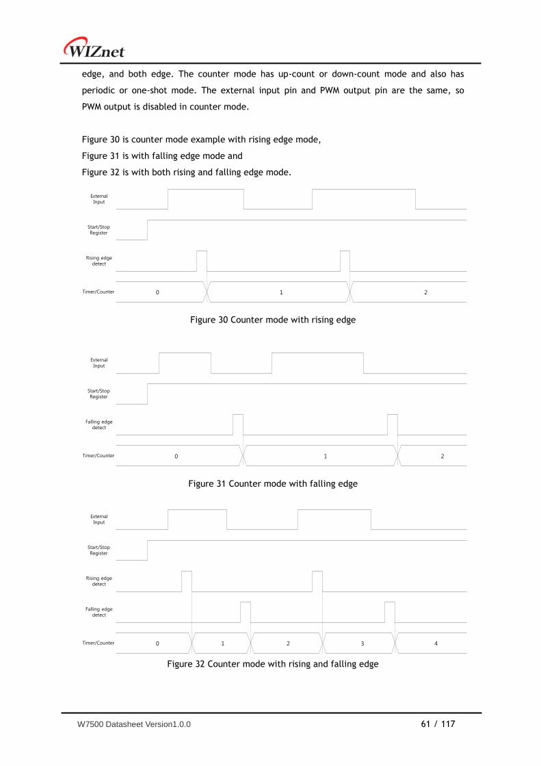
W7500 Datasheet Version1.0.0 61 / 117
edge, and both edge. The counter mode has up-count or down-count mode and also has
periodic or one-shot mode. The external input pin and PWM output pin are the same, so
PWM output is disabled in counter mode.
Figure 30 is counter mode example with rising edge mode,
Figure 31 is with falling edge mode and
Figure 32 is with both rising and falling edge mode.
Figure 30 Counter mode with rising edge
Figure 31 Counter mode with falling edge
Figure 32 Counter mode with rising and falling edge
ExternalInput
Timer/Counter 1 20
Start/StopRegister
Rising edgedetect
ExternalInput
Timer/Counter 1 20
Start/StopRegister
Falling edgedetect
ExternalInput
Timer/Counter 2 40
Start/StopRegister
Rising edgedetect
Falling edgedetect
1 3
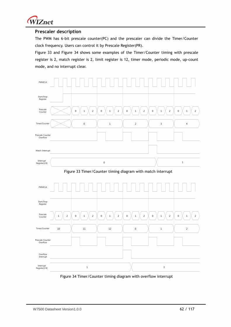
W7500 Datasheet Version1.0.0 62 / 117
Prescaler description
The PWM has 6-bit prescale counter(PC) and the prescaler can divide the Timer/Counter
clock frequency. Users can control it by Prescale Register(PR).
Figure 33 and Figure 34 shows some examples of the Timer/Counter timing with prescale
register is 2, match register is 2, limit register is 12, timer mode, periodic mode, up-count
mode, and no interrupt clear.
Figure 33 Timer/Counter timing diagram with match interrupt
Figure 34 Timer/Counter timing diagram with overflow interrupt
PWMCLK
Start/StopRegister
PrescaleCounter 0 1 2 0 1 2 0 1 2 0 1 2 0 1
Timer/Counter 0 1 2 3 4
Prescale CounterOverflow
2
Match Interrupt
0 1Interrupt
Register[2:0]
PWMCLK
Start/StopRegister
PrescaleCounter 0 1 2 0 1 2 0 1 2 0 1 2 0 1
Timer/Counter 11 12 0 1 2
Prescale CounterOverflow
2
Overflow Interrupt
1 3Interrupt
Register[2:0]
1 2
10
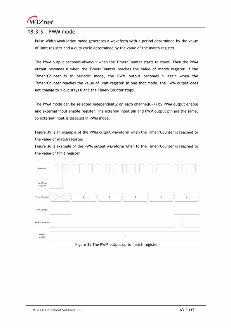
W7500 Datasheet Version1.0.0 63 / 117
PWM mode 18.3.3
Pulse Width Modulation mode generates a waveform with a period determined by the value
of limit register and a duty cycle determined by the value of the match register.
The PWM output becomes always 1 when the Timer/Counter starts to count. Then the PWM
output becomes 0 when the Timer/Counter reaches the value of match register. If the
Timer/Counter is in periodic mode, the PWM output becomes 1 again when the
Timer/Counter reaches the value of limit register. In one-shot mode, the PWM output does
not change to 1 but stays 0 and the Timer/Counter stops.
The PWM mode can be selected independently on each channel(0~7) by PWM output enable
and external input enable register. The external input pin and PWM output pin are the same,
so external input is disabled in PWM mode.
Figure 35 is an example of the PWM output waveform when the Timer/Counter is reached to
the value of match register.
Figure 36 is example of the PWM output waveform when to the Timer/Counter is reached to
the value of limit register.
Figure 35 The PWM output up to match register
PWMCLK
Start/StopRegister
Timer/Counter 0 1 2 3 4
Match Interrupt
Matchregister 3
PWM output
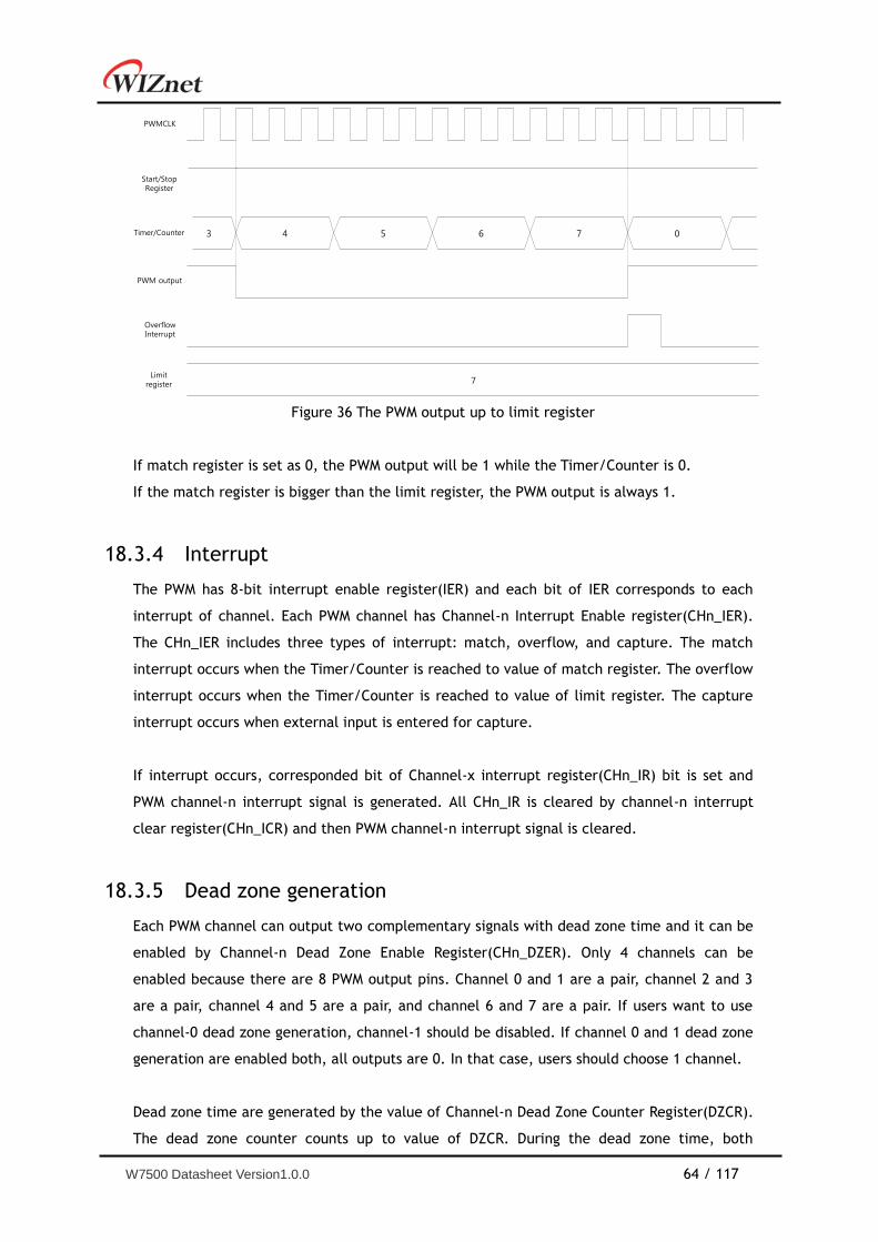
W7500 Datasheet Version1.0.0 64 / 117
Figure 36 The PWM output up to limit register
If match register is set as 0, the PWM output will be 1 while the Timer/Counter is 0.
If the match register is bigger than the limit register, the PWM output is always 1.
Interrupt 18.3.4
The PWM has 8-bit interrupt enable register(IER) and each bit of IER corresponds to each
interrupt of channel. Each PWM channel has Channel-n Interrupt Enable register(CHn_IER).
The CHn_IER includes three types of interrupt: match, overflow, and capture. The match
interrupt occurs when the Timer/Counter is reached to value of match register. The overflow
interrupt occurs when the Timer/Counter is reached to value of limit register. The capture
interrupt occurs when external input is entered for capture.
If interrupt occurs, corresponded bit of Channel-x interrupt register(CHn_IR) bit is set and
PWM channel-n interrupt signal is generated. All CHn_IR is cleared by channel-n interrupt
clear register(CHn_ICR) and then PWM channel-n interrupt signal is cleared.
Dead zone generation 18.3.5
Each PWM channel can output two complementary signals with dead zone time and it can be
enabled by Channel-n Dead Zone Enable Register(CHn_DZER). Only 4 channels can be
enabled because there are 8 PWM output pins. Channel 0 and 1 are a pair, channel 2 and 3
are a pair, channel 4 and 5 are a pair, and channel 6 and 7 are a pair. If users want to use
channel-0 dead zone generation, channel-1 should be disabled. If channel 0 and 1 dead zone
generation are enabled both, all outputs are 0. In that case, users should choose 1 channel.
Dead zone time are generated by the value of Channel-n Dead Zone Counter Register(DZCR).
The dead zone counter counts up to value of DZCR. During the dead zone time, both
PWMCLK
Start/StopRegister
Timer/Counter 4 5 6 7 0
Overflow Interrupt
Limitregister 7
PWM output
3
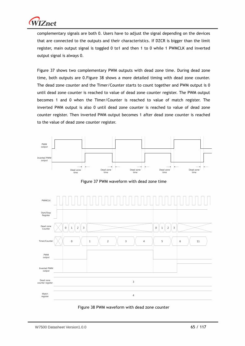
W7500 Datasheet Version1.0.0 65 / 117
complementary signals are both 0. Users have to adjust the signal depending on the devices
that are connected to the outputs and their characteristics. If DZCR is bigger than the limit
register, main output signal is toggled 0 to1 and then 1 to 0 while 1 PWMCLK and inverted
output signal is always 0.
Figure 37 shows two complementary PWM outputs with dead zone time. During dead zone
time, both outputs are 0.Figure 38 shows a more detailed timing with dead zone counter.
The dead zone counter and the Timer/Counter starts to count together and PWM output is 0
until dead zone counter is reached to value of dead zone counter register. The PWM output
becomes 1 and 0 when the Timer/Counter is reached to value of match register. The
inverted PWM output is also 0 until dead zone counter is reached to value of dead zone
counter register. Then inverted PWM output becomes 1 after dead zone counter is reached
to the value of dead zone counter register.
Figure 37 PWM waveform with dead zone time
Figure 38 PWM waveform with dead zone counter
PWMoutput
Inverted PWMoutput
Dead zonetime
Dead zonetime
Dead zonetime
Dead zonetime
Dead zonetime
PWMCLK
Start/StopRegister
Dead zoneCounter
Timer/Counter 0
PWMoutput
3Dead zone
counter register
0 1 2 3
1 2 3 4 5 6 11
0 1 2 3
Inverted PWMoutput
4Matchregister
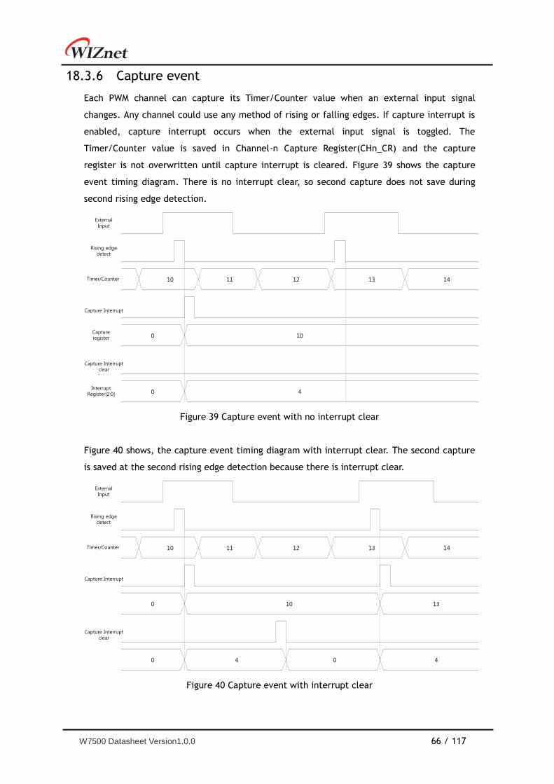
W7500 Datasheet Version1.0.0 66 / 117
Capture event 18.3.6
Each PWM channel can capture its Timer/Counter value when an external input signal
changes. Any channel could use any method of rising or falling edges. If capture interrupt is
enabled, capture interrupt occurs when the external input signal is toggled. The
Timer/Counter value is saved in Channel-n Capture Register(CHn_CR) and the capture
register is not overwritten until capture interrupt is cleared. Figure 39 shows the capture
event timing diagram. There is no interrupt clear, so second capture does not save during
second rising edge detection.
Figure 39 Capture event with no interrupt clear
Figure 40 shows, the capture event timing diagram with interrupt clear. The second capture
is saved at the second rising edge detection because there is interrupt clear.
Figure 40 Capture event with interrupt clear
ExternalInput
Timer/Counter 12 14
Rising edgedetect
11 1310
Capture Interrupt
10Captureregister 0
4Interrupt
Register[2:0] 0
Capture Interruptclear
ExternalInput
Timer/Counter 12 14
Rising edgedetect
11 1310
Capture Interrupt
100
00
Capture Interruptclear
4 4
13
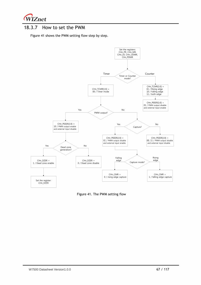
W7500 Datasheet Version1.0.0 67 / 117
How to set the PWM 18.3.7
Figure 41 shows the PWM setting flow step by step.
Figure 41. The PWM setting flow
Set the registers:CHn_PR, CHn_MR,
CHn_LR, CHn_UDMR, CHn_PDMR
Timer or Countermode?
CHn_TCMR[1:0] = 00 / Timer mode
CHn_TCMR[1:0] = 01 / Rising edge 10 / Falling edge 11 / both edge
Timer Counter
PWM output?
Yes No
CHn_PEEER[1:0] = 10 / PWM output enable
and external input disableCapture?
Yes No
CHn_PEEER[1:0] = 01 / PWM output disable
and external input enable
CHn_PEEER[1:0] = 00, 11 / PWM output disable
and external input disable
Capture mode?
Falling edge
Rising edge
CHn_CMR = 0 / rising edge capture
CHn_CMR = 1 / falling edge capture
Dead zonegeneration?
Yes No
CHn_DZER =1 / Dead zone enable
CHn_DZER =0 / Dead zone disable
Set the register:CHn_DZER
CHn_PEEER[1:0] = 01 / PWM output disable
and external input enable
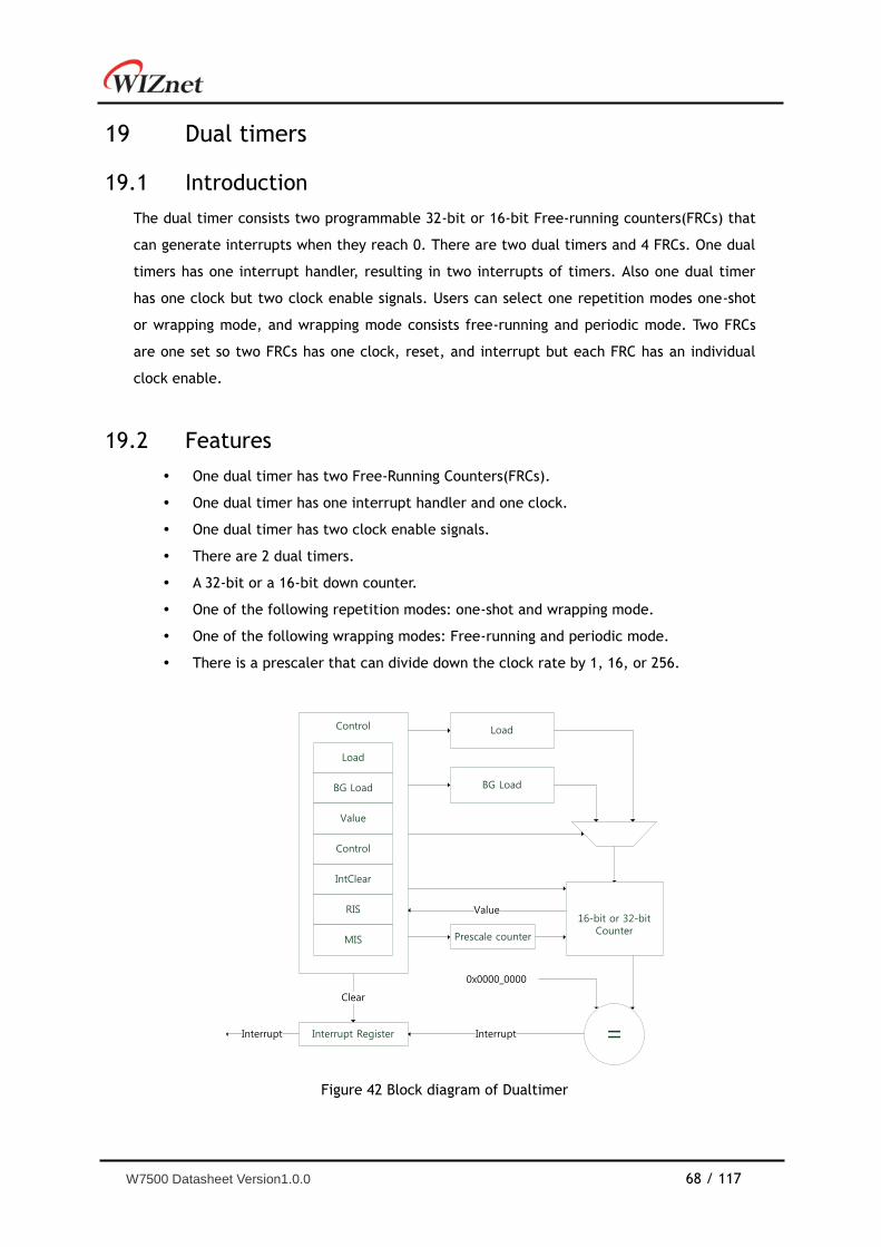
W7500 Datasheet Version1.0.0 68 / 117
19 Dual timers
Introduction 19.1
The dual timer consists two programmable 32-bit or 16-bit Free-running counters(FRCs) that
can generate interrupts when they reach 0. There are two dual timers and 4 FRCs. One dual
timers has one interrupt handler, resulting in two interrupts of timers. Also one dual timer
has one clock but two clock enable signals. Users can select one repetition modes one-shot
or wrapping mode, and wrapping mode consists free-running and periodic mode. Two FRCs
are one set so two FRCs has one clock, reset, and interrupt but each FRC has an individual
clock enable.
Features 19.2
One dual timer has two Free-Running Counters(FRCs).
One dual timer has one interrupt handler and one clock.
One dual timer has two clock enable signals.
There are 2 dual timers.
A 32-bit or a 16-bit down counter.
One of the following repetition modes: one-shot and wrapping mode.
One of the following wrapping modes: Free-running and periodic mode.
There is a prescaler that can divide down the clock rate by 1, 16, or 256.
Figure 42 Block diagram of Dualtimer
Load
BG Load
16-bit or 32-bitCounter
=
0x0000_0000
Prescale counter
Interrupt Register InterruptInterrupt
Control
BG Load
Value
Control
IntClear
RIS
MIS
Load
Clear
Value
W7500 Datasheet Version1.0.0 69 / 117
Functional description 19.3
Clock and clock enable 19.3.1
The dual timers contain PCLK and TIMERCLK clock inputs. PCLK is the main APB system clock
and is used by the register interface. TIMERCLK is the input to the prescale units and the
decrementing counters. PCLK and TIMERCLK are synchronous.
The dual timers consist two programmable 32-bit Free-Running Counters(FRC) which operate
independently. The two timers operate from one TIMERCLK but Each FRC is controlled
independently by individual clock enable.
Timer size 19.3.2
Users can select FRC as 16-bit or 32-bit using the control register.
Prescaler 19.3.3
The timer has a prescaler that can divide down the enabled clock rate by 1, 16 or 256.
Repetition mode 19.3.4
There are two repetition mode: one-shot and wrapping mode. Wrapping mode has two
modes: free-running and periodic mode.
One-shot mode
The counter generates an interrupt once. When the counter reaches 0, it halts until
users reprogram it. Users can do this as below:
Clear the one-shot count bit in the control register, in which case the count
proceeds according to the selection of wrapping mode(free-running or
periodic mode).
Write a new value to the Load Value register.
Wrapping mode
Free-running mode
The counter wraps after reaching its zero value, and continues to count down from
the maximum value. This is the default mode.
Periodic mode
The counter generates an interrupt at a constant interval, reloading the original
value after wrapping past zero.
W7500 Datasheet Version1.0.0 70 / 117
Interrupt 19.3.5
An interrupt is generated when the counter reaches 0 and is only cleared when the interrupt
clear register is accessed.
The register holds the value until the interrupt is cleared.
Users can mask interrupts by writing 0 to the Interrupt Enable bit in the control register.
Users can read the following from status registers:
Raw interrupt status before masking.
Final interrupt status after masking.
The interrupts from the individual timers after masking are logically ORed into a combined
interrupt.
Operation 19.3.6
The operation of each timer is identical. The timer is loaded by writing to the load register
and counts down to 0 if enabled. When a counter is already running, writing to the load
register causes the counter to immediately restart at the new value. Writing to the
background load value has no effect on the current count. In periodic mode, the counter
continues to decrease to 0 and restart from the new load value.
An interrupt is generated when 0 is reached. Users can clear the interrupt by writing to the
clear register. If users select one-shot mode, the counter halts when it reaches 0 until users
deselect one-shot mode or write a new load value.
Otherwise, after reaching a zero count, if the timer is operating in free-running mode, it
continues to decrease from its maximum value. If users select periodic mode, the timer
reloads the count value from the load register and continues to decrease. In this mode, the
counter effectively generates a periodic interrupt.
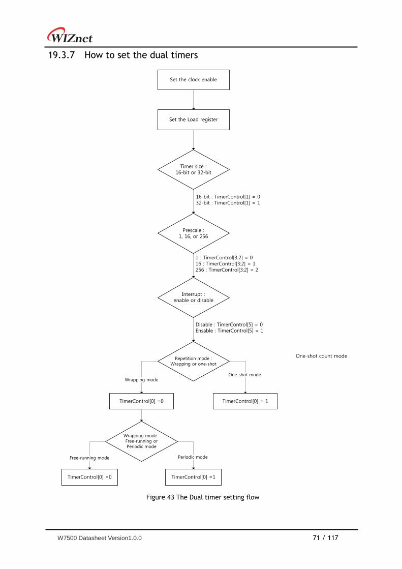
W7500 Datasheet Version1.0.0 71 / 117
How to set the dual timers 19.3.7
Figure 43 The Dual timer setting flow
Set the clock enable
Set the Load register
Timer size : 16-bit or 32-bit
16-bit : TimerControl[1] = 032-bit : TimerControl[1] = 1
Prescale :1, 16, or 256
1 : TimerControl[3:2] = 016 : TimerControl[3:2] = 1256 : TimerControl[3:2] = 2
Interrupt : enable or disable
Disable : TimerControl[5] = 0Ensable : TimerControl[5] = 1
Repetition mode :Wrapping or one-shot
One-shot mode
TimerControl[0] = 1
One-shot count mode
Wrapping mode :Free-running orPeriodic mode
Wrapping mode
TimerControl[0] =0
TimerControl[0] =1
Periodic modeFree-running mode
TimerControl[0] =0
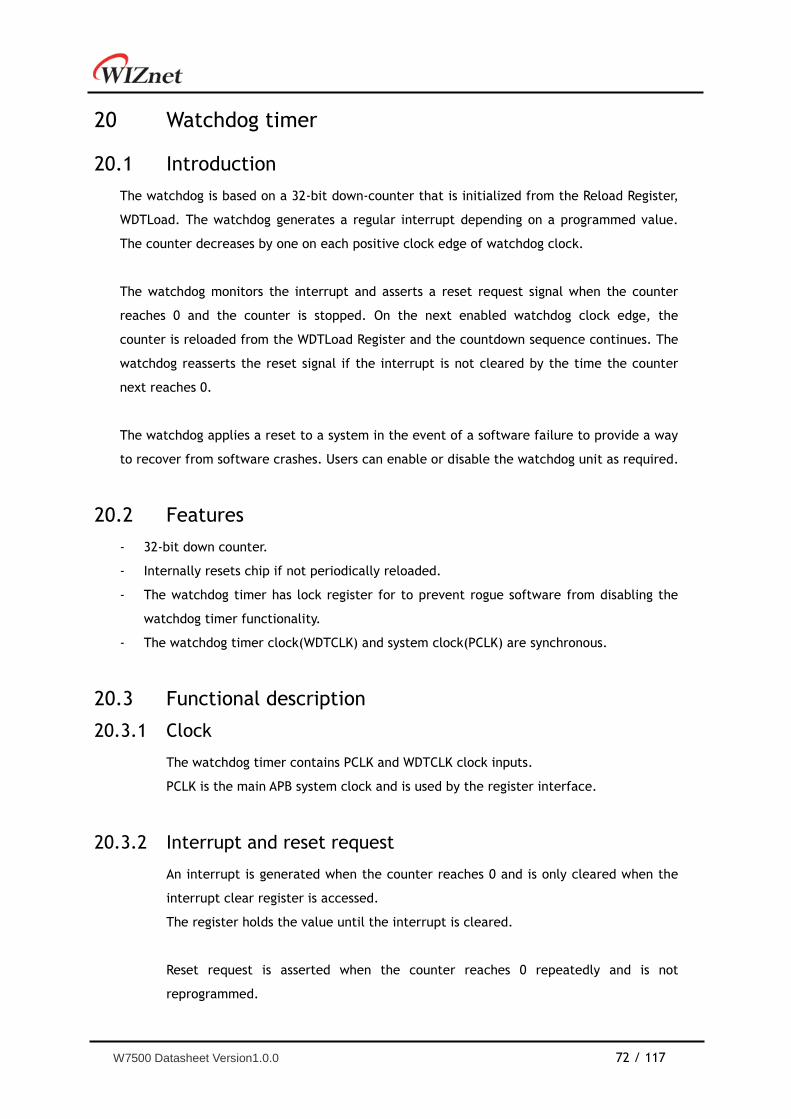
W7500 Datasheet Version1.0.0 72 / 117
20 Watchdog timer
20.1 Introduction
The watchdog is based on a 32-bit down-counter that is initialized from the Reload Register,
WDTLoad. The watchdog generates a regular interrupt depending on a programmed value.
The counter decreases by one on each positive clock edge of watchdog clock.
The watchdog monitors the interrupt and asserts a reset request signal when the counter
reaches 0 and the counter is stopped. On the next enabled watchdog clock edge, the
counter is reloaded from the WDTLoad Register and the countdown sequence continues. The
watchdog reasserts the reset signal if the interrupt is not cleared by the time the counter
next reaches 0.
The watchdog applies a reset to a system in the event of a software failure to provide a way
to recover from software crashes. Users can enable or disable the watchdog unit as required.
20.2 Features
- 32-bit down counter.
- Internally resets chip if not periodically reloaded.
- The watchdog timer has lock register for to prevent rogue software from disabling the
watchdog timer functionality.
- The watchdog timer clock(WDTCLK) and system clock(PCLK) are synchronous.
20.3 Functional description
Clock 20.3.1
The watchdog timer contains PCLK and WDTCLK clock inputs.
PCLK is the main APB system clock and is used by the register interface.
Interrupt and reset request 20.3.2
An interrupt is generated when the counter reaches 0 and is only cleared when the
interrupt clear register is accessed.
The register holds the value until the interrupt is cleared.
Reset request is asserted when the counter reaches 0 repeatedly and is not
reprogrammed.
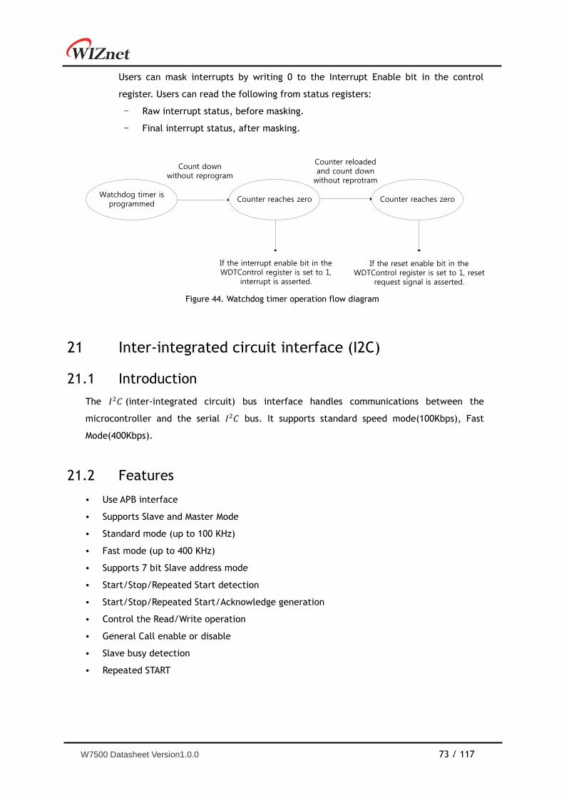
W7500 Datasheet Version1.0.0 73 / 117
Users can mask interrupts by writing 0 to the Interrupt Enable bit in the control
register. Users can read the following from status registers:
- Raw interrupt status, before masking.
- Final interrupt status, after masking.
Figure 44. Watchdog timer operation flow diagram
21 Inter-integrated circuit interface (I2C)
Introduction 21.1
The 𝐼2𝐶 (inter-integrated circuit) bus interface handles communications between the
microcontroller and the serial 𝐼2𝐶 bus. It supports standard speed mode(100Kbps), Fast
Mode(400Kbps).
Features 21.2
• Use APB interface
• Supports Slave and Master Mode
• Standard mode (up to 100 KHz)
• Fast mode (up to 400 KHz)
• Supports 7 bit Slave address mode
• Start/Stop/Repeated Start detection
• Start/Stop/Repeated Start/Acknowledge generation
• Control the Read/Write operation
• General Call enable or disable
• Slave busy detection
• Repeated START
Watchdog timer is programmed
Counter reaches zero Counter reaches zero
Count down without reprogram
Counter reloaded and count down
without reprotram
If the interrupt enable bit in the WDTControl register is set to 1,
interrupt is asserted.
If the reset enable bit in the WDTControl register is set to 1, reset
request signal is asserted.
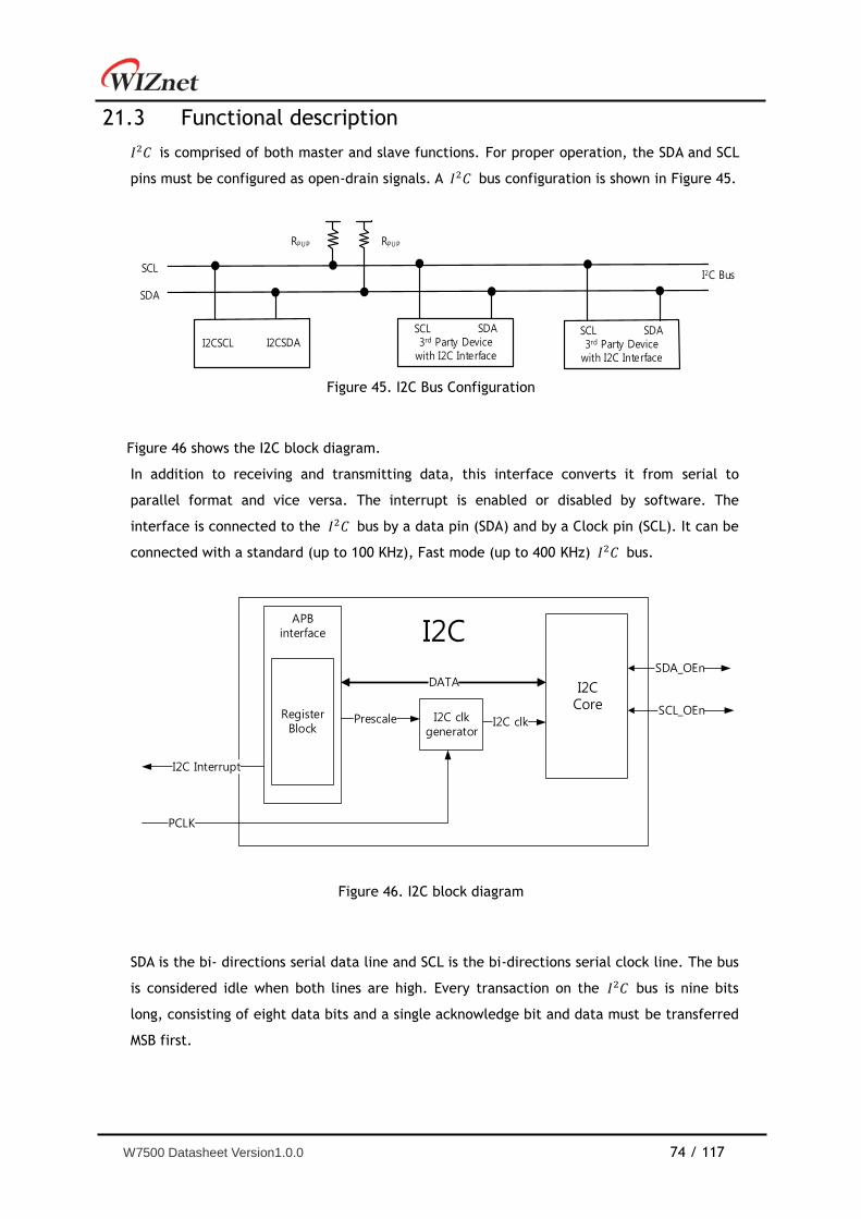
W7500 Datasheet Version1.0.0 74 / 117
Functional description 21.3
𝐼2𝐶 is comprised of both master and slave functions. For proper operation, the SDA and SCL
pins must be configured as open-drain signals. A 𝐼2𝐶 bus configuration is shown in Figure 45.
Figure 45. I2C Bus Configuration
Figure 46 shows the I2C block diagram.
In addition to receiving and transmitting data, this interface converts it from serial to
parallel format and vice versa. The interrupt is enabled or disabled by software. The
interface is connected to the 𝐼2𝐶 bus by a data pin (SDA) and by a Clock pin (SCL). It can be
connected with a standard (up to 100 KHz), Fast mode (up to 400 KHz) 𝐼2𝐶 bus.
I2C
I2C Interrupt
APB interface
RegisterBlock
I2CCore
SDA_OEn
I2C clkgenerator
Prescale
PCLK
SCL_OEnI2C clk
DATA
Figure 46. I2C block diagram
SDA is the bi- directions serial data line and SCL is the bi-directions serial clock line. The bus
is considered idle when both lines are high. Every transaction on the 𝐼2𝐶 bus is nine bits
long, consisting of eight data bits and a single acknowledge bit and data must be transferred
MSB first.
RPUP
SDA
RPUP
SCLI2C Bus
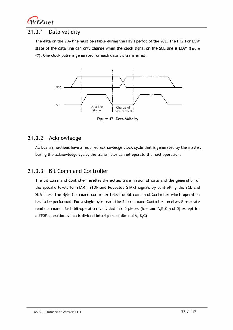
W7500 Datasheet Version1.0.0 75 / 117
Data validity 21.3.1
The data on the SDA line must be stable during the HIGH period of the SCL. The HIGH or LOW
state of the data line can only change when the clock signal on the SCL line is LOW (Figure
47). One clock pulse is generated for each data bit transferred.
SDA
SCLData lineStable
Change of data allowed
Figure 47. Data Validity
Acknowledge 21.3.2
All bus transactions have a required acknowledge clock cycle that is generated by the master.
During the acknowledge cycle, the transmitter cannot operate the next operation.
Bit Command Controller 21.3.3
The Bit command Controller handles the actual transmission of data and the generation of
the specific levels for START, STOP and Repeated START signals by controlling the SCL and
SDA lines. The Byte Command controller tells the Bit command Controller which operation
has to be performed. For a single byte read, the Bit command Controller receives 8 separate
read command. Each bit-operation is divided into 5 pieces (idle and A,B,C,and D) except for
a STOP operation which is divided into 4 pieces(idle and A, B,C)
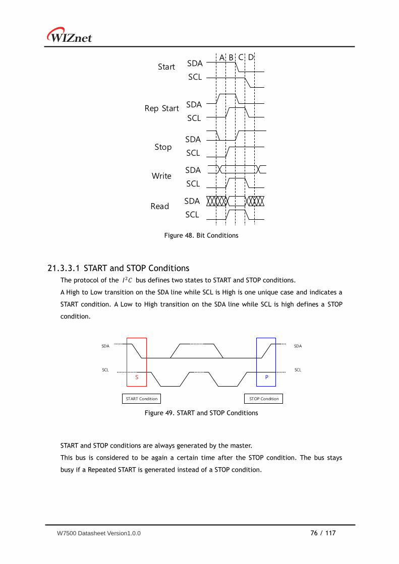
W7500 Datasheet Version1.0.0 76 / 117
A B C D
SCL
SDAStart
Rep Start
Stop
Write
Read
SCL
SDA
SCL
SDA
SCL
SDA
SCL
SDA
Figure 48. Bit Conditions
21.3.3.1 START and STOP Conditions
The protocol of the 𝐼2𝐶 bus defines two states to START and STOP conditions.
A High to Low transition on the SDA line while SCL is High is one unique case and indicates a
START condition. A Low to High transition on the SDA line while SCL is high defines a STOP
condition.
S P
SDA
SCL
SDA
SCL
START Condition STOP Condition
Figure 49. START and STOP Conditions
START and STOP conditions are always generated by the master.
This bus is considered to be again a certain time after the STOP condition. The bus stays
busy if a Repeated START is generated instead of a STOP condition.
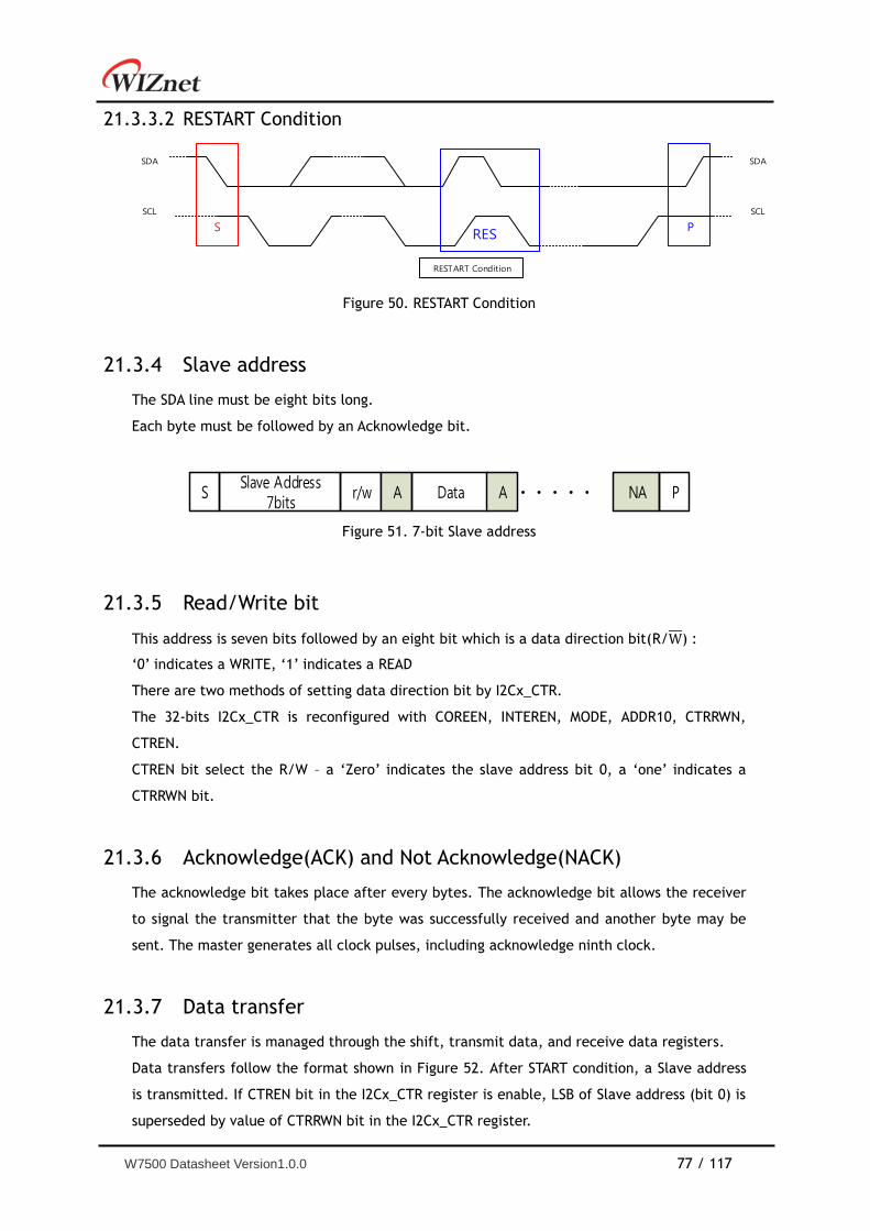
W7500 Datasheet Version1.0.0 77 / 117
21.3.3.2 RESTART Condition
S P
SDA
SCL
SDA
SCL
RES
RESTART Condition
Figure 50. RESTART Condition
Slave address 21.3.4
The SDA line must be eight bits long.
Each byte must be followed by an Acknowledge bit.
SSlave Address
7bitsr/w A Data A NA P
Figure 51. 7-bit Slave address
Read/Write bit 21.3.5
This address is seven bits followed by an eight bit which is a data direction bit(R/W) :
„0‟ indicates a WRITE, „1‟ indicates a READ
There are two methods of setting data direction bit by I2Cx_CTR.
The 32-bits I2Cx_CTR is reconfigured with COREEN, INTEREN, MODE, ADDR10, CTRRWN,
CTREN.
CTREN bit select the R/W – a „Zero‟ indicates the slave address bit 0, a „one‟ indicates a
CTRRWN bit.
Acknowledge(ACK) and Not Acknowledge(NACK) 21.3.6
The acknowledge bit takes place after every bytes. The acknowledge bit allows the receiver
to signal the transmitter that the byte was successfully received and another byte may be
sent. The master generates all clock pulses, including acknowledge ninth clock.
Data transfer 21.3.7
The data transfer is managed through the shift, transmit data, and receive data registers.
Data transfers follow the format shown in Figure 52. After START condition, a Slave address
is transmitted. If CTREN bit in the I2Cx_CTR register is enable, LSB of Slave address (bit 0) is
superseded by value of CTRRWN bit in the I2Cx_CTR register.
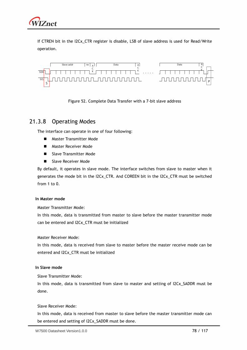
W7500 Datasheet Version1.0.0 78 / 117
If CTREN bit in the I2Cx_CTR register is disable, LSB of slave address is used for Read/Write
operation.
S
SDA
SCL
Slave addr rw Data Data
P
ACK
ACK
ACK
Figure 52. Complete Data Transfer with a 7-bit slave address
Operating Modes 21.3.8
The interface can operate in one of four following:
Master Transmitter Mode
Master Receiver Mode
Slave Transmitter Mode
Slave Receiver Mode
By default, it operates in slave mode. The interface switches from slave to master when it
generates the mode bit in the I2Cx_CTR. And COREEN bit in the I2Cx_CTR must be switched
from 1 to 0.
In Master mode
Master Transmitter Mode:
In this mode, data is transmitted from master to slave before the master transmitter mode
can be entered and I2Cx_CTR must be initialized
Master Receiver Mode:
In this mode, data is received from slave to master before the master receive mode can be
entered and I2Cx_CTR must be initialized
In Slave mode
Slave Transmitter Mode:
In this mode, data is transmitted from slave to master and setting of I2Cx_SADDR must be
done.
Slave Receiver Mode:
In this mode, data is received from master to slave before the master transmitter mode can
be entered and setting of I2Cx_SADDR must be done.
W7500 Datasheet Version1.0.0 79 / 117
Interrupts 21.3.9
The 𝐼2𝐶 can generate interrupt when the following conditions are observed:
Start conditions on bus detected
Stop conditions on bus detected
Timeout error
Master transaction completed
Slave transaction received
𝐼2𝐶 bus have separate interrupt signals.
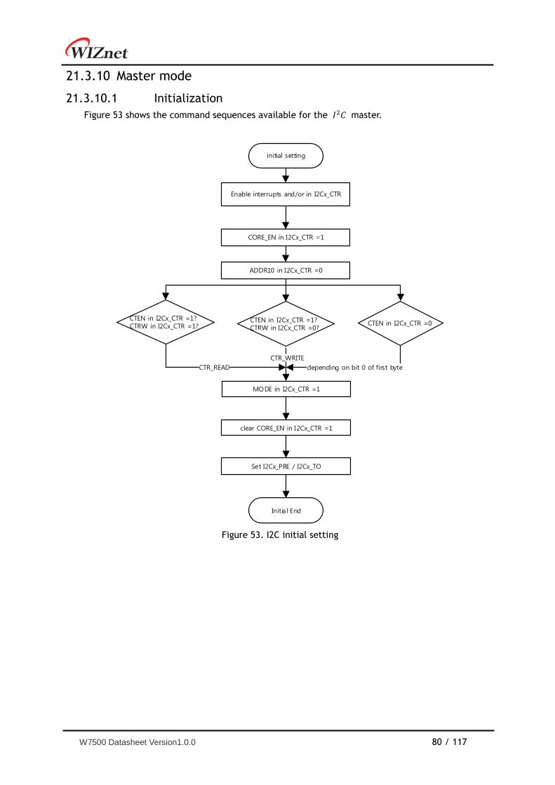
W7500 Datasheet Version1.0.0 80 / 117
Master mode 21.3.10
21.3.10.1 Initialization
Figure 53 shows the command sequences available for the 𝐼2𝐶 master.
initial setting
Enable interrupts and/or in I2Cx_CTR
MODE in I2Cx_CTR =1
clear CORE_EN in I2Cx_CTR =1
Set I2Cx_PRE / I2Cx_TO
Initia l End
CORE_EN in I2Cx_CTR =1
CTEN in I2Cx_CTR =1? CTRW in I2Cx_CTR =1?
ADDR10 in I2Cx_CTR =0
CTEN in I2Cx_CTR =1? CTRW in I2Cx_CTR =0?
CTEN in I2Cx_CTR =0
CTR_READ depending on bit 0 of first byte
CTR_WRITE
Figure 53. I2C initial setting
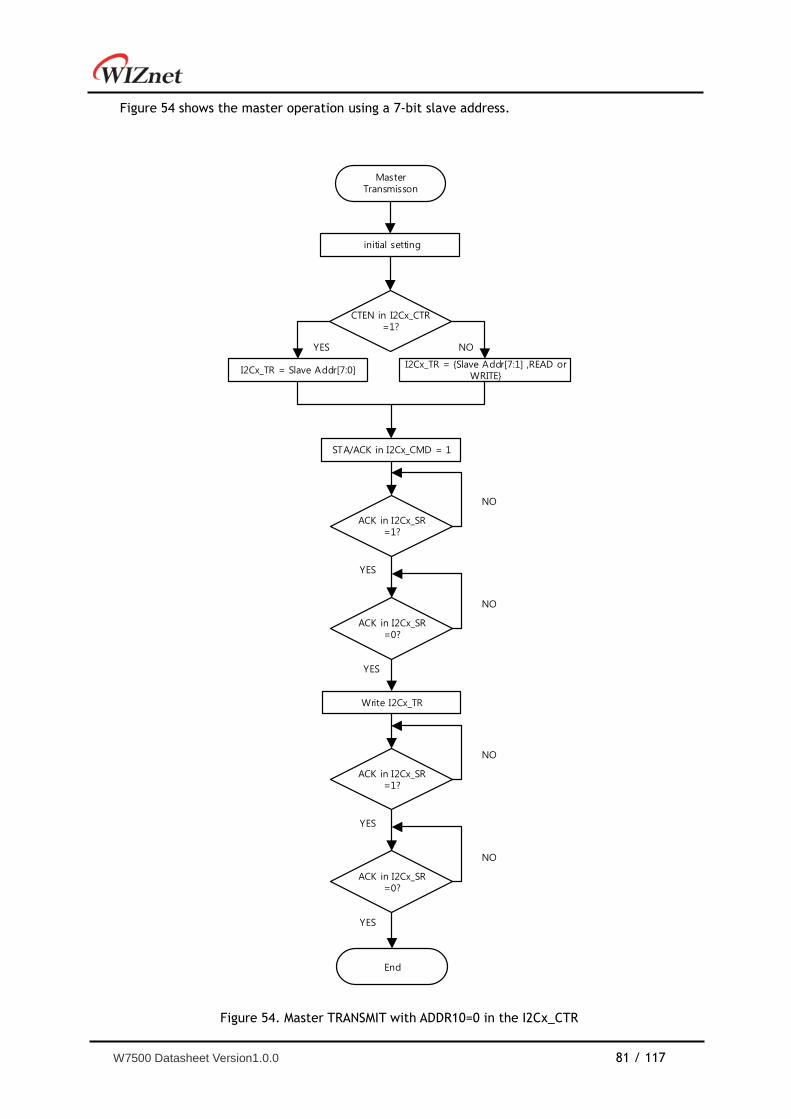
W7500 Datasheet Version1.0.0 81 / 117
Figure 54 shows the master operation using a 7-bit slave address.
MasterTransmisson
initial setting
CTEN in I2Cx_CTR=1?
YES
I2Cx_TR = Slave Addr[7:0]I2Cx_TR = {Slave Addr[7:1] ,READ or
WRITE}
NO
STA/ACK in I2Cx_CMD = 1
ACK in I2Cx_SR=1?
YES
ACK in I2Cx_SR=0?
NO
NO
Write I2Cx_TR
YES
ACK in I2Cx_SR=1?
YES
ACK in I2Cx_SR=0?
NO
NO
YES
End
Figure 54. Master TRANSMIT with ADDR10=0 in the I2Cx_CTR
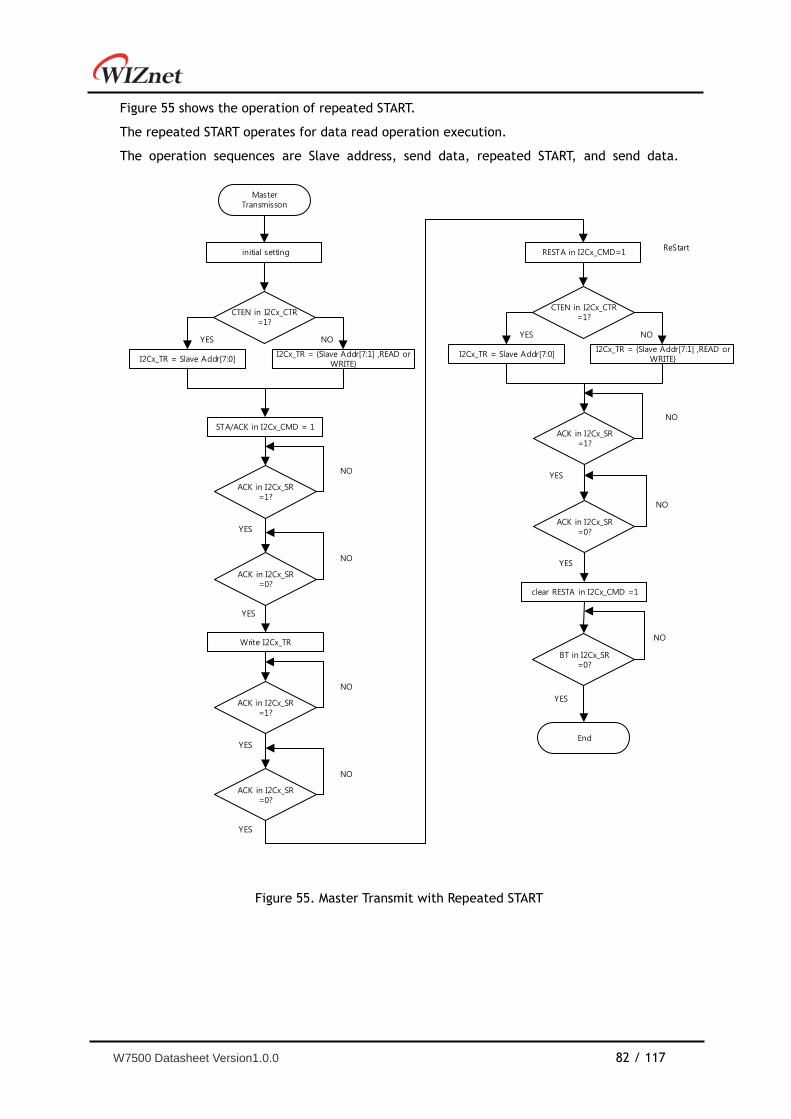
W7500 Datasheet Version1.0.0 82 / 117
Figure 55 shows the operation of repeated START.
The repeated START operates for data read operation execution.
The operation sequences are Slave address, send data, repeated START, and send data.
MasterTransmisson
initial setting
CTEN in I2Cx_CTR=1?
YES
I2Cx_TR = Slave Addr[7:0]I2Cx_TR = {Slave Addr[7:1] ,READ or
WRITE}
NO
STA/ACK in I2Cx_CMD = 1
ACK in I2Cx_SR=1?
YES
ACK in I2Cx_SR=0?
NO
NO
Write I2Cx_TR
YES
ACK in I2Cx_SR=1?
YES
ACK in I2Cx_SR=0?
NO
NO
YES
End
RESTA in I2Cx_CMD=1ReStart
CTEN in I2Cx_CTR=1?
YES
I2Cx_TR = Slave Addr[7:0]I2Cx_TR = {Slave Addr[7:1] ,READ or
WRITE}
NO
ACK in I2Cx_SR=1?
ACK in I2Cx_SR=0?
NO
YES
NO
YES
clear RESTA in I2Cx_CMD =1
BT in I2Cx_SR=0?
YES
NO
Figure 55. Master Transmit with Repeated START
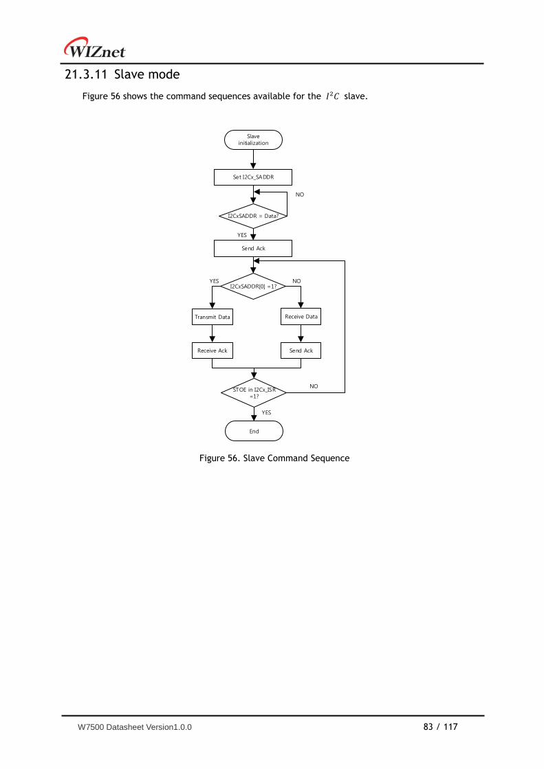
W7500 Datasheet Version1.0.0 83 / 117
Slave mode 21.3.11
Figure 56 shows the command sequences available for the 𝐼2𝐶 slave.
Slaveinitialization
Set I2Cx_SADDR
I2CxSADDR = Data?
Send Ack
NO
YES
I2CxSADDR[0] =1?
Transmit Data Receive Data
Send AckReceive Ack
End
STOE in I2Cx_ISR =1?
NOYES
YES
NO
Figure 56. Slave Command Sequence
W7500 Datasheet Version1.0.0 84 / 117
22 UART(Universal Asynchronous Receive Transmit)
Introduction 22.1
The UART supports synchronous one-way communication, half-duplex single wire
communication, and multiprocessor communications(CTS/RTS).
Features 22.2
- Serial-to-parallel conversion on data received from a peripheral device
- Parallel-to-serial conversion on data transmitted to the peripheral device
- Data size of 5,6,7 and 8 its
- One or two stop bits
- Even, odd, stick, or no-parity bit generation and detection
- Support of hardware flow control
- Programmable FIFO disabling for 1-byte depth.
- Programmable use of UART or IrDA SIR input/output
- False start bit detection
Functional description 22.3
UART bidirectional communication requires a minimum of two pins: RX, TX
The frame are comprised of:
An Idle Line prior to transmission or reception
A start bit
A data word (8 or 9 bits) least significant bit first
1, 1.5, 2 Stop bits indicating that the frame is complete
The USART interface uses a baud rate generator
A status register (UART1_RISR)
data registers (UART1DR) A baud rate register (UART1_IBRD,UART1_FBRD)
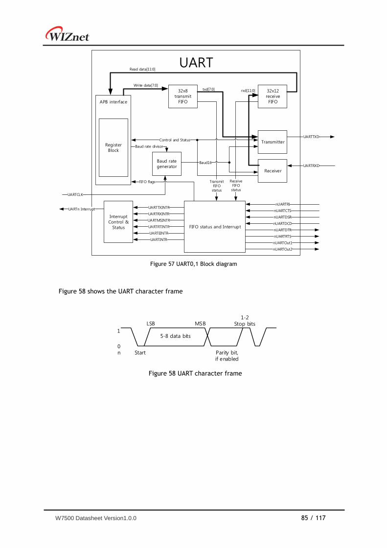
W7500 Datasheet Version1.0.0 85 / 117
Figure 57 UART0,1 Block diagram
Figure 58 shows the UART character frame
Figure 58 UART character frame
UART
FIFO status and Interrupt
UARTn Interrupt
Interrupt Control &
Status
UARTTXINTR
APB interface
RegisterBlock
32x8transmit
FIFO
32x12receiveFIFO
Transmitter
Receiver
UARTRXINTR
UARTMSINTR
UARTRTINTR
UARTEINTR
UARTINTR
nUARTRI
nUARTCTS
nUARTDSR
nUARTDCD
nUARTDTR
nUARTRTS
nUARTOut1
nUARTOut2
UARTRXD
UARTTXD
Baud rategenerator
Read data[11:0]
Write data[7:0]txd[7:0] rxd[11:0]
Control and Status
Baud rate divisor
Baud16
TransmitFIFOstatus
ReceiveFIFOstatus
FIFO flags
UARTCLK
1
0n Start
5-8 data bits
LSB MSB
Parity bit,if enabled
1-2Stop bits
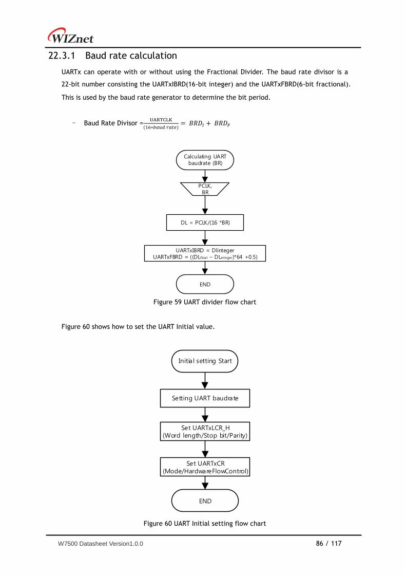
W7500 Datasheet Version1.0.0 86 / 117
Baud rate calculation 22.3.1
UARTx can operate with or without using the Fractional Divider. The baud rate divisor is a
22-bit number consisting the UARTxIBRD(16-bit integer) and the UARTxFBRD(6-bit fractional).
This is used by the baud rate generator to determine the bit period.
- Baud Rate Divisor =UARTCLK
(16∗𝑏𝑎𝑢𝑑 𝑟𝑎𝑡𝑒)= 𝐵𝑅𝐷𝐼 + 𝐵𝑅𝐷𝐹
Figure 59 UART divider flow chart
Figure 60 shows how to set the UART Initial value.
Figure 60 UART Initial setting flow chart
DL = PCLK/(16 *BR)
UARTxIBRD = DlintegerUARTxFBRD = ((DLfloat – DLinteger)*64 +0.5)
END
Calculating UART baudrate (BR)
PCLK,BR
Initia l setting Start
Set UARTxLCR_H(Word length/Stop bit/Parity)
Set UARTxCR(Mode/HardwareFlowControl)
END
Setting UART baudrate
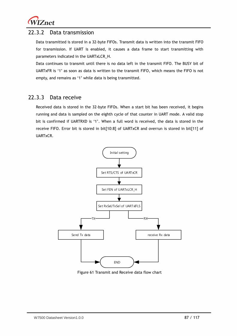
W7500 Datasheet Version1.0.0 87 / 117
Data transmission 22.3.2
Data transmitted is stored in a 32-byte FIFOs. Transmit data is written into the transmit FIFO
for transmission. If UART is enabled, it causes a data frame to start transmitting with
parameters indicated in the UARTxLCR_H.
Data continues to transmit until there is no data left in the transmit FIFO. The BUSY bit of
UARTxFR is „1‟ as soon as data is written to the transmit FIFO, which means the FIFO is not
empty, and remains as „1‟ while data is being transmitted.
Data receive 22.3.3
Received data is stored in the 32-byte FIFOs. When a start bit has been received, it begins
running and data is sampled on the eighth cycle of that counter in UART mode. A valid stop
bit is confirmed if UARTRXD is „1‟. When a full word is received, the data is stored in the
receive FIFO. Error bit is stored in bit[10:8] of UARTxCR and overrun is stored in bit[11] of
UARTxCR.
Figure 61 Transmit and Receive data flow chart
Initia l setting
Set RTS/CTS of UARTxCR
Set FEN of UARTxLCR_H
Set RxSel/TxSel of UARTxIFLS
TX RX
END
Send Tx data receive Rx data
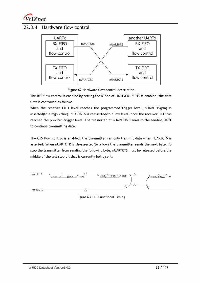
W7500 Datasheet Version1.0.0 88 / 117
Hardware flow control 22.3.4
Figure 62 Hardware flow control description
The RTS flow control is enabled by setting the RTSen of UARTxCR. If RTS is enabled, the data
flow is controlled as follows.
When the receiver FIFO level reaches the programmed trigger level, nUARTRTS(pin) is
asserted(to a high value). nUARTRTS is reasserted(to a low level) once the receiver FIFO has
reached the previous trigger level. The reasserted of nUARTRTS signals to the sending UART
to continue transmitting data.
The CTS flow control is enabled, the transmitter can only transmit data when nUARTCTS is
asserted. When nUARTCTR is de-asserted(to a low) the transmitter sends the next byte. To
stop the transmitter from sending the following byte, nUARTCTS must be released before the
middle of the last stop bit that is currently being sent.
Figure 63 CTS Functional Timing
UARTx
RX FIFOand
flow control
TX FIFOand
flow control
another UARTx
RX FIFOand
flow control
TX FIFOand
flow control
nUARTRTS nUARTRTS
nUARTCTS nUARTCTS
UARTx_TXstart bit0..7 stop start bits0..7 stop start bits0..7 stop
nUARTCTS
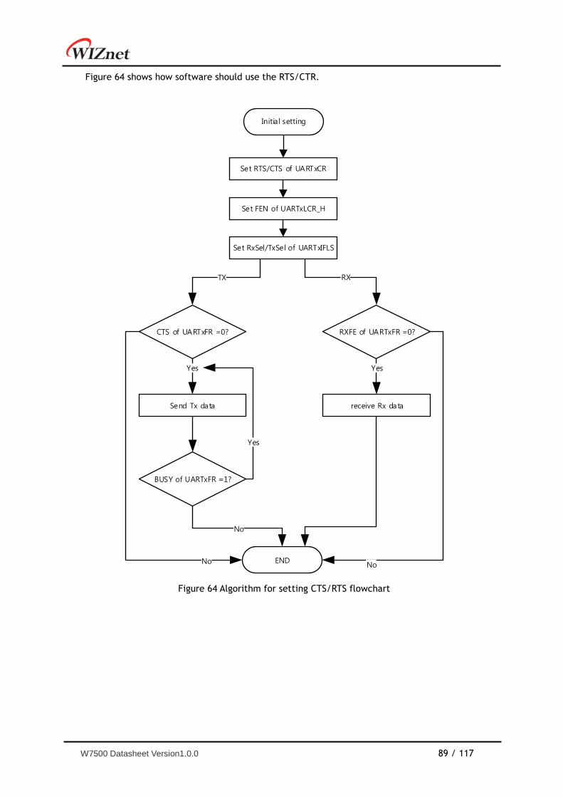
W7500 Datasheet Version1.0.0 89 / 117
Figure 64 shows how software should use the RTS/CTR.
Figure 64 Algorithm for setting CTS/RTS flowchart
Initia l setting
Set RTS/CTS of UARTxCR
Set FEN of UARTxLCR_H
Set RxSel/TxSel of UARTxIFLS
RXFE of UARTxFR =0?CTS of UARTxFR =0?
BUSY of UARTxFR =1?
TX RX
Yes
Yes
No
No END
Send Tx data
Yes
receive Rx data
No
W7500 Datasheet Version1.0.0 90 / 117
23 Synchronous Serial Port (SSP)
Introduction 23.1
The SSP block is an IP provided by ARM (PL022 “PrimeCell® Synchronous Serial Port”).
Additional details about its functional blocks may be found in “ARM PrimeCell® Synchronous
Serial Port (PL022) Technical Reference Manual”.
Features 23.2
• The SSP is a master or slave interface that enables synchronous serial communication
with slave or master peripherals having one of the following:
A MOTOROLA SPI-compatible interface
A TEXAS INSTRUMENTS synchronous serial interface
A National Semiconductor MICROWIRE® interface.
• The SPI interface operates as a master or slave interface. It supports bit rates up to 2
MHz and higher in both master and slave configurations. The SPI has the following
features:
Parallel-to-serial conversion on data written to an internal 16-bit wide, 8-
location deep transmit FIFO
Serial-to-parallel conversion on received data, buffering it in a 16-bit wide, 8-
location deep receive FIFO
Programmable data frame size from 4 to 16 bits
Programmable clock bit rate and prescaler. The input clock may be divided by a
factor of 2 to 254 in steps of two to provide the serial output clock
Programmable clock phase and polarity.
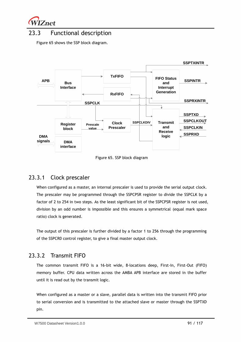
W7500 Datasheet Version1.0.0 91 / 117
Functional description 23.3
Figure 65 shows the SSP block diagram.
Figure 65. SSP block diagram
Clock prescaler 23.3.1
When configured as a master, an internal prescaler is used to provide the serial output clock.
The prescaler may be programmed through the SSPCPSR register to divide the SSPCLK by a
factor of 2 to 254 in two steps. As the least significant bit of the SSPCPSR register is not used,
division by an odd number is impossible and this ensures a symmetrical (equal mark space
ratio) clock is generated.
The output of this prescaler is further divided by a factor 1 to 256 through the programming
of the SSPCR0 control register, to give a final master output clock.
Transmit FIFO 23.3.2
The common transmit FIFO is a 16-bit wide, 8-locations deep, First-In, First-Out (FIFO)
memory buffer. CPU data written across the AMBA APB interface are stored in the buffer
until it is read out by the transmit logic.
When configured as a master or a slave, parallel data is written into the transmit FIFO prior
to serial conversion and is transmitted to the attached slave or master through the SSPTXD
pin.
Register
block
TxFIFO
RxFIFO
FIFO Status
and
Interrupt
Generation
Bus
Interface
Transmit
and
Receive
logic
Clock
Prescaler
SSPINTR
SSPCLK
DMA
interface
SSPTXD
SSPCLKOUT
SSPCLKIN
SSPRXD
Prescale
value
SSPCLKDIV
APB
SSPTXINTR
SSPRXINTR
DMA
signals
W7500 Datasheet Version1.0.0 92 / 117
Receive FIFO 23.3.3
The common receive FIFO is a 16-bit wide, 8-locations deep, first-in, first-out memory buffer.
Received data from the serial interface are stored in the buffer until it is read out by the
CPU across the AMBA APB interface.
When configured as a master or slave, serial data received through the SSPRXD pin is
registered prior to parallel loading into the attached slave or master receive FIFO.
Interrupt generation logic 23.3.4
The PrimeCell SSP generates four individual maskable, active-HIGH interrupts. A combined
interrupt output is also generated as an OR function of the individual interrupt requests.
Users can use the single combined interrupt with a system interrupt controller that provides
another level of masking on a per-peripheral basis. This enables use of modular device
drivers that always know where to find the interrupt source control register bits.
Users can also use the individual interrupt requests with a system interrupt controller that
provides masking for the outputs of each peripheral. In this way, a global interrupt controller
service routine can read the entire set of sources from one wide register in the system
interrupt controller. This is attractive when the time to read from the peripheral registers is
significant compared to the CPU clock speed in a real-time system.
The peripheral supports both methods above.
The transmit and receive dynamic data-flow interrupts, SSPTXINTR and SSPRXINTR, are
separated from the status interrupts so that data can be read or written in response to the
FIFO trigger levels.
DMA interface 23.3.5
The PrimeCell SSP provides an interface to connect to the DMA controller. The PrimeCell SSP
DMA control register, SSPDMACR controls the DMA operation of the PrimeCell SSP.
Receive – The DMA interface includes the following signals for receive:
- SSPRXDMASREQ
Single-character DMA transfer request asserted by the SSP. This signal is
asserted when the receive FIFO contains at least one character.
- SSPRXDMABREQ
W7500 Datasheet Version1.0.0 93 / 117
Burst DMA transfer request, asserted by the SSP. This signal is asserted when
the receive FIFO contains four or more characters.
- SSPRXDMACLR
DMA request clear asserted by the DMA controller to clear the receive
request signals. If DMA burst transfer is requested, the clear signal is
asserted during the transfer of the last data in the burst.
Transmit – The DMA interface includes the following signals for transmit:
- SSPTXDMASREQ
Single-character DMA transfer request asserted by the SSP. This signal is
asserted when there is at least one empty location in the transmit FIFO.
- SSPTXDMABREQ
Burst DMA transfer request asserted by the SSP. This signal is asserted when
the transmit FIFO contains four characters or fewer.
- SSPTXDMACLR
DMA request clear asserted by the DMA controller to clear the transmit
request signals. If a DMA burst transfer is requested, the clear signal is
asserted during the transfer of the last data in the burst.
The burst transfer and single transfer request signals are not mutually exclusive. They can
both be asserted at the same time. For example, when there is more data than the
watermark level of four in the receive FIFO, the burst transfer request and the single
transfer request are asserted.
When the amount of data left in the receive FIFO is less than the watermark level, the single
request only is asserted. This is useful for situations when the number of characters left to
be received in the stream is less than a burst.
For example, if 19 characters must be received, the DMA controller then transfers four
bursts of four characters and three single transfers to complete the stream.
The PrimeCell SSP does not assert the burst request for the remaining three characters.
Each request signal remains asserted until the relevant DMA clear signal is asserted. After
the request clear signal is de-asserted, a request signal can become active again depending
on the conditions that previous sections describe. All request signals are de-asserted if the
PrimeCell SSP is disabled or the DMA enable signal is cleared.
Table 10 shows the trigger points for DMABREQ of both the transmit and receive FIFOs.
Table 10 DMA trigger points for the transmit and receive FIFOs.
Burst length
Watermark Transmit, number of empty locations Receive, number of filled locations
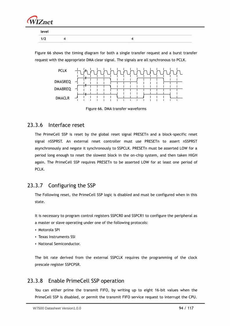
W7500 Datasheet Version1.0.0 94 / 117
level
1/2 4 4
Figure 66 shows the timing diagram for both a single transfer request and a burst transfer
request with the appropriate DMA clear signal. The signals are all synchronous to PCLK.
DMABREQ
DMASREQ
PCLK
DMACLR
Figure 66. DMA transfer waveforms
Interface reset 23.3.6
The PrimeCell SSP is reset by the global reset signal PRESETn and a block-specific reset
signal nSSPRST. An external reset controller must use PRESETn to assert nSSPRST
asynchronously and negate it synchronously to SSPCLK. PRESETn must be asserted LOW for a
period long enough to reset the slowest block in the on-chip system, and then taken HIGH
again. The PrimeCell SSP requires PRESETn to be asserted LOW for at least one period of
PCLK.
Configuring the SSP 23.3.7
The Following reset, the PrimeCell SSP logic is disabled and must be configured when in this
state.
It is necessary to program control registers SSPCR0 and SSPCR1 to configure the peripheral as
a master or slave operating under one of the following protocols:
• Motorola SPI
• Texas Instruments SSI
• National Semiconductor.
The bit rate derived from the external SSPCLK requires the programming of the clock
prescale register SSPCPSR.
Enable PrimeCell SSP operation 23.3.8
You can either prime the transmit FIFO, by writing up to eight 16-bit values when the
PrimeCell SSP is disabled, or permit the transmit FIFO service request to interrupt the CPU.
W7500 Datasheet Version1.0.0 95 / 117
Once enabled, transmission or reception of data begins on the transmit, SSPTXD, and receive,
SSPRXD, pins.
Clock ratios 23.3.9
There is a constraint on the ratio of the frequencies of PCLK to SSPCLK. The frequency of
SSPCLK must be less or equal to that of PCLK. This ensures that control signals from the
SSPCLK domain to the PCLK domain are guaranteed to get synchronized before one frame
duration:
FSSPCLK <= FPCLK.
In the slave mode of operation, the SSPCLKIN signal from the external master is double-
synchronized and then delayed to detect an edge. It takes three SSPCLKs to detect an edge
on SSPCLKIN. SSPTXD has less setup time to the falling edge of SSPCLKIN on which the master
is sampling the line.
The setup and hold times on SSPRXD, with reference to SSPCLKIN, must be more
conservative to ensure that it is at the right value when the actual sampling occurs within
the SSPMS. To ensure correct device operation, SSPCLK must be at least 12 times faster than
the maximum expected frequency of SSPCLKIN.
The frequency selected for SSPCLK must accommodate the desired range of bit clock rates.
The ratio of minimum SSPCLK frequency to SSPCLKOUT maximum frequency in the case of
the slave mode is 12, and for the master mode, it is two.
To generate a maximum bit rate of 1.8432Mbps in the master mode, the frequency of SSPCLK
must be at least 3.6864MHz. With an SSPCLK frequency of 3.6864MHz, the SSPCPSR register
must be programmed with a value of 2, and the SCR[7:0] field in the SSPCR0 register must be
programmed with a value of 0.
To work with a maximum bit rate of 1.8432Mbps in the slave mode, the frequency of SSPCLK
must be at least 22.12MHz. With an SSPCLK frequency of 22.12MHz, the SSPCPSR register can
be programmed with a value of 12 and the SCR[7:0] field in the SSPCR0 register can be
programmed with a value of 0. Similarly, the ratio of SSPCLK maximum frequency to
SSPCLKOUT minimum frequency is 254 x 256.
The minimum frequency of SSPCLK is calculated by the following equations, both of which
must be satisfied:
FSSPCLK(min) => 2 x FSSPCLKOUT(max), for master mode
FSSPCLK(min) => 12 x FSSPCLKIN(max), for slave mode.
W7500 Datasheet Version1.0.0 96 / 117
The maximum frequency of SSPCLK is calculated by the following equations, both of which
must be satisfied:
FSSPCLK(max) <= 254 x 256 x FSSPCLKOUT(min), for master mode
FSSPCLK(max) <= 254 x 256 x FSSPCLKIN(min), for slave mode.
Programming the SSPCR0 Control Register 23.3.10
The SSPCR0 register is used to:
• program the serial clock rate
• select one of the three protocols
• select the data word size, where applicable.
The Serial Clock Rate (SCR) value in conjunction with the SSPCPSR clock prescale divisor
value, CPSDVSR, is used to derive the PrimeCell SSP transmit and receive bit rate from the
external SSPCLK.
The frame format is programmed through the FRF bits and the data word size through the
DSS bits.
Bit phase and polarity applicable to Motorola SPI format only are programmed through the
SPH and SPO bits.
Programming the SSPCR1 Control Register 23.3.11
The SSPCR1 register is used to:
• select master or slave mode
• enable a loop back test feature
• enable the PrimeCell SSP peripheral.
To configure the PrimeCell SSP as a master, clear the SSPCR1 register master or slave
selection bit, MS, to 0. This is the default value on reset.
Setting the SSPCR1 register MS bit to 1 configures the PrimeCell SSP as a slave. When
configured as a slave, enabling or disabling of the PrimeCell SSP SSPTXD signal is provided
through the SSPCR1 slave mode SSPTXD output disable bit, SOD. You can use this in some
multi-slave environments where masters might parallel broadcast.
Set the Synchronous Serial Port Enable (SSE) bit to 1 to enable the operation of the PrimeCell
SSP.
W7500 Datasheet Version1.0.0 97 / 117
Bit rate generation
The serial bit rate is derived by dividing down the input clock SSPCLK. The clock is first
divided by an even prescale value CPSDVSR in the range of 2-254, and is programmed in
SSPCPSR. The clock is divided again by a value in the range of 1-256, that is 1 + SCR, where
SCR is the value programmed in SSPCR0.
The following equation defines the frequency of the output signal bit clock, SSPCLKOUT:
FSSPCLKOUT =FSSPCLK
CPSDVR × (1 + SCR)
For example, if SSPCLK is 3.6864MHz, and CPSDVSR = 2, then SSPCLKOUT has a
frequency range of 7.2kHz-1.8432MHz.
Frame format 23.3.12
Each data frame is between 4-16 bits long depending on the size of data programmed and is
transmitted starting with the MSB. Users can select the following basic frame types:
• Texas Instruments synchronous serial
• Motorola SPI
• National Semiconductor Microwire.
For all formats, the serial clock SSPCLKOUT is held inactive while the PrimeCell SSP is idle
and transitions at the programmed frequency only during active transmission or reception of
data. The idle state of SSPCLKOUT is utilized to provide a receive timeout indication that
occurs when the receive FIFO still contains data after a timeout period.
For Motorola SPI and National Semiconductor Microwire frame formats, the serial frame
SSPFSSOUT pin is active-LOW and is asserted and pulled-down during the entire transmission
of the frame.
For Texas Instruments synchronous serial frame format, the SSPFSSOUT pin is pulsed for one
serial clock period starting at its rising edge prior to the transmission of each frame. For this
frame format, both the PrimeCell SSP and the off-chip slave device drive their output data
on the rising edge of SSPCLKOUT and latch data from the other device on the falling edge.
Unlike the full-duplex transmission of the other two frame formats, the National
Semiconductor Microwire format uses a special master-slave messaging technique which
operates at half-duplex. In this mode, an 8-bit control message is transmitted to the off-chip
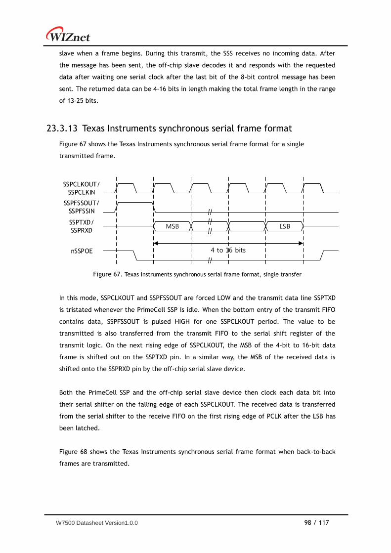
W7500 Datasheet Version1.0.0 98 / 117
slave when a frame begins. During this transmit, the SSS receives no incoming data. After
the message has been sent, the off-chip slave decodes it and responds with the requested
data after waiting one serial clock after the last bit of the 8-bit control message has been
sent. The returned data can be 4-16 bits in length making the total frame length in the range
of 13-25 bits.
Texas Instruments synchronous serial frame format 23.3.13
Figure 67 shows the Texas Instruments synchronous serial frame format for a single
transmitted frame.
SSPFSSOUT/
SSPFSSIN
SSPTXD/
SSPRXD
4 to 16 bits
SSPCLKOUT/
SSPCLKIN
MSB LSB
nSSPOE
Figure 67. Texas Instruments synchronous serial frame format, single transfer
In this mode, SSPCLKOUT and SSPFSSOUT are forced LOW and the transmit data line SSPTXD
is tristated whenever the PrimeCell SSP is idle. When the bottom entry of the transmit FIFO
contains data, SSPFSSOUT is pulsed HIGH for one SSPCLKOUT period. The value to be
transmitted is also transferred from the transmit FIFO to the serial shift register of the
transmit logic. On the next rising edge of SSPCLKOUT, the MSB of the 4-bit to 16-bit data
frame is shifted out on the SSPTXD pin. In a similar way, the MSB of the received data is
shifted onto the SSPRXD pin by the off-chip serial slave device.
Both the PrimeCell SSP and the off-chip serial slave device then clock each data bit into
their serial shifter on the falling edge of each SSPCLKOUT. The received data is transferred
from the serial shifter to the receive FIFO on the first rising edge of PCLK after the LSB has
been latched.
Figure 68 shows the Texas Instruments synchronous serial frame format when back-to-back
frames are transmitted.
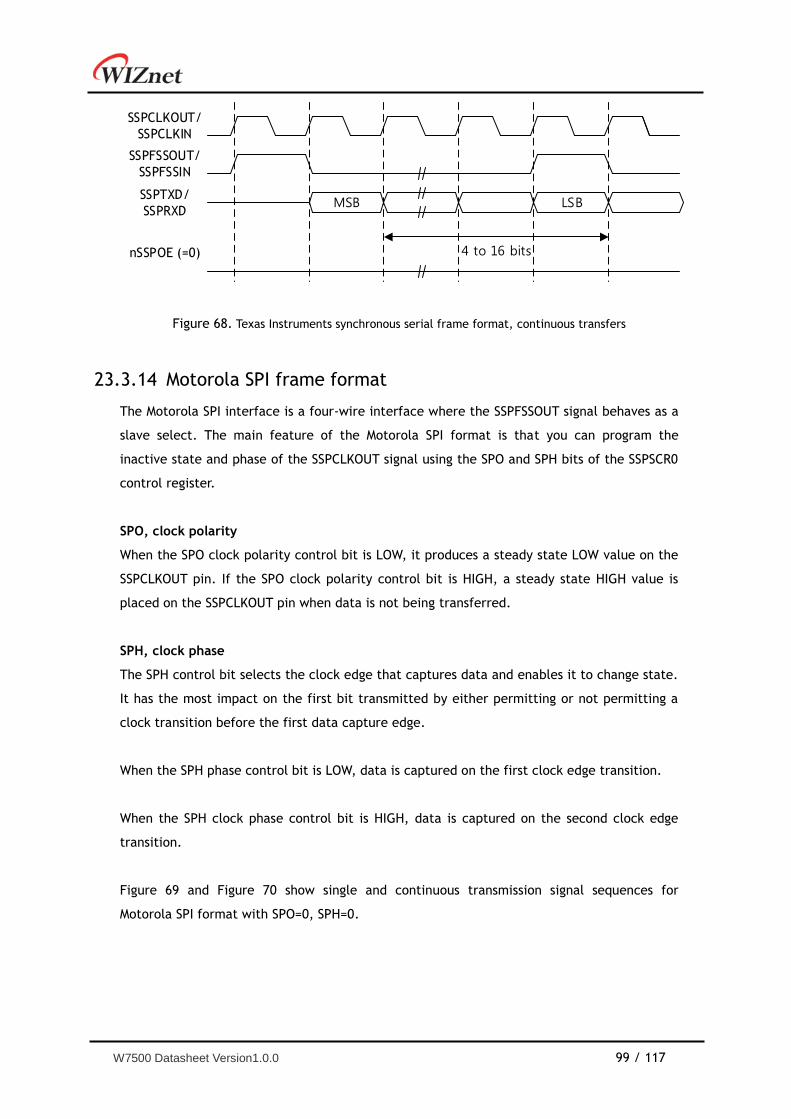
W7500 Datasheet Version1.0.0 99 / 117
SSPFSSOUT/
SSPFSSIN
SSPTXD/
SSPRXD
4 to 16 bits
SSPCLKOUT/
SSPCLKIN
MSB LSB
nSSPOE (=0)
Figure 68. Texas Instruments synchronous serial frame format, continuous transfers
Motorola SPI frame format 23.3.14
The Motorola SPI interface is a four-wire interface where the SSPFSSOUT signal behaves as a
slave select. The main feature of the Motorola SPI format is that you can program the
inactive state and phase of the SSPCLKOUT signal using the SPO and SPH bits of the SSPSCR0
control register.
SPO, clock polarity
When the SPO clock polarity control bit is LOW, it produces a steady state LOW value on the
SSPCLKOUT pin. If the SPO clock polarity control bit is HIGH, a steady state HIGH value is
placed on the SSPCLKOUT pin when data is not being transferred.
SPH, clock phase
The SPH control bit selects the clock edge that captures data and enables it to change state.
It has the most impact on the first bit transmitted by either permitting or not permitting a
clock transition before the first data capture edge.
When the SPH phase control bit is LOW, data is captured on the first clock edge transition.
When the SPH clock phase control bit is HIGH, data is captured on the second clock edge
transition.
Figure 69 and Figure 70 show single and continuous transmission signal sequences for
Motorola SPI format with SPO=0, SPH=0.
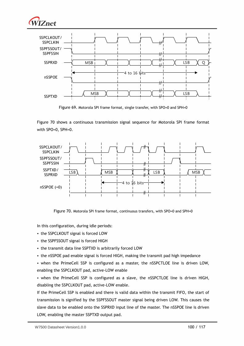
W7500 Datasheet Version1.0.0 100 / 117
SSPFSSOUT/
SSPFSSIN
SSPRXD
4 to 16 bits
SSPCLKOUT/
SSPCLKIN
LSB
nSSPOE
MSB
LSBMSB
MSB LSB
LSB Q
SSPTXD
Figure 69. Motorola SPI frame format, single transfer, with SPO=0 and SPH=0
Figure 70 shows a continuous transmission signal sequence for Motorola SPI frame format
with SPO=0, SPH=0.
SSPFSSOUT/
SSPFSSIN
SSPTXD/
SSPRXD
4 to 16 bits
SSPCLKOUT/
SSPCLKIN
LSB
nSSPOE (=0)
LSBMSBLSB MSB
Figure 70. Motorola SPI frame format, continuous transfers, with SPO=0 and SPH=0
In this configuration, during idle periods:
• the SSPCLKOUT signal is forced LOW
• the SSPFSSOUT signal is forced HIGH
• the transmit data line SSPTXD is arbitrarily forced LOW
• the nSSPOE pad enable signal is forced HIGH, making the transmit pad high impedance
• when the PrimeCell SSP is configured as a master, the nSSPCTLOE line is driven LOW,
enabling the SSPCLKOUT pad, active-LOW enable
• when the PrimeCell SSP is configured as a slave, the nSSPCTLOE line is driven HIGH,
disabling the SSPCLKOUT pad, active-LOW enable.
If the PrimeCell SSP is enabled and there is valid data within the transmit FIFO, the start of
transmission is signified by the SSPFSSOUT master signal being driven LOW. This causes the
slave data to be enabled onto the SSPRXD input line of the master. The nSSPOE line is driven
LOW, enabling the master SSPTXD output pad.
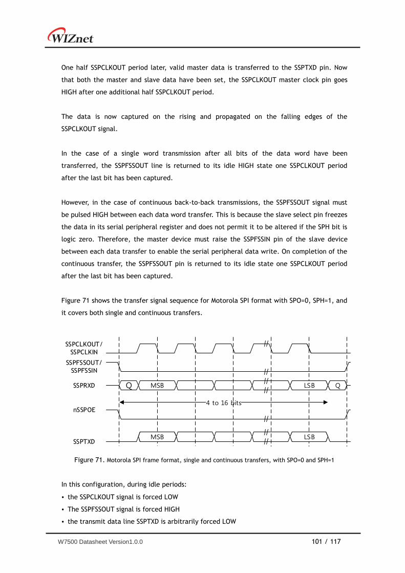
W7500 Datasheet Version1.0.0 101 / 117
One half SSPCLKOUT period later, valid master data is transferred to the SSPTXD pin. Now
that both the master and slave data have been set, the SSPCLKOUT master clock pin goes
HIGH after one additional half SSPCLKOUT period.
The data is now captured on the rising and propagated on the falling edges of the
SSPCLKOUT signal.
In the case of a single word transmission after all bits of the data word have been
transferred, the SSPFSSOUT line is returned to its idle HIGH state one SSPCLKOUT period
after the last bit has been captured.
However, in the case of continuous back-to-back transmissions, the SSPFSSOUT signal must
be pulsed HIGH between each data word transfer. This is because the slave select pin freezes
the data in its serial peripheral register and does not permit it to be altered if the SPH bit is
logic zero. Therefore, the master device must raise the SSPFSSIN pin of the slave device
between each data transfer to enable the serial peripheral data write. On completion of the
continuous transfer, the SSPFSSOUT pin is returned to its idle state one SSPCLKOUT period
after the last bit has been captured.
Figure 71 shows the transfer signal sequence for Motorola SPI format with SPO=0, SPH=1, and
it covers both single and continuous transfers.
SSPFSSOUT/
SSPFSSIN
SSPRXD
4 to 16 bits
SSPCLKOUT/
SSPCLKIN
LSB
nSSPOE
LSBMSB
MSB LSB
LSB Q
SSPTXD
Q MSB
Figure 71. Motorola SPI frame format, single and continuous transfers, with SPO=0 and SPH=1
In this configuration, during idle periods:
• the SSPCLKOUT signal is forced LOW
• The SSPFSSOUT signal is forced HIGH
• the transmit data line SSPTXD is arbitrarily forced LOW
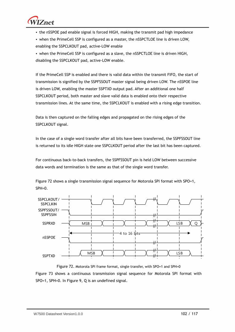
W7500 Datasheet Version1.0.0 102 / 117
• the nSSPOE pad enable signal is forced HIGH, making the transmit pad high impedance
• when the PrimeCell SSP is configured as a master, the nSSPCTLOE line is driven LOW,
enabling the SSPCLKOUT pad, active-LOW enable
• when the PrimeCell SSP is configured as a slave, the nSSPCTLOE line is driven HIGH,
disabling the SSPCLKOUT pad, active-LOW enable.
If the PrimeCell SSP is enabled and there is valid data within the transmit FIFO, the start of
transmission is signified by the SSPFSSOUT master signal being driven LOW. The nSSPOE line
is driven LOW, enabling the master SSPTXD output pad. After an additional one half
SSPCLKOUT period, both master and slave valid data is enabled onto their respective
transmission lines. At the same time, the SSPCLKOUT is enabled with a rising edge transition.
Data is then captured on the falling edges and propagated on the rising edges of the
SSPCLKOUT signal.
In the case of a single word transfer after all bits have been transferred, the SSPFSSOUT line
is returned to its idle HIGH state one SSPCLKOUT period after the last bit has been captured.
For continuous back-to-back transfers, the SSPFSSOUT pin is held LOW between successive
data words and termination is the same as that of the single word transfer.
Figure 72 shows a single transmission signal sequence for Motorola SPI format with SPO=1,
SPH=0.
SSPFSSOUT/
SSPFSSIN
SSPRXD
4 to 16 bits
SSPCLKOUT/
SSPCLKIN
LSB
nSSPOE
MSB
LSBMSB
MSB LSB
LSB Q
SSPTXD
Figure 72. Motorola SPI frame format, single transfer, with SPO=1 and SPH=0
Figure 73 shows a continuous transmission signal sequence for Motorola SPI format with
SPO=1, SPH=0. In Figure 9, Q is an undefined signal.
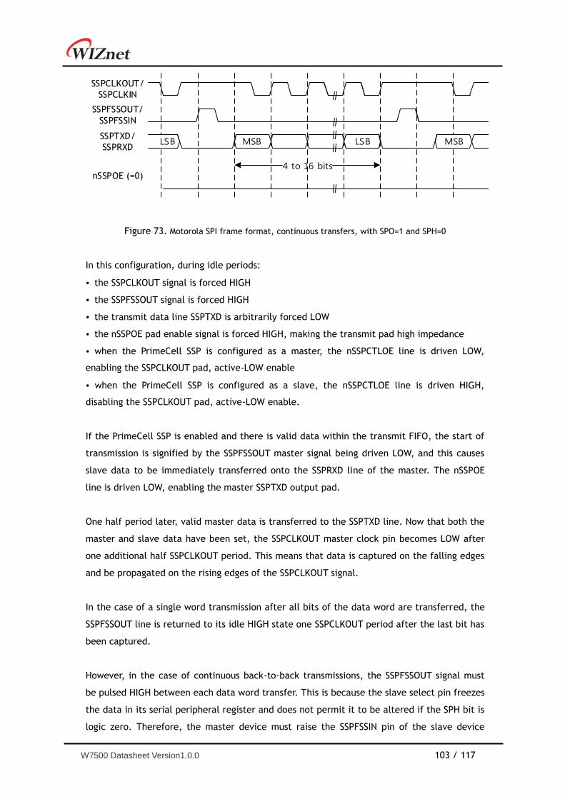
W7500 Datasheet Version1.0.0 103 / 117
SSPFSSOUT/
SSPFSSIN
SSPTXD/
SSPRXD
4 to 16 bits
SSPCLKOUT/
SSPCLKIN
LSB
nSSPOE (=0)
LSBMSBLSB MSB
Figure 73. Motorola SPI frame format, continuous transfers, with SPO=1 and SPH=0
In this configuration, during idle periods:
• the SSPCLKOUT signal is forced HIGH
• the SSPFSSOUT signal is forced HIGH
• the transmit data line SSPTXD is arbitrarily forced LOW
• the nSSPOE pad enable signal is forced HIGH, making the transmit pad high impedance
• when the PrimeCell SSP is configured as a master, the nSSPCTLOE line is driven LOW,
enabling the SSPCLKOUT pad, active-LOW enable
• when the PrimeCell SSP is configured as a slave, the nSSPCTLOE line is driven HIGH,
disabling the SSPCLKOUT pad, active-LOW enable.
If the PrimeCell SSP is enabled and there is valid data within the transmit FIFO, the start of
transmission is signified by the SSPFSSOUT master signal being driven LOW, and this causes
slave data to be immediately transferred onto the SSPRXD line of the master. The nSSPOE
line is driven LOW, enabling the master SSPTXD output pad.
One half period later, valid master data is transferred to the SSPTXD line. Now that both the
master and slave data have been set, the SSPCLKOUT master clock pin becomes LOW after
one additional half SSPCLKOUT period. This means that data is captured on the falling edges
and be propagated on the rising edges of the SSPCLKOUT signal.
In the case of a single word transmission after all bits of the data word are transferred, the
SSPFSSOUT line is returned to its idle HIGH state one SSPCLKOUT period after the last bit has
been captured.
However, in the case of continuous back-to-back transmissions, the SSPFSSOUT signal must
be pulsed HIGH between each data word transfer. This is because the slave select pin freezes
the data in its serial peripheral register and does not permit it to be altered if the SPH bit is
logic zero. Therefore, the master device must raise the SSPFSSIN pin of the slave device
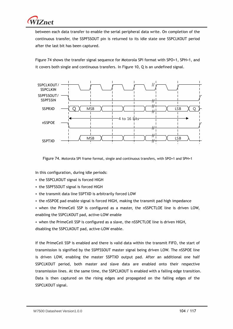
W7500 Datasheet Version1.0.0 104 / 117
between each data transfer to enable the serial peripheral data write. On completion of the
continuous transfer, the SSPFSSOUT pin is returned to its idle state one SSPCLKOUT period
after the last bit has been captured.
Figure 74 shows the transfer signal sequence for Motorola SPI format with SPO=1, SPH=1, and
it covers both single and continuous transfers. In Figure 10, Q is an undefined signal.
SSPFSSOUT/
SSPFSSIN
SSPRXD
4 to 16 bits
SSPCLKOUT/
SSPCLKIN
LSB
nSSPOE
LSBMSB
MSB LSB
LSB Q
SSPTXD
Q MSB
Figure 74. Motorola SPI frame format, single and continuous transfers, with SPO=1 and SPH=1
In this configuration, during idle periods:
• the SSPCLKOUT signal is forced HIGH
• the SSPFSSOUT signal is forced HIGH
• the transmit data line SSPTXD is arbitrarily forced LOW
• the nSSPOE pad enable signal is forced HIGH, making the transmit pad high impedance
• when the PrimeCell SSP is configured as a master, the nSSPCTLOE line is driven LOW,
enabling the SSPCLKOUT pad, active-LOW enable
• when the PrimeCell SSP is configured as a slave, the nSSPCTLOE line is driven HIGH,
disabling the SSPCLKOUT pad, active-LOW enable.
If the PrimeCell SSP is enabled and there is valid data within the transmit FIFO, the start of
transmission is signified by the SSPFSSOUT master signal being driven LOW. The nSSPOE line
is driven LOW, enabling the master SSPTXD output pad. After an additional one half
SSPCLKOUT period, both master and slave data are enabled onto their respective
transmission lines. At the same time, the SSPCLKOUT is enabled with a falling edge transition.
Data is then captured on the rising edges and propagated on the falling edges of the
SSPCLKOUT signal.
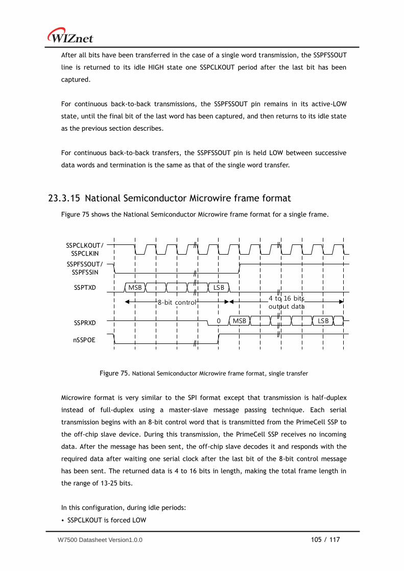
W7500 Datasheet Version1.0.0 105 / 117
After all bits have been transferred in the case of a single word transmission, the SSPFSSOUT
line is returned to its idle HIGH state one SSPCLKOUT period after the last bit has been
captured.
For continuous back-to-back transmissions, the SSPFSSOUT pin remains in its active-LOW
state, until the final bit of the last word has been captured, and then returns to its idle state
as the previous section describes.
For continuous back-to-back transfers, the SSPFSSOUT pin is held LOW between successive
data words and termination is the same as that of the single word transfer.
National Semiconductor Microwire frame format 23.3.15
Figure 75 shows the National Semiconductor Microwire frame format for a single frame.
SSPFSSOUT/
SSPFSSIN
SSPTXD
4 to 16 bitsoutput data
SSPCLKOUT/
SSPCLKIN
LSB
nSSPOE
LSB
0 LSBMSB
MSB LSBSSPRXD
8-bit control
LSB
MSB
Figure 75. National Semiconductor Microwire frame format, single transfer
Microwire format is very similar to the SPI format except that transmission is half-duplex
instead of full-duplex using a master-slave message passing technique. Each serial
transmission begins with an 8-bit control word that is transmitted from the PrimeCell SSP to
the off-chip slave device. During this transmission, the PrimeCell SSP receives no incoming
data. After the message has been sent, the off-chip slave decodes it and responds with the
required data after waiting one serial clock after the last bit of the 8-bit control message
has been sent. The returned data is 4 to 16 bits in length, making the total frame length in
the range of 13-25 bits.
In this configuration, during idle periods:
• SSPCLKOUT is forced LOW
W7500 Datasheet Version1.0.0 106 / 117
• SSPFSSOUT is forced HIGH
• the transmit data line, SSPTXD, is arbitrarily forced LOW
• the nSSPOE pad enable signal is forced HIGH, making the transmit pad high impedance.
A transmission is triggered by writing a control byte to the transmit FIFO. The falling edge of
SSPFSSOUT causes the value contained in the bottom entry of the transmit FIFO to be
transferred to the serial shift register of the transmit logic and the MSB of the 8-bit control
frame to be shifted out onto the SSPTXD pin. SSPFSSOUT remains LOW for the duration of
the frame transmission. The SSPRXD pin remains tristated during this transmission.
The off-chip serial slave device latches each control bit into its serial shifter on the rising
edge of each SSPCLKOUT. After the last bit is latched by the slave device, the control byte is
decoded during a one clock wait-state and the slave responds by transmitting data back to
the PrimeCell SSP. Each bit is driven onto the SSPRXD line on the falling edge of SSPCLKOUT.
The PrimeCell SSP in turn latches each bit on the rising edge of SSPCLKOUT. At the end of the
frame for single transfers, the SSPFSSOUT signal is pulled HIGH one clock period after the
last bit has been latched in the receive serial shifter, which causes the data to be
transferred to the receive FIFO.
The off-chip slave device can tristate the receive line either on the falling edge of
SSPCLKOUT after the LSB has been latched by the receive shifter or when the SSPFSSOUT pin
goes HIGH.
For continuous transfers, data transmission begins and ends in the same manner as a single
transfer. However, the SSPFSSOUT line is continuously asserted, held LOW, and transmission
of data occurs back-to-back. The control byte of the next frame follows directly after the
LSB of the received data from the current frame. Each of the received values is transferred
from the receive shifter on the falling edge SSPCLKOUT, after the LSB of the frame has been
latched into the PrimeCell SSP.
Figure 76 shows the National Semiconductor Microwire frame format when back-to-back
frames are transmitted.
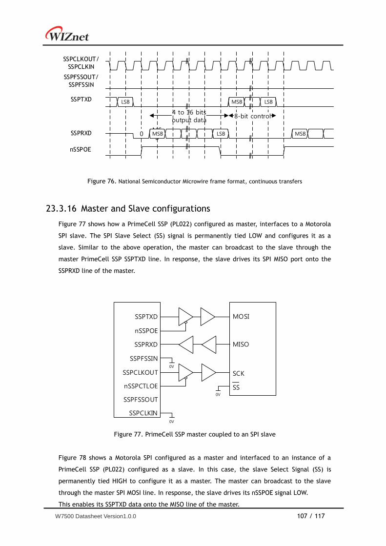
W7500 Datasheet Version1.0.0 107 / 117
SSPFSSOUT/
SSPFSSIN
SSPTXD
4 to 16 bitsoutput data
SSPCLKOUT/
SSPCLKIN
LSB
nSSPOE
LSB
0 LSBMSB
MSB LSBSSPRXD
8-bit control
LSB
MSB LSB
MSB
Figure 76. National Semiconductor Microwire frame format, continuous transfers
Master and Slave configurations 23.3.16
Figure 77 shows how a PrimeCell SSP (PL022) configured as master, interfaces to a Motorola
SPI slave. The SPI Slave Select (SS) signal is permanently tied LOW and configures it as a
slave. Similar to the above operation, the master can broadcast to the slave through the
master PrimeCell SSP SSPTXD line. In response, the slave drives its SPI MISO port onto the
SSPRXD line of the master.
0V
0V
0V
SSPTXD
nSSPOE
SSPRXD
SSPFSSIN
SSPCLKOUT
nSSPCTLOE
SSPCLKIN
MOSI
SCK
MISO
SS
SSPFSSOUT
Figure 77. PrimeCell SSP master coupled to an SPI slave
Figure 78 shows a Motorola SPI configured as a master and interfaced to an instance of a
PrimeCell SSP (PL022) configured as a slave. In this case, the slave Select Signal (SS) is
permanently tied HIGH to configure it as a master. The master can broadcast to the slave
through the master SPI MOSI line. In response, the slave drives its nSSPOE signal LOW.
This enables its SSPTXD data onto the MISO line of the master.
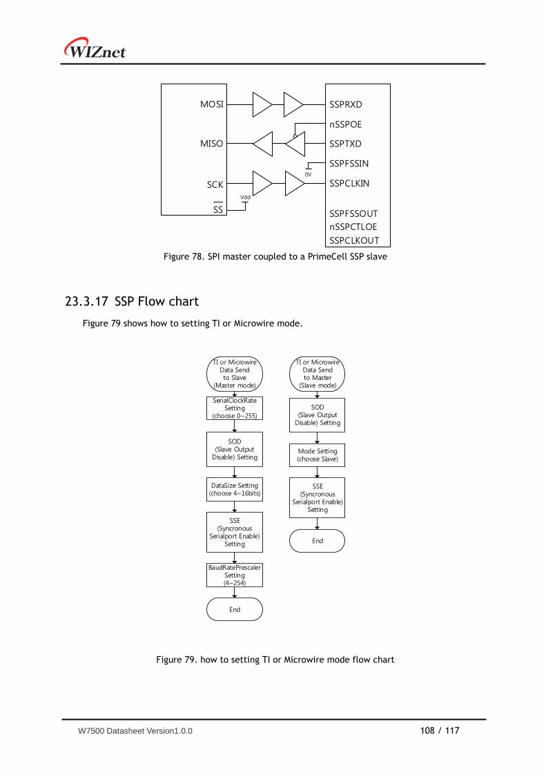
W7500 Datasheet Version1.0.0 108 / 117
Vdd
0V
SSPRXD
nSSPOE
SSPTXD
SSPFSSIN
SSPCLKIN
nSSPCTLOE
SSPCLKOUT
MOSI
SCK
MISO
SS SSPFSSOUT
Figure 78. SPI master coupled to a PrimeCell SSP slave
SSP Flow chart 23.3.17
Figure 79 shows how to setting TI or Microwire mode.
TI or Microwire Data Send to Slave
(Master mode)
SerialClockRateSetting
(choose 0~255)
DataSize Setting(choose 4~16bits)
SSE(Syncronous
Serialport Enable) Setting
End
BaudRatePrescaler Setting (4~254)
TI or Microwire Data Send to Master
(Slave mode)
Mode Setting(choose Slave)
SSE(Syncronous
Serialport Enable) Setting
End
SOD(Slave Output
Disable) Setting
SOD(Slave Output
Disable) Setting
Figure 79. how to setting TI or Microwire mode flow chart
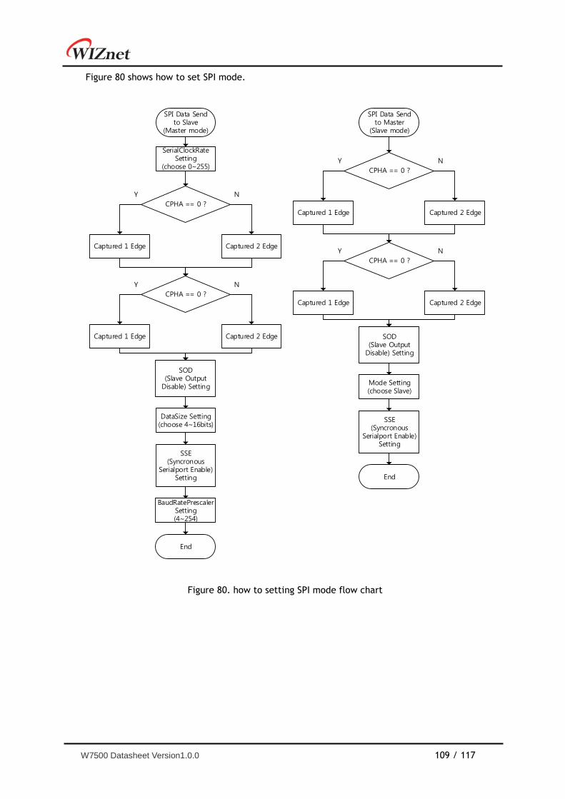
W7500 Datasheet Version1.0.0 109 / 117
Figure 80 shows how to set SPI mode.
SPI Data Send to Slave
(Master mode)
SerialClockRateSetting
(choose 0~255)
Y
CPHA == 0 ?
N
Captured 1 Edge Captured 2 Edge
Y
CPHA == 0 ?
N
Captured 1 Edge Captured 2 Edge
DataSize Setting(choose 4~16bits)
SSE(Syncronous
Serialport Enable) Setting
End
BaudRatePrescaler Setting (4~254)
SPI Data Send to Master
(Slave mode)
Y
CPHA == 0 ?
N
Captured 1 Edge Captured 2 Edge
Y
CPHA == 0 ?
N
Captured 1 Edge Captured 2 Edge
Mode Setting(choose Slave)
SSE(Syncronous
Serialport Enable) Setting
End
SOD(Slave Output
Disable) Setting
SOD(Slave Output
Disable) Setting
Figure 80. how to setting SPI mode flow chart
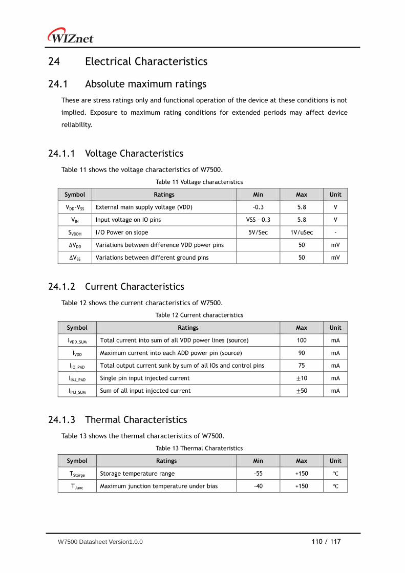
W7500 Datasheet Version1.0.0 110 / 117
24 Electrical Characteristics
Absolute maximum ratings 24.1
These are stress ratings only and functional operation of the device at these conditions is not
implied. Exposure to maximum rating conditions for extended periods may affect device
reliability.
Voltage Characteristics 24.1.1
Table 11 shows the voltage characteristics of W7500.
Table 11 Voltage characteristics
Symbol Ratings Min Max Unit
VDD-VSS External main supply voltage (VDD) -0.3 5.8 V
VIN Input voltage on IO pins VSS – 0.3 5.8 V
SVDDH I/O Power on slope 5V/Sec 1V/uSec -
VDD Variations between difference VDD power pins 50 mV
VSS Variations between different ground pins 50 mV
Current Characteristics 24.1.2
Table 12 shows the current characteristics of W7500.
Table 12 Current characteristics
Symbol Ratings Max Unit
IVDD_SUM Total current into sum of all VDD power lines (source) 100 mA
IVDD Maximum current into each ADD power pin (source) 90 mA
IIO_PAD Total output current sunk by sum of all IOs and control pins 75 mA
IINJ_PAD Single pin input injected current 10 mA
IINJ_SUM Sum of all input injected current 50 mA
Thermal Characteristics 24.1.3
Table 13 shows the thermal characteristics of W7500.
Table 13 Thermal Charateristics
Symbol Ratings Min Max Unit
TStorge Storage temperature range -55 +150
TJunc Maximum junction temperature under bias -40 +150
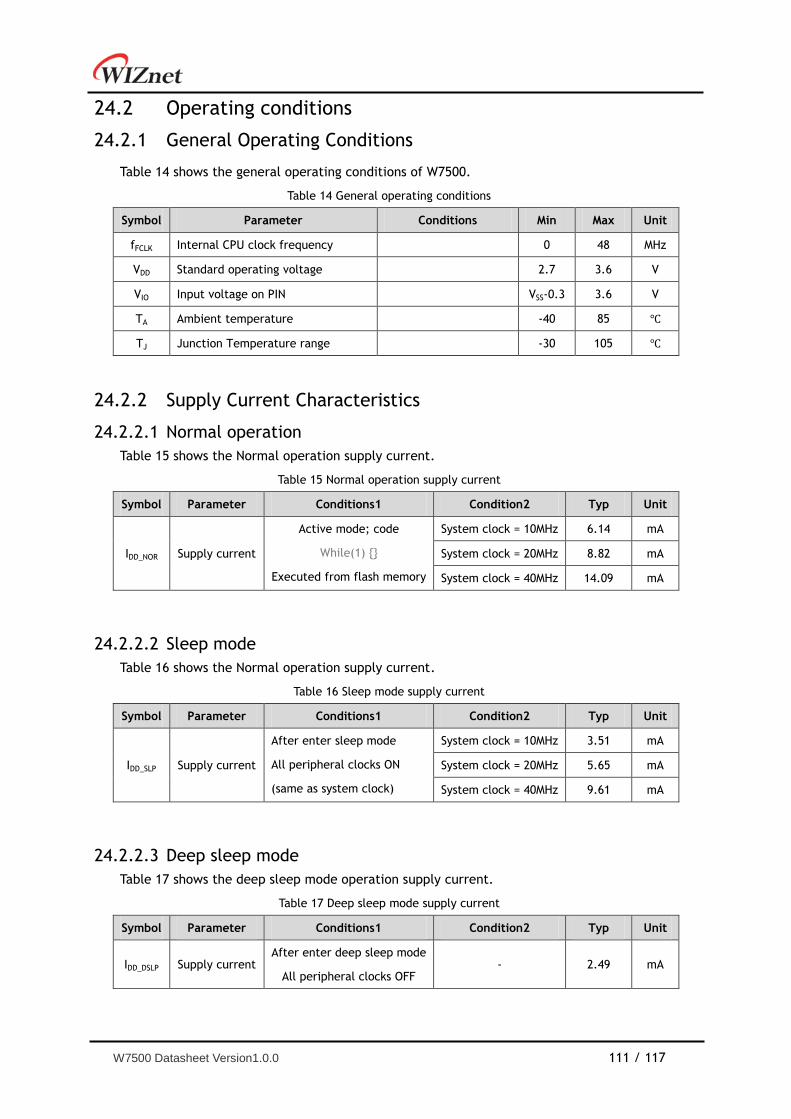
W7500 Datasheet Version1.0.0 111 / 117
Operating conditions 24.2
General Operating Conditions 24.2.1
Table 14 shows the general operating conditions of W7500.
Table 14 General operating conditions
Symbol Parameter Conditions Min Max Unit
fFCLK Internal CPU clock frequency 0 48 MHz
VDD Standard operating voltage 2.7 3.6 V
VIO Input voltage on PIN VSS-0.3 3.6 V
TA Ambient temperature -40 85
TJ Junction Temperature range -30 105
Supply Current Characteristics 24.2.2
24.2.2.1 Normal operation
Table 15 shows the Normal operation supply current.
Table 15 Normal operation supply current
Symbol Parameter Conditions1 Condition2 Typ Unit
IDD_NOR Supply current
Active mode; code
While(1) {}
Executed from flash memory
System clock = 10MHz 6.14 mA
System clock = 20MHz 8.82 mA
System clock = 40MHz 14.09 mA
24.2.2.2 Sleep mode
Table 16 shows the Normal operation supply current.
Table 16 Sleep mode supply current
Symbol Parameter Conditions1 Condition2 Typ Unit
IDD_SLP Supply current
After enter sleep mode
All peripheral clocks ON
(same as system clock)
System clock = 10MHz 3.51 mA
System clock = 20MHz 5.65 mA
System clock = 40MHz 9.61 mA
24.2.2.3 Deep sleep mode
Table 17 shows the deep sleep mode operation supply current.
Table 17 Deep sleep mode supply current
Symbol Parameter Conditions1 Condition2 Typ Unit
IDD_DSLP Supply current After enter deep sleep mode
All peripheral clocks OFF - 2.49 mA
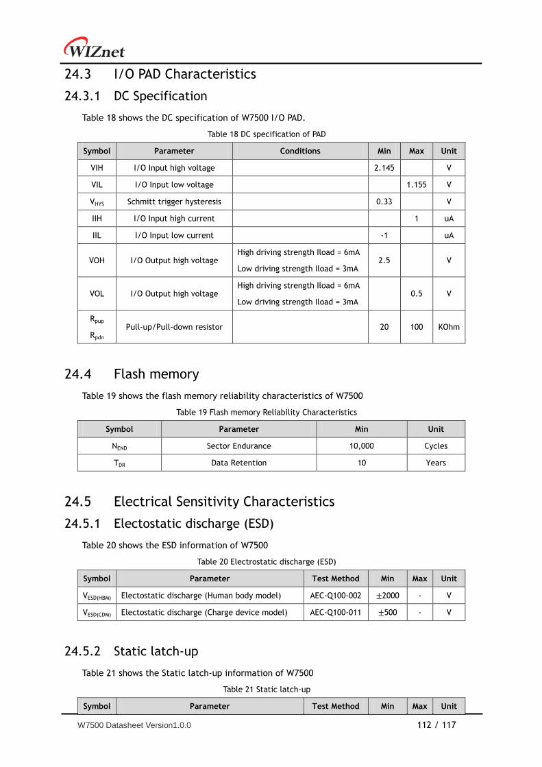
W7500 Datasheet Version1.0.0 112 / 117
I/O PAD Characteristics 24.3
DC Specification 24.3.1
Table 18 shows the DC specification of W7500 I/O PAD.
Table 18 DC specification of PAD
Symbol Parameter Conditions Min Max Unit
VIH I/O Input high voltage 2.145 V
VIL I/O Input low voltage 1.155 V
VHYS Schmitt trigger hysteresis 0.33 V
IIH I/O Input high current 1 uA
IIL I/O Input low current -1 uA
VOH I/O Output high voltage High driving strength Iload = 6mA
Low driving strength Iload = 3mA 2.5 V
VOL I/O Output high voltage High driving strength Iload = 6mA
Low driving strength Iload = 3mA 0.5 V
Rpup
Rpdn Pull-up/Pull-down resistor
20 100 KOhm
Flash memory 24.4
Table 19 shows the flash memory reliability characteristics of W7500
Table 19 Flash memory Reliability Characteristics
Symbol Parameter Min Unit
NEND Sector Endurance 10,000 Cycles
TDR Data Retention 10 Years
Electrical Sensitivity Characteristics 24.5
Electostatic discharge (ESD) 24.5.1
Table 20 shows the ESD information of W7500
Table 20 Electrostatic discharge (ESD)
Symbol Parameter Test Method Min Max Unit
VESD(HBM) Electostatic discharge (Human body model) AEC-Q100-002 2000 - V
VESD(CDM) Electostatic discharge (Charge device model) AEC-Q100-011 500 - V
Static latch-up 24.5.2
Table 21 shows the Static latch-up information of W7500
Table 21 Static latch-up
Symbol Parameter Test Method Min Max Unit
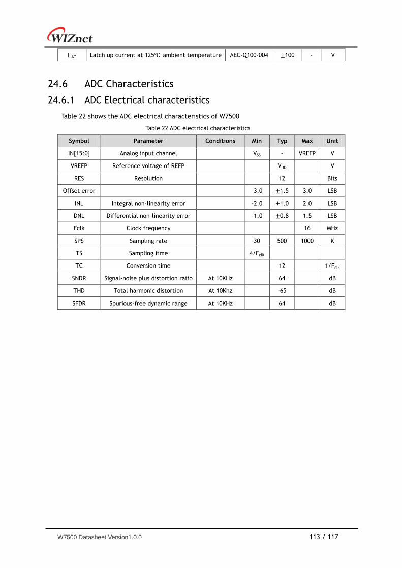
W7500 Datasheet Version1.0.0 113 / 117
ILAT Latch up current at 125 ambient temperature AEC-Q100-004 100 - V
ADC Characteristics 24.6
ADC Electrical characteristics 24.6.1
Table 22 shows the ADC electrical characteristics of W7500
Table 22 ADC electrical characteristics
Symbol Parameter Conditions Min Typ Max Unit
IN[15:0] Analog input channel VSS - VREFP V
VREFP Reference voltage of REFP VDD V
RES Resolution 12 Bits
Offset error -3.0 1.5 3.0 LSB
INL Integral non-linearity error -2.0 1.0 2.0 LSB
DNL Differential non-linearity error -1.0 0.8 1.5 LSB
Fclk Clock frequency 16 MHz
SPS Sampling rate 30 500 1000 K
TS Sampling time 4/Fclk
TC Conversion time 12 1/Fclk
SNDR Signal-noise plus distortion ratio At 10KHz 64 dB
THD Total harmonic distortion At 10Khz -65 dB
SFDR Spurious-free dynamic range At 10KHz 64 dB
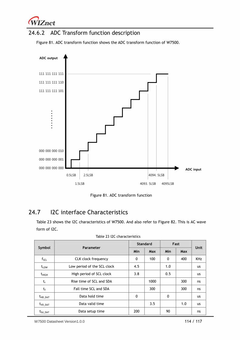
W7500 Datasheet Version1.0.0 114 / 117
ADC Transform function description 24.6.2
Figure 81. ADC transform function shows the ADC transform function of W7500.
4095LSB4093. 5LSB
ADC input
4094. 5LSB0.5LSB 2.5LSB
1.5LSB
000 000 000 000
000 000 000 001
000 000 000 010
111 111 111 101
111 111 111 110
111 111 111 111
ADC output
Figure 81. ADC transform function
I2C interface Characteristics 24.7
Table 23 shows the I2C characteristics of W7500. And also refer to Figure 82. This is AC wave
form of I2C.
Table 23 I2C characteristics
Symbol Parameter Standard Fast
Unit Min Max Min Max
fSCL CLK clock frequency 0 100 0 400 KHz
tLOW Low period of the SCL clock 4.5 1.0 us
tHIGH High period of SCL clock 3.8 0.5 us
tr Rise time of SCL and SDA 1000 300 ns
tf Fall time SCL and SDA 300 300 ns
tHD_DAT Data hold time 0 0 us
tVD_DAT Data valid time 3.5 1.0 us
tSU_DAT Data setup time 200 90 ns
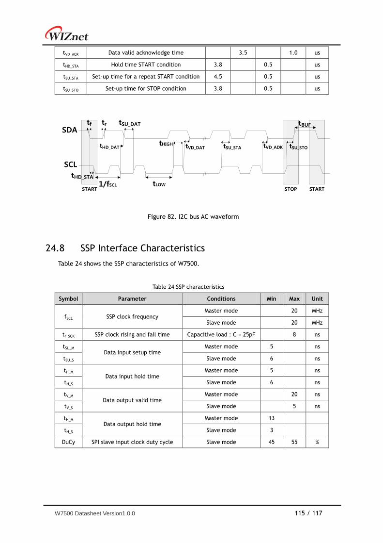
W7500 Datasheet Version1.0.0 115 / 117
tVD_ACK Data valid acknowledge time 3.5 1.0 us
tHD_STA Hold time START condition 3.8 0.5 us
tSU_STA Set-up time for a repeat START condition 4.5 0.5 us
tSU_STO Set-up time for STOP condition 3.8 0.5 us
SDA
SCL
tf tr tSU_DAT
tHD_DAT
tHD_STA
1/fSCL tLOW
tHIGH tVD_DAT tSU_STA tVD_ADK tSU_STO
tBUF
STOP STARTSTART
Figure 82. I2C bus AC waveform
SSP Interface Characteristics 24.8
Table 24 shows the SSP characteristics of W7500.
Table 24 SSP characteristics
Symbol Parameter Conditions Min Max Unit
fSCL SSP clock frequency Master mode 20 MHz
Slave mode 20 MHz
tr_SCK SSP clock rising and fall time Capacitive load : C = 25pF 8 ns
tSU_M Data input setup time
Master mode 5 ns
tSU_S Slave mode 6 ns
tH_M Data input hold time
Master mode 5 ns
tH_S Slave mode 6 ns
tV_M Data output valid time
Master mode 20 ns
tV_S Slave mode 5 ns
tH_M Data output hold time
Master mode 13
tH_S Slave mode 3
DuCy SPI slave input clock duty cycle Slave mode 45 55 %
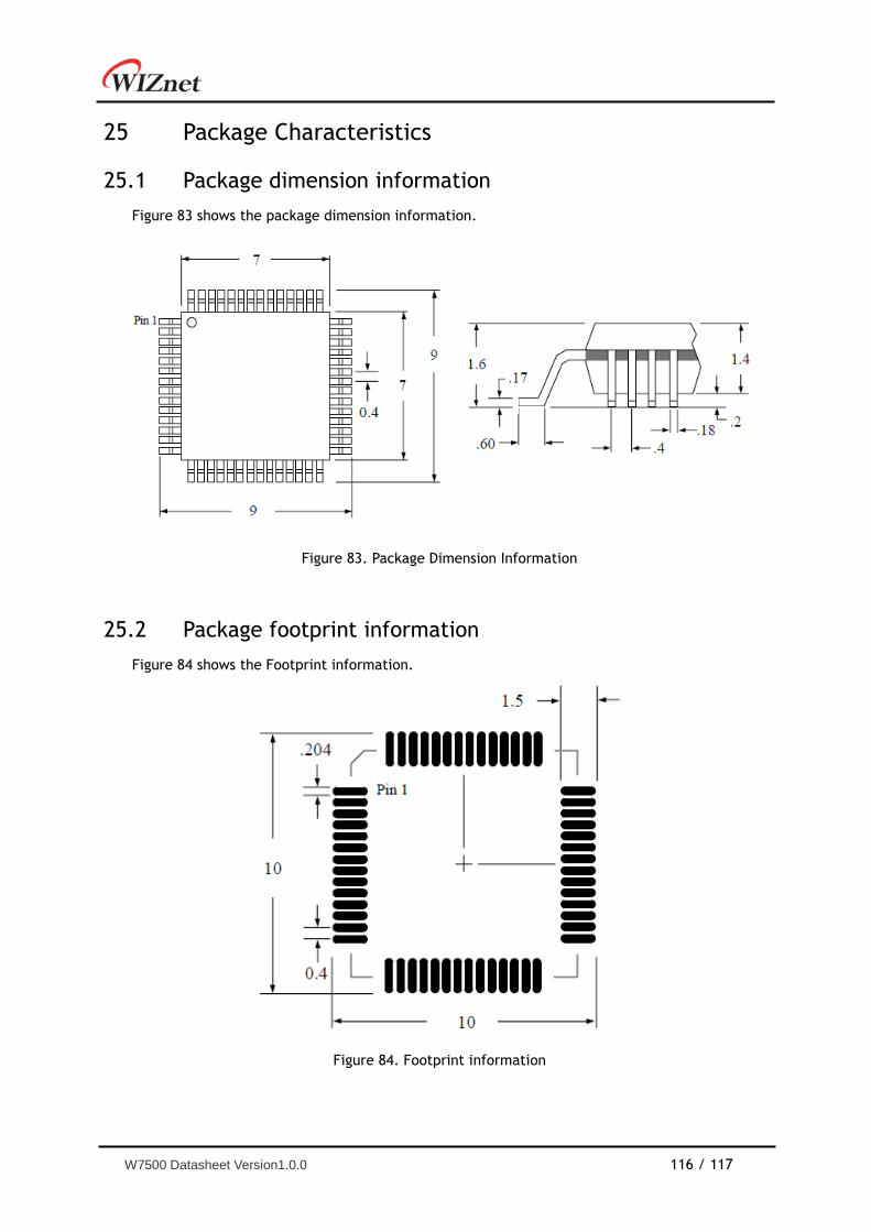
W7500 Datasheet Version1.0.0 116 / 117
25 Package Characteristics
Package dimension information 25.1
Figure 83 shows the package dimension information.
Figure 83. Package Dimension Information
Package footprint information 25.2
Figure 84 shows the Footprint information.
Figure 84. Footprint information

W7500 Datasheet Version1.0.0 117 / 117
Document History Information
Version Date Descriptions
Ver. 1.0.0 01MAY2015 Initial Release
Copyright Notice
Copyright 2015 WIZnet Co., Ltd. All Rights Reserved.
Technical Support: http://wizwiki.net/forum
Sales & Distribution: [email protected]
For more information, visit our website at http://www.wiznet.co.kr