Embed Size (px)
Citation preview
SSPPXX33994400
11AA LLooww DDrrooppoouutt VVoollttaaggee RReegguullaattoorr February 2012 Rev. 1.0.0
Exar Corporation www.exar.com 48720 Kato Road, Fremont CA 94538, USA Tel. +1 510 668-7000 – Fax. +1 510 668-7001
GENERAL DESCRIPTION
The SPX3940 is a 1A, accurate voltage regulator with a low drop out voltage of 280mV (typical) at 1A.
These regulators are specifically designed for low voltage applications that require a low dropout voltage and a fast transient response.
They are fully fault protected against over-current, reverse battery, and positive and negative voltage transients.
The SPX3940 is offered in 3-pin SOT223 and TO-263 packages. For a 3A version, refer to the SPX29300 data sheet.
APPLICATIONS
Power Supplies
LCD Monitors
Portable Instrumentation
Medical and Industrial Equipments
FEATURES
Guaranteed 1.5A Peak Current
1% Output Accuracy SPX3940A
Low Quiescent Current
Low Dropout Voltage of 280mV at 1A
Extremely Tight Load and Line Regulation
Extremely Fast Transient Response
Reverse-battery Protection
Internal Thermal Protection
Internal Short Circuit Current Limit
Replacement for LM3940
Standard SOT223 & TO-263 packages
TYPICAL APPLICATION DIAGRAM
Fig. 1: SPX3940 Application Diagram – Fixed Output Linear Regulator
SSPPXX33994400
11AA LLooww DDrrooppoouutt VVoollttaaggee RReegguullaattoorr
© 2012 Exar Corporation 2/11 Rev. 1.0.0
ABSOLUTE MAXIMUM RATINGS
These are stress ratings only and functional operation of
the device at these ratings or any other above those
indicated in the operation sections of the specifications below is not implied. Exposure to absolute maximum
rating conditions for extended periods of time may affect reliability.
Input Voltage VIN ................................................... 20V1
Storage Temperature .............................. -65°C to 150°C
Lead Temperature (Soldering, 5 sec) ..................... 260°C
OPERATING RATINGS
Input Voltage VIN .................................................... 16V
Junction Temperature Range ....................-40°C to 125°C
Packages Thermal Resistance
SOT-223 Junction to Case (at TA) ..................... 15°C/W
SOT-223 Junction to Ambient ........................62.3°C/W
TO-263 Junction to Case (at TA) ......................... 3°C/W
TO-263 Junction to Ambient ..........................31.4°C/W
Note 1: Maximum positive supply voltage of 20V must be
of limited duration (<100ms) and duty cycle (<1%). The maximum continuous supply voltage is 16V.
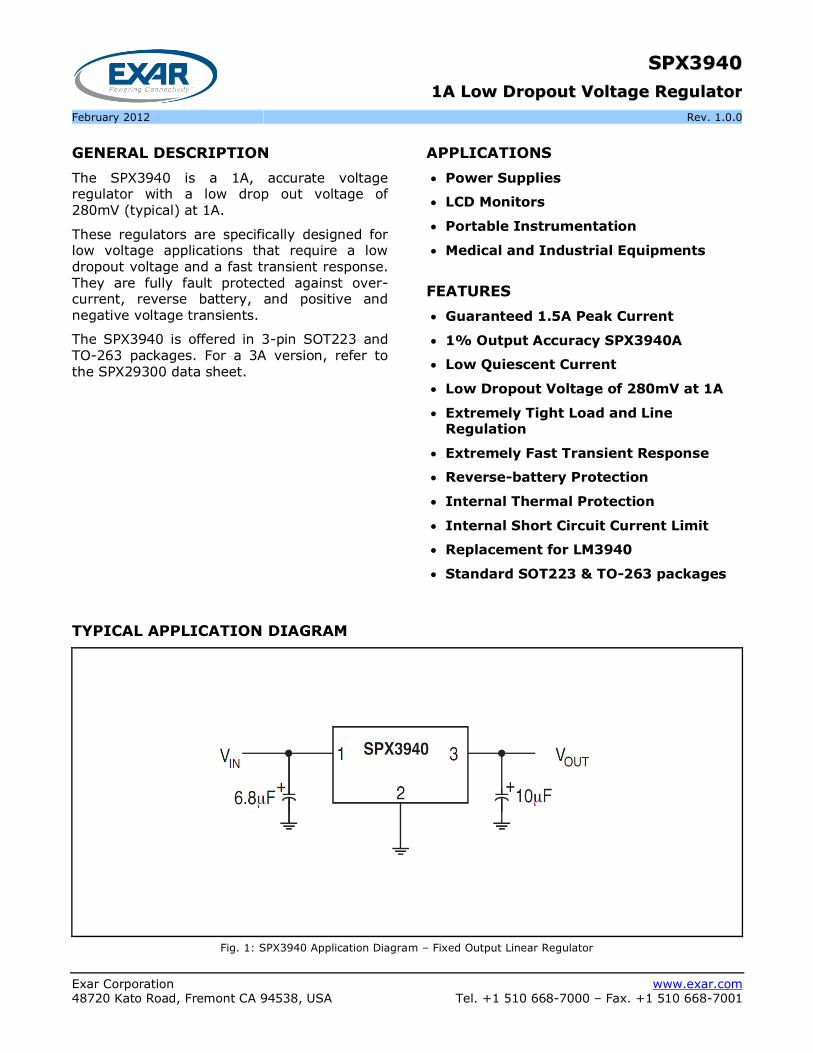
ELECTRICAL SPECIFICATIONS
Specifications with standard type are for an Operating Ambient Temperature of TA = 25°C only; limits applying over the full
Operating Junction Temperature range are denoted by a “•”. Minimum and Maximum limits are guaranteed through test, design, or statistical correlation. Typical values represent the most likely parametric norm at TA = 25°C, and are provided
for reference purposes only. Unless otherwise indicated, VIN = VIN +1V, IOUT = 10mA, CIN = 6.8µF, COUT = 10µF, TA = 25°C.
Parameter Min. Typ. Max. Units Conditions
1.8V version
Output Voltage - SPX3940A (1%) 1.782 1.8 1.818
V
IOUT=10mA 10mA≤IOUT≤1A, 6V≤VIN≤16V
1.755 1.8 1.845 •
Output Voltage - SPX3940 (2%) 1.764 1.8 1.836
V
1.737 1.8 1.863 •
2.5V version
Output Voltage - SPX3940A (1%) 2.475 2.5 2.525
V
IOUT=10mA 10mA≤IOUT≤1A, 6V≤VIN≤16V
2.437 2.5 2.563 •
Output Voltage - SPX3940 (2%) 2.450 2.5 2.550
V
2.412 2.5 2.588 •
3.3V version
Output Voltage - SPX3940A (1%) 3.267 3.3 3.333
V
IOUT=10mA 10mA≤IOUT≤1A, 6V≤VIN≤16V
3.217 3.3 3.383 •
Output Voltage - SPX3940 (2%) 3.234 3.3 3.366
V
3.184 3.3 3.416 •
5.0V version
Output Voltage - SPX3940A (1%) 4.950 5.0 5.050
V
IOUT=10mA
10mA≤IOUT≤1A, 6V≤VIN≤16V
4.875 5.0 5.125 •
Output Voltage - SPX3940 (2%) 4.900 5.0 5.100
V
4.825 5.0 5.175 •
All Voltage Options
Line Regulation 0.2 1.0 % IOUT=10mA, (VOUT +1V)≤VIN≤16V
Load Regulation 0.3 1.5 % VIN = VOUT +1V,10mA≤IOUT≤1A
- Output Voltage
temperature Coefficient 20 100 ppm/°C •
Dropout Voltage2 (except 1.8V version)
70 200 mV • IOUT=100mA
280 550 mV • IOUT=1A
Ground Current3 12 25 mA • IOUT=750mA, VIN = VOUT +1V
18 mA IOUT=1A
IGNDDO Ground Pin Current at
Dropout 1.2 mA VIN = 0.1V less than specified VOUT IOUT=10mA,
Current Limit 1.5 2.2 A VOUT = 0V4
Output Noise Voltage 400 µVRMS 10Hz-100KHz, IL=100mA, CL=10µF
260 µVRMS 10Hz-100KHz, IL=100mA, CL=33µF
SSPPXX33994400
11AA LLooww DDrrooppoouutt VVoollttaaggee RReegguullaattoorr
© 2012 Exar Corporation 3/11 Rev. 1.0.0
Note 2: Dropout voltage is defined as the input to output differential when the output voltage drops to 99% of its normal
value. Note 3: Ground pin current is the regulator quiescent current. The total current drawn from the source is the sum of the
load current to the ground current. Note 4: VIN=VOUT(NOMINAL)+1V. For example, use VIN=4.3V for a 3.3V regulator. Employ pulse-testing procedures to minimize
temperature rise.
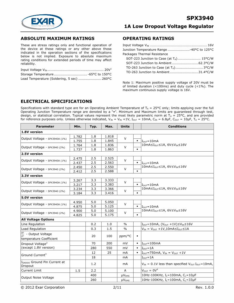
BLOCK DIAGRAM
Fig. 2: SPX3940 Block Diagram
PIN ASSIGNMENT
Fig. 3: SPX3940 Pin Assignment
SSPPXX33994400
11AA LLooww DDrrooppoouutt VVoollttaaggee RReegguullaattoorr
© 2012 Exar Corporation 4/11 Rev. 1.0.0
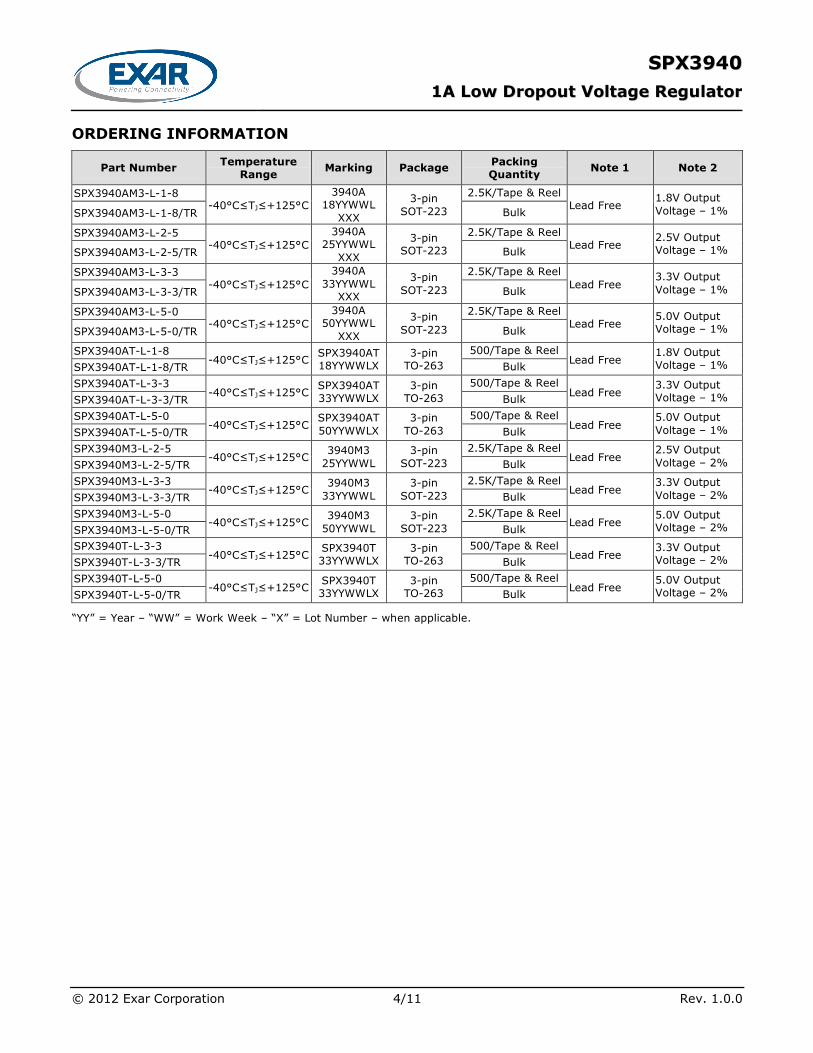
ORDERING INFORMATION
Part Number Temperature
Range Marking Package
Packing
Quantity Note 1 Note 2
SPX3940AM3-L-1-8 -40°C≤TJ≤+125°C
3940A 18YYWWL
XXX
3-pin
SOT-223
2.5K/Tape & Reel Lead Free
1.8V Output
Voltage – 1% SPX3940AM3-L-1-8/TR Bulk
SPX3940AM3-L-2-5 -40°C≤TJ≤+125°C
3940A 25YYWWL
XXX
3-pin SOT-223
2.5K/Tape & Reel Lead Free
2.5V Output Voltage – 1% SPX3940AM3-L-2-5/TR Bulk
SPX3940AM3-L-3-3 -40°C≤TJ≤+125°C
3940A
33YYWWL XXX
3-pin
SOT-223
2.5K/Tape & Reel
Lead Free 3.3V Output
Voltage – 1% SPX3940AM3-L-3-3/TR Bulk
SPX3940AM3-L-5-0 -40°C≤TJ≤+125°C
3940A 50YYWWL
XXX
3-pin
SOT-223
2.5K/Tape & Reel Lead Free
5.0V Output Voltage – 1% SPX3940AM3-L-5-0/TR Bulk
SPX3940AT-L-1-8 -40°C≤TJ≤+125°C
SPX3940AT 18YYWWLX
3-pin TO-263
500/Tape & Reel Lead Free
1.8V Output Voltage – 1% SPX3940AT-L-1-8/TR Bulk
SPX3940AT-L-3-3 -40°C≤TJ≤+125°C
SPX3940AT
33YYWWLX
3-pin
TO-263
500/Tape & Reel Lead Free
3.3V Output
Voltage – 1% SPX3940AT-L-3-3/TR Bulk
SPX3940AT-L-5-0 -40°C≤TJ≤+125°C
SPX3940AT
50YYWWLX
3-pin
TO-263
500/Tape & Reel Lead Free
5.0V Output
Voltage – 1% SPX3940AT-L-5-0/TR Bulk
SPX3940M3-L-2-5 -40°C≤TJ≤+125°C
3940M3
25YYWWL
3-pin
SOT-223
2.5K/Tape & Reel Lead Free
2.5V Output
Voltage – 2% SPX3940M3-L-2-5/TR Bulk
SPX3940M3-L-3-3 -40°C≤TJ≤+125°C
3940M3
33YYWWL
3-pin
SOT-223
2.5K/Tape & Reel Lead Free
3.3V Output
Voltage – 2% SPX3940M3-L-3-3/TR Bulk
SPX3940M3-L-5-0 -40°C≤TJ≤+125°C
3940M3
50YYWWL
3-pin
SOT-223
2.5K/Tape & Reel Lead Free
5.0V Output Voltage – 2% SPX3940M3-L-5-0/TR Bulk
SPX3940T-L-3-3 -40°C≤TJ≤+125°C
SPX3940T 33YYWWLX
3-pin TO-263
500/Tape & Reel Lead Free
3.3V Output Voltage – 2% SPX3940T-L-3-3/TR Bulk
SPX3940T-L-5-0 -40°C≤TJ≤+125°C
SPX3940T 33YYWWLX
3-pin TO-263
500/Tape & Reel Lead Free
5.0V Output Voltage – 2% SPX3940T-L-5-0/TR Bulk
“YY” = Year – “WW” = Work Week – “X” = Lot Number – when applicable.
SSPPXX33994400
11AA LLooww DDrrooppoouutt VVoollttaaggee RReegguullaattoorr
© 2012 Exar Corporation 5/11 Rev. 1.0.0
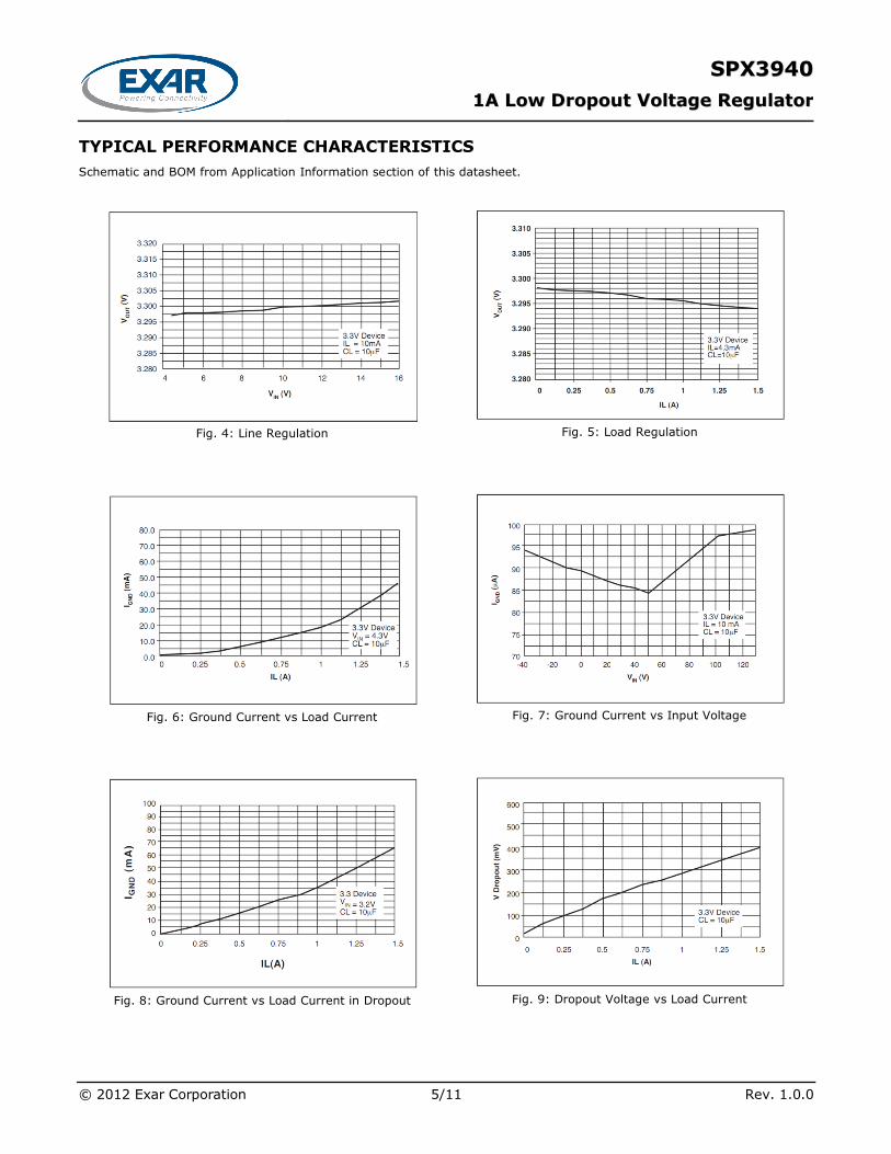
TYPICAL PERFORMANCE CHARACTERISTICS
Schematic and BOM from Application Information section of this datasheet.
Fig. 4: Line Regulation
Fig. 5: Load Regulation
Fig. 6: Ground Current vs Load Current
Fig. 7: Ground Current vs Input Voltage
Fig. 8: Ground Current vs Load Current in Dropout
Fig. 9: Dropout Voltage vs Load Current
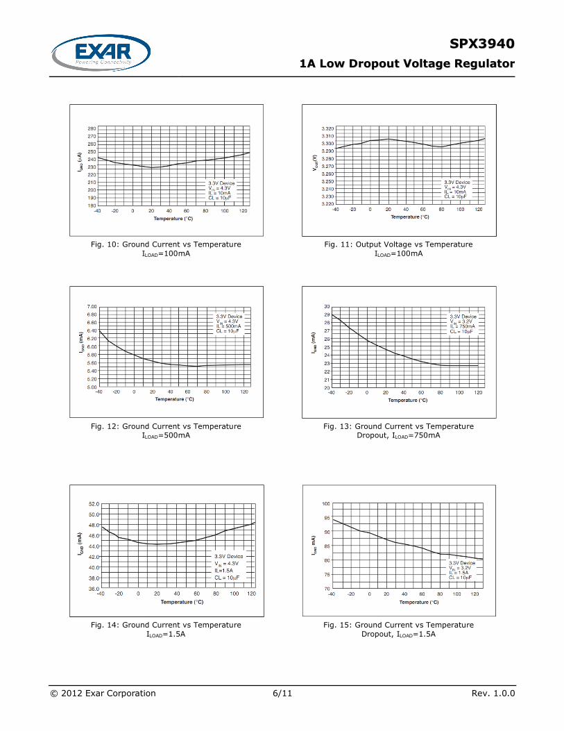
SSPPXX33994400
11AA LLooww DDrrooppoouutt VVoollttaaggee RReegguullaattoorr
© 2012 Exar Corporation 6/11 Rev. 1.0.0
Fig. 10: Ground Current vs Temperature
ILOAD=100mA
Fig. 11: Output Voltage vs Temperature
ILOAD=100mA
Fig. 12: Ground Current vs Temperature ILOAD=500mA
Fig. 13: Ground Current vs Temperature Dropout, ILOAD=750mA
Fig. 14: Ground Current vs Temperature
ILOAD=1.5A
Fig. 15: Ground Current vs Temperature
Dropout, ILOAD=1.5A
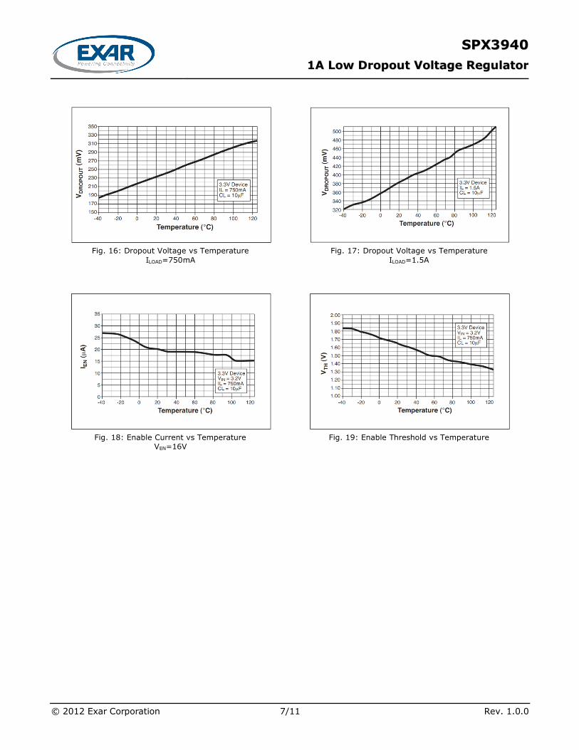
SSPPXX33994400
11AA LLooww DDrrooppoouutt VVoollttaaggee RReegguullaattoorr
© 2012 Exar Corporation 7/11 Rev. 1.0.0
Fig. 16: Dropout Voltage vs Temperature
ILOAD=750mA
Fig. 17: Dropout Voltage vs Temperature
ILOAD=1.5A
Fig. 18: Enable Current vs Temperature VEN=16V
Fig. 19: Enable Threshold vs Temperature
SSPPXX33994400
11AA LLooww DDrrooppoouutt VVoollttaaggee RReegguullaattoorr
© 2012 Exar Corporation 8/11 Rev. 1.0.0
THEORY OF OPERATION
The SPX3940 incorporates protection against over-current faults, reversed load insertion, over temperature operation, and positive and negative transient voltage.
THERMAL CONSIDERATIONS
Although the SPX3940 offers limiting circuitry
for overload conditions, it is still necessary to insure that the maximum junction temperature is not exceeded in the application. Heat will flow through the lowest resistance path, the junction-to-case path. In order to insure the best thermal flow of the component, proper mount-ing is required.
Consult heatsink manufacturer for thermal resistance and design of heatsink.
TO-220 Design Example:
Assume that VIN = 10V, VOUT = 5V, IOUT = 1.5A, TA = 50°C/W, θHA= 1°C/W, θCH = 2°C/W, and θJC = 3°C/W.
Where TA = ambient temperature
θHA = heatsink to ambient thermal resistance
θCH = case to heatsink thermal resistance
θJC = junction to case thermal resistance
The power calculated under these conditions is:
PD = (VIN – VOUT) * IOUT = 7.5W.
And the junction temperature is calculated as
TJ = TA + PD * (θHA + θCH + θJC) or
TJ = 50 + 7.5 * (1 + 2 + 3) = 95°C
Reliable operation is insured.
CAPACITOR REQUIREMENTS
The output capacitor is needed to insure stability and minimize the output noise. The value of the capacitor varies with the load.
However, a minimum value of 10µF aluminum capacitor will guarantee stability over all load conditions. A tantalum capacitor is recommended if a faster load transient response is needed.
If the power source has a high AC impedance, a 0.1µF ceramic capacitor between input & ground is recommended.
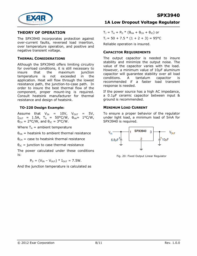
MINIMUM LOAD CURRENT
To ensure a proper behavior of the regulator under light load, a minimum load of 5mA for
SPX3940 is required.
Fig. 20: Fixed Output Linear Regulator
SSPPXX33994400
11AA LLooww DDrrooppoouutt VVoollttaaggee RReegguullaattoorr
© 2012 Exar Corporation 9/11 Rev. 1.0.0
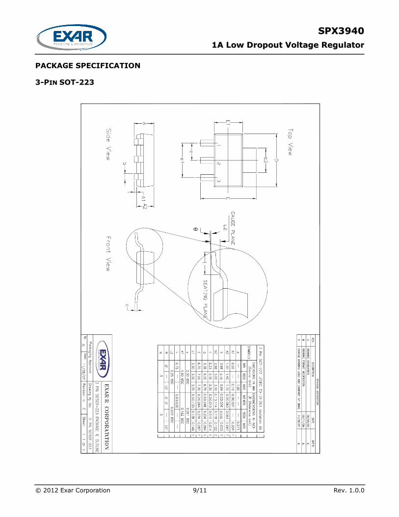
PACKAGE SPECIFICATION
3-PIN SOT-223
SSPPXX33994400
11AA LLooww DDrrooppoouutt VVoollttaaggee RReegguullaattoorr
© 2012 Exar Corporation 10/11 Rev. 1.0.0
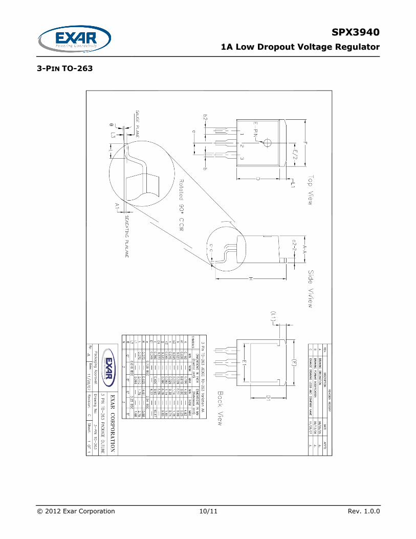
3-PIN TO-263
SSPPXX33994400
11AA LLooww DDrrooppoouutt VVoollttaaggee RReegguullaattoorr
© 2012 Exar Corporation 11/11 Rev. 1.0.0
REVISION HISTORY
Revision Date Description
A 04/14/2006
1.0.0 02/29/2012 Reformat of Datasheet
Package drawing corrections
FOR FURTHER ASSISTANCE
Email: [email protected]
Exar Technical Documentation: http://www.exar.com/TechDoc/default.aspx?
EXAR CORPORATION
HEADQUARTERS AND SALES OFFICES
48720 Kato Road
Fremont, CA 94538 – USA
Tel.: +1 (510) 668-7000
Fax: +1 (510) 668-7030
www.exar.com
NOTICE
EXAR Corporation reserves the right to make changes to the products contained in this publication in order to improve
design, performance or reliability. EXAR Corporation assumes no responsibility for the use of any circuits described herein, conveys no license under any patent or other right, and makes no representation that the circuits are free of patent
infringement. Charts and schedules contained here in are only for illustration purposes and may vary depending upon a user’s specific application. While the information in this publication has been carefully checked; no responsibility, however,
is assumed for inaccuracies.
EXAR Corporation does not recommend the use of any of its products in life support applications where the failure or
malfunction of the product can reasonably be expected to cause failure of the life support system or to significantly affect its safety or effectiveness. Products are not authorized for use in such applications unless EXAR Corporation receives, in
writing, assurances to its satisfaction that: (a) the risk of injury or damage has been minimized; (b) the user assumes all such risks; (c) potential liability of EXAR Corporation is adequately protected under the circumstances.
Reproduction, in part or whole, without the prior written consent of EXAR Corporation is prohibited.