Embed Size (px)
Citation preview
x Introduction to RISC and CISC: LECTURE 15
RISC (Reduced Instruction Set Computer)
RISC stands for Reduced Instruction Set Computer. To execute each instruction, if there is separate
electronic circuitry in the control unit, which produces all the necessary signals, this approach of the
design of the control section of the processor is called RISC design. It is also called hard-wired approach.
Examples of RISC processors:
x IBM RS6000, MC88100.
x DEC’s Alpha 21064, 21164 and 21264 processors
Features of RISC Processors: The standard features of RISC processors are listed below:
x RISC processors use a small and limited number of instructions.
x RISC machines mostly uses hardwired control unit.
x RISC processors consume less power and are having high performance.
x Each instruction is very simple and consistent.
x RISC processors uses simple addressing modes.
x RISC instruction is of uniform fixed length.
CISC (Complex Instruction Set Computer)
CISC stands for Complex Instruction Set Computer. If the control unit contains a number of micro-
electronic circuitry to generate a set of control signals and each micro-circuitry is activated by a micro-
code, this design approach is called CISC design.
Examples of CISC processors are:
x Intel 386, 486, Pentium, Pentium Pro, Pentium II, Pentium III
x Motorola’s 68000, 68020, 68040, etc.
Features of CISC Processors: The standard features of CISC processors are listed below:
x CISC chips have a large amount of different and complex instructions.
x CISC machines generally make use of complex addressing modes.
x Different machine programs can be executed on CISC machine.
x CISC machines uses micro-program control unit.
x CISC processors are having limited number of registers.
Ö DESIGNING A HYPOTHETICAL CPU: LECTURE 16
Processor Design
S1 simple CPU
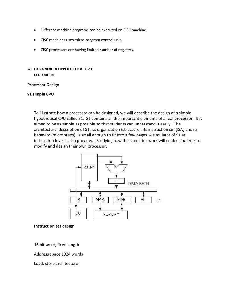
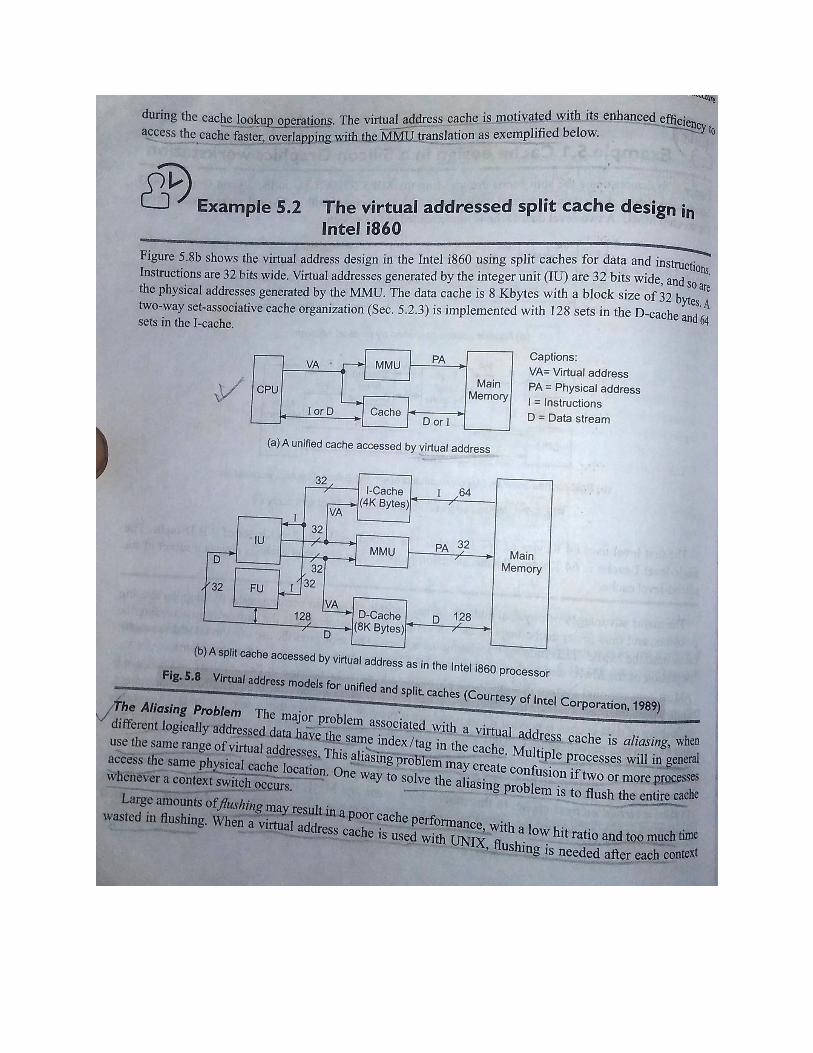
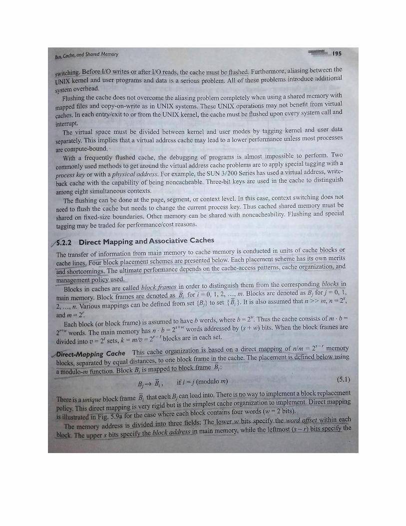
To illustrate how a processor can be designed, we will describe the design of a simple hypothetical CPU called S1. S1 contains all the important elements of a real processor. It is aimed to be as simple as possible so that students can understand it easily. The architectural description of S1: its organization (structure), its instruction set (ISA) and its behavior (micro steps), is small enough to fit into a few pages. A simulator of S1 at instruction level is also provided. Studying how the simulator work will enable students to modify and design their own processor.
Instruction set design
16 bit word, fixed length
Address space 1024 words
Load, store architecture
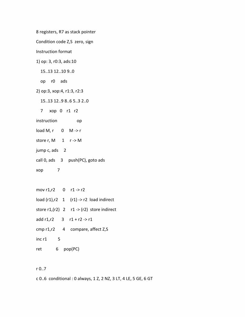
8 registers, R7 as stack pointer
Condition code Z,S zero, sign
Instruction format
1) op: 3, r0:3, ads:10
15..13 12..10 9..0
op r0 ads
2) op:3, xop:4, r1:3, r2:3
15..13 12..9 8..6 5..3 2..0
7 xop 0 r1 r2
instruction op
load M, r 0 M -> r
store r, M 1 r -> M
jump c, ads 2
call 0, ads 3 push(PC), goto ads
xop 7
mov r1,r2 0 r1 -> r2
load (r1),r2 1 (r1) -> r2 load indirect
store r1,(r2) 2 r1 -> (r2) store indirect
add r1,r2 3 r1 + r2 -> r1
cmp r1,r2 4 compare, affect Z,S
inc r1 5
ret 6 pop(PC)
r 0..7
c 0..6 conditional : 0 always, 1 Z, 2 NZ, 3 LT, 4 LE, 5 GE, 6 GT
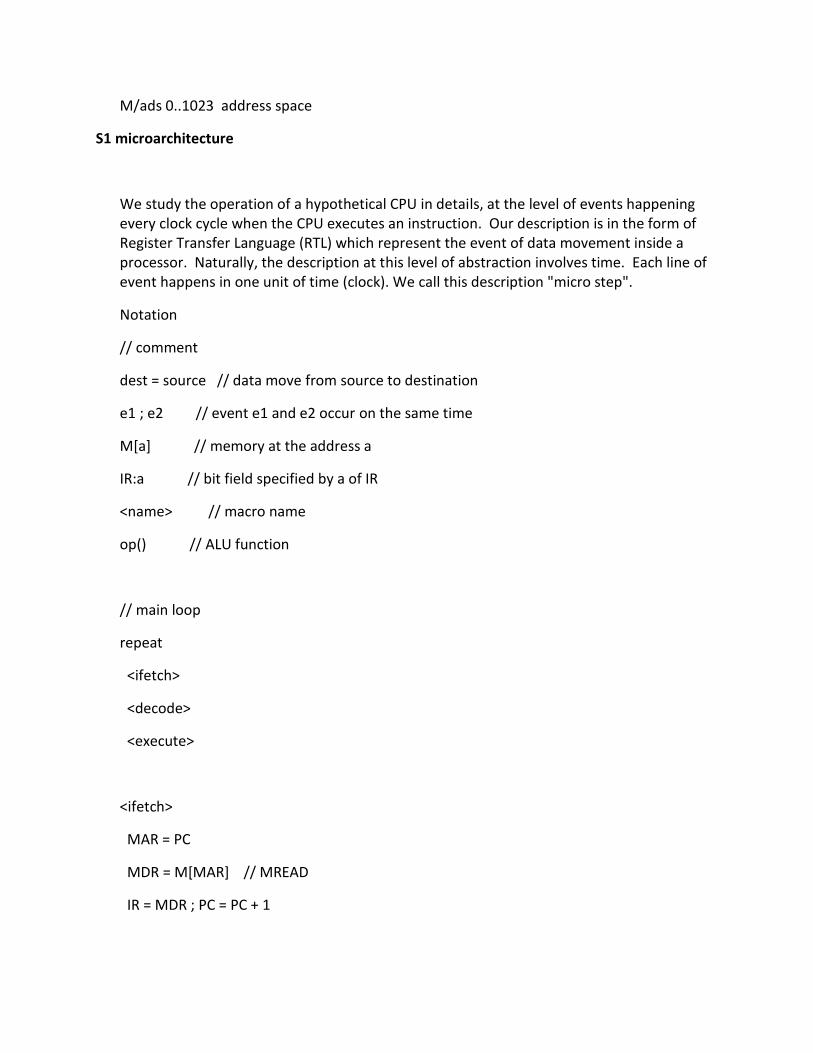
M/ads 0..1023 address space
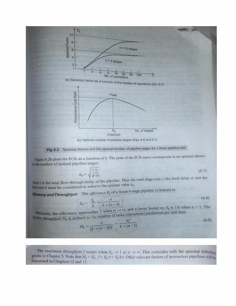
S1 microarchitecture
We study the operation of a hypothetical CPU in details, at the level of events happening every clock cycle when the CPU executes an instruction. Our description is in the form of Register Transfer Language (RTL) which represent the event of data movement inside a processor. Naturally, the description at this level of abstraction involves time. Each line of event happens in one unit of time (clock). We call this description "micro step".
Notation
// comment
dest = source // data move from source to destination
e1 ; e2 // event e1 and e2 occur on the same time
M[a] // memory at the address a
IR:a // bit field specified by a of IR
<name> // macro name
op() // ALU function
// main loop
repeat
<ifetch>
<decode>
<execute>
<ifetch>
MAR = PC
MDR = M[MAR] // MREAD
IR = MDR ; PC = PC + 1
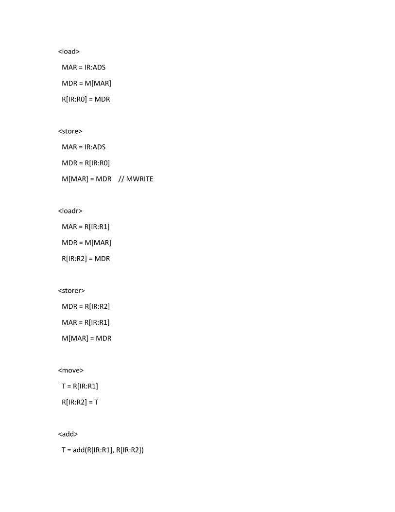
<load>
MAR = IR:ADS
MDR = M[MAR]
R[IR:R0] = MDR
<store>
MAR = IR:ADS
MDR = R[IR:R0]
M[MAR] = MDR // MWRITE
<loadr>
MAR = R[IR:R1]
MDR = M[MAR]
R[IR:R2] = MDR
<storer>
MDR = R[IR:R2]
MAR = R[IR:R1]
M[MAR] = MDR
<move>
T = R[IR:R1]
R[IR:R2] = T
<add>
T = add(R[IR:R1], R[IR:R2])
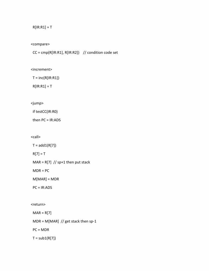
R[IR:R1] = T
<compare>
CC = cmp(R[IR:R1], R[IR:R2]) // condition code set
<increment>
T = inc(R[IR:R1])
R[IR:R1] = T
<jump>
if testCC(IR:R0)
then PC = IR:ADS
<call>
T = add1(R[7])
R[7] = T
MAR = R[7] // sp+1 then put stack
MDR = PC
M[MAR] = MDR
PC = IR:ADS
<return>
MAR = R[7]
MDR = M[MAR] // get stack then sp-1
PC = MDR
T = sub1(R[7])
R[7] = T
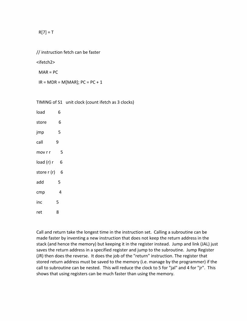
// instruction fetch can be faster
<ifetch2>
MAR = PC
IR = MDR = M[MAR]; PC = PC + 1
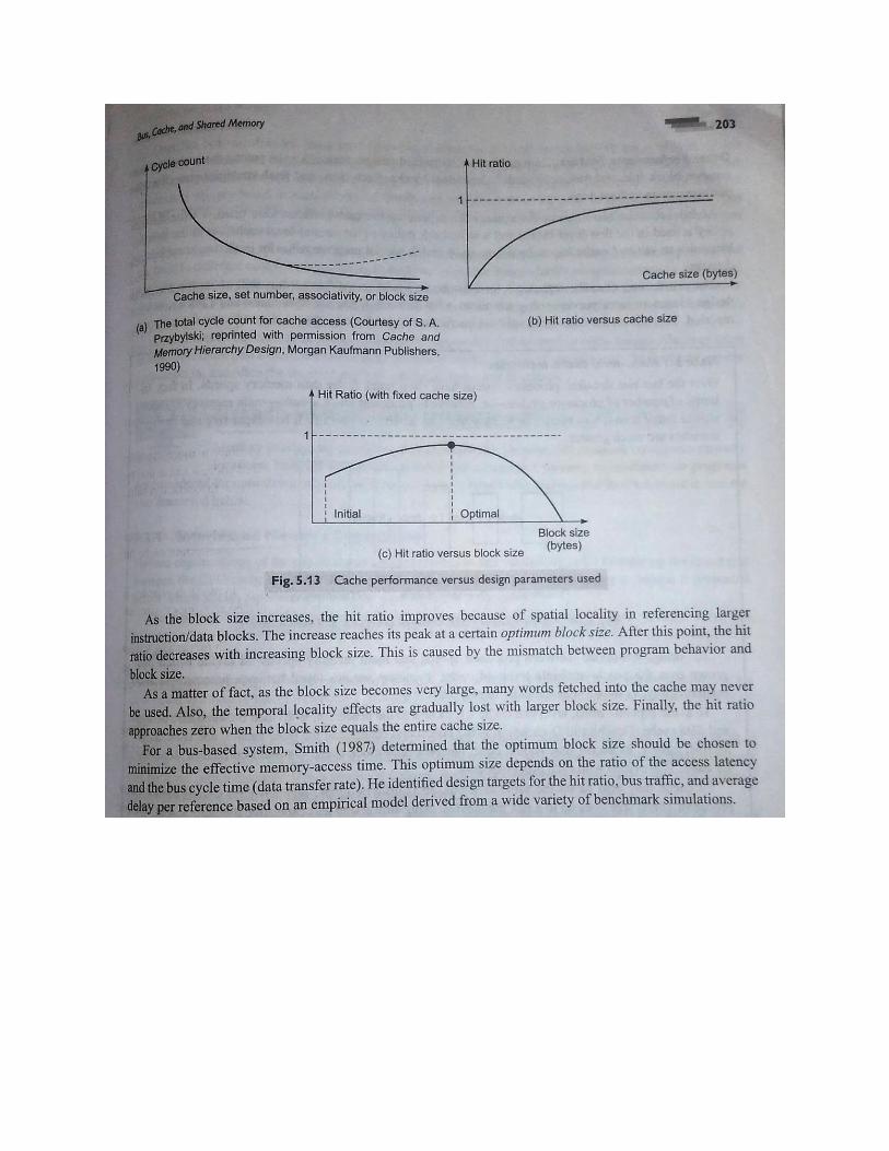
TIMING of S1 unit clock (count ifetch as 3 clocks)
load 6
store 6
jmp 5
call 9
mov r r 5
load (r) r 6
store r (r) 6
add 5
cmp 4
inc 5
ret 8
Call and return take the longest time in the instruction set. Calling a subroutine can be made faster by inventing a new instruction that does not keep the return address in the stack (and hence the memory) but keeping it in the register instead. Jump and link (JAL) just saves the return address in a specified register and jump to the subroutine. Jump Register (JR) then does the reverse. It does the job of the "return" instruction. The register that stored return address must be saved to the memory (i.e. manage by the programmer) if the call to subroutine can be nested. This will reduce the clock to 5 for "jal" and 4 for "jr". This shows that using registers can be much faster than using the memory.
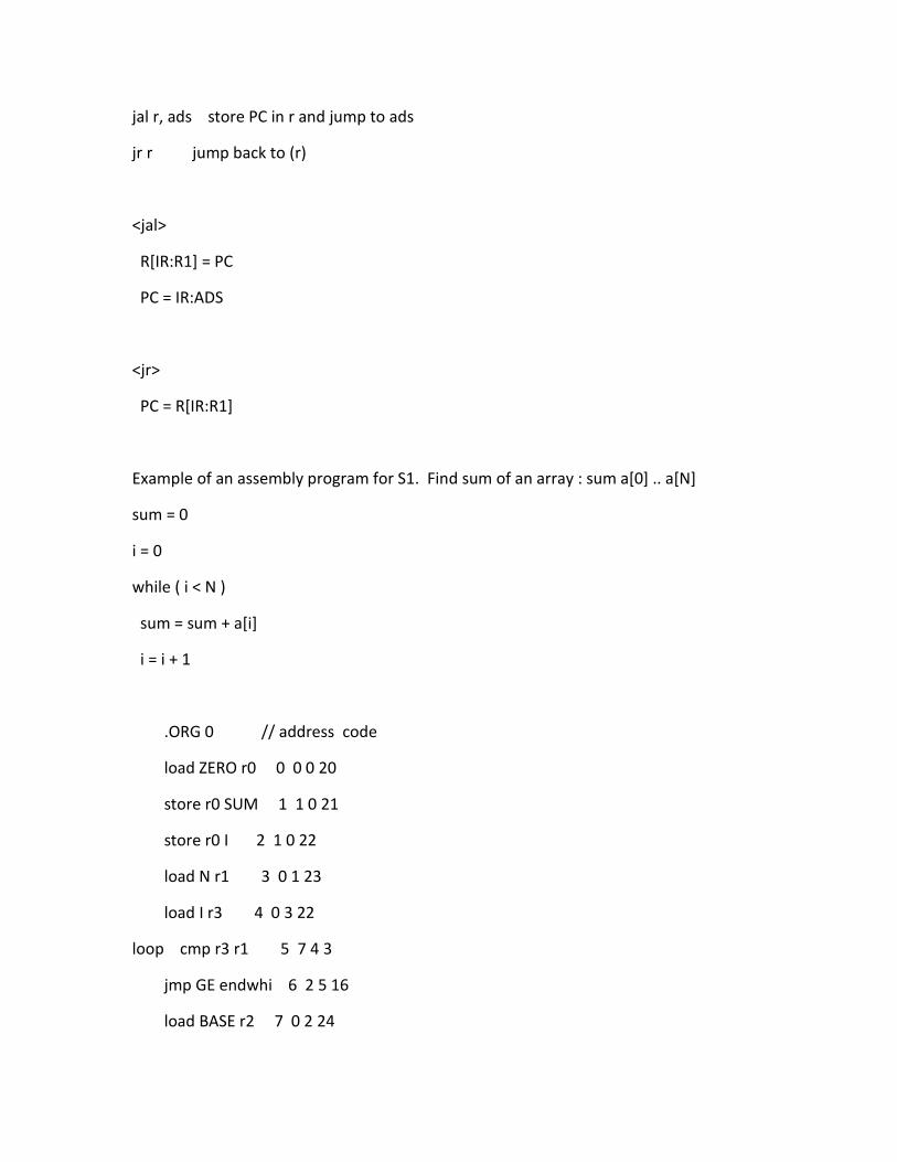
jal r, ads store PC in r and jump to ads
jr r jump back to (r)
<jal>
R[IR:R1] = PC
PC = IR:ADS
<jr>
PC = R[IR:R1]
Example of an assembly program for S1. Find sum of an array : sum a[0] .. a[N]
sum = 0
i = 0
while ( i < N )
sum = sum + a[i]
i = i + 1
.ORG 0 // address code
load ZERO r0 0 0 0 20
store r0 SUM 1 1 0 21
store r0 I 2 1 0 22
load N r1 3 0 1 23
load I r3 4 0 3 22
loop cmp r3 r1 5 7 4 3
jmp GE endwhi 6 2 5 16
load BASE r2 7 0 2 24
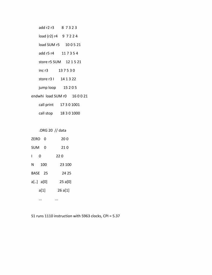
add r2 r3 8 7 3 2 3
load (r2) r4 9 7 2 2 4
load SUM r5 10 0 5 21
add r5 r4 11 7 3 5 4
store r5 SUM 12 1 5 21
inc r3 13 7 5 3 0
store r3 I 14 1 3 22
jump loop 15 2 0 5
endwhi load SUM r0 16 0 0 21
call print 17 3 0 1001
call stop 18 3 0 1000
.ORG 20 // data
ZERO 0 20 0
SUM 0 21 0
I 0 22 0
N 100 23 100
BASE 25 24 25
a[..] a[0] 25 a[0]
a[1] 26 a[1]
... ...
S1 runs 1110 instruction with 5963 clocks, CPI = 5.37
How to run the S1 simulator
The input file is an object file with the name "in.obj". When run s1 the simulator will start and load "in.obj" and execute starting from PC=0 until stop with the instruction call 1000
An object file has the following format
a ads set PC to ads
i op r ads instruction op
i 7 xop r1 r2 instruction xop
w data set that address to value "data"
t set trace mode on
d start nbyte dump memory n byte
e end of object file
x INSTRUCTION SET DESIGN: LECTURE 17
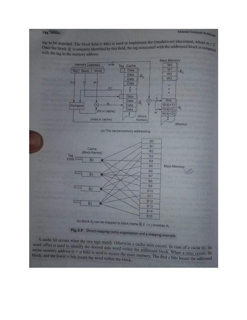
An instruction set is a collection of all instructions of a CPU. Therefore, if we define all the instructions of a computer, we can say we have defined the instruction set. Each instruction consists of several elements. An instruction element is a unit of information required by the CPU for execution.
Elements of an instruction: An instruction have the following elements.
x An operation code also termed as OP code which specifies the operation to be performed.
x A reference to the operands on which data processing is to be performed.
x A reference to the operands which may store results of data processing operation performed by the instruction.
x A reference for the next instruction to be fetched and executed.
The next instruction which is to be executed is normally the next instruction in the memory. Therefore, no explicit reference to the next instruction is provided.
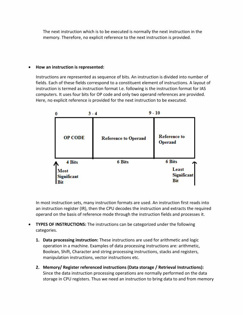
x How an instruction is represented:
Instructions are represented as sequence of bits. An instruction is divided into number of fields. Each of these fields correspond to a constituent element of instructions. A layout of instruction is termed as instruction format I.e. following is the instruction format for IAS computers. It uses four bits for OP code and only two operand references are provided. Here, no explicit reference is provided for the next instruction to be executed.
In most instruction sets, many instruction formats are used. An instruction first reads into an instruction register (IR), then the CPU decodes the instruction and extracts the required operand on the basis of reference mode through the instruction fields and processes it.
x TYPES OF INSTRUCTIONS: The instructions can be categorized under the following categories.
1. Data processing instruction: These instructions are used for arithmetic and logic operation in a machine. Examples of data processing instructions are: arithmetic, Boolean, Shift, Character and string processing instructions, stacks and registers, manipulation instructions, vector instructions etc.
2. Memory/ Register referenced instructions (Data storage / Retrieval Instructions): Since the data instruction processing operations are normally performed on the data storage in CPU registers. Thus we need an instruction to bring data to and from memory
to register. These are called data storage/ retrieval instructions. Example of data storage and retrieval instructions are load and store instructions.
3. Input output instructions (Data movement instruction): These are basically input output instructions. These are required to bring in programs and data from various devices to memory or to communicate results to the input output devices. Some of these instructions can be: start input / output, Halt input/ output, test input/ output, etc.
4. Control Instructions: These instructions are used for testing the status of computation through processor status word (PSW). Another of such instruction is the branch instruction used for transfer of control.
5. Miscellaneous Instructions: The instruction does not fit in any of the above categories. Some of these instructions are:
o Interrupts or supervisory call, swapping return from interruptions, halt instructions or some privileged instructions of operating system.
x ADDRESSING MODES OF SCHEMES: It is the way of specifying the operand part of instruction.
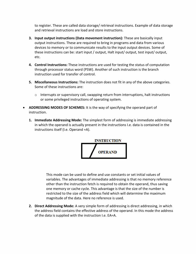
1. Immediate Addressing Mode: The simplest form of addressing is immediate addressing in which the operand is actually present in the instructions I.e. data is contained in the instructions itself (I.e. Operand =A).
This mode can be used to define and use constants or set initial values of variables. The advantages of immediate addressing is that no memory reference other than the instruction fetch is required to obtain the operand, thus saving one memory or cache cycle. This advantage is that the size of the number is restricted to the size of the address field which will determine the maximum magnitude of the data. Here no reference is used.
2. Direct Addressing Mode: A very simple form of addressing is direct addressing, in which the address field contains the effective address of the operand. In this mode the address of the data is supplied with the instruction I.e. EA=A.
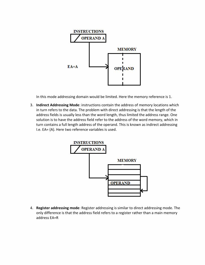
In this mode addressing domain would be limited. Here the memory reference is 1.
3. Indirect Addressing Mode: instructions contain the address of memory locations which in turn refers to the data. The problem with direct addressing is that the length of the address fields is usually less than the word length, thus limited the address range. One solution is to have the address field refer to the address of the word memory, which in turn contains a full length address of the operand. This is known as indirect addressing I.e. EA= (A). Here two reference variables is used.
4. Register addressing mode: Register addressing is similar to direct addressing mode. The only difference is that the address field refers to a register rather than a main memory address EA=R
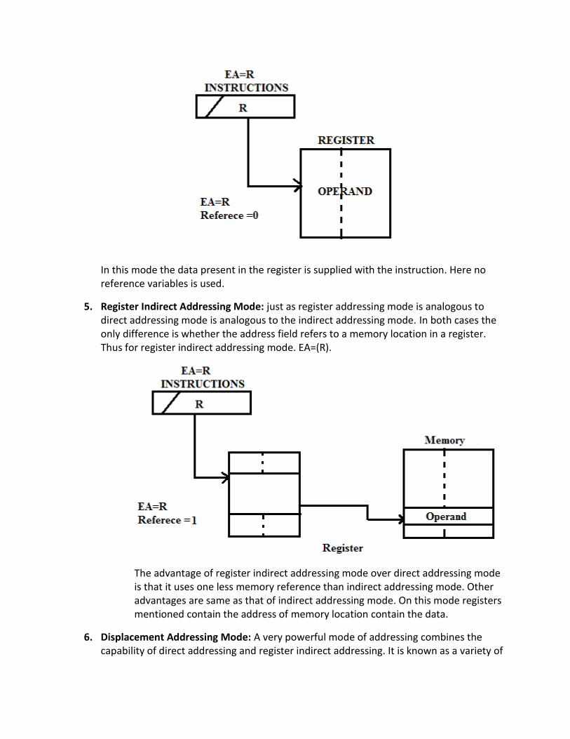
In this mode the data present in the register is supplied with the instruction. Here no reference variables is used.
5. Register Indirect Addressing Mode: just as register addressing mode is analogous to direct addressing mode is analogous to the indirect addressing mode. In both cases the only difference is whether the address field refers to a memory location in a register. Thus for register indirect addressing mode. EA=(R).
The advantage of register indirect addressing mode over direct addressing mode is that it uses one less memory reference than indirect addressing mode. Other advantages are same as that of indirect addressing mode. On this mode registers mentioned contain the address of memory location contain the data.
6. Displacement Addressing Mode: A very powerful mode of addressing combines the capability of direct addressing and register indirect addressing. It is known as a variety of
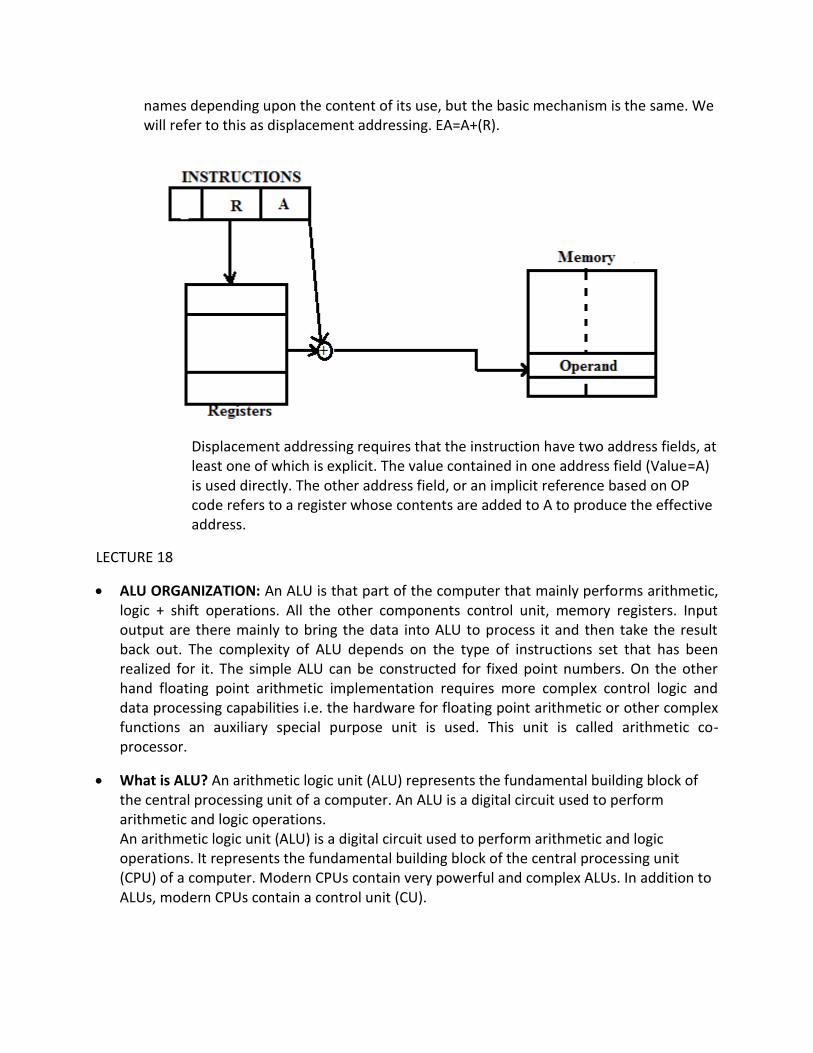
names depending upon the content of its use, but the basic mechanism is the same. We will refer to this as displacement addressing. EA=A+(R).
Displacement addressing requires that the instruction have two address fields, at least one of which is explicit. The value contained in one address field (Value=A) is used directly. The other address field, or an implicit reference based on OP code refers to a register whose contents are added to A to produce the effective address.
LECTURE 18
x ALU ORGANIZATION: An ALU is that part of the computer that mainly performs arithmetic, logic + shift operations. All the other components control unit, memory registers. Input output are there mainly to bring the data into ALU to process it and then take the result back out. The complexity of ALU depends on the type of instructions set that has been realized for it. The simple ALU can be constructed for fixed point numbers. On the other hand floating point arithmetic implementation requires more complex control logic and data processing capabilities i.e. the hardware for floating point arithmetic or other complex functions an auxiliary special purpose unit is used. This unit is called arithmetic co-processor.
x What is ALU? An arithmetic logic unit (ALU) represents the fundamental building block of the central processing unit of a computer. An ALU is a digital circuit used to perform arithmetic and logic operations. An arithmetic logic unit (ALU) is a digital circuit used to perform arithmetic and logic operations. It represents the fundamental building block of the central processing unit (CPU) of a computer. Modern CPUs contain very powerful and complex ALUs. In addition to ALUs, modern CPUs contain a control unit (CU).
Most of the operations of a CPU are performed by one or more ALUs, which load data from input registers. A register is a small amount of storage available as part of a CPU. The control unit tells the ALU what operation to perform on that data and the ALU stores the result in an output register. The control unit moves the data between these registers, the ALU, and memory.
CONTROL UNIT DESIGN: (LECTURE 19) the memory, arithmetic and logic unit input and output unit’s store and process information and perform input and output operations. The operation of these units must be coordinated in same way. This is the task of the control unit. The control unit is effectively the nerve center that sends control signals to other units and senses their states.
I/O transfers consisting of input and output operations and are controlled by the instructions of I/O programs that identify the devices involved and the information to be transferred. However the actual timing signal that lovers the transfer are generated by the control circuits. Timing signals are signals that determine when a given action is to take place. Data transfers between the processor and memory and are also controlled by the control unit through timing signals. It is reasonable to think of a control unit as a well-defined physical separate unit that interacts with other parts of the machine.
Much of the control circuitry is physically distributed through the machine. A large set of control line wires caries the signals used for timing and synchronization of events in all units. The operation of a computer can be summarized as follows:
o The computer accepts information in the form of programs and data through an input unit and stores in the memory.
o Information stored in the memory is fetched under program control into an arithmetic and logic unit, where it is processed.
o Processed information leaves the computer through an output unit.
o All activities inside the machine are directed by the control unit.
x STRUCTURE OF CONTROL UNIT: A control unit have set of input values on the basis of which it produces an output control signal which in turn performs micro-operation. The output signal control the execution of a program. A general model of a control unit is shown as:
The input of the control unit are as:
o The master clock signal: the signal causes micro-operation to be performed in a single clock cycle wither a single or a set of simultaneously micro-operation can be performed. The time taken in performing a single micro-operation is also termed as
processor cycle time in some machines. However, some micro-operation such as memory read may require more than one click cycle if it is greater than 1.
o The Instruction Register: the operation code (OP code) which normally include addressing mode bits of the instruction, help determining the various cycles to be performed an hence determines the related micro-operation which are needed to be performed.
o Flags: Flags are used by control unit for determining the status of the CPU. The outcomes of previous operation can also be detected using flags example as Y.A zero flag will help two control unit while executing an instruction, ISZ (skip the next instruction of zero flag is set). In case the zero flag is set the control unit will issue control signals which will cause program counter (PO) to be incremented by one.
o Control Signals from Control Bus: some of the control signals are provided to the control unit through the control bus. These signals are issued from outside the CPU some of these signals interrupt and acknowledge.
On the basis of input signals the control unit activities certain output control signals which in turn are responsible for the execution of an instruction. These output control signals are:
� Control signals which are required within CPU: these control signals causes two types of micro-operation viz for data transfer form one register to another and for performing an ALU operation using input and output registers.
� Control signals to control bus: the basis purpose of these control signals are to bring or to transfer data from CPU register to memory or I/O modules. The control signal are issued to the control bus to activate the data bus.
x Control Unit Organization: the basic responsibilities of the control unit is to control
� Data exchange of CPU with the memory or I/O modules.
� Internal operation in the CPU such as:
x Moving data between registers (register transfer operation).
x Making ALU to perform a particular operation on the data.
x Regulating other internal operation.
x Functional Requirements of a Control Unit: A control unit must know about the:
o Basic components of the CPU.
o Micro operation CPU performs, CPU of a computer consists of the following basic functional components.
� The arithmetic logic unit (ALU) which performs the basic arithmetic and logical operations.
� Registers which are used for information storage within the CPU.
� Internal data paths: these paths are useful for moving the data between two registers or between a register and ALU.
� External data paths: the role of these data paths are normally to link the CPu registers with the memory or I/O modules. This role is normally fulfilled by the system bus.
� The control unit which causes all the operations to happen in the CPU.
The micro-operations performed by the CPU can be classified as:
x Micro-operations for register to external interface I.e. (in most cases system bus data transfer).
x Micro-operations for external interface to register data transfer.
x Micro-operations for performing arithmetic and logic operations. These micro-operations involve use of registers for input and output.
The basic responsibilities of the control unit lies in the fact that the control unit must be able to guide the various components of CPU to perform a specific sequence of micro operation to achieve the execution of an instruction.
Thus, the control unit must perform two basic functions:
x Cause the execution of a micro-operation.
x Enable the CPU to execute a proper sequence of micro-operation which is determined by the instruction to be executed.
Ö Hardwired Control Unit: (LECTURE 20) A hardwired control unit is implemented as a logic circuits in the hardware. The inputs to control unit are: the instruction registers, flags, timing signals and control bus signals. On the basis of these inputs the output signal sequences are generated. Thus, output control signals are functions of inputs. Thus, we can derive a logical function for each control unit. The implementation of all the combinational circuits may be very difficult. Therefore a new approach microprogramming was used.
x Micro-programmed Control Unit: the hardwired control unit lack flexibility in design. In addition it is quite difficult to design, test and implement as in many computers the number of control lines is in hundreds.
Micro-program will consists of instruction, with each of the instruction describing.
o One or more micro-operations to be executed.
o The information about the micro-instruction to be executed next.
Such an instruction is termed as microinstruction and such a program is termed as a micro-program or firmware. The firmware is a midway between hardware and software. Firmware in comparison to hardware is easier to design, whereas in comparison to software is difficult to write. A control unit provides a set of control signal lines, distributed throughout the CPU, with each of the lines representing a zero or one. Therefore a microinstruction is made responsible for generating control signals for desired control lines to implement a desired micro-operation. Example: To implement a register to register transfer operation, output of the source register and input of destination register need to be enabled by the respective control signal line via a microinstruction. Thus, each microinstruction can generate a set of control signals on the control lines which in turn implement one or more micro-operation. A set of control signals with each bit representing a single control line is called a control word.
Thus, a microinstruction can cause execution of one or more micro-operations and a sequence of microinstructions that is micro-program, can cause execution of an instruction. The microprograms are mostly sored in read only memory, known as control store or control memory as alteration in control store are generally not required after the production of the control unit. In RAM such a memory instruction set of a computer can be changed by simple modifying the microprograms for various op-codes. Such a computer can be tailored for specific applications on the basis of microprograms. A computer having writable control memory are termed as “dynamically micro programmable” as the content of control memory for such computers can be changed under program control. The control memory is a word organized unit with each word representing a microinstruction. The computer which have micro programmed control unit have two separate memories: a main memory and the control memory.
Advantages of Micro Programmed Control Unit: since the microprograms can be changed relatively easily. Therefore micro-programmed control unit are very flexible in comparison to hardwired control unit.
Disadvantage:
x Hardware cost is more because of the control memory and its access circuitry.
x This is slower than hardwired control unit because the microinstruction are to be fetched from the control memory which is time consuming.
UNIT III
Ö The CPU Buses & I/O System:
Lecture 21 & 22
CPU BUS:
Definition 1: A collection of wires through which data is transmitted from one part of a
computer to another. You can think of a bus as a highway on which data travels within a
computer. When used in reference to personal computers, the term bus usually refers to
internal bus. This is a bus that connects all the internal computer components to the CPU and
main memory. There's also an expansion bus that enables expansion boards to access the CPU
and memory.
Definition 2: A CPU buses are a set of wires connecting various parts of the computer internally
and externally. They are used to send the data in the form of voltages. This data coluld be the
address of the memory location that needs to be accessed, or its contents or even the control
signals, indicating the type of operation to be performed on the memory. Based on the type of
information they are carrying, the buses are classified into three types.
1. Address Bus.
2. Data Bus.
3. Control Bus.
The bus could be used to send information from the CPU to one of the memory chips or some
I/O devices or vice versa or even in both the direction. I.e. from CPU to memory or I/O devices
and vice versa. The former are called unidirectional buses while the later are called as
bidirectional buses.
The size of a bus, known as its width, is important because it determines how much data can be
transmitted at one time. For example, a 16-bit bus can transmit 16 bits of data, whereas a 32-
bitbus can transmit 32 bits of data.
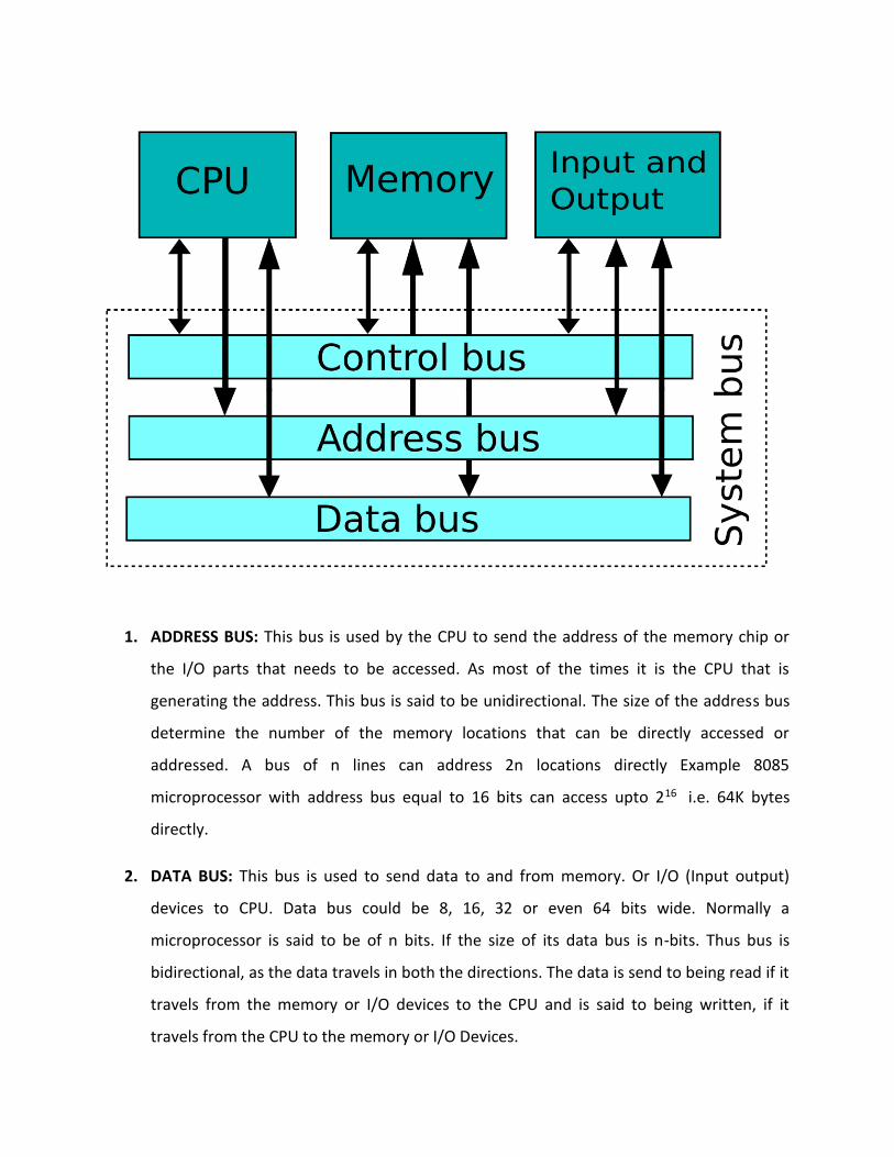
1. ADDRESS BUS: This bus is used by the CPU to send the address of the memory chip or
the I/O parts that needs to be accessed. As most of the times it is the CPU that is
generating the address. This bus is said to be unidirectional. The size of the address bus
determine the number of the memory locations that can be directly accessed or
addressed. A bus of n lines can address 2n locations directly Example 8085
microprocessor with address bus equal to 16 bits can access upto 216 i.e. 64K bytes
directly.
2. DATA BUS: This bus is used to send data to and from memory. Or I/O (Input output)
devices to CPU. Data bus could be 8, 16, 32 or even 64 bits wide. Normally a
microprocessor is said to be of n bits. If the size of its data bus is n-bits. Thus bus is
bidirectional, as the data travels in both the directions. The data is send to being read if it
travels from the memory or I/O devices to the CPU and is said to being written, if it
travels from the CPU to the memory or I/O Devices.
3. CONTROL BUS: Control bus contains various control signals that are used to control
various devices connected to the CPU. The control signal vary from the microprocessor to
the microprocessor.
Lecture 23 BUS ARBITER: The device that is allowed to initiate data transfers on the bus at any
given time is called the bus master. In a computer system there may be more than one bus
master such as processor, DMA controller etc.
They share the system bus. When current master relinquishes control of the bus, another bus
master can acquire the control of the bus.
Bus arbitration is the process by which the next device to become the bus master is selected and
bus mastership is transferred to it. The selection of bus master is usually done on the priority
basis.
There are two approaches to bus arbitration:
1. Centralized.
2. Distributed.
1. Centralized Arbitration: In centralized bus arbitration, a single bus arbiter performs the
required arbitration. The bus arbiter may be the processor or a separate controller connected to
the bus.
There are three different arbitration schemes that use the centralized bus arbitration approach.
There schemes are:
a. Daisy chaining.
b. Polling method.
c. Independent request.
A. Daisy Chaining: The system connections for Daisy chaining method are shown in fig below.
Enter image description here
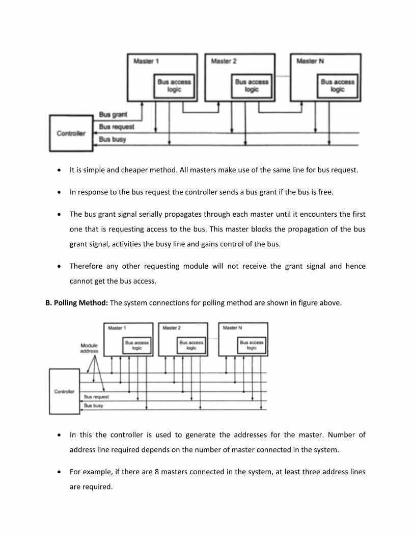
x It is simple and cheaper method. All masters make use of the same line for bus request.
x In response to the bus request the controller sends a bus grant if the bus is free.
x The bus grant signal serially propagates through each master until it encounters the first
one that is requesting access to the bus. This master blocks the propagation of the bus
grant signal, activities the busy line and gains control of the bus.
x Therefore any other requesting module will not receive the grant signal and hence
cannot get the bus access.
B. Polling Method: The system connections for polling method are shown in figure above.
x In this the controller is used to generate the addresses for the master. Number of
address line required depends on the number of master connected in the system.
x For example, if there are 8 masters connected in the system, at least three address lines
are required.
x In response to the bus request controller generates a sequence of master address. When
the requesting master recognizes its address, it activated the busy line ad begins to use
the bus.
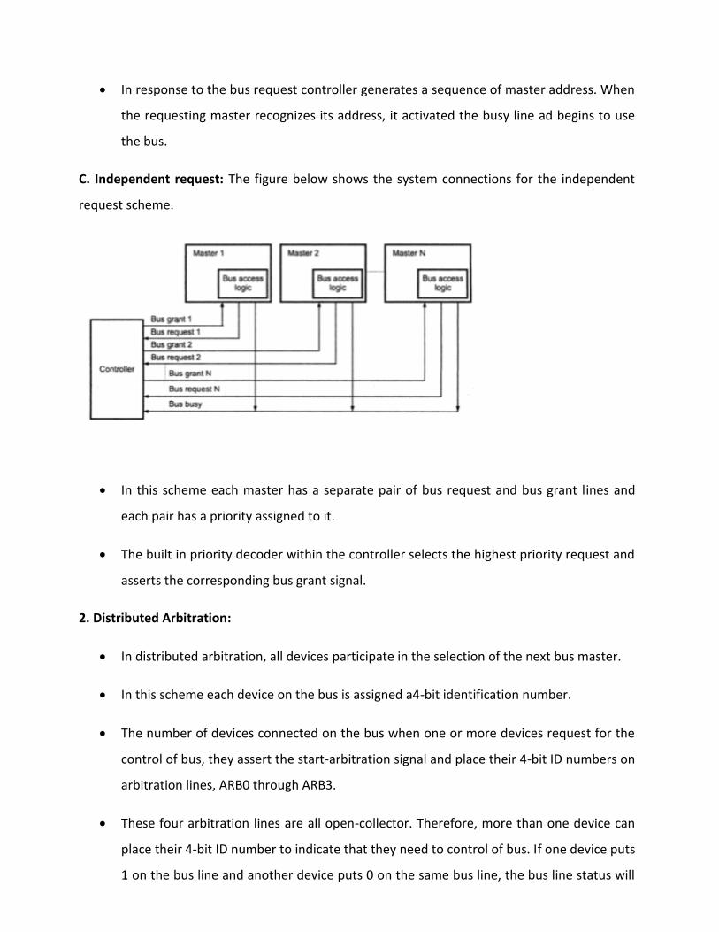
C. Independent request: The figure below shows the system connections for the independent
request scheme.
x In this scheme each master has a separate pair of bus request and bus grant lines and
each pair has a priority assigned to it.
x The built in priority decoder within the controller selects the highest priority request and
asserts the corresponding bus grant signal.
2. Distributed Arbitration:
x In distributed arbitration, all devices participate in the selection of the next bus master.
x In this scheme each device on the bus is assigned a4-bit identification number.
x The number of devices connected on the bus when one or more devices request for the
control of bus, they assert the start-arbitration signal and place their 4-bit ID numbers on
arbitration lines, ARB0 through ARB3.
x These four arbitration lines are all open-collector. Therefore, more than one device can
place their 4-bit ID number to indicate that they need to control of bus. If one device puts
1 on the bus line and another device puts 0 on the same bus line, the bus line status will
be 0. Device reads the status of all lines through inverters buffers so device reads bus
status 0as logic 1. Scheme the device having highest ID number has highest priority.
x When two or more devices place their ID number on bus lines then it is necessary to
identify the highest ID number on bus lines then it is necessary to identify the highest ID
number from the status of bus line. Consider that two devices A and B, having ID number
1 and 6, respectively are requesting the use of the bus.
x Device A puts the bit pattern 0001, and device B puts the bit pattern 0110. With this
combination the status of bus-line will be 1000; however because of inverter buffers
code seen by both devices is 0111.
x Each device compares the code formed on the arbitration line to its own ID, starting from
the most significant bit. If it finds the difference at any bit position, it disables its drives at
that bit position and for all lower-order bits.
x It does so by placing a 0 at the input of their drive. In our example, device detects a
different on line ARB2 and hence it disables its drives on line ARB2, ARB1 and ARB0. This
causes the code on the arbitration lines to change to 0110. This means that device B has
won the race.
x The decentralized arbitration offers high reliability because operation of the bus is not
dependent on any single device.
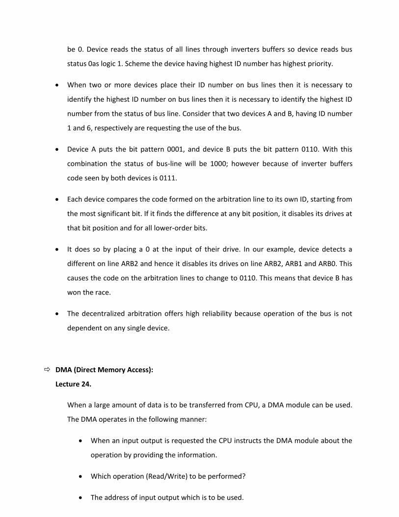
Ö DMA (Direct Memory Access):
Lecture 24.
When a large amount of data is to be transferred from CPU, a DMA module can be used.
The DMA operates in the following manner:
x When an input output is requested the CPU instructs the DMA module about the
operation by providing the information.
x Which operation (Read/Write) to be performed?
x The address of input output which is to be used.
x The starting location on the memory where the information will be read and
written.
x The number of words to be read or written again, communicated via the data
lines and stored in the data counter register.
The DMA module transfers the request block byte by byte directly to the memory
without interleaving the CPU. On completion of the request, DMA module sends an interrupt
signal to the CPU. This is DMA the CPU involvement can be restricted at beginning and at the
end of the transfer, in the meantime CPU execute another program or may be another part of
the same program.
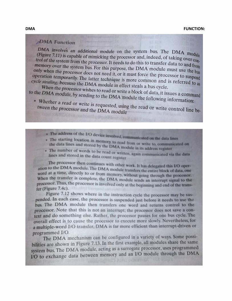
DMA FUNCTION:
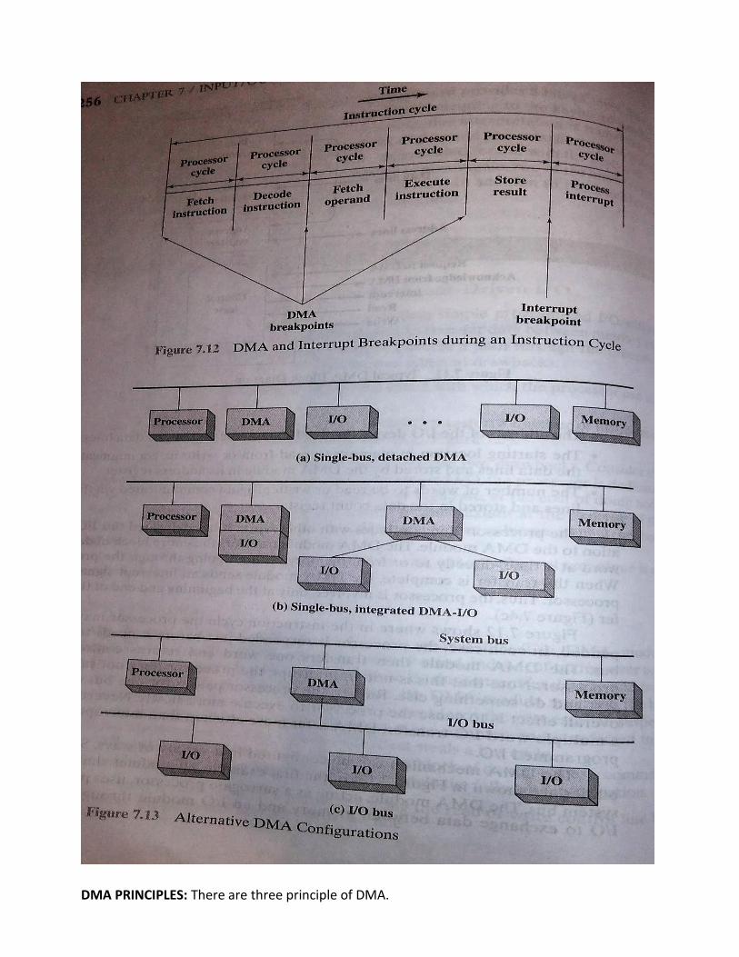
DMA PRINCIPLES: There are three principle of DMA.
1. Third Party DMA.
2. Bus Mastering.
3. Transfer Types.
1. Third Party DMA: Standard DMA, also called third-party DMA, uses a DMA controller. A
DMA controller can generate memory addresses and initiate memory read or write
cycles. It contains several hardware registers that can be written and read by the CPU.
These include a memory address register, a byte count register, and one or more control
registers. The control registers specify the I/O port to use, the direction of the transfer
(reading from the I/O device or writing to the I/O device), the transfer unit (byte at a time
or word at a time), and the number of bytes to transfer in one burst.
To carry out an input, output or memory-to-memory operation, the host processor
initializes the DMA controller with a count of the number of words to transfer, and the
memory address to use. The CPU then sends commands to a peripheral device to initiate
transfer of data. The DMA controller then provides addresses and read/write control
lines to the system memory. Each time a byte of data is ready to be transferred between
the peripheral device and memory, the DMA controller increments its internal address
register until the full block of data is transferred.
2. Bus Mastering: In a bus mastering system, also known as a first-party DMA system, the
CPU and peripherals can each be granted control of the memory bus. Where a peripheral
can become bus master, it can directly write to system memory without involvement of
the CPU, providing memory address and control signals as required. Some measure must
be provided to put the processor into a hold condition so that bus contention does not
occur.
3. Transfer Types: DMA transfers can either occur one byte at a time or all at once in burst
mode. If they occur a byte at a time, this can allow the CPU to access memory on
alternate bus cycles – this is called cycle stealing since the CPU and either the DMA
controller or the bus master contend for memory access. In burst mode DMA, the CPU
can be put on hold while the DMA transfer occurs and a full block of possibly hundreds or
thousands of bytes can be moved. When memory cycles are much faster than processor
cycles, an interleaved DMA cycle is possible, where the DMA controller uses memory
while the CPU cannot.
MODES OF OPERATION: There are three modes of operation.
1. Burst Mode: An entire block of data is transferred in one contiguous sequence. Once the
DMA controller is granted access to the system bus by the CPU, it transfers all bytes of
data in the data block before releasing control of the system buses back to the CPU, but
renders the CPU inactive for relatively long periods of time. The mode is also called
"Block Transfer Mode". It is also used to stop unnecessary data.
2. Cycle Stealing Mode: The cycle stealing mode is used in systems in which the CPU should
not be disabled for the length of time needed for burst transfer modes. In the cycle
stealing mode, the DMA controller obtains access to the system bus the same way as in
burst mode, using BR (Bus Request) and BG (Bus Grant) signals, which are the two signals
controlling the interface between the CPU and the DMA controller. However, in cycle
stealing mode, after one byte of data transfer, the control of the system bus is
deasserted to the CPU via BG. It is then continually requested again via BR, transferring
one byte of data per request, until the entire block of data has been transferred. By
continually obtaining and releasing the control of the system bus, the DMA controller
essentially interleaves instruction and data transfers. The CPU processes an instruction,
then the DMA controller transfers one data value, and so on. On the one hand, the data
block is not transferred as quickly in cycle stealing mode as in burst mode, but on the
other hand the CPU is not idled for as long as in burst mode. Cycle stealing mode is useful
for controllers that monitor data in real time.
3. Transparent Mode: Transparent mode takes the most time to transfer a block of data,
yet it is also the most efficient mode in terms of overall system performance. In
transparent mode, the DMA controller transfers data only when the CPU is performing
operations that do not use the system buses. The primary advantage of transparent
mode is that the CPU never stops executing its programs and the DMA transfer is free in
terms of time, while the disadvantage is that the hardware needs to determine when the
CPU is not using the system buses, which can be complex.
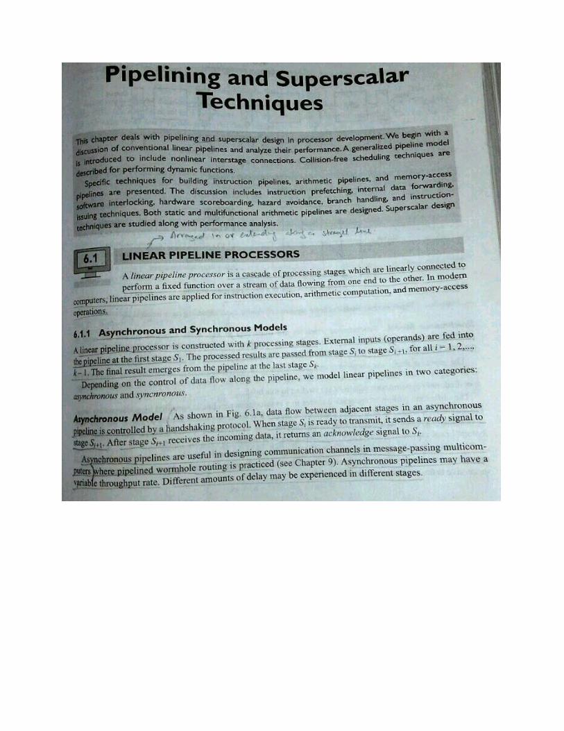
Ö WHAT IS PIPELINING?
Lecture 25 and 26
In computers, a pipeline is the continuous and somewhat overlapped movement of
instruction to the processor or in the arithmetic steps taken by the processor to perform
an instruction. Pipelining is the use of a pipeline. Without a pipeline, a computer
processor gets the first instruction from memory, performs the operation it calls for, and
then goes to get the next instruction from memory, and so forth. While fetching (getting)
the instruction, the arithmetic part of the processor is idle. It must wait until it gets the
next instruction. With pipelining, the computer architecture allows the next instructions
to be fetched while the processor is performing arithmetic operations, holding them in a
buffer close to the processor until each instruction operation can be performed. The
staging of instruction fetching is continuous. The result is an increase in the number of
instructions that can be performed during a given time period.
Pipelining is sometimes compared to a manufacturing assembly line in which different
parts of a product are being assembled at the same time although ultimately there may
be some parts that have to be assembled before others are. Even if there is some
sequential dependency, the overall process can take advantage of those operations that
can proceed concurrently.
Computer processor pipelining is sometimes divided into an instruction pipeline and an
arithmetic pipeline. The instruction pipeline represents the stages in which an instruction
is moved through the processor, including its being fetched, perhaps buffered, and then
executed. The arithmetic pipeline represents the parts of an arithmetic operation that
can be broken down and overlapped as they are performed.
Pipelines and pipelining also apply to computer memory controllers and moving data
through various memory staging places.
Ö BASIC CONCEPTS OF PIPELINING, THROUGHPUT AND SPEEDUP OF DATAPATHS:
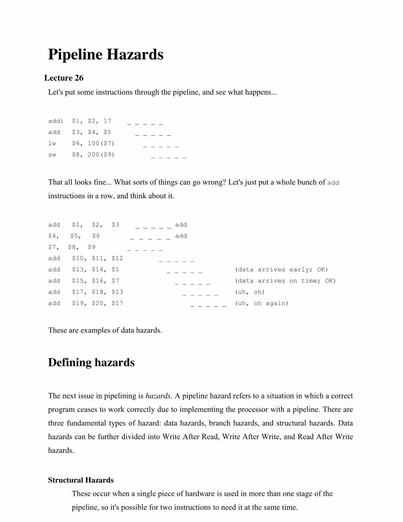
Pipeline Hazards Lecture 26 Let's put some instructions through the pipeline, and see what happens...
addi $1, $2, 17 _ _ _ _ _ add $3, $4, $5 _ _ _ _ _ lw $6, 100($7) _ _ _ _ _ sw $8, 200($9) _ _ _ _ _
That all looks fine... What sorts of things can go wrong? Let's just put a whole bunch of add
instructions in a row, and think about it.
add $1, $2, $3 _ _ _ _ _ add $4, $5, $6 _ _ _ _ _ add $7, $8, $9 _ _ _ _ _ add $10, $11, $12 _ _ _ _ _ add $13, $14, $1 _ _ _ _ _ (data arrives early; OK) add $15, $16, $7 _ _ _ _ _ (data arrives on time; OK) add $17, $18, $13 _ _ _ _ _ (uh, oh) add $19, $20, $17 _ _ _ _ _ (uh, oh again)
These are examples of data hazards.
Defining hazards
The next issue in pipelining is hazards. A pipeline hazard refers to a situation in which a correct
program ceases to work correctly due to implementing the processor with a pipeline. There are
three fundamental types of hazard: data hazards, branch hazards, and structural hazards. Data
hazards can be further divided into Write After Read, Write After Write, and Read After Write
hazards.
Structural Hazards
These occur when a single piece of hardware is used in more than one stage of the
pipeline, so it's possible for two instructions to need it at the same time.
So, for instance, suppose we'd only used a single memory unit instead of separate
instruction memory and data memories. A simple (non-pipelined) implementation would
work equally well with either approach, but in a pipelined implementation we'd run into
trouble any time we wanted to fetch an instruction at the same time a lw or sw was
reading or writing its data.
In effect, the pipeline design we're starting from has anticipated and resolved this hazard
by adding extra hardware.
Interestingly, the earlier editions of our text used a simple implementation with only a
single memory, and separated it into an instruction memory and a data memory when
they introduced pipelining. This edition starts right off with the two memories.
Also, the first Sparc implementations (remember, Sparc is almost exactly the RISC
machine defined by one of the authors) did have exactly this hazard, with the result that
load instructions took an extra cycle and store instructions took two extra cycles.
Data Hazards
This is when reads and writes of data occur in a different order in the pipeline than in the
program code. There are three different types of data hazard (named according to the
order of operations that must be maintained):
RAW
A Read After Write hazard occurs when, in the code as written, one instruction reads a
location after an earlier instruction writes new data to it, but in the pipeline the write
occurs after the read (so the instruction doing the read gets stale data).
WAR
A Write After Read hazard is the reverse of a RAW: in the code a write occurs after a
read, but the pipeline causes write to happen first.
WAW
A Write After Write hazard is a situation in which two writes occur out of order. We
normally only consider it a WAW hazard when there is no read in between; if there is,
then we have a RAW and/or WAR hazard to resolve, and by the time we've gotten that
straightened out the WAW has likely taken care of itself.
(the text defines data hazards, but doesn't mention the further subdivision into RAW,
WAR, and WAW. Their graduate level text mentions those)
Control Hazards
This is when a decision needs to be made, but the information needed to make the
decision is not available yet. A Control Hazard is actually the same thing as a RAW data
hazard (see above), but is considered separately because different techniques can be
employed to resolve it - in effect, we'll make it less important by trying to make good
guesses as to what the decision is going to be.
Two notes: First, there is no such thing as a RAR hazard, since it doesn't matter if reads occur
out of order. Second, in the MIPS pipeline, the only hazards possible are branch hazards and
RAW data hazards.
Resolving Hazards
There are four possible techniques for resolving a hazard. In order of preference, they are:
1. Forward. If the data is available somewhere, but is just not where we want it, we can
create extra data paths to ``forward'' the data to where it is needed. This is the best
solution, since it doesn't slow the machine down and doesn't change the semantics of the
instruction set. All of the hazards in the example above can be handled by forwarding.
2. Add hardware. This is most appropriate to structural hazards; if a piece of hardware has
to be used twice in an instruction, see if there is a way to duplicate the hardware. This is
exactly what the example MIPS pipeline does with the two memory units (if there were
only one, as was the case with RISC and early SPARC, instruction fetches would have to stall
waiting for memory reads and writes), and the use of an ALU and two dedicated adders.
3. Stall. We can simply make the later instruction wait until the hazard resolves itself.
This is undesireable because it slows down the machine, but may be necessary.
Handling a hazard on waiting for data from memory by stalling would be an example
here. Notice that the hazard is guaranteed to resolve itself eventually, since it wouldn't
have existed if the machine hadn't been pipelined. By the time the entire downstream
pipe is empty the effect is the same as if the machine hadn't been pipelined, so the
hazard has to be gone by then.
4. Document (AKA punt). Define instruction sequences that are forbidden, or change the
semantics of instructions, to account for the hazard. Examples are delayed loads and
delayed branches. This is the worst solution, both because it results in obscure
conditions on permissible instruction sequences, and (more importantly) because it ties
the instruction set to a particular pipeline implementation. A later implementation is
likely to have to use forwarding or stalls anyway, while emulating the hazards that
existed in the earlier implementation. Both Sparc and MIPS have been bitten by this;
one of the nice things about the late, lamented Alpha was the effort they put into
creating an exceptionally "clean" sequential semantics for the instruction set, to avoid
backward compatibility issues tying them to old implementations.
Hazards and Pipeline Diagrams
The definitions I put up above are all very nice, but they're a bit abstract. We can actually get
a pretty good picture of what's going on regarding hazards by inspecting the pipeline
diagram. First, remember the interpretation of the diagram:
1. Every row of the diagram is an instruction
2. Every column of the diagram is a time unit
3. Every "tick" in the diagram is a piece of hardware
This gives us some rules for the diagram:
• Data can only move horizontally (down the pipeline) or vertically (forwarding). It can't
go on a diagonal: if you're trying to move it forward in time (to the right), you have to
move it horizontally down the pipeline until the right time to forward it, then it has to
move vertically to the unit that needs it. It simply can't go back in time at all (if it
could, I could watch tomorrow's horse races and retire in very short order!).
• One piece of hardware can only be used by one instruction at a time.
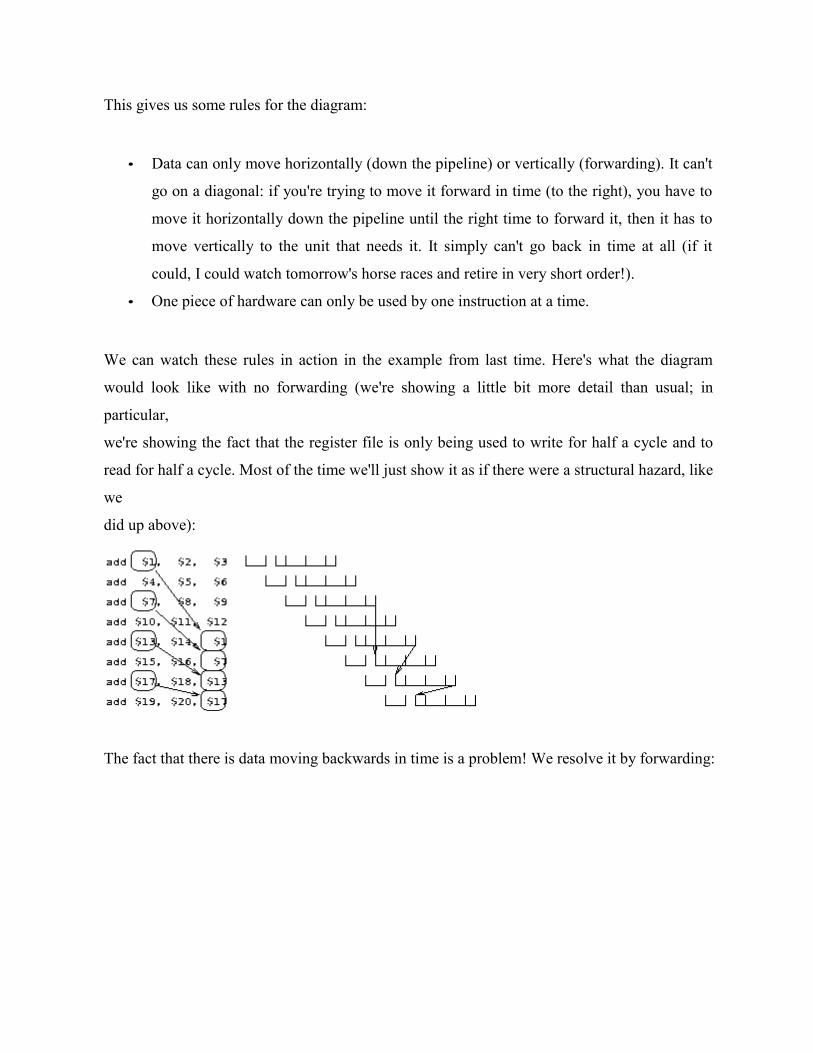
We can watch these rules in action in the example from last time. Here's what the diagram
would look like with no forwarding (we're showing a little bit more detail than usual; in
particular,
we're showing the fact that the register file is only being used to write for half a cycle and to
read for half a cycle. Most of the time we'll just show it as if there were a structural hazard, like
we
did up above):
The fact that there is data moving backwards in time is a problem! We resolve it by forwarding:
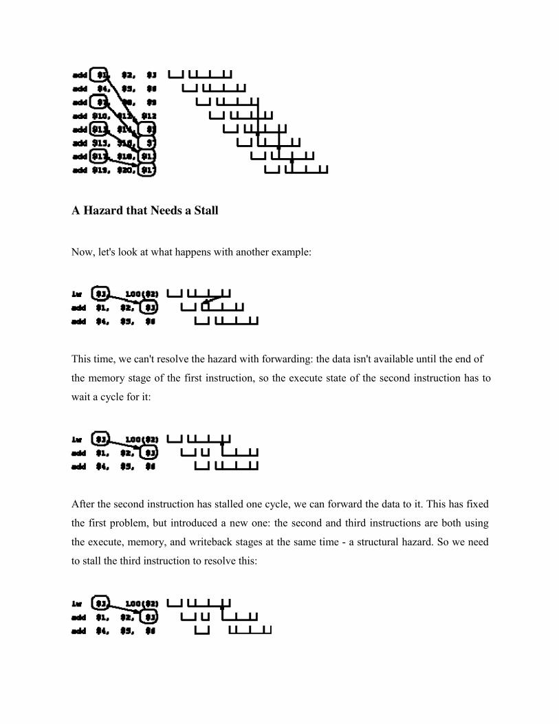
A Hazard that Needs a Stall
Now, let's look at what happens with another example:
This time, we can't resolve the hazard with forwarding: the data isn't available until the end of
the memory stage of the first instruction, so the execute state of the second instruction has to
wait a cycle for it:
After the second instruction has stalled one cycle, we can forward the data to it. This has fixed
the first problem, but introduced a new one: the second and third instructions are both using
the execute, memory, and writeback stages at the same time - a structural hazard. So we need
to stall the third instruction to resolve this:
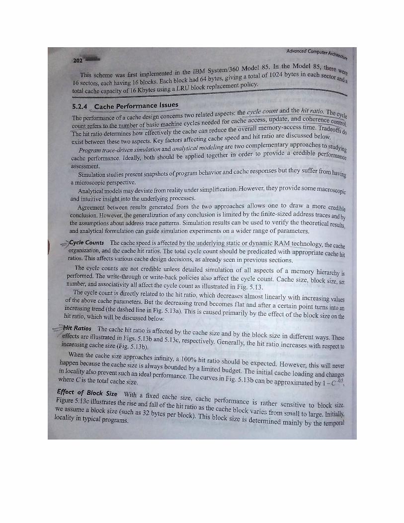
Ö MEMORY HIERARCHY:
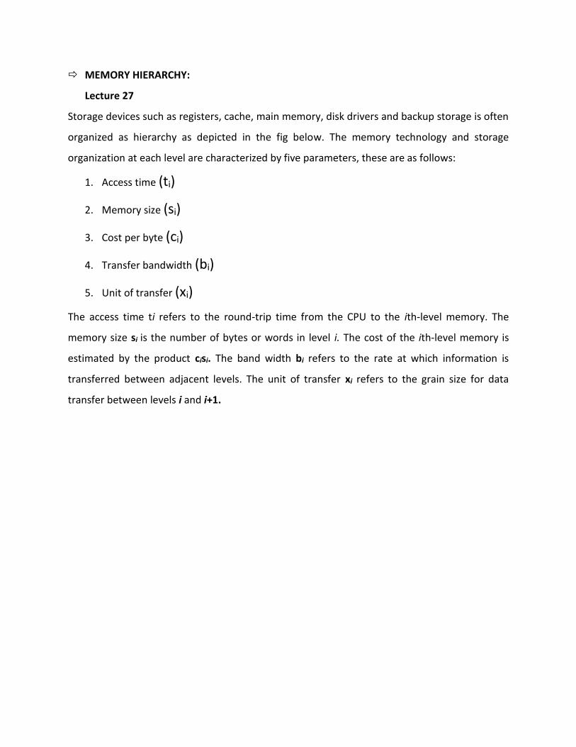
Lecture 27
Storage devices such as registers, cache, main memory, disk drivers and backup storage is often
organized as hierarchy as depicted in the fig below. The memory technology and storage
organization at each level are characterized by five parameters, these are as follows:
1. Access time (ti)
2. Memory size (si)
3. Cost per byte (ci)
4. Transfer bandwidth (bi)
5. Unit of transfer (xi)
The access time ti refers to the round-trip time from the CPU to the ith-level memory. The
memory size si is the number of bytes or words in level i. The cost of the ith-level memory is
estimated by the product cisi. The band width bi refers to the rate at which information is
transferred between adjacent levels. The unit of transfer xi refers to the grain size for data
transfer between levels i and i+1.
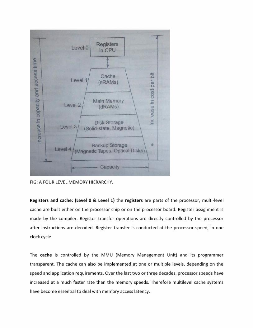
FIG: A FOUR LEVEL MEMORY HIERARCHY.
Registers and cache: (Level 0 & Level 1) the registers are parts of the processor, multi-level
cache are built either on the processor chip or on the processor board. Register assignment is
made by the compiler. Register transfer operations are directly controlled by the processor
after instructions are decoded. Register transfer is conducted at the processor speed, in one
clock cycle.
The cache is controlled by the MMU (Memory Management Unit) and its programmer
transparent. The cache can also be implemented at one or multiple levels, depending on the
speed and application requirements. Over the last two or three decades, processor speeds have
increased at a much faster rate than the memory speeds. Therefore multilevel cache systems
have become essential to deal with memory access latency.
Main Memory (Level 2): The main memory is sometimes called the primary memory of a
computer system. It is usually much larger than the cache and often implemented by the most
cost-effective RAM chips. Such as DDR (Double Data Rate) SDRAMs (Synchronous Dynamic
Random Access Memory). I.e. dual data rate synchronous dynamic RAMs. The main memory is
managed by a MMU in cooperation with the operating system.
Disk Storage and Backup Storage (Level 3 and Level 4): the disk storage is considered the
highest level of on-line memory. It holds the system program such as the OS and compiler, and
user programs and their data sets. Optical disks and magnetic tape units are off-line memory
for use as archival and backup storage. They hold copies of present and past user programs and
processed results and file. Disk drives are also available in the form of RAID arrays.
Peripheral Devices: Besides disk drives and backup storage, peripheral devices include printers,
plotters, terminals, monitors, graphic displays, optical scanners, image digitizers, optical micro
film devices, some input output I/O devices are tied to special purpose or multimedia
applications.
The technology of peripheral devices have improved rapidly in recent years Example we use dot
matrix printers in the past now as laser printers become affordable and popular, in house
publishing becomes reality. The high demand of multimedia IO such as image, speech, video
and music has resulted in further advancement in I/O technology.
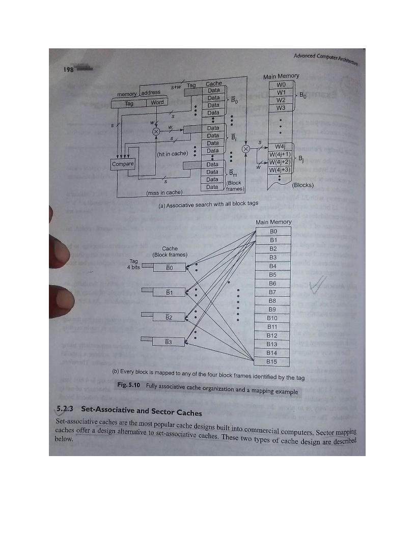
Ö CACHE MEMORY:
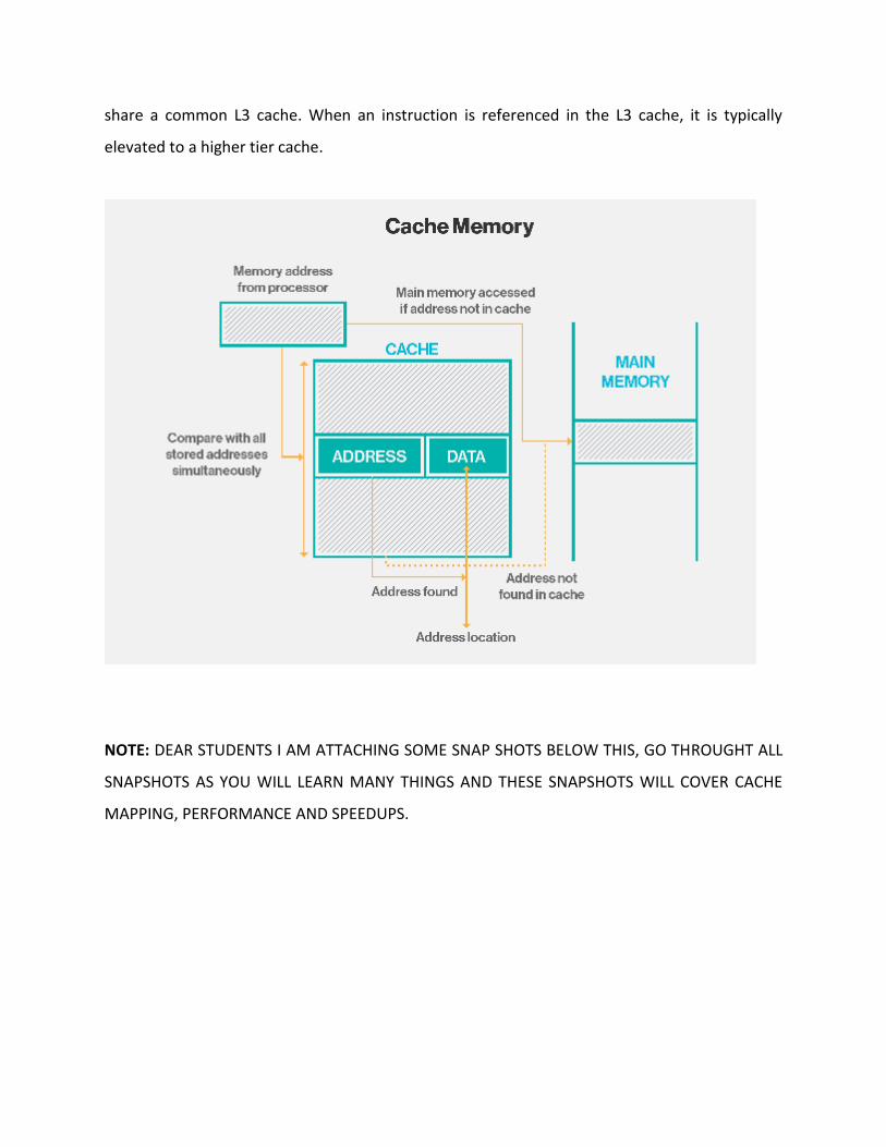
These are small fast memories placed between the processor and the main memory. Cache are
faster than the main memory, the cache are faster yet very expensive memories and are used
in only small sizes. Example cache of sizes 128KB, 256KB etc. are normally used in typical
Pentium based systems. Whereas they can have 4 to 128MB RAMs or even more. Memory
cache is a portion of the high-speed static RAM (SRAM) and is effective because most programs
access the same data or instructions over and over. By keeping as much of this information as
possible in SRAM, the computer avoids accessing the slower DRAM, making the computer
perform faster and more efficiently. Today, most computers come with L3 cache or L2 cache,
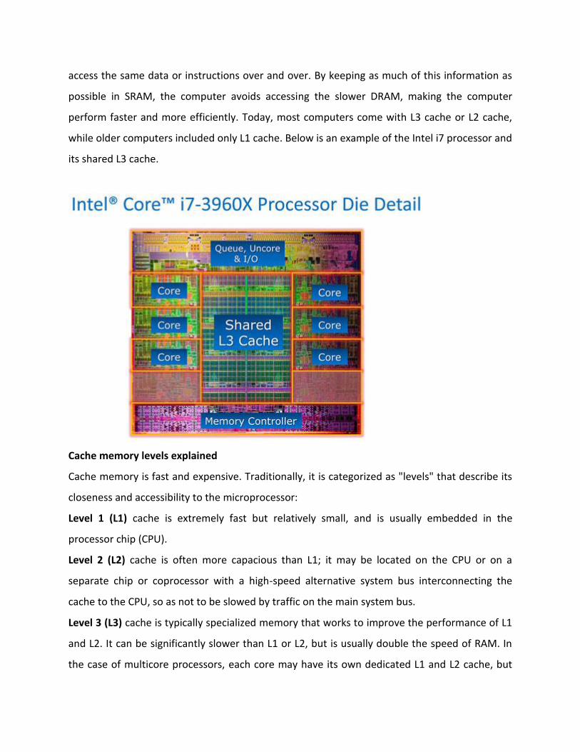
while older computers included only L1 cache. Below is an example of the Intel i7 processor and
its shared L3 cache.
Cache memory levels explained
Cache memory is fast and expensive. Traditionally, it is categorized as "levels" that describe its
closeness and accessibility to the microprocessor:
Level 1 (L1) cache is extremely fast but relatively small, and is usually embedded in the
processor chip (CPU).
Level 2 (L2) cache is often more capacious than L1; it may be located on the CPU or on a
separate chip or coprocessor with a high-speed alternative system bus interconnecting the
cache to the CPU, so as not to be slowed by traffic on the main system bus.
Level 3 (L3) cache is typically specialized memory that works to improve the performance of L1
and L2. It can be significantly slower than L1 or L2, but is usually double the speed of RAM. In
the case of multicore processors, each core may have its own dedicated L1 and L2 cache, but
share a common L3 cache. When an instruction is referenced in the L3 cache, it is typically
elevated to a higher tier cache.
NOTE: DEAR STUDENTS I AM ATTACHING SOME SNAP SHOTS BELOW THIS, GO THROUGHT ALL
SNAPSHOTS AS YOU WILL LEARN MANY THINGS AND THESE SNAPSHOTS WILL COVER CACHE
MAPPING, PERFORMANCE AND SPEEDUPS.
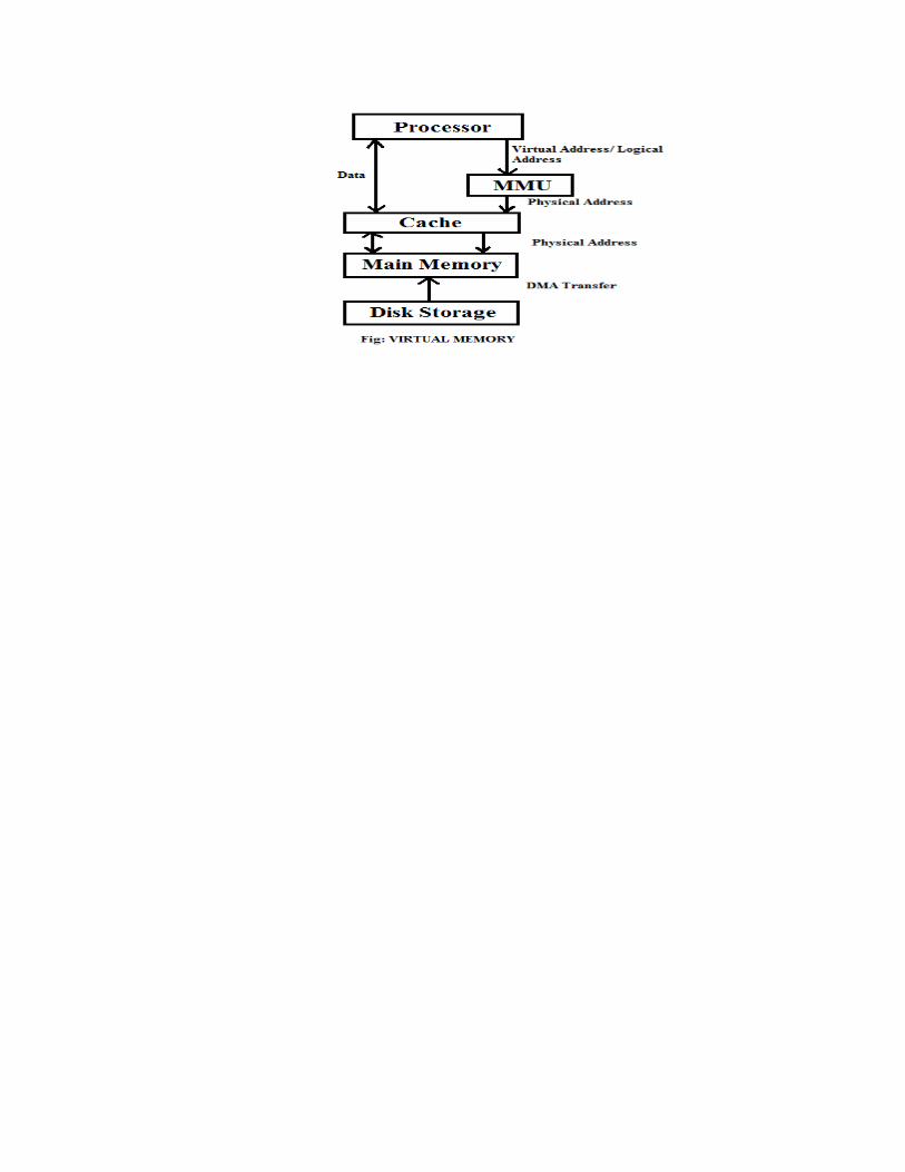
Ö Lecture 28 VIRTUAL MEMORIES: In most modern computer systems, the physical main
memory is not as large as the address space spanned by an address issued by the processor.
When a program does not completely fit into the main memory, the parts of it is not
currently being executed are stored in secondary storage devices, such as magnetic disks.
Off course all parts of a program that are eventually executed are brought first into the
main memory. When a new segment of a program is to be moved into a full memory. It
must replace another segment already in the memory. In modern computers the operating
system move programs and data automatically between the main memory and secondary
storage.
Techniques that automatically move program and data blocks into the physical main
memory when they are required for execution are called virtual memory techniques. The
binary address that the processor issues for either instructions or data are called virtual or
logical addresses. These addresses are translated into physical addresses by a combination
of hardware and software components.
Figure below shows a typical organization that implements virtual memory. A special
hardware unit called the memory management unit MMU translates virtual addresses into
physical addresses. When the desired data or instructions are in the main memory. If the
data is not in the main memory the MMU causes the operating system to bring the data
into the memory from the disk. Transfer of data between the disk and the main memory is
performed using the DMA (Direct Memory Access) scheme.


![Computer Architecture - Weebly...1 [RISC AND CISC] RISC AND CISC Generali 1. The dominant architecture in the PC market, the Intel IA-32, belongs to the Complex Instruction Set Computer](https://img.pdfslide.us/doc/110x75/60d6345cb801a56cc5222cad/computer-architecture-weebly-1-risc-and-cisc-risc-and-cisc-generali-1-the.jpg)