Embed Size (px)
Citation preview
Scaling to the Final Frontier:
Reliability challenges in sub 20 nm
TechnologiesTanya Nigam
Principal Member of Technical Staff
Technology Reliability Development
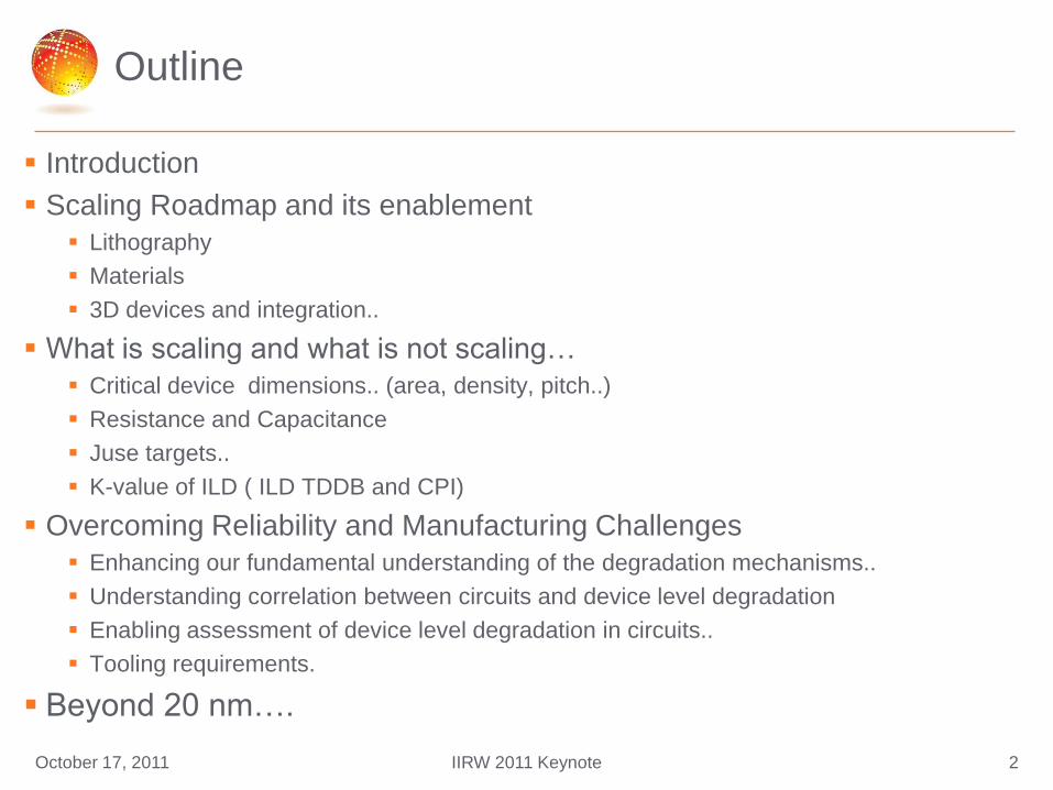
Outline
Introduction
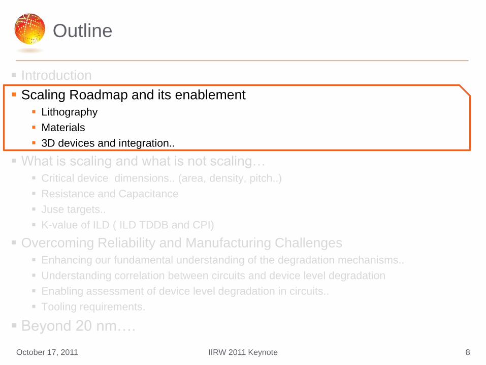
Scaling Roadmap and its enablement
Lithography
Materials
3D devices and integration..
What is scaling and what is not scaling…
Critical device dimensions.. (area, density, pitch..)
Resistance and Capacitance
Juse targets..
K-value of ILD ( ILD TDDB and CPI)
Overcoming Reliability and Manufacturing Challenges
Enhancing our fundamental understanding of the degradation mechanisms..
Understanding correlation between circuits and device level degradation
Enabling assessment of device level degradation in circuits..
Tooling requirements.
Beyond 20 nm….
October 17, 2011 2IIRW 2011 Keynote
Outline
Introduction
Scaling Roadmap and its enablement
Lithography
Materials
3D devices and integration..
What is scaling and what is not scaling…
Critical device dimensions.. (area, density, pitch..)
Resistance and Capacitance
Juse targets..
K-value of ILD ( ILD TDDB and CPI)
Overcoming Reliability and Manufacturing Challenges
Enhancing our fundamental understanding of the degradation mechanisms..
Understanding correlation between circuits and device level degradation
Enabling assessment of device level degradation in circuits..
Tooling requirements.
Beyond 20 nm….
October 17, 2011 3IIRW 2011 Keynote
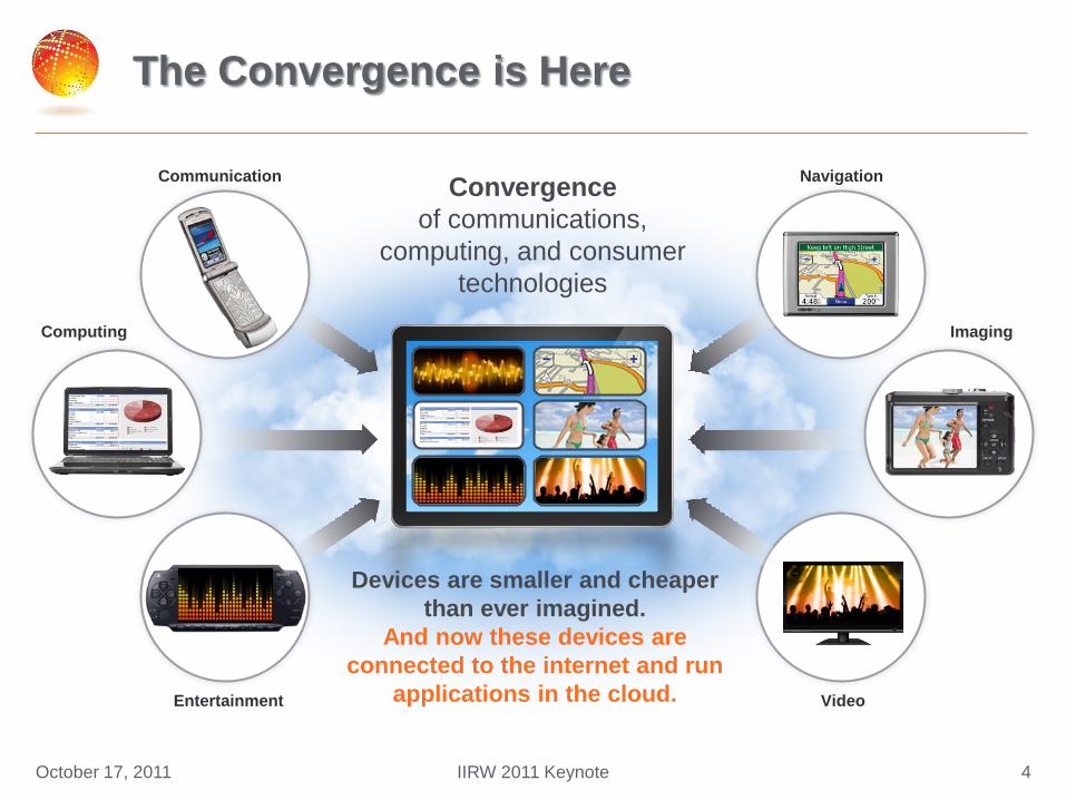
The Convergence is Here
Communication
Computing
Entertainment
Navigation
Imaging
Video
Devices are smaller and cheaper
than ever imagined.
And now these devices are
connected to the internet and run
applications in the cloud.
Convergence
of communications,
computing, and consumer
technologies
October 17, 2011 4IIRW 2011 Keynote
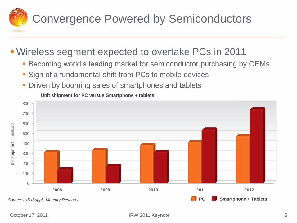
Convergence Powered by Semiconductors
Wireless segment expected to overtake PCs in 2011 Becoming world‘s leading market for semiconductor purchasing by OEMs
Sign of a fundamental shift from PCs to mobile devices
Driven by booming sales of smartphones and tablets
Source: IHS iSuppli, Mercury Research
0
100
200
300
400
500
600
700
800
2008 2009 2010 2011 2012
Unit shipment for PC versus Smartphone + tablets
PC Smartphone + Tablets
Unit s
hip
ment in
mill
ions
October 17, 2011 5IIRW 2011 Keynote
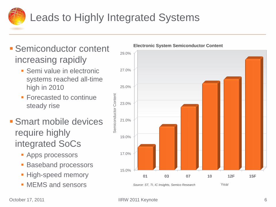
Leads to Highly Integrated Systems
Semiconductor content
increasing rapidly Semi value in electronic
systems reached all-time
high in 2010
Forecasted to continue
steady rise
Smart mobile devices
require highly
integrated SoCs Apps processors
Baseband processors
High-speed memory
MEMS and sensors
15.0%
17.0%
19.0%
21.0%
23.0%
25.0%
27.0%
29.0%
01 03 07 10 12F 15F
Source: ST, TI, IC Insights, Semico Research
Electronic System Semiconductor Content
Sem
iconducto
r C
onte
nt
Year
October 17, 2011 6IIRW 2011 Keynote
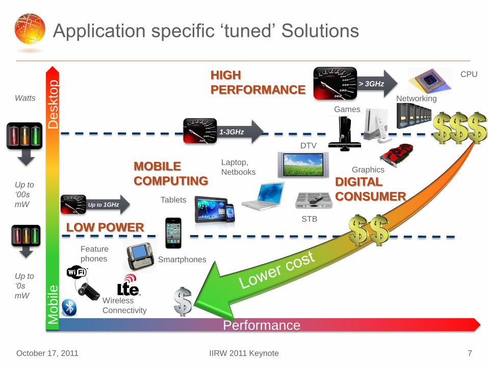
Application specific ‗tuned‘ Solutions
PerformanceMo
bile
De
skto
p
Tablets
MOBILE
COMPUTING DIGITAL
CONSUMER
Laptop,
Netbooks
Wireless
Connectivity
Feature
phones Smartphones
LOW POWER
Up to 1GHz
1-3GHz
STB
DTV
Graphics
Games
NetworkingWatts
Up to
‘00s
mW
Up to
‘0s
mW
CPUHIGH
PERFORMANCE> 3GHz
October 17, 2011 7IIRW 2011 Keynote
Outline
Introduction
Scaling Roadmap and its enablement
Lithography
Materials
3D devices and integration..
What is scaling and what is not scaling…
Critical device dimensions.. (area, density, pitch..)
Resistance and Capacitance
Juse targets..
K-value of ILD ( ILD TDDB and CPI)
Overcoming Reliability and Manufacturing Challenges
Enhancing our fundamental understanding of the degradation mechanisms..
Understanding correlation between circuits and device level degradation
Enabling assessment of device level degradation in circuits..
Tooling requirements.
Beyond 20 nm….
October 17, 2011 8IIRW 2011 Keynote
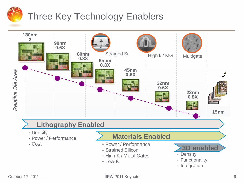
Three Key Technology EnablersR
ela
tive D
ie A
rea
90nm0.6X
80nm0.8X 65nm
0.8X45nm0.6X
32nm0.6X
130nmX
22nm0.8X
Strained Si High k / MG Multigate
15nm
Lithography Enabled
Materials Enabled
3D enabled
• Density
• Power / Performance
• Cost • Power / Performance
• Strained Silicon
• High K / Metal Gates
• Low-K
• Density
• Functionality
• Integration
October 17, 2011 9IIRW 2011 Keynote
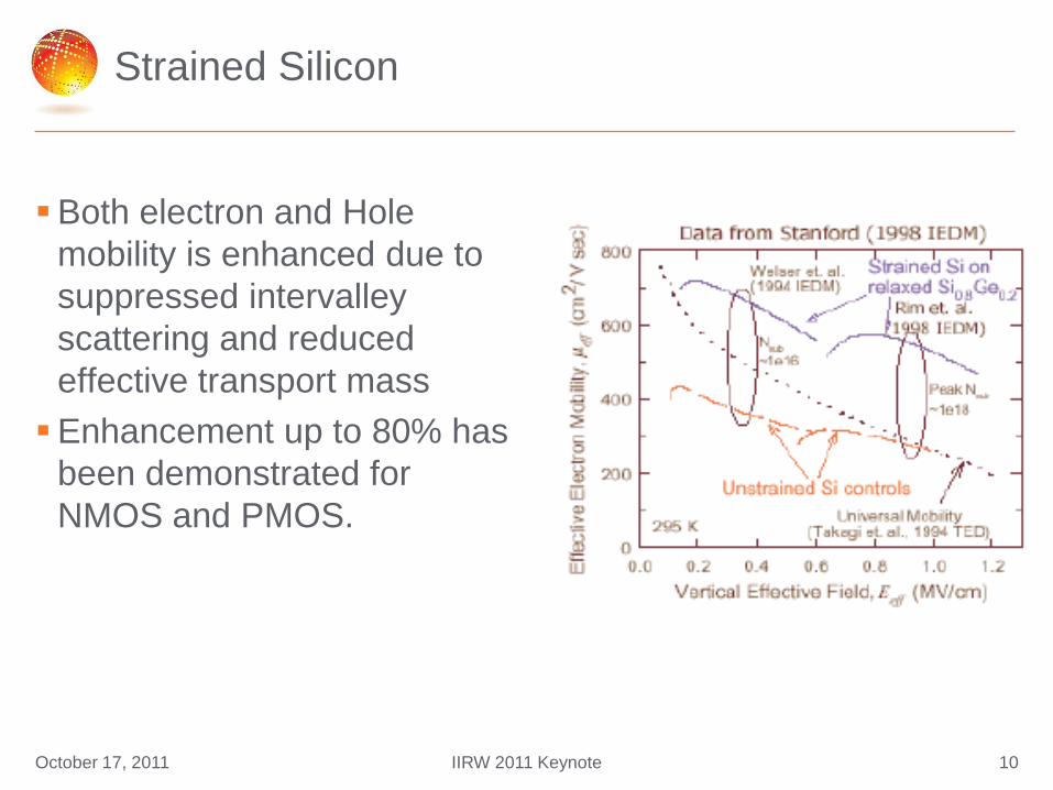
Strained Silicon
Both electron and Hole
mobility is enhanced due to
suppressed intervalley
scattering and reduced
effective transport mass
Enhancement up to 80% has
been demonstrated for
NMOS and PMOS.
October 17, 2011 10IIRW 2011 Keynote
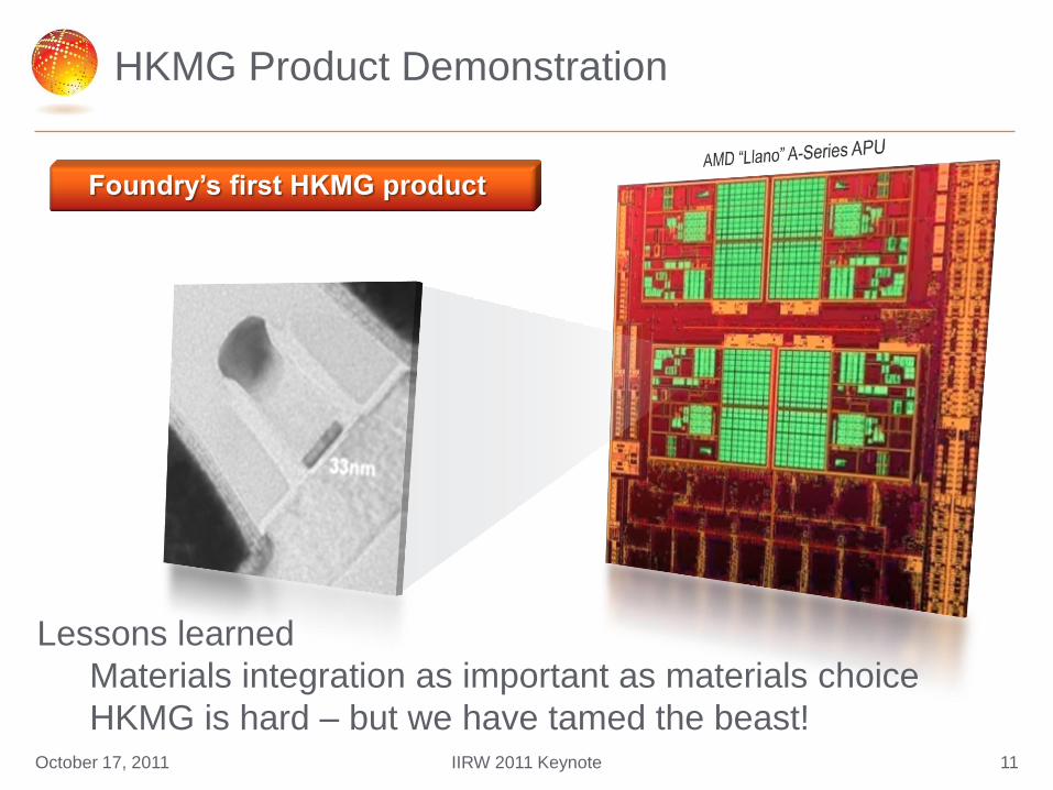
HKMG Product Demonstration
Foundry’s first HKMG product
Lessons learned
Materials integration as important as materials choice
HKMG is hard – but we have tamed the beast!October 17, 2011 11IIRW 2011 Keynote
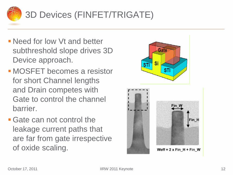
3D Devices (FINFET/TRIGATE)
Need for low Vt and better
subthreshold slope drives 3D
Device approach.
MOSFET becomes a resistor
for short Channel lengths
and Drain competes with
Gate to control the channel
barrier.
Gate can not control the
leakage current paths that
are far from gate irrespective
of oxide scaling.
October 17, 2011 12IIRW 2011 Keynote
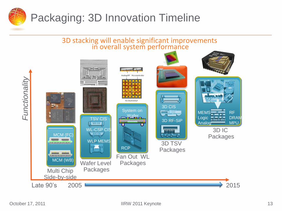
Packaging: 3D Innovation Timeline
2005 2015Late 90‘s
Fan Out WLPackages
3D IC Packages
MEMS
Logic
Analog
RF
DRAM
MPU
3D TSV Packages
3D RF-SiP
3D CIS
Wafer Level Packages
TSV CIS
WL-CSP CIS
WLP MEMS
RCP
System on
Wafer
MCM (WB)
Multi ChipSide-by-side
MCM (FC)
Fu
nctio
na
lity
3D stacking will enable significant improvementsin overall system performance
October 17, 2011 13IIRW 2011 Keynote
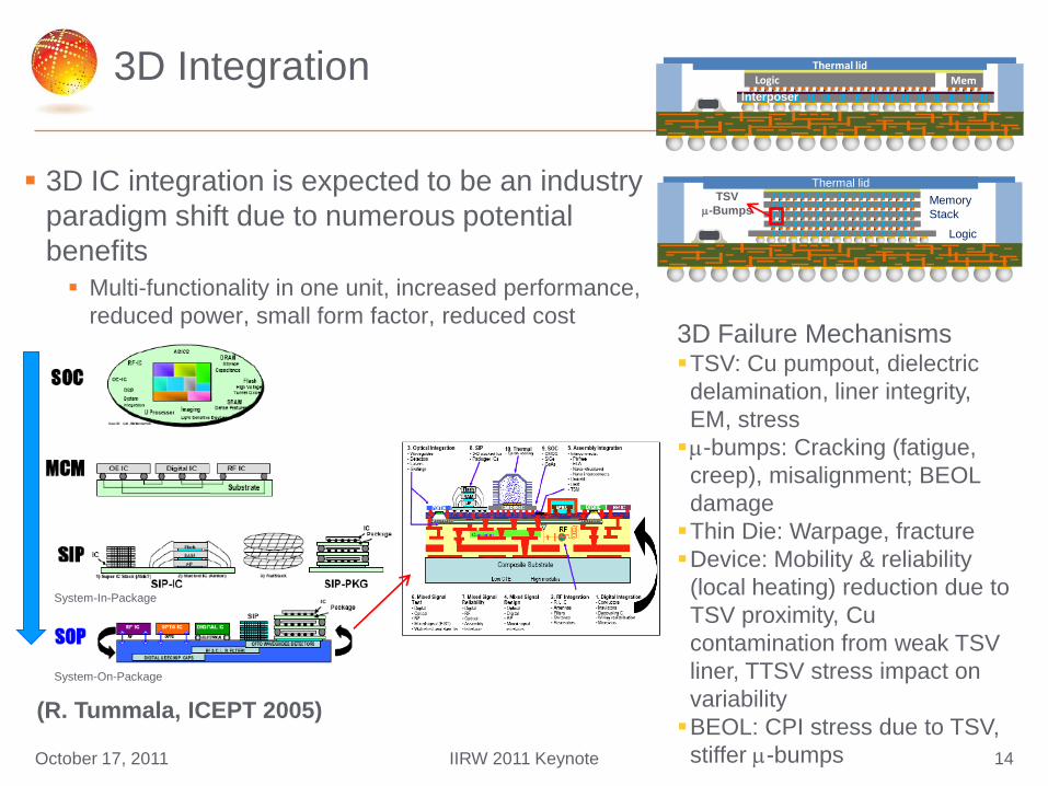
TSV
m-Bumps
3D Integration
3D IC integration is expected to be an industry
paradigm shift due to numerous potential
benefits
Multi-functionality in one unit, increased performance,
reduced power, small form factor, reduced cost
14
Thermal lid
Logic
Memory
Stack
MemLogic
Thermal lid
Interposer
3D Failure MechanismsTSV: Cu pumpout, dielectric
delamination, liner integrity,
EM, stress
m-bumps: Cracking (fatigue,
creep), misalignment; BEOL
damage
Thin Die: Warpage, fracture
Device: Mobility & reliability
(local heating) reduction due to
TSV proximity, Cu
contamination from weak TSV
liner, TTSV stress impact on
variability
BEOL: CPI stress due to TSV,
stiffer m-bumps
(R. Tummala, ICEPT 2005)
October 17, 2011 IIRW 2011 Keynote
System-On-Package
System-In-Package
Outline
Introduction
Scaling Roadmap and its enablement
Lithography
Materials
3D devices and integration..
What is scaling and what is not scaling…
Critical device dimensions.. (area, density, pitch..)
BEoL Resistance and Capacitance
Juse targets
K-value of ILD ( ILD TDDB and CPI)
Overcoming Reliability and Manufacturing Challenges
Enhancing our fundamental understanding of the degradation mechanisms..
Understanding correlation between circuits and device level degradation
Enabling assessment of device level degradation in circuits..
Tooling requirements.
Beyond 20 nm….
October 17, 2011 15IIRW 2011 Keynote
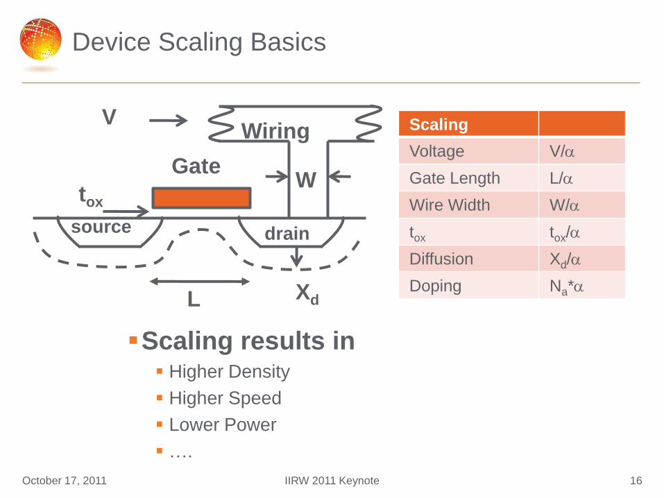
Device Scaling Basics
Scaling
Voltage V/a
Gate Length L/a
Wire Width W/a
tox tox/a
Diffusion Xd/a
Doping Na*a
Scaling results in Higher Density
Higher Speed
Lower Power
….
October 17, 2011 16IIRW 2011 Keynote
Gate
source drain
Wiring
W
XdL
tox
V
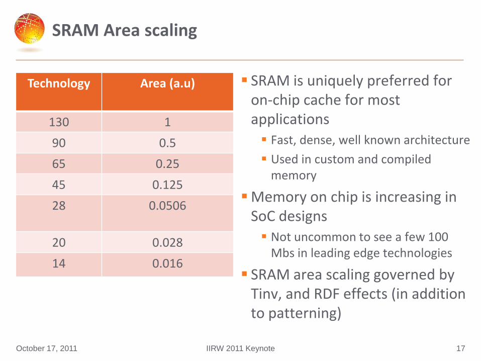
SRAM Area scaling
Technology Area (a.u)
130 1
90 0.5
65 0.25
45 0.125
28 0.0506
20 0.028
14 0.016
SRAM is uniquely preferred for on-chip cache for most applications Fast, dense, well known architecture
Used in custom and compiled memory
Memory on chip is increasing in SoC designs Not uncommon to see a few 100
Mbs in leading edge technologies
SRAM area scaling governed by Tinv, and RDF effects (in addition to patterning)
October 17, 2011 17IIRW 2011 Keynote
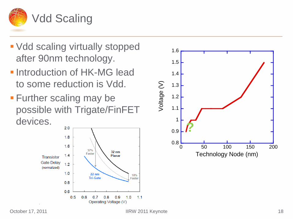
Vdd Scaling
Vdd scaling virtually stopped
after 90nm technology.
Introduction of HK-MG lead
to some reduction is Vdd.
Further scaling may be
possible with Trigate/FinFET
devices.
October 17, 2011 18IIRW 2011 Keynote
0.8
0.9
1
1.1
1.2
1.3
1.4
1.5
1.6
0 50 100 150 200
Volta
ge (
V)
Technology Node (nm)
?
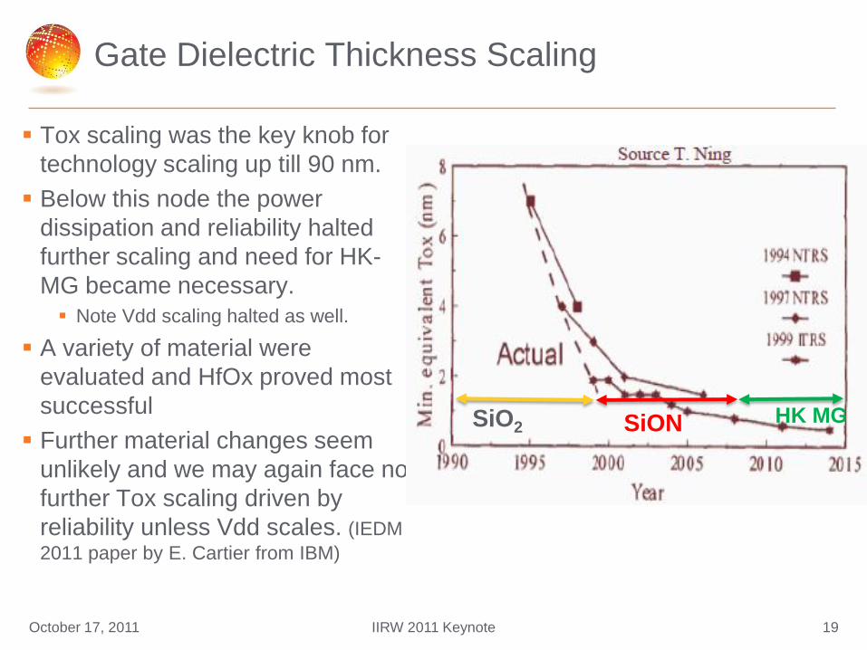
Gate Dielectric Thickness Scaling
Tox scaling was the key knob for
technology scaling up till 90 nm.
Below this node the power
dissipation and reliability halted
further scaling and need for HK-
MG became necessary.
Note Vdd scaling halted as well.
A variety of material were
evaluated and HfOx proved most
successful
Further material changes seem
unlikely and we may again face no
further Tox scaling driven by
reliability unless Vdd scales. (IEDM
2011 paper by E. Cartier from IBM)
October 17, 2011 19IIRW 2011 Keynote
HK MGSiO2 SiON
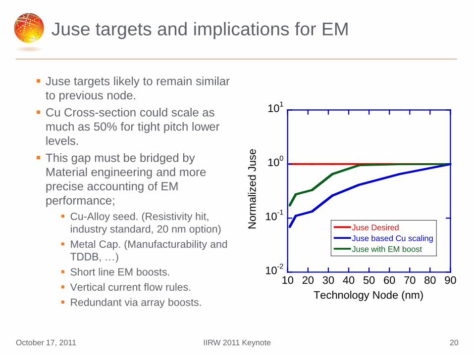
Juse targets and implications for EM
Juse targets likely to remain similar
to previous node.
Cu Cross-section could scale as
much as 50% for tight pitch lower
levels.
This gap must be bridged by
Material engineering and more
precise accounting of EM
performance;
Cu-Alloy seed. (Resistivity hit,
industry standard, 20 nm option)
Metal Cap. (Manufacturability and
TDDB, …)
Short line EM boosts.
Vertical current flow rules.
Redundant via array boosts.
10-2
10-1
100
101
10 20 30 40 50 60 70 80 90
Juse Desired
Juse based Cu scaling
Juse with EM boostN
orm
aliz
ed J
use
Technology Node (nm)
October 17, 2011 20IIRW 2011 Keynote
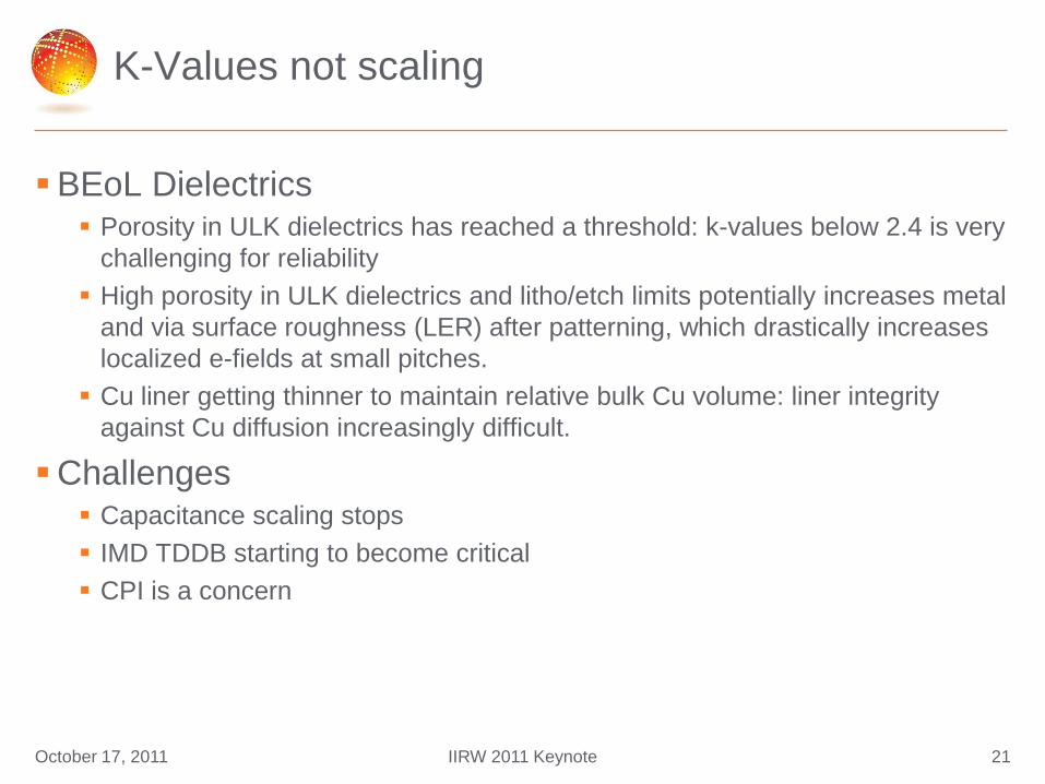
K-Values not scaling
BEoL Dielectrics Porosity in ULK dielectrics has reached a threshold: k-values below 2.4 is very
challenging for reliability
High porosity in ULK dielectrics and litho/etch limits potentially increases metal
and via surface roughness (LER) after patterning, which drastically increases
localized e-fields at small pitches.
Cu liner getting thinner to maintain relative bulk Cu volume: liner integrity
against Cu diffusion increasingly difficult.
Challenges Capacitance scaling stops
IMD TDDB starting to become critical
CPI is a concern
October 17, 2011 21IIRW 2011 Keynote
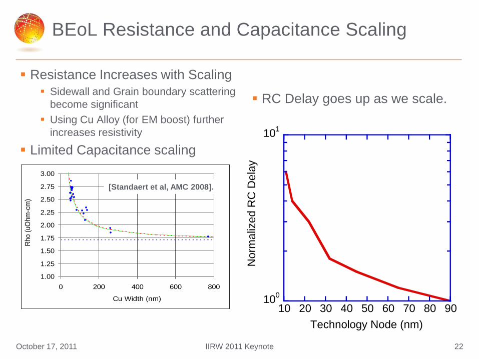
BEoL Resistance and Capacitance Scaling
Resistance Increases with Scaling
Sidewall and Grain boundary scattering
become significant
Using Cu Alloy (for EM boost) further
increases resistivity
Limited Capacitance scaling
1.00
1.25
1.50
1.75
2.00
2.25
2.50
2.75
3.00
0 200 400 600 800
Cu Width (nm)
Rho (
uO
hm
-cm
)
[Standaert et al, AMC 2008].
RC Delay goes up as we scale.
100
101
10 20 30 40 50 60 70 80 90
Norm
aliz
ed R
C D
ela
y
Technology Node (nm)
October 17, 2011 22IIRW 2011 Keynote
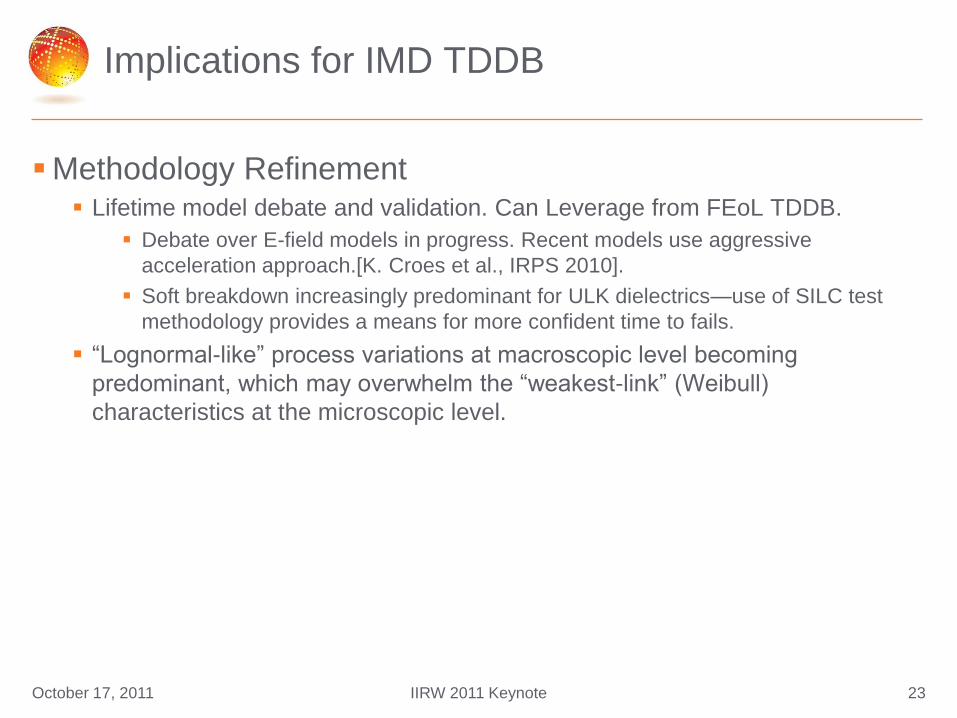
Implications for IMD TDDB
Methodology Refinement Lifetime model debate and validation. Can Leverage from FEoL TDDB.
Debate over E-field models in progress. Recent models use aggressive
acceleration approach.[K. Croes et al., IRPS 2010].
Soft breakdown increasingly predominant for ULK dielectrics—use of SILC test
methodology provides a means for more confident time to fails.
―Lognormal-like‖ process variations at macroscopic level becoming
predominant, which may overwhelm the ―weakest-link‖ (Weibull)
characteristics at the microscopic level.
October 17, 2011 23IIRW 2011 Keynote
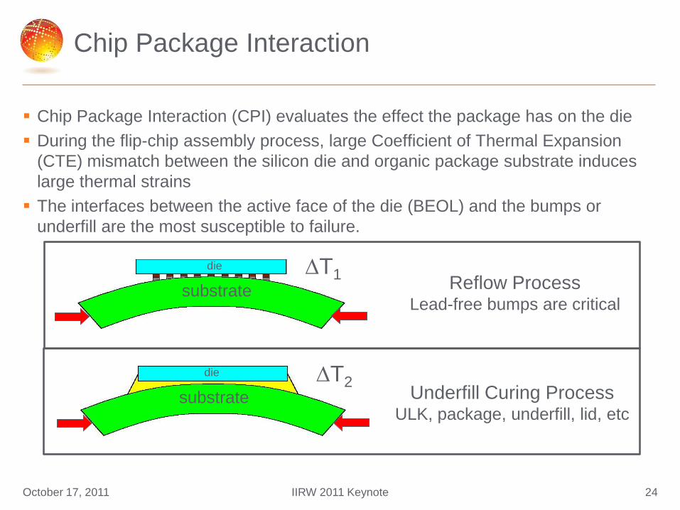
Chip Package Interaction
Chip Package Interaction (CPI) evaluates the effect the package has on the die
During the flip-chip assembly process, large Coefficient of Thermal Expansion
(CTE) mismatch between the silicon die and organic package substrate induces
large thermal strains
The interfaces between the active face of the die (BEOL) and the bumps or
underfill are the most susceptible to failure.
October 17, 2011 24IIRW 2011 Keynote
T2substrate
die
Underfill Curing ProcessULK, package, underfill, lid, etc
substrate
die T1Reflow Process
Lead-free bumps are critical
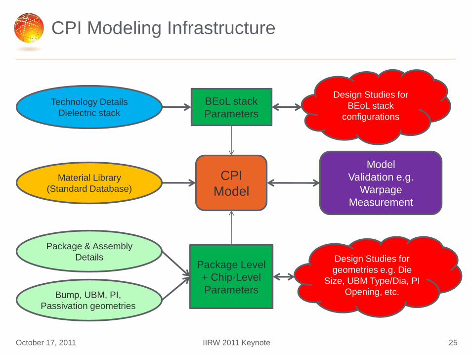
CPI Modeling Infrastructure
Technology Details
Dielectric stack
Material Library
(Standard Database)
Package & Assembly
Details
Bump, UBM, PI,
Passivation geometries
Package Level
+ Chip-Level
Parameters
BEoL stack
Parameters
25
Design Studies for
geometries e.g. Die
Size, UBM Type/Dia, PI
Opening, etc.
CPI
Model
Model
Validation e.g.
Warpage
Measurement
Design Studies for
BEoL stack
configurations
October 17, 2011 IIRW 2011 Keynote
Soft Errors
From Alpha particles (from radioactive impurities in Si/Package) & Cosmic
Rays (neutrons)
Dominant mechanism for SER in bulk CMOS is through direct charge
collection at transistor drains
Bulk technology 2-5x more sensitive than SOI technology
Impact of technology scaling: two competing trends
Smaller size/lower Vdd less node capacitance (less charge) increased vulnerability
Smaller size less area lower probability of strike
Overall, although feature size shrinks, the number of features grow, so the total system
area does not shrink
With tech node scaling, logic SER becoming comparable to SRAMs
SER susceptibility of latches will be similar to SRAMs, susceptibility of combinational
logic increasing rapidly
Correction schemes for SRAMs not feasible for latches due to their spatially distributed
nature
Circuit-level mitigation techniques for logic have high power, area and timing costs
October 17, 2011 26IIRW 2011 Keynote
Outline
Introduction
Scaling Roadmap and its enablement
Lithography
Materials
3D devices and integration..
What is scaling and what is not scaling…
Critical device dimensions.. (area, density, pitch..)
Resistance and Capacitance
Juse targets..
K-value of ILD ( ILD TDDB and CPI)
Overcoming Reliability and Manufacturing Challenges
Enhancing our fundamental understanding of the degradation mechanisms..
Understanding correlation between circuits and device level degradation
Enabling assessment of device level degradation in circuits..
Tooling requirements.
Beyond 20 nm….
27October 17, 2011 IIRW 2011 Keynote
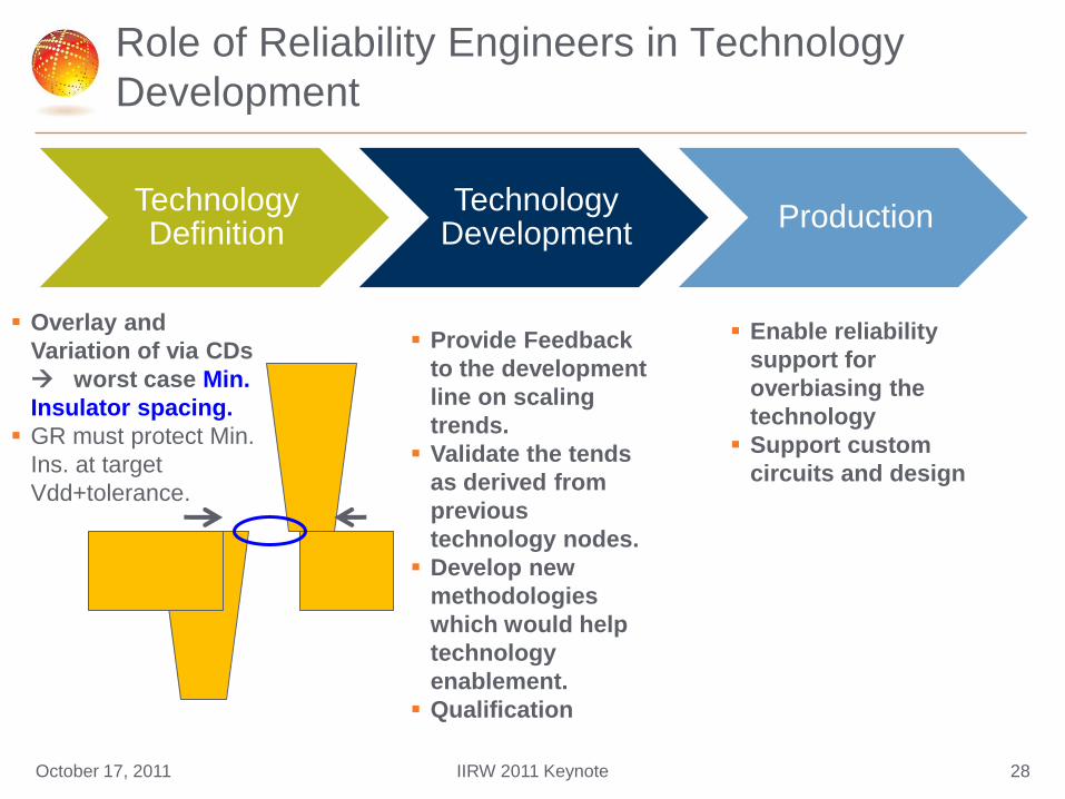
Role of Reliability Engineers in Technology
Development
Technology Definition
Technology Development
Production
October 17, 2011 28
Overlay and
Variation of via CDs
worst case Min.
Insulator spacing.
GR must protect Min.
Ins. at target
Vdd+tolerance.
Provide Feedback
to the development
line on scaling
trends.
Validate the tends
as derived from
previous
technology nodes.
Develop new
methodologies
which would help
technology
enablement.
Qualification
Enable reliability
support for
overbiasing the
technology
Support custom
circuits and design
IIRW 2011 Keynote
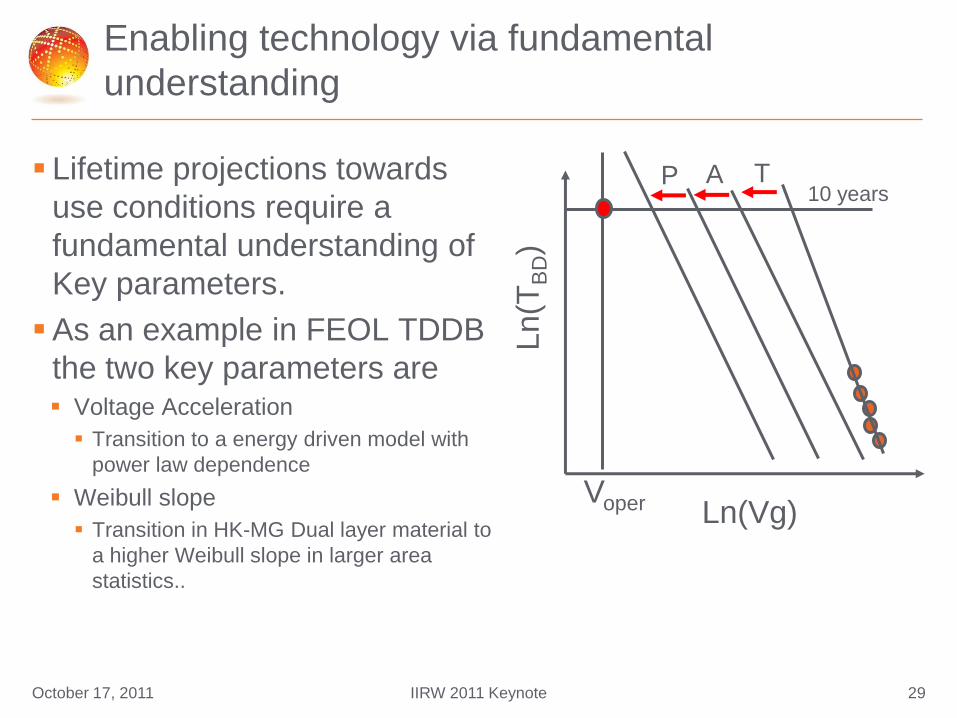
Enabling technology via fundamental
understanding
Lifetime projections towards
use conditions require a
fundamental understanding of
Key parameters.
As an example in FEOL TDDB
the two key parameters are Voltage Acceleration
Transition to a energy driven model with
power law dependence
Weibull slope
Transition in HK-MG Dual layer material to
a higher Weibull slope in larger area
statistics..
29
Ln(Vg)Ln(T
BD)
TAP
Voper
10 years
October 17, 2011 IIRW 2011 Keynote
IIRW 2011 Keynote
Oxide breakdown – Energy Driven
Lower TBD as Vsub is increased (No change in Eox or Istress)
Can not be explained by Eox model
Supports energy driven BD
T. Nigam, PhD Thesis 1999
Other Publications
Vogel et al. TED, 47, 1183, 2000
DiMaria, JAP, 86, 2100, 1999
Umrda et al. JAP, 82, 297,1997
October 17, 2011 30
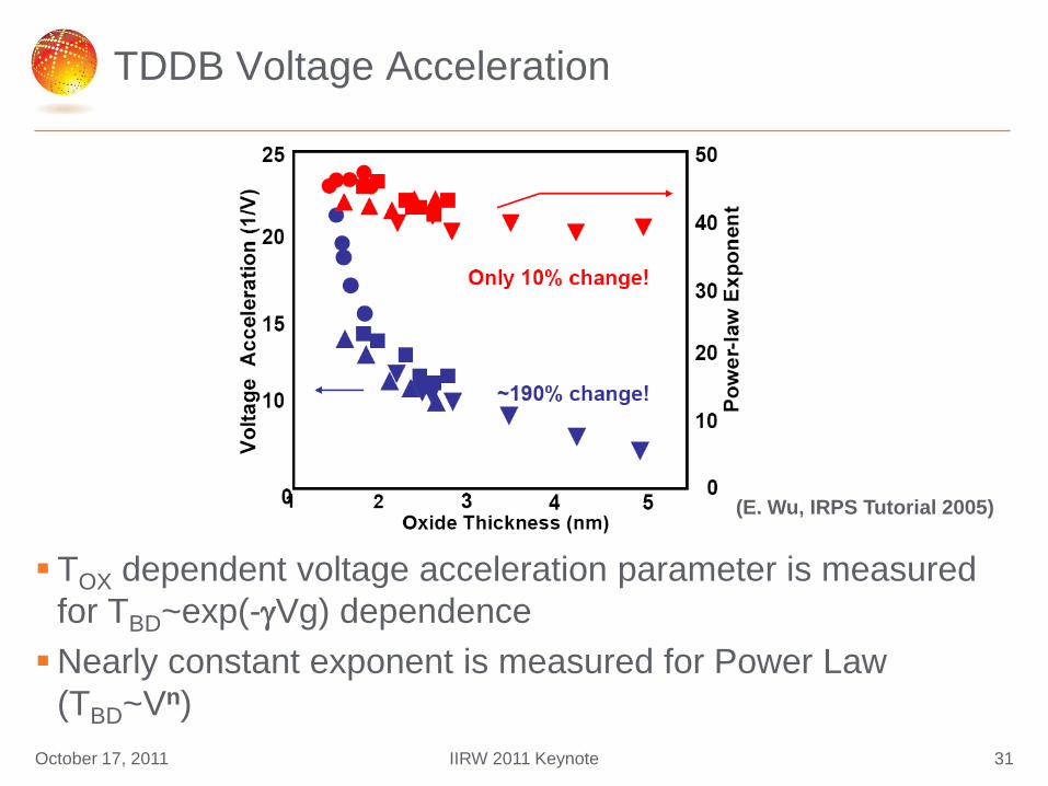
TDDB Voltage Acceleration
TOX dependent voltage acceleration parameter is measured
for TBD~exp(-gVg) dependence
Nearly constant exponent is measured for Power Law
(TBD~Vn)
(E. Wu, IRPS Tutorial 2005)
October 17, 2011 31IIRW 2011 Keynote
32
Basic TDDB Observations for HK
Significant SILC is measured on NFET during stress
Large number of defects are generated in HK.
In the literature, data is mostly collected on small areas
The obtained Weibull slope is limited by the interfacial oxide
Weibull slope increases with area for NMOS and PMOS
See Kerber, IRSP 2009
PFET Weibull slope is less than that of NFET
See Kerber IRPS 2009
Vertical area scaling works all the way to 1000mm2
Any theory proposed must explain all the above observations
October 17, 2011 32IIRW 2011 Keynote
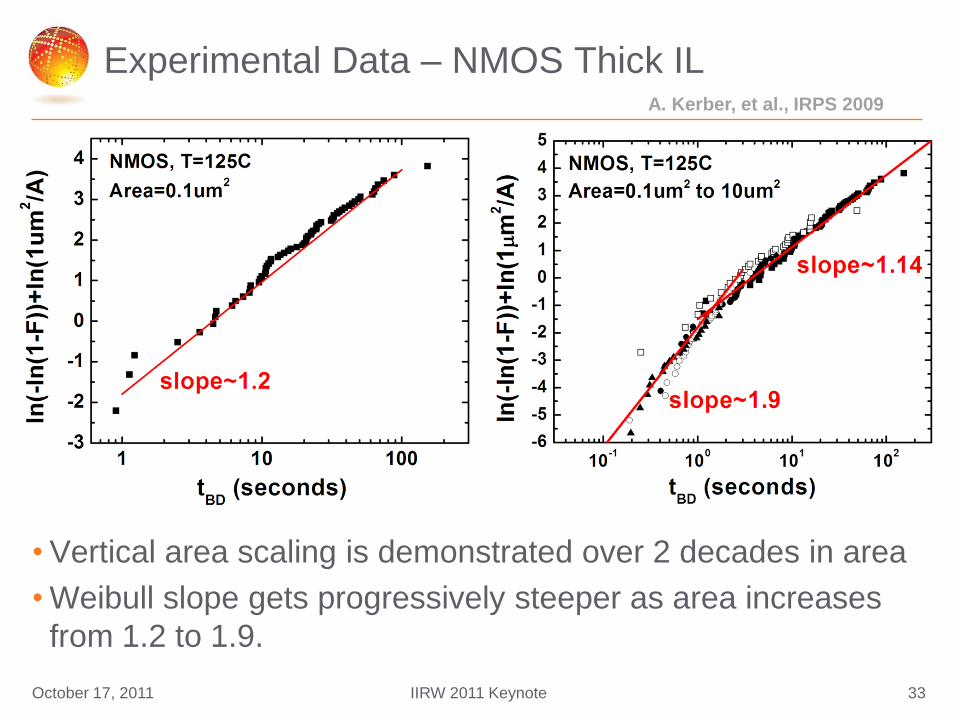
Experimental Data – NMOS Thick IL
• Vertical area scaling is demonstrated over 2 decades in area
• Weibull slope gets progressively steeper as area increases
from 1.2 to 1.9.
October 17, 2011 33IIRW 2011 Keynote
A. Kerber, et al., IRPS 2009
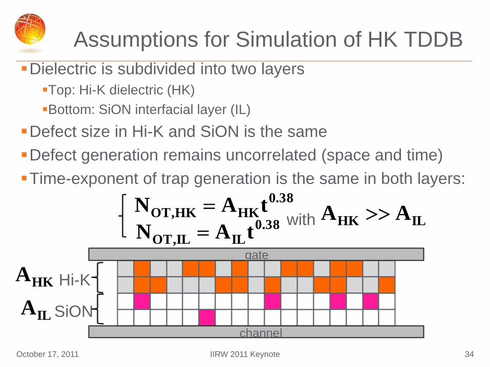
Dielectric is subdivided into two layers
Top: Hi-K dielectric (HK)
Bottom: SiON interfacial layer (IL)
Defect size in Hi-K and SiON is the same
Defect generation remains uncorrelated (space and time)
Time-exponent of trap generation is the same in both layers:
Assumptions for Simulation of HK TDDB
38.0HKHK,OT tAN
38.0ILIL,OT tAN
ILHK AA with
HKAgate
channel
Hi-K
SiONILA
October 17, 2011 34IIRW 2011 Keynote
gate
channel
Hi-K
SiON
gategategate
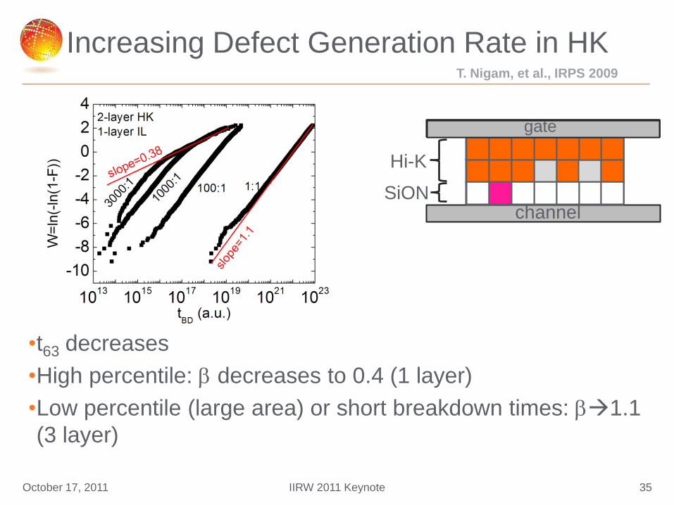
Increasing Defect Generation Rate in HK
•t63 decreases
•High percentile: decreases to 0.4 (1 layer)
•Low percentile (large area) or short breakdown times: 1.1
(3 layer)
October 17, 2011 35IIRW 2011 Keynote
T. Nigam, et al., IRPS 2009
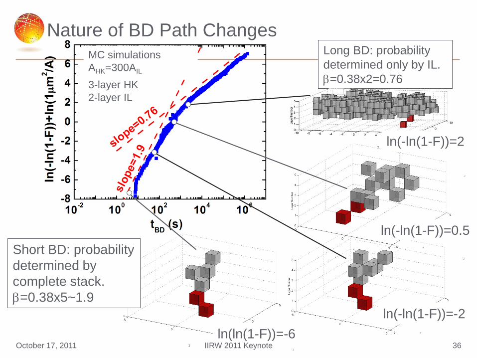
Short BD: probability
determined by
complete stack.
=0.38x5~1.9
ln(ln(1-F))=-6
ln(-ln(1-F))=-2
MC simulations
AHK=300AIL
Long BD: probability
determined only by IL.
=0.38x2=0.76
ln(-ln(1-F))=0.5
ln(-ln(1-F))=2
3-layer HK
2-layer IL
Nature of BD Path Changes
October 17, 2011 36IIRW 2011 Keynote
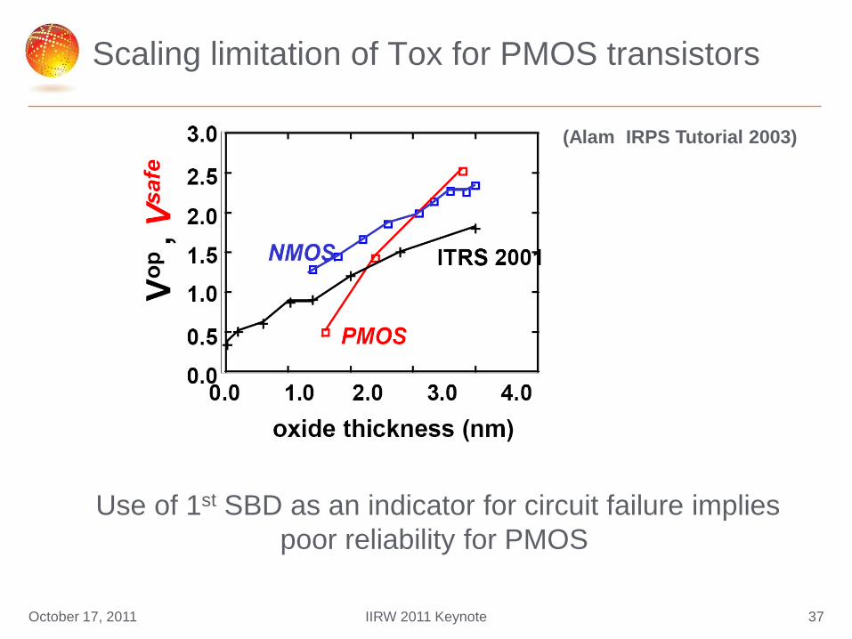
Scaling limitation of Tox for PMOS transistors
Use of 1st SBD as an indicator for circuit failure implies
poor reliability for PMOS
(Alam IRPS Tutorial 2003)
October 17, 2011 37IIRW 2011 Keynote
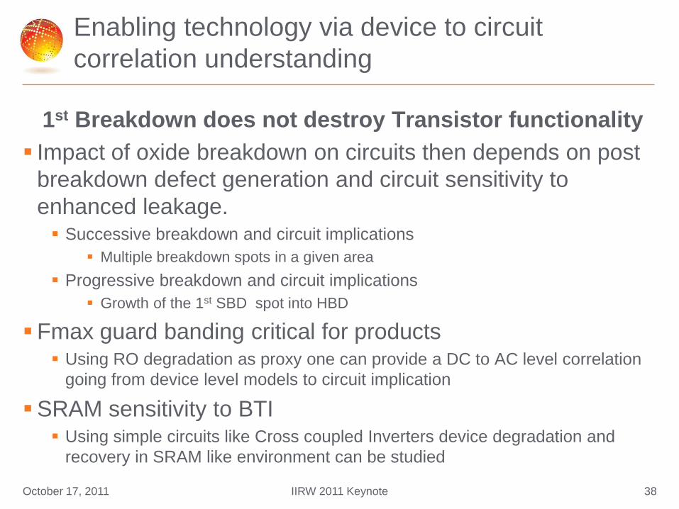
Enabling technology via device to circuit
correlation understanding
1st Breakdown does not destroy Transistor functionality
Impact of oxide breakdown on circuits then depends on post
breakdown defect generation and circuit sensitivity to
enhanced leakage. Successive breakdown and circuit implications
Multiple breakdown spots in a given area
Progressive breakdown and circuit implications
Growth of the 1st SBD spot into HBD
Fmax guard banding critical for products Using RO degradation as proxy one can provide a DC to AC level correlation
going from device level models to circuit implication
SRAM sensitivity to BTI Using simple circuits like Cross coupled Inverters device degradation and
recovery in SRAM like environment can be studied
October 17, 2011 38IIRW 2011 Keynote
0
10
20
30
0 100 200 300
Stress time (s)
off
IO
SC
(mA
) @
VO
SC
= 4
.4 V
1.55
1.60
1.65
1.70
f(M
Hz)
@ V
OS
C=
1.5
V
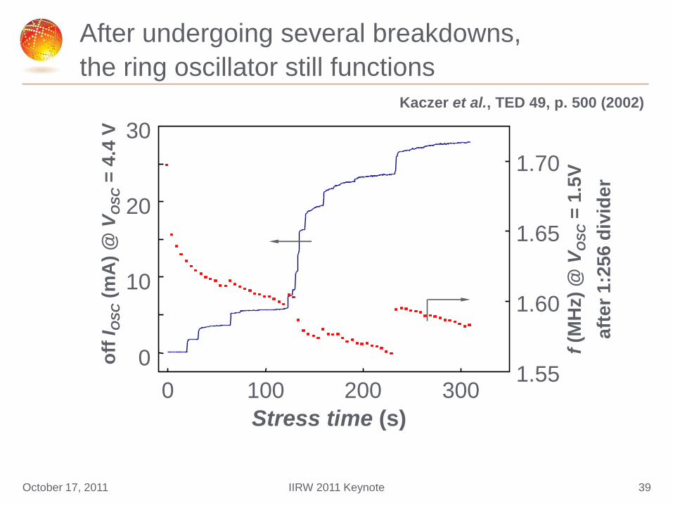
After undergoing several breakdowns,
the ring oscillator still functions
Kaczer et al., TED 49, p. 500 (2002)
aft
er
1:2
56
div
ide
r
October 17, 2011 39IIRW 2011 Keynote
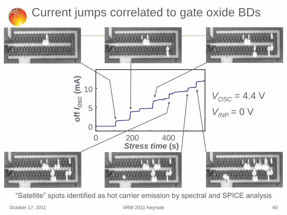
Current jumps correlated to gate oxide BDs
VOSC = 4.4 V
VINP = 0 V
0
5
10
0 200 400Stress time (s)
off
IO
SC
(mA
)
―Satellite‖ spots identified as hot carrier emission by spectral and SPICE analysis
October 17, 2011 40IIRW 2011 Keynote
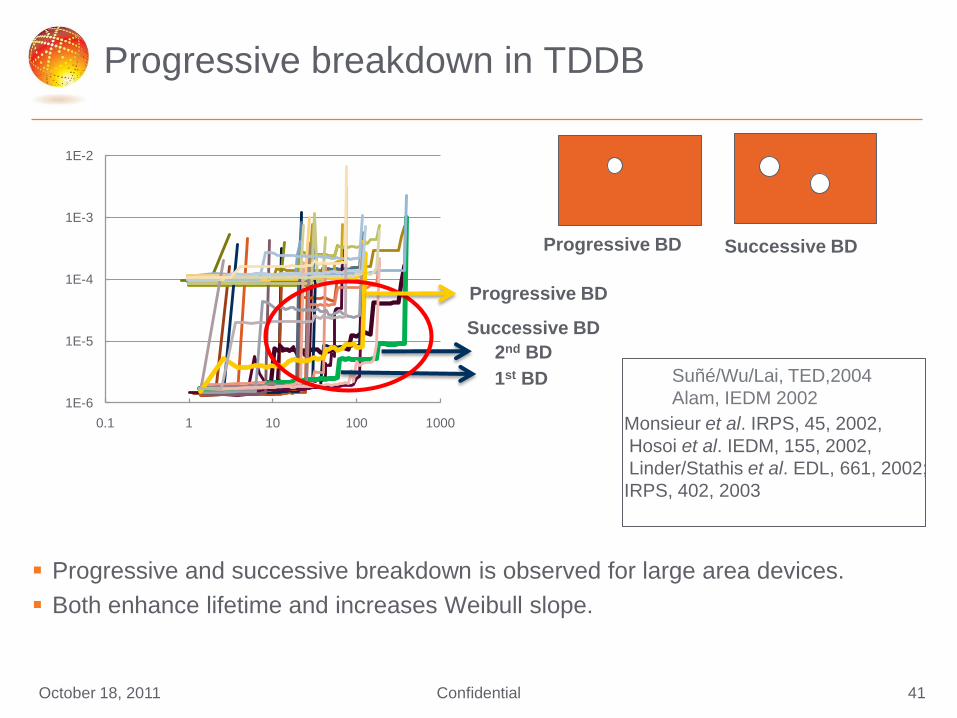
Progressive breakdown in TDDB
Progressive and successive breakdown is observed for large area devices.
Both enhance lifetime and increases Weibull slope.
1E-6
1E-5
1E-4
1E-3
1E-2
0.1 1 10 100 1000
1st BD
2nd BD
Progressive BD
Successive BD
Progressive BD Successive BD
October 18, 2011 41Confidential
Suñé/Wu/Lai, TED,2004
Alam, IEDM 2002
Monsieur et al. IRPS, 45, 2002,
Hosoi et al. IEDM, 155, 2002,
Linder/Stathis et al. EDL, 661, 2002;
IRPS, 402, 2003
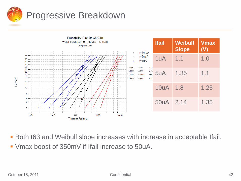
Progressive Breakdown
Both t63 and Weibull slope increases with increase in acceptable Ifail.
Vmax boost of 350mV if Ifail increase to 50uA.
October 18, 2011 42Confidential
Ifail Weibull
Slope
Vmax
(V)
1uA 1.1 1.0
5uA 1.35 1.1
10uA 1.8 1.25
50uA 2.14 1.35
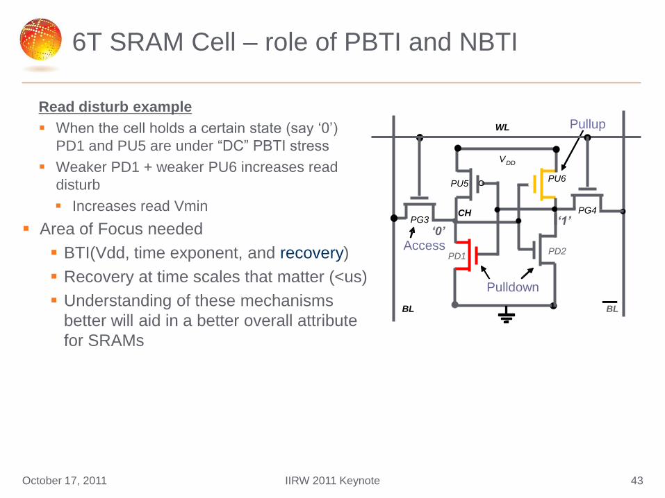
Read disturb example
When the cell holds a certain state (say ‗0‘)
PD1 and PU5 are under ―DC‖ PBTI stress
Weaker PD1 + weaker PU6 increases read
disturb
Increases read Vmin
Area of Focus needed
BTI(Vdd, time exponent, and recovery)
Recovery at time scales that matter (<us)
Understanding of these mechanisms
better will aid in a better overall attribute
for SRAMs
6T SRAM Cell – role of PBTI and NBTI
PD1
‘1’
PU5
WL
BL
PG3
Pulldown
Access
CH
‘0’
Pullup
PD2
PU6
BL
VDD
PG4
October 17, 2011 43IIRW 2011 Keynote
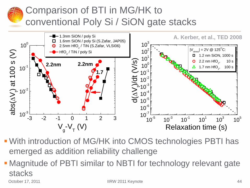
With introduction of MG/HK into CMOS technologies PBTI has
emerged as addition reliability challenge
Magnitude of PBTI similar to NBTI for technology relevant gate
stacks
-3 -2 -1 0 1 2 310
-3
10-2
10-1
100
2.2nm
1.7
1.3nm SiON / poly Si
1.6nm SiON / poly Si (S.Zafar, JAP05)
2.5nm HfO2 / TiN (S.Zafar, VLSI06)
HfO2 / TiN / poly Si
ab
s(
Vt) a
t 1
00
s (
V)
Vg-V
T (V)
2.2nm
A. Kerber, et al., TED 2008
Comparison of BTI in MG/HK to
conventional Poly Si / SiON gate stacks
10-5
10-3
10-1
101
103
105
10-7
10-6
10-5
10-4
10-3
10-2
10-1
100
101
102
103
|Vstress
| = 2V @ 125OC:
1.2 nm SiON, 1000 s
2.2 nm HfO2, 10 s
1.7 nm HfO2, 100 s
d(
Vt)/
dt (V
/s)
Relaxation time (s)
October 17, 2011 44IIRW 2011 Keynote
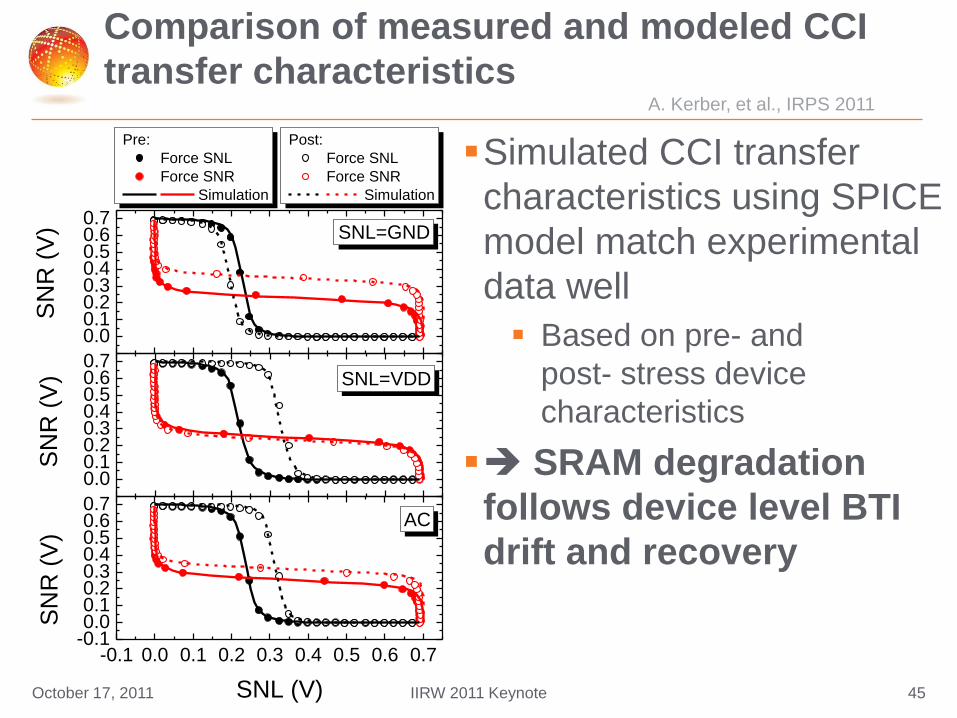
Comparison of measured and modeled CCI
transfer characteristics
Simulated CCI transfer
characteristics using SPICE
model match experimental
data well
Based on pre- and
post- stress device
characteristics
SRAM degradation
follows device level BTI
drift and recovery
-0.1 0.0 0.1 0.2 0.3 0.4 0.5 0.6 0.7-0.10.00.10.20.30.40.50.60.7
SNL=VDD
SNL=GND
SN
R (
V)
SN
R (
V)
SN
R (
V)
SNL (V)
AC
0.00.10.20.30.40.50.60.7
0.00.10.20.30.40.50.60.7
Post:
Force SNL
Force SNR
Simulation
Pre:
Force SNL
Force SNR
Simulation
A. Kerber, et al., IRPS 2011
October 17, 2011 45IIRW 2011 Keynote
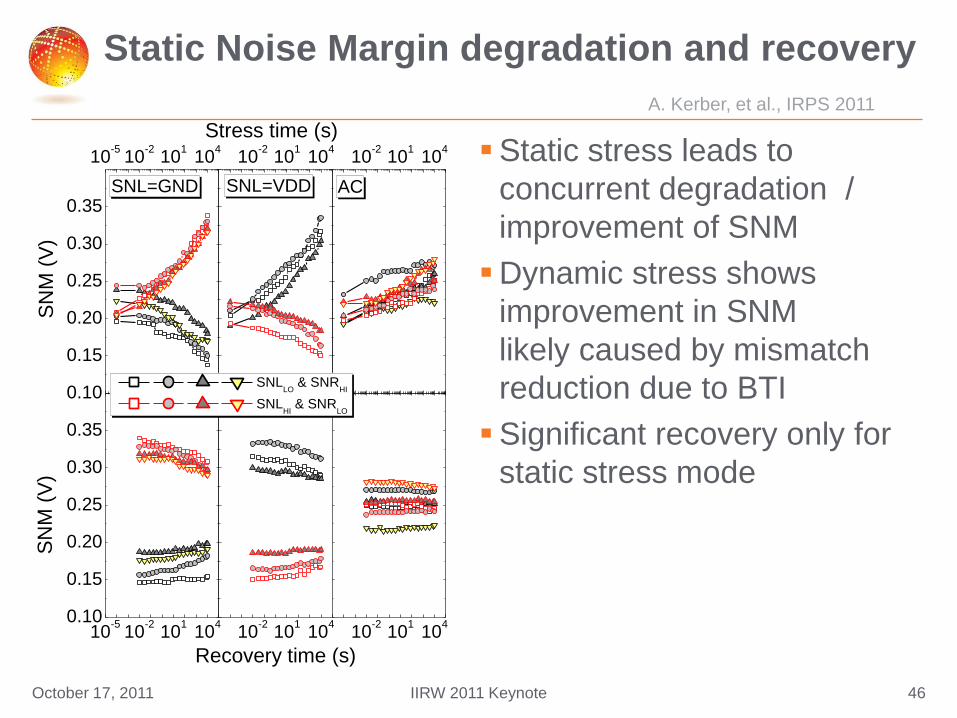
Static Noise Margin degradation and recovery
Static stress leads to
concurrent degradation /
improvement of SNM
Dynamic stress shows
improvement in SNM
likely caused by mismatch
reduction due to BTI
Significant recovery only for
static stress mode
0.10
0.15
0.20
0.25
0.30
0.35
10-5
10-2
101
104
SN
M (
V)
SNL=GND
10-2
101
104
Stress time (s)
10-2
101
104
SNL=VDD AC
10-5
10-2
101
104
0.10
0.15
0.20
0.25
0.30
0.35
SN
M (
V)
10-2
101
104
Recovery time (s)
10-2
101
104
SNLLO
& SNRHI
SNLHI
& SNRLO
A. Kerber, et al., IRPS 2011
October 17, 2011 46IIRW 2011 Keynote
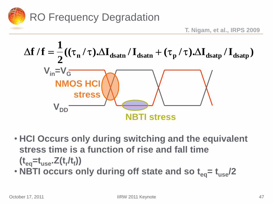
RO Frequency Degradation
)I/I)./(I/I)./((2
1f/f dsatpdsatppdsatndsatnn
Vin=VG
VDD
NBTI stress
NMOS HCI
stress
• HCI Occurs only during switching and the equivalent
stress time is a function of rise and fall time
(teq=tuse.Z(tr/tf))
• NBTI occurs only during off state and so teq= tuse/2
T. Nigam, et al., IRPS 2009
October 17, 2011 47IIRW 2011 Keynote
GlobalFoundries ConfidentialGlobalFoundries Confidential
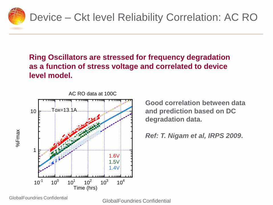
Device – Ckt level Reliability Correlation: AC RO
Ring Oscillators are stressed for frequency degradation
as a function of stress voltage and correlated to device
level model.
1
10
10-1
100
101
102
103
104
AC RO data at 100C
%F
max
Time (hrs)
Tox=13.1A
1.6V1.5V1.4V
Good correlation between data
and prediction based on DC
degradation data.
Ref: T. Nigam et al, IRPS 2009.
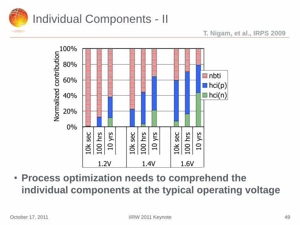
Individual Components - II
• Process optimization needs to comprehend the
individual components at the typical operating voltage
T. Nigam, et al., IRPS 2009
0%
20%
40%
60%
80%
100%
10k
sec
100 h
rs
10 y
rs
10k
sec
100 h
rs
10 y
rs
10k
sec
100 h
rs
10 y
rs
1.2V 1.4V 1.6V
Norm
aliz
ed c
ontr
ibution
nbti
hci(p)
hci(n)
October 17, 2011 49IIRW 2011 Keynote
Outline
Introduction
Scaling Roadmap and its enablement
Lithography
Materials
3D devices and integration..
What is scaling and what is not scaling…
Critical device dimensions.. (area, density, pitch..)
Resistance and Capacitance
Juse targets..
K-value of ILD ( ILD TDDB and CPI)
Overcoming Reliability and Manufacturing Challenges
Enhancing our fundamental understanding of the degradation mechanisms..
Understanding correlation between circuits and device level degradation
Enabling assessment of device level degradation in circuits..
Tooling requirements.
Beyond 20 nm….
October 17, 2011 50IIRW 2011 Keynote
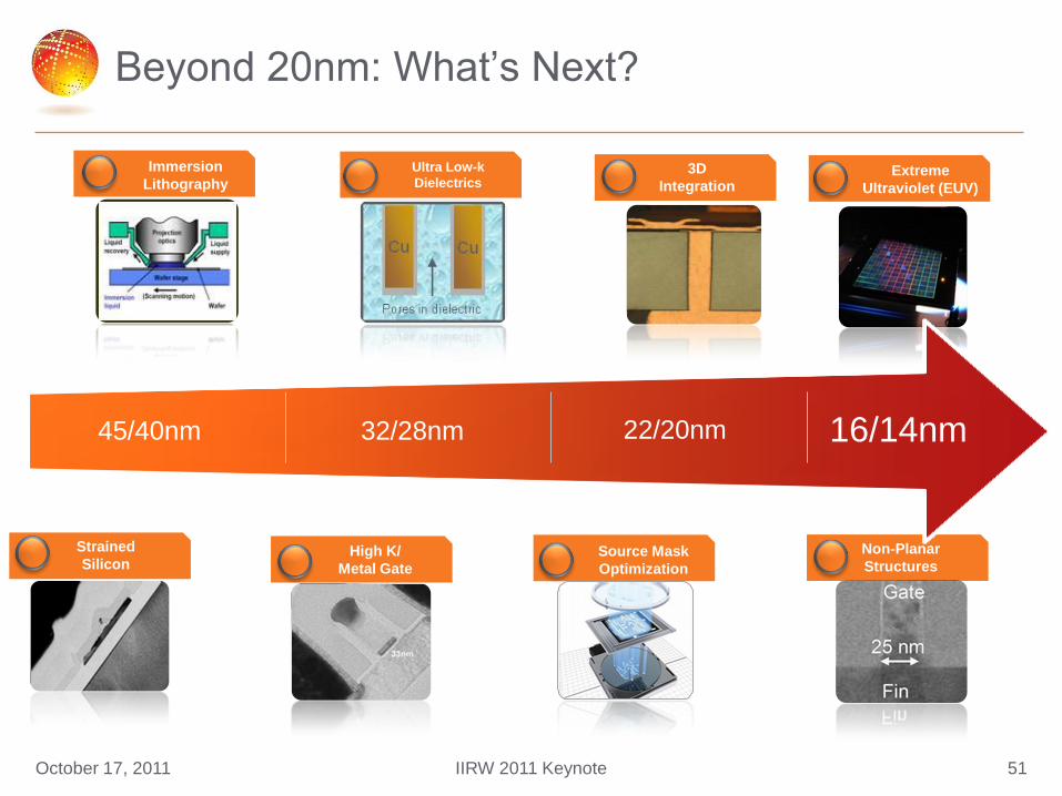
Beyond 20nm: What‘s Next?
Immersion
Lithography
Strained
Silicon
3D
IntegrationExtreme
Ultraviolet (EUV)
High K/
Metal Gate
Non-Planar
StructuresSource Mask
Optimization
Ultra Low-k
Dielectrics
32/28nm 16/14nm45/40nm 22/20nm
October 17, 2011 51IIRW 2011 Keynote
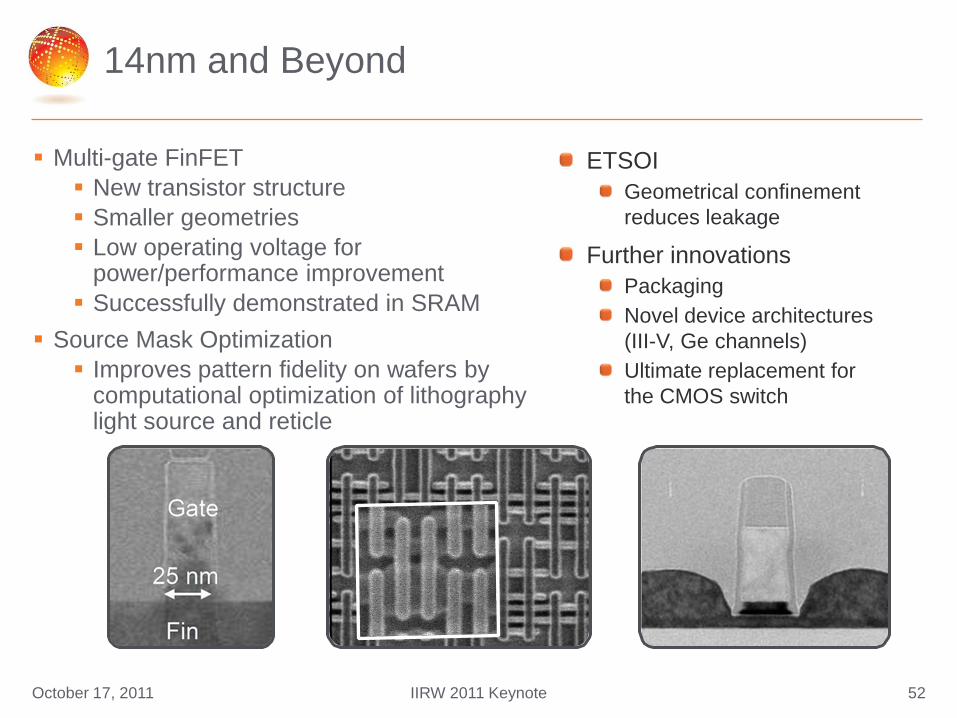
14nm and Beyond
Multi-gate FinFET
New transistor structure
Smaller geometries
Low operating voltage for power/performance improvement
Successfully demonstrated in SRAM
Source Mask Optimization
Improves pattern fidelity on wafers by computational optimization of lithography light source and reticle
ETSOI
Geometrical confinement
reduces leakage
Further innovations
Packaging
Novel device architectures
(III-V, Ge channels)
Ultimate replacement for
the CMOS switch
October 17, 2011 52IIRW 2011 Keynote
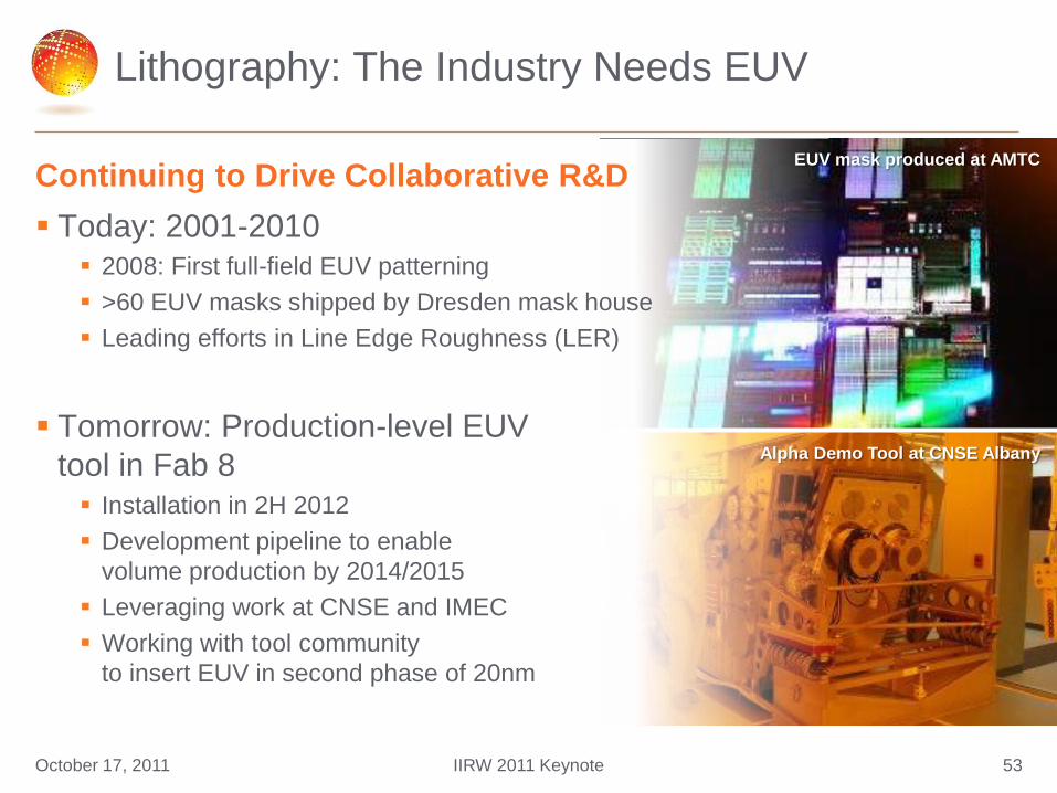
Lithography: The Industry Needs EUV
Continuing to Drive Collaborative R&D
Today: 2001-2010 2008: First full-field EUV patterning
>60 EUV masks shipped by Dresden mask house
Leading efforts in Line Edge Roughness (LER)
Tomorrow: Production-level EUV
tool in Fab 8 Installation in 2H 2012
Development pipeline to enable
volume production by 2014/2015
Leveraging work at CNSE and IMEC
Working with tool community
to insert EUV in second phase of 20nm
EUV mask produced at AMTC
Alpha Demo Tool at CNSE Albany
October 17, 2011 53IIRW 2011 Keynote
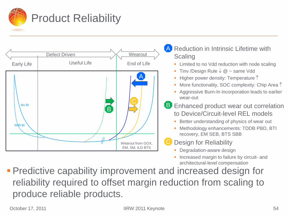
Product Reliability
Predictive capability improvement and increased design for
reliability required to offset margin reduction from scaling to
produce reliable products.
54
Reduction in Intrinsic Lifetime with
Scaling Limited to no Vdd reduction with node scaling
Tinv /Design Rule @ ~ same Vdd
Higher power density: Temperature
More functionality, SOC complexity: Chip Area
Aggressive Burn-In incorporation leads to earlier
wear-out
Enhanced product wear out correlation
to Device/Circuit-level REL models Better understanding of physics of wear out
Methodology enhancements: TDDB PBD, BTI
recovery, EM SEB, BTS SBB
Design for Reliability Degradation-aware design
Increased margin to failure by circuit- and
architectural-level compensation
A
B
C
A
C
Early Life Useful Life End of Life
Defect Driven Wearout
No BI
With BI
B
Wearout from GOX,
EM, SM, ILD BTS
October 17, 2011 IIRW 2011 Keynote
Summary
Semiconductor industry on path towards sub 20 nm
technology Key Challenges continue to be
Lithography
Material innovation and integration with an eye towards manufacturability
Building in Reliability Margins
Reliability Challenges Comprehend and model the impact of material change
Develop fundamental physical understanding
Leverage learning from other areas
Comprehend and link device level degradation to circuit level degradation
Provide designer with tools to build reliability aware designs
October 17, 2011 55IIRW 2011 Keynote
Acknowledgements
GLOBALFOUNDRIES FEOL Reliability Team A. Kerber, B. Parameshwaran, B. McMahon, ..
GLOBALFOUNDRIES BEOL Reliability Team P. Justison, Kok-Yong Yiang
GLOBALFOUNDRIES SRAM Team Srinath Krishnan, S. Balasubramanian
GLOBALFOUNDRIES Marketing Team Kelvin Low and Jason
ISDA Alliance Team in NY
October 17, 2011 56IIRW 2011 Keynote
Trademark Attribution
GLOBALFOUNDRIES, the GLOBALFOUNDRIES logo and combinations thereof are trademarks of GLOBALFOUNDRIES Inc. in the
United States and/or other jurisdictions. Other names used in this presentation are for identification purposes only and may be trademarks
of their respective owners.
©2011 GLOBALFOUNDRIES Inc. All rights reserved.
October 17, 2011 57IIRW 2011 Keynote