Embed Size (px)
Citation preview

10/30/2010
1
Dr. Ahmed H. Madian-VLSI 1
Very Large Scale Integration (VLSI)
Dr. Ahmed H. [email protected]
Lecture 6
Dr. Ahmed H. Madian-VLSI 2
Contents FPGA Technology
Programmable logic Cell (PLC)
Mux-based cells
Look up table
PLA
Programmable interconnection
Antifuse
SRAM
EPROM
Placement and Routing
Min-Cut
Simulated Annealing

10/30/2010
2
Dr. Ahmed H. Madian-VLSI 3
Field Programmable Gate Array (FPGA)
Programming technology
Programmable logic cells
Programmable interconnect
Anti fuse (One time programmable, ex. Actel)
Static RAM (volatile, ex. Xilinx)
EPROM or EEPROM (non-volatile, ex. Altera)
Programmable I/O‟s
Dr. Ahmed H. Madian-VLSI 4
Programmable Logic Cells
The logic cells could be programmed to realize a logic function the main blocks are:
Multiplexer based (ACTEL)
Look-up tables (XILINX)
AND-OR array (ALTERA)

10/30/2010
3
Dr. Ahmed H. Madian-VLSI 5
Programmable Logic Cells
Multiplexer Based logic cells
The logic function could be written using shanon‟s
expansion theorem:
01 ..,..),,( AA FAFACBAF
Dr. Ahmed H. Madian-VLSI 6
Programmable Logic Cells
Realize the following logic function using Multiplexer Based logic cells
DBCBAF ..

10/30/2010
4
Dr. Ahmed H. Madian-VLSI 7
Programmable Logic Cells
Multiplexer Based logic cells
).().(
1
).(..
DCBDABF
BBwhere
BBDBCBAF
FB=1 = A+D = A(1) + A(D)
FB=0 = C+D = C(1) + C(D)
Dr. Ahmed H. Madian-VLSI 8
Programmable Logic Cells
Multiplexer Based logic cells
Combinational module (C-module)
Sequential module (S-module)
(C-module) (S-module)

10/30/2010
5
Dr. Ahmed H. Madian-VLSI 9
Programmable Logic Cells
Layout of the 4x1 Mux using TG technology.
Not always compact layout, but you can make a nice Boolean Unit like in table below.
0
1
2
3
AB
I0
I1
I2
I3
O
Out(o)I0I1I2I3
Zero000 0
AND000 1
OR0111
XOR0110
Dr. Ahmed H. Madian-VLSI 10
Look-Up tables (LUT)
LUT mainly depends on RAM blocks
We could realize any logic function from truth table using RAM This is done by
mapping the inputs to the address bus
The output is mapped to the data bus

10/30/2010
6
Dr. Ahmed H. Madian-VLSI 11
LUT Simplified XC4000 CLB
Dr. Ahmed H. Madian-VLSI 12
FPGA (SLICE)
Slices (grouped into CLBs = Configurable
Logic Blocs)
• Contain combinatorial logic and register
resourcesFor example each Spartan™‐3 CLB contains
four slices:Slices are grouped in pairs
Left-hand SLICEM (Memory)
• LUTs can be configured as memory or
SRL16
Right-hand SLICEL (Logic)
• LUT Switch Matrix Slice can be used as logic
only.

10/30/2010
7
Dr. Ahmed H. Madian-VLSI 13
Programmable Logic Arrays (And-OR-Plane) (PLA)
It usually constructed directly from minimized Sum-Of-Product logic equations:
the rows represent the minterms of the equations, the “input” columns form the minterms and the “output”columns form the sums.
Note that with multiple output columns, minterm sharing between the outputs happens naturally
Address decoder implemented as
AND (= NOR)
For each Fi,
OR together
all rows for
which output
is 1 (actually
use NOR then
invert).
Dr. Ahmed H. Madian-VLSI 14
PLA Folding
PLAs can be sparse, i.e., only a few of the possible connections in either plane may be made. (AND plane can only have 50%!)
If we allow input and outputs to come from both above and below then we may be able to fold two columns into one if the rows they use don’t overlap. This may require rearranging the rows to minimize overlap and hence maximize folding possibilities.

10/30/2010
8
Dr. Ahmed H. Madian-VLSI 15
Multiple Input Encoding
On the previous slide, it was noted that the AND plane can have at most 50% of its connections programmed.
To improve the utilization of the input columns, consider encoding the 4 columns used to transmit the two input literals and their complements with some more useful functions of the two literals. For example:
Dr. Ahmed H. Madian-VLSI 16
PLA
How to expand the PLA size?
Problems:
n times the number of inputs and outputs requires n2 as much chip area -- too costly
logic gets slower as number of inputs to AND array increases
Solution use multiple PALs with small number of inputs
10/30/2010
9
Dr. Ahmed H. Madian-VLSI 17
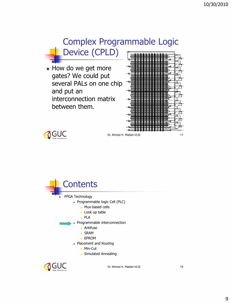
Complex Programmable Logic Device (CPLD)
How do we get more gates? We could put several PALs on one chip and put an interconnection matrix between them.
Dr. Ahmed H. Madian-VLSI 18
Contents FPGA Technology
Programmable logic Cell (PLC)
Mux-based cells
Look up table
PLA
Programmable interconnection
Antifuse
SRAM
EPROM
Placement and Routing
Min-Cut
Simulated Annealing

10/30/2010
10
Dr. Ahmed H. Madian-VLSI 19
Anti fuse
One time programmable
The channel routing uses dedicated rectangular areas of fixed size within the chip called wiring channels
Within the horizontal or vertical channels wires run horizontally or vertically, respectively, within tracks
Actel divides the fixed interconnect wires within each channel into various lengths or wire segments
The designer then programs the interconnections by blowing antifuses and making connections between wire segments
Dr. Ahmed H. Madian-VLSI 20
RC Delay in Antifuse Connections
Elmore Delay (a) A four-antifuse connection. L0 is an output, L1 and L3 are
horizontal tracks, L2 is a long vertical track (LVT), and L4 is an input
(b) An RC-tree model. Each antifuse is modeled by a resistance and each interconnect segment is modeled by a capacitance.
Interconnect delay grows quadratically (xn2) as we increase the interconnect length and the number of antifuses, n

10/30/2010
11
Dr. Ahmed H. Madian-VLSI 21
SRAM Cell
Static Ram reprogrammed according to your bit file, it holds the state until new design is downloaded „1‟ means the switch is on
„0‟ means switch is off
SRAM is reprogrammable, volatile.
Dr. Ahmed H. Madian-VLSI 22
Interconnect delay in FPGA
The vertical lines and horizontal lines run between CLBs.
The general-purpose interconnect joins switch boxes (also known as magic boxes or switching matrices).
The long lines run across the entire chip. It is possible to form internal buses using long lines and the three-state buffers that are next to each CLB.
The direct connections (not used on the XC4000) bypass the switch matrices and directly connect adjacent CLBs.
The Programmable Interconnection Points ( PIP s) are programmable pass transistors that connect the CLB inputs and outputs to the routing network.
The bi-directional ( BIDI ) interconnect buffers restore the logic level and logic strength on long interconnect paths.
10/30/2010
12
Dr. Ahmed H. Madian-VLSI 23
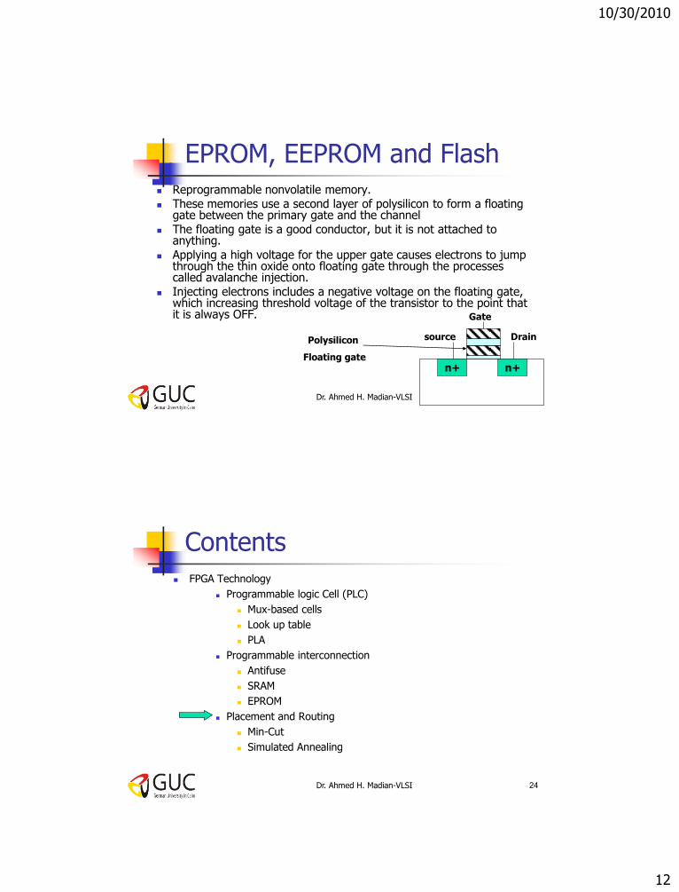
EPROM, EEPROM and Flash Reprogrammable nonvolatile memory. These memories use a second layer of polysilicon to form a floating
gate between the primary gate and the channel The floating gate is a good conductor, but it is not attached to
anything. Applying a high voltage for the upper gate causes electrons to jump
through the thin oxide onto floating gate through the processes called avalanche injection.
Injecting electrons includes a negative voltage on the floating gate, which increasing threshold voltage of the transistor to the point that it is always OFF.
n+n+
source Drain
Gate
Polysilicon
Floating gate
Dr. Ahmed H. Madian-VLSI 24
Contents FPGA Technology
Programmable logic Cell (PLC)
Mux-based cells
Look up table
PLA
Programmable interconnection
Antifuse
SRAM
EPROM
Placement and Routing
Min-Cut
Simulated Annealing

10/30/2010
13
Placement
The process of arranging the circuit components on a layout surface.
Inputs: A set of fixed modules, a netlist.
Goal: Find the best position for each module on the chip according to
appropriate cost functions. Considerations: routability/channel density, wirelength, cut size,
performance, thermal issues, I/O pads.
Dr. Ahmed H. Madian-VLSI 25
Estimation of Wirelength
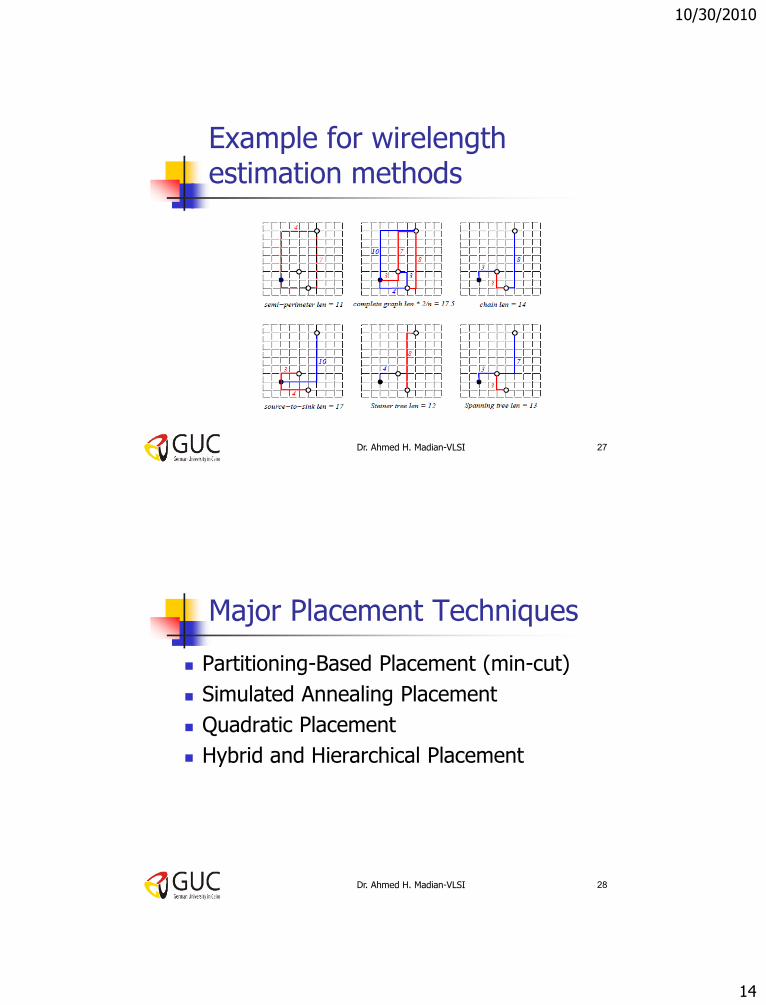
Semi-perimeter method: Half the perimeter of the bounding rectangle that encloses all the pins of the net to be connected. Most widely used approximation!
Complete graph: wire length = (2/n)(i,j) distance (i,j) where I
and j are nodes to be connected and n number of edges.
Minimum chain: Start from one vertex and connect to the closest one, and then to the next closest, etc.
Source-to-sink connection: Connect one pin to all other pins of the net. Not accurate for uncongested chips.
Steiner-tree approximation: Computationally expensive.
Minimum spanning tree
Dr. Ahmed H. Madian-VLSI 26
10/30/2010
14
Example for wirelength estimation methods
Dr. Ahmed H. Madian-VLSI 27
Major Placement Techniques
Partitioning-Based Placement (min-cut)
Simulated Annealing Placement
Quadratic Placement
Hybrid and Hierarchical Placement
Dr. Ahmed H. Madian-VLSI 28
10/30/2010
15
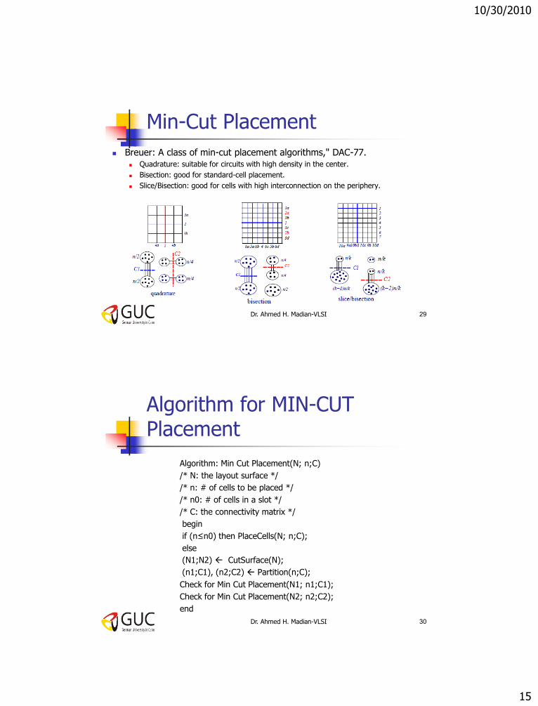
Min-Cut Placement
Breuer: A class of min-cut placement algorithms," DAC-77. Quadrature: suitable for circuits with high density in the center.
Bisection: good for standard-cell placement.
Slice/Bisection: good for cells with high interconnection on the periphery.
Dr. Ahmed H. Madian-VLSI 29
Algorithm for MIN-CUT Placement
Algorithm: Min Cut Placement(N; n;C)
/* N: the layout surface */
/* n: # of cells to be placed */
/* n0: # of cells in a slot */
/* C: the connectivity matrix */
begin
if (n≤n0) then PlaceCells(N; n;C);
else
(N1;N2) CutSurface(N);
(n1;C1), (n2;C2) Partition(n;C);
Check for Min Cut Placement(N1; n1;C1);
Check for Min Cut Placement(N2; n2;C2);
end
Dr. Ahmed H. Madian-VLSI 30

10/30/2010
16
Placement Example
Partition the shown circuit using MIN-CUT Quadrature method
Dr. Ahmed H. Madian-VLSI 31
solution
Dr. Ahmed H. Madian-VLSI 32

10/30/2010
17
Min-Cut Placement with Terminal Propagation
Drawback of the original min-cut placement: Does not consider the positions of terminal pins that enter a region.
What happens if we swap (1, 3, 6, 9) and (2, 4, 5, 7) in the previous example?
Dr. Ahmed H. Madian-VLSI 33
Min-Cut Placement with Terminal Propagation
Dr. Ahmed H. Madian-VLSI 34

10/30/2010
18
MIN- CUT placement
Pros:
Open Cost Function(partitioning cost)
Minimize net cut, edge cut etc.
It is Move Based, Suitable to Timing Driven Placement
Cons:
Lots of “indifferent”moves
May not work well with some cost functions
Multi partitioning
Dr. Ahmed H. Madian-VLSI 35
Simulated Annealing
Sechen and Sangiovanni-Vincentelli, “The TimberWolf placement and routing package," IEEE J. Solid-State Circuits, Feb. 1985;
Stage 1
Modules are moved between different rows as well as within the same row.
Modules overlaps are allowed.
When the temperature is reached below a certain value, stage 2 begins.
Stage 2
Remove overlaps.
Annealing process continues, but only interchanges adjacent modules within the same row.
Dr. Ahmed H. Madian-VLSI 36

10/30/2010
19
Example
Solution Space: All possible arrangements of the modules into rows, possibly with overlaps.
Neighborhood Structure: 3 types of moves M1: Displace a module to a new location.
M2: Interchange two modules.
M3: Change the orientation of a module.
Dr. Ahmed H. Madian-VLSI 37
Dr. Ahmed H. Madian-VLSI 38
Assignment 3 will be available this week on the website
Assignment 3


![An Introduction to VLSI (Very Large Scale Integrated) Circuit Designsburns/EE1001Fall2012/EE1001_2012_HuaTang[1]R… · An Introduction to VLSI (Very Large Scale Integrated) Circuit](https://img.pdfslide.us/doc/110x75/5a9cf78c7f8b9a335c8b6484/an-introduction-to-vlsi-very-large-scale-integrated-circuit-design-sburnsee1001fall2012ee10012012huatang1ran.jpg)