Embed Size (px)
Citation preview
IEEE TRANSACTIONS ON VERY LARGE SCALE INTEGRATION (VLSI) SYSTEMS, VOL. 12, NO. 10, OCTOBER 2004 1015
Power Estimation Techniques for FPGAsJason H. Anderson, Student Member, IEEE, and Farid N. Najm, Fellow, IEEE
Abstract—The dynamic power consumed by a digital CMOS cir-cuit is directly proportional to both switching activity and intercon-nect capacitance. In this paper, we consider early prediction of netactivity and interconnect capacitance in field-programmable gatearray (FPGA) designs. We develop empirical prediction models forthese parameters, suitable for use in power-aware layout synthesis,early power estimation/planning, and other applications. We ex-amine how switching activity on a net changes when delays arezero (zero delay activity) versus when logic delays are considered(logic delay activity) versus when both logic and routing delaysare considered (routed delay activity). We then describe a novelapproach for prelayout activity prediction that estimates a net’srouted delay activity using only zero or logic delay activity values,along with structural and functional circuit properties. For capaci-tance prediction, we show that prediction accuracy is improved byconsidering aspects of the FPGA interconnect architecture in ad-dition to generic parameters, such as net fanout and bounding boxperimeter length. We also demonstrate that there is an inherentvariability (noise) in the switching activity and capacitance of netsthat limits the accuracy attainable in prediction. Experimental re-sults show the proposed prediction models work well given thenoise limitations.
Index Terms—Capacitance, estimation, field-programmablegate arrays (FPGAs), modeling, power, switching activity.
I. INTRODUCTION
FAST time-to-market, steadily decreasing cost, andimproving performance continue to make field-pro-
grammable gate arrays (FPGAs) an attractive technology fordigital circuit implementation. The programmability of FPGAsimplies that more transistors are needed to implement a givenlogic circuit in comparison with custom ASIC technologies.This leads to higher power consumption per logic gate [1]and consequently, FPGA power dissipation is fast becominga “first class” design consideration, along with the traditionalobjectives of circuit performance and area efficiency. In fact,power has been cited as a limiting factor in the ability ofFPGAs to continue to replace ASICs [2]. Today’s largestFPGAs implement complex systems with millions of gates thatcan consume several watts of power [3]. Efficient power-awaredesign for such systems requires estimation tools that gaugepower dissipation early in the design flow. Such tools allowdesign tradeoffs to be considered at a high level of abstraction,reducing design effort and cost.
Several analyses of FPGA power consumption have ap-peared in the literature [1], [3], [4]. These works have shown
Manuscript received September 8, 2003; revised December 31, 2003. Thiswork was supported in part by the Natural Sciences and Engineering ResearchCouncil of Canada.
The authors are with the Department of Electrical and Computer Engi-neering, University of Toronto, Toronto, ON M5S 3G4, Canada (e-mail:[email protected]; [email protected]).
Digital Object Identifier 10.1109/TVLSI.2004.831478
that power dissipation in FPGA devices is predominantly in theprogrammable interconnection network. In the Xilinx Virtex-IIfamily, for example, it was reported that between 50%–70%of total power is dissipated in the interconnection network,with the remainder being dissipated in the clocking, logic, andI/O blocks [3]. The reason for the dominance of interconnectin FPGA power consumption lies in the composition of theinterconnect structures, which consist of prefabricated wiresegments of various lengths, with used and unused routingswitches attached to each wire segment. Wire lengths in FPGAsare generally longer than in ASICs due to the silicon area con-sumed by SRAM configuration cells and other configurationcircuitry.
The majority of power dissipation in today’s FPGAs is dy-namic power dissipation [3], due to the charging and dischargingof parasitic capacitance, as characterized by
(1)
where represents average power consumption, is thecapacitance of a net , is the voltage supply, and is theaverage toggle rate (switching activity) of net . Estimatingpower through (1) requires two parameters for each net: the net’sswitching activity and its capacitance.
We can conceive of several different views of switching ac-tivity, depending on how circuit delays are accounted for. First,activity values can be computed assuming logic and routing de-lays are zero (zero delay activity). Second, activity values canbe computed considering logic delays, but not routing delays(logic delay activity). Third, activity values can be computedconsidering complete logic and routing delays (routed delay ac-tivity). Various approaches to computing switching activity havebeen proposed in the literature, and they can generally be clas-sified as either simulation-based approaches or as probabilisticapproaches [5], [6].
When delays are considered, switching activity normally in-creases due to the introduction of glitches, which are spuriouslogic transitions on a net caused by unequal path delays to thenet’s driving gate. As transitions on gate inputs occur at differenttimes, the net experiences multiple transitions before settling toits final value. The extra activity due to glitching consumes dy-namic power, and previous work has suggested that 20%–70%of total power dissipation in ASICs can be due to glitches [7].
An understanding of how switching activity changes whendelays are considered is important for several reasons. First,since FPGA power dissipation is dominated by interconnect, theconsequences of glitching on total power consumption may bemore severe in FPGAs versus ASICs. In addition, due to the
1063-8210/04$20.00 © 2004 IEEE
1016 IEEE TRANSACTIONS ON VERY LARGE SCALE INTEGRATION (VLSI) SYSTEMS, VOL. 12, NO. 10, OCTOBER 2004
presence of programmable switches in the interconnection net-work, path delays in FPGAs are generally dominated by inter-connect rather than logic delays, suggesting that the severity ofglitching could conceivably be greater in FPGAs than in ASICs.Another reason to study switching activity is that low-powersynthesis techniques may perform optimizations on the basis ofzero delay switching activity data [8], [9], with the assumptionthat such data correlates well with routed delay activity data.It is unknown whether this assumption is valid for FPGA tech-nology.
In addition to switching activity, (1) requires the capacitanceof each net. Early capacitance prediction for FPGAs is not wellstudied and the prefabricated, programmable nature of FPGAinterconnect makes the capacitance prediction problem forFPGAs significantly different from the associated problem inASICs. The dominant role of interconnect in total FPGA powerconsumption implies that characterization and management ofnet capacitance is a crucial part of a power-aware FPGA CADflow.
In this paper, we focus on estimating the power consumedby FPGA interconnect and specifically, we study two separateproblems in FPGA power estimation: 1) switching activity pre-diction and 2) interconnect capacitance prediction. We proposemodels for predicting these parameters prior to routing comple-tion, using the Xilinx Virtex-II PRO commercial FPGA [10] asour investigation vehicle. We envision that the proposed modelscould be applied in variety of scenarios, such as low-power syn-thesis systems, power-aware layout synthesis, and early powerprediction, when accurate routing data is incomplete or unavail-able. The paper is organized as follows. In Section II, we providea background on Virtex-II PRO and give an overview of our pre-diction methodology. Section III considers prelayout switchingactivity prediction. To motivate our work, we study switchingactivity and examine whether zero delay activity values can beused reliably as estimates of routed delay activity. To our knowl-edge, this work represents the first published study of activityin FPGA technology. We then present our activity predictionmodel which estimates the routed delay activity of a net usingthe net’s zero or logic delay activity, as well as functional andstructural properties of a circuit. Section IV deals with intercon-nect capacitance prediction at the placement stage. One of themain results here is that capacitance is not well approximated bygeneric parameters, such as a net’s bounding box half-perimeter.Prediction accuracy is improved significantly when architec-tural aspects of the FPGA interconnect are considered. Anotherimportant contribution of this work is the observation of signifi-cant “noise” in both the capacitance and activity of nets that im-poses limits on the accuracy achievable by any predictor. Con-clusions are offered in Section V. A preliminary version of aportion of this work has appeared in [11] and [12].
II. BACKGROUND
A. Virtex-II PRO FPGA
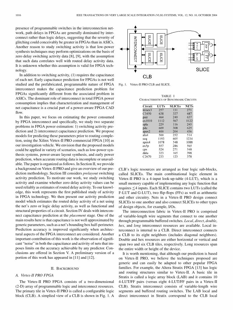
The Virtex-II PRO FPGA consists of a two-dimensional(2-D) array of programmable logic and interconnect resources.The primary tile in Virtex-II PRO is called a configurable logicblock (CLB). A simplied view of a CLB is shown in Fig. 1. A
Fig. 1. Virtex-II PRO CLB and SLICE.
TABLE ICHARACTERISTICS OF BENCHMARK CIRCUITS
CLB’s logic resources are arranged as four logic sub-blocks,called SLICEs. The main combinational logic element inVirtex-II PRO is a 4-input look-up-table (4-LUT), which is asmall memory capable of implementing any logic function thatrequires 4 inputs. Each SLICE contains two LUTs (called theF-LUT and G-LUT), two flip-flops (FFs) as well as arithmeticand other circuitry. Nets in a Virtex-II PRO design connectSLICEs to one another and also connect SLICEs to other typesof design objects, for example, I/Os.
The interconnection fabric in Virtex-II PRO is comprisedof variable-length wire segments that connect to one anotherthrough programmable buffered switches. Local, direct, double,hex, and long interconnect resources are available. Local in-terconnect is internal to a CLB. Direct interconnect connectsa CLB to its eight neighbors (includes diagonal neighbors).Double and hex resources are either horizontal or vertical andspan two and six CLB tiles, respectively. Long resources spanthe entire width or height of the device.
It is worth mentioning, that although our prediction is basedon Virtex-II PRO, we believe the techniques proposed aregeneric and can easily be adapted to other popular FPGAfamilies. For example, the Altera Stratix FPGA [13] has logicand routing structures similar to Virtex-II. A basic tile inStratix is called a logic array block (LAB) and it contains 104-LUT/FF pairs (versus eight 4-LUT/FF pairs in a Virtex-IICLB). Stratix interconnect consists of variable-length wiresegments and buffered routing switches. The LAB local anddirect interconnect in Stratix correspond to the CLB local
ANDERSON AND NAJM: POWER ESTIMATION TECHNIQUES FOR FPGAs 1017
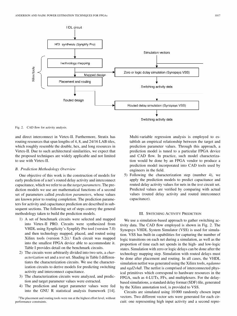
Fig. 2. CAD flow for activity analysis.
and direct interconnect in Virtex-II. Furthermore, Stratix hasrouting resources that span lengths of 4, 8, and 24/16 LAB tiles,which roughly resemble the double, hex, and long resources inVirtex-II. Due to such architectural similarities, we expect thatthe proposed techniques are widely applicable and not limitedto use with Virtex-II.
B. Prediction Methodology Overview
One objective of this work is the construction of models forearly prediction of a net’s routed delay activity and interconnectcapacitance, which we refer to as the target parameters. The pre-diction models we use are mathematical functions of a secondset of parameters called prediction parameters, whose valuesare known prior to routing completion. The prediction parame-ters for activity and capacitance prediction are described in sub-sequent sections. The following set of steps convey the generalmethodology taken to build the prediction models.
1) A set of benchmark circuits were selected and mappedinto Virtex-II PRO. Circuits were synthesized fromVHDL using Synplicity’s Synplify Pro tool (version 7.0)and then technology mapped, placed, and routed usingXilinx tools (version 5.2i).1 Each circuit was mappedinto the smallest FPGA device able to accommodate it.Table I provides detail on the benchmark circuits.
2) The circuits were arbitrarily divided into two sets, a char-acterization set and a test set. Shading in Table I differen-tiates the characterization circuits. We use the character-ization circuits to derive models for predicting switchingactivity and interconnect capacitance.
3) The characterization circuits were analyzed, and predic-tion and target parameter values were extracted.
4) The prediction and target parameter values were fedinto the GNU R statistical analysis framework [14].
1The placement and routing tools were run at the highest effort level, withoutperformance constraints.
Multi-variable regression analysis is employed to es-tablish an empirical relationship between the target andprediction parameter values. Through this approach, aprediction model is tuned to a particular FPGA deviceand CAD flow. In practice, such model characteriza-tion would be done by an FPGA vendor to produce aprediction model incorporated into CAD tools used byengineers in the field.
5) Following the characterization step (number 4), weapply the prediction models to predict capacitance androuted delay activity values for nets in the test circuit set.Predicted values are verified by comparing with actualvalues (routed delay activity and routed interconnectcapacitance).
III. SWITCHING ACTIVITY PREDICTION
We use a simulation-based approach to gather switching ac-tivity data. The CAD flow employed is shown in Fig. 2. TheSynopsys VHDL System Simulator (VSS) is used for simula-tion. VSS has built-in capabilities for capturing the number oflogic transitions on each net during a simulation, as well as theproportion of time each net spends in the high- and low-logicstates. Simulation with zero or logic delays can be done after thetechnology mapping step. Simulation with routed delays mustbe done after placement and routing. In all cases, the VHDLsimulation netlist was generated using the Xilinx tools, ngdannoand ngd2vhdl. The netlist is comprised of interconnected phys-ical primitives which correspond to hardware resources in theFPGA, such as 4-LUTs, FFs, and multiplexers. For the delay-based simulations, a standard delay format (SDF) file, generatedby the Xilinx annotation tool, is provided to VSS.
Circuits are simulated using 10 000 randomly chosen inputvectors. Two different vector sets were generated for each cir-cuit: one representing high input activity and a second repre-
1018 IEEE TRANSACTIONS ON VERY LARGE SCALE INTEGRATION (VLSI) SYSTEMS, VOL. 12, NO. 10, OCTOBER 2004
TABLE IIEFFECT OF GLITCHING ON SWITCHING ACTIVITY
senting low input activity. In the high (low) activity vector set,the probability of an individual input toggling between succes-sive vectors is 50% (25%).
A. Activity Analysis
Using the flow of Fig. 2, we investigated how switching ac-tivity changes when delays are considered. Columns 2–5 ofTable II compare the total number transitions in the logic androuted delay simulations of each circuit with the number of tran-sitions in the zero delay simulation. Columns 2 and 3 (4 and 5)of the table present data for the high (low) activity vector setsimulations. Each table entry represents, for a given circuit, thepercentage increase in the number of transitions in the circuit’slogic or routed delay simulation versus the circuit’s zero delaysimulation. Note that partial glitches were filtered out of thisanalysis and do not register as transitions.2
From Table II, we see that there is a significant increase in ac-tivity when delays are considered. For the high activity vectorset, when logic delays are used, the percentage increase in tran-sition count versus the zero delay simulation ranges from 16%to 60%. When routing delays are used, overall circuit delay in-creases and becomes more variable, leading to more glitchingand higher activity. In the routed delay simulations, the increasein transition count versus the zero delay simulations ranges from28% to 131%. Comparing the data for the two vector sets, weobserve that the increases in activity are somewhat less drasticwhen the low activity vector set is used. Specifically, the activityincreases are about 1/2 to 2/3 of that seen with the high activityvector set. In the low activity vector set, fewer inputs switchsimultaneously between successive vectors, which reduces thepotential for logic transitions on multiple (unequal delay) pathsto a net, leading to reduced glitching.
To investigate whether the increase in activity due to glitchingis distributed uniformly amongst the nets of a circuit, we viewthe zero and logic delay transition count for a net as estimates of
2A partial glitch on a net is a glitch of short duration, shorter than the logicdelay of the net’s driving gate.
the net’s routed delay transition count. We then measure the ab-solute percentage error in the estimates. For example, the errorin a net ’s zero delay activity estimate is
(2)
where and represent the number of transitions onnet in the routed and zero delay simulations, respectively.
Error analysis results (for the high activity vector set) aregiven in columns 6 and 7 of Table II, which shows the averageand standard deviation of error for each circuit. Note that forthis analysis, we ignored the error on nets that transitioned onfewer than 3% of the simulation vectors as we did not considerthe error data for such low activity nets to be statistically signif-icant. In Table II, we see that the mean error in the zero delayactivity values falls in the 26%–60% range. The mean error inlogic delay activity ranges from 14% to 42%. We also observethat coupled with these large mean errors are large error devi-ations, ranging from 14% to 24% for the zero delay case and12%–17% for the logic delay case. This leads us to concludethat zero delay and logic delay activity values do not neces-sarily correlate strongly with routed delay activity values. Al-though not shown here, we also computed error data for the lowactivity vector set simulations. We observed smaller errors forthis vector set, with the mean and deviation of error for each cir-cuit being about 1/2 to 2/3 of that observed for the high activityvector set.
The results in Table II show that activity can change consider-ably when delays are brought into the picture and motivates theneed for early prediction of a net’s routed delay activity. Priorto presenting our prediction approach, we analyze the noise inthe prediction problem.
B. Noise in Switching Activity
In an effort to understand the difficulty of generating accurateprelayout activity estimates, we study the noise in routed delayactivity values by performing an activity analysis on the circuitshown in Fig. 3. The circuit is highly regular from the structural
ANDERSON AND NAJM: POWER ESTIMATION TECHNIQUES FOR FPGAs 1019
Fig. 3. Circuit with regularity.
Fig. 4. Activity change in regular circuit.
and functionality viewpoint and consists of 128 inputs driving128 4-input LUTs, which in turn drive 128 outputs. Each LUTin the circuit is programmed to implement a 4-input logical AND
function.We mapped the circuit in Fig. 3 into Virtex-II PRO and simu-
lated it with both the high and low activity vector sets. We thenexamined the percentage increase in activity on the LUT outputsignals in the routed delay simulation versus the zero delay sim-ulation. Note that the circuit’s regularity implies that variabilityin the activity change on the LUT output signals is largely a re-sult of variable path delays that are known only after layout iscomplete. The results of the analysis are shown in Fig. 4. Thefigure shows the percentage increase in activity on each LUToutput signal for both simulation vector sets (128 data pointsare shown for each vector set—one for each LUT output signal).Observe that despite the circuit’s regularity, the variability in theactivity increase on the LUT output nets is considerable due tothe wide variety of routing resources (and delay paths) in theFPGA routing fabric and the different delays associated with thefour input-to-output paths through a LUT. 3 For the low activityvector set, the activity increase for most nets is in the range of0% to 40%; for the high activity vector set, the increase rangesfrom 0% to 90%.
Real circuits are likely to be much less regular than the circuitof Fig. 3, and we therefore conclude that it will be difficult toachieve a high degree of accuracy in activity prediction at the
3LUT input pins are logically equivalent. The selection of a LUT input pinfor a particular LUT fanin signal is made by the router.
prelayout stage. Nevertheless, in Section III-C, we offer a pre-diction approach which produces activity values that, in com-parison with zero or logic delay activity values, are superior es-timates of routed delay activity.
C. Prediction Model
Before describing our activity prediction approach, we reviewsome terminology related to the graph representation of digitalcircuits. The combinational part of a logic circuit can be repre-sented as a Boolean network, which is a directed acyclic graph(DAG) in which each node represents a single-output logic func-tion and edges between nodes represent input–output dependen-cies between the corresponding logic functions. A primary inputnode is a node with an in-degree of 0; a primary output nodehas an out-degree of 0. Our prediction approach accepts a tech-nology mapped (Virtex-II PRO) FPGA circuit as input. At thislevel of abstraction, internal DAG nodes correspond to the LUTsand other logic elements in the target FPGA device. For a node
in a circuit DAG, let represent the set of nodes thatare fanins of . A node is said to be a predecessor of a node
if there exists a directed path in the circuit DAG from to .The depth of a node , , is the length of the longest path fromany primary input to . In this section, we refer to a node andthe net driven by the node interchangeably; for example, a node
drives net .In FPGA technology, path depth (number of LUTs) is
frequently used as a predictor of path delay at the prelayoutstage [15], [16]. The reason for this is that, unlike in ASICtechnologies such as standard cell, the logic blocks in FPGAsare uniform and have equal drive capability. Furthermore, theprogrammable routing switches in an FPGA’s routing fabricare typically buffered, making connection delay relativelyindependent of fanout. Consequently, without access to moreaccurate delay information extracted from physical layout,depth is viewed as a reasonable estimate of delay. We leveragethis FPGA-specific property in our activity prediction approach,which incorporates delay estimation into a simple model of netglitching severity.
Our approach to activity prediction is analogous to thegenerate and propagate notion that defines how carry signalvalues are assigned in arithmetic circuits. In such circuits,the carry value for a particular bit may either be generatedby the bit, or it may be propagated from a lower-order bit.For activity prediction, consider a node with logic function
. Similar to carry signal operation,glitches on ’s output may come from two sources: they may
1020 IEEE TRANSACTIONS ON VERY LARGE SCALE INTEGRATION (VLSI) SYSTEMS, VOL. 12, NO. 10, OCTOBER 2004
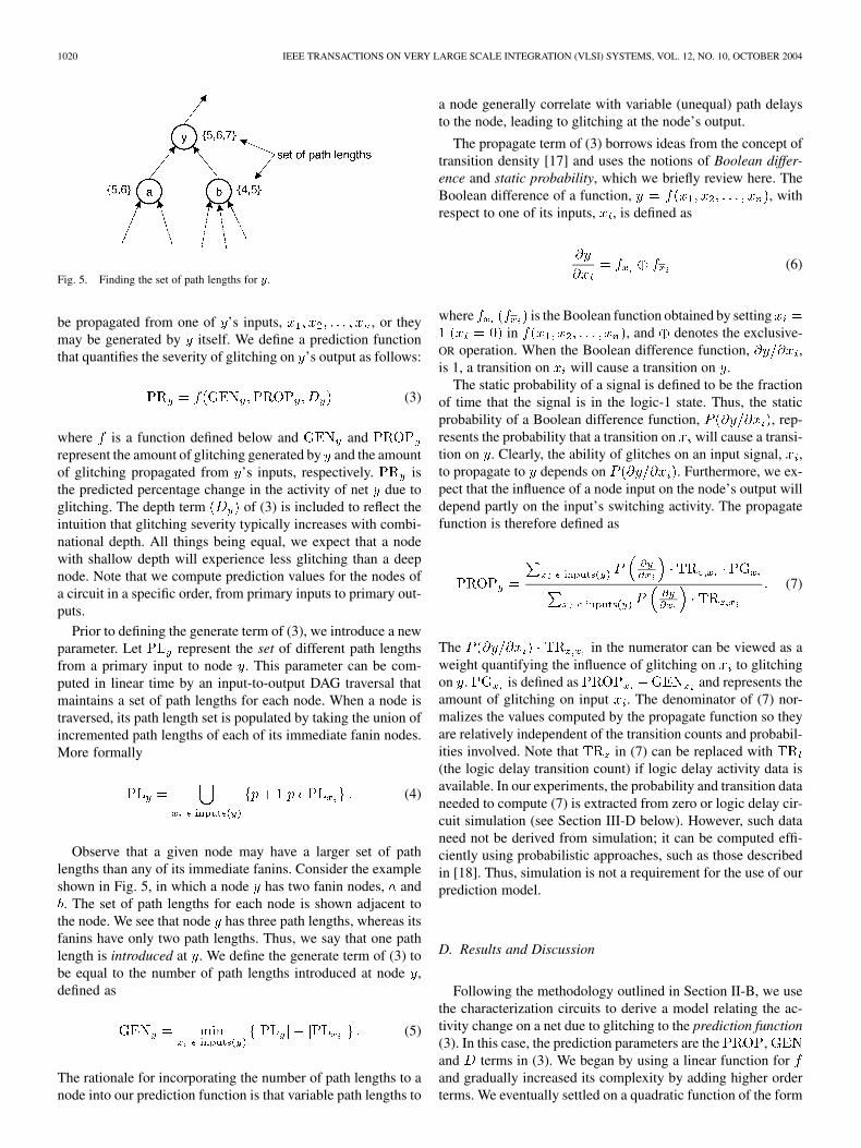
Fig. 5. Finding the set of path lengths for y.
be propagated from one of ’s inputs, , or theymay be generated by itself. We define a prediction functionthat quantifies the severity of glitching on ’s output as follows:
(3)
where is a function defined below and andrepresent the amount of glitching generated by and the amountof glitching propagated from ’s inputs, respectively. isthe predicted percentage change in the activity of net due toglitching. The depth term of (3) is included to reflect theintuition that glitching severity typically increases with combi-national depth. All things being equal, we expect that a nodewith shallow depth will experience less glitching than a deepnode. Note that we compute prediction values for the nodes ofa circuit in a specific order, from primary inputs to primary out-puts.
Prior to defining the generate term of (3), we introduce a newparameter. Let represent the set of different path lengthsfrom a primary input to node . This parameter can be com-puted in linear time by an input-to-output DAG traversal thatmaintains a set of path lengths for each node. When a node istraversed, its path length set is populated by taking the union ofincremented path lengths of each of its immediate fanin nodes.More formally
(4)
Observe that a given node may have a larger set of pathlengths than any of its immediate fanins. Consider the exampleshown in Fig. 5, in which a node has two fanin nodes, and. The set of path lengths for each node is shown adjacent to
the node. We see that node has three path lengths, whereas itsfanins have only two path lengths. Thus, we say that one pathlength is introduced at . We define the generate term of (3) tobe equal to the number of path lengths introduced at node ,defined as
(5)
The rationale for incorporating the number of path lengths to anode into our prediction function is that variable path lengths to
a node generally correlate with variable (unequal) path delaysto the node, leading to glitching at the node’s output.
The propagate term of (3) borrows ideas from the concept oftransition density [17] and uses the notions of Boolean differ-ence and static probability, which we briefly review here. TheBoolean difference of a function, , withrespect to one of its inputs, , is defined as
(6)
where is the Boolean function obtained by settingin , and denotes the exclusive-
OR operation. When the Boolean difference function, ,is 1, a transition on will cause a transition on .
The static probability of a signal is defined to be the fractionof time that the signal is in the logic-1 state. Thus, the staticprobability of a Boolean difference function, , rep-resents the probability that a transition on will cause a transi-tion on . Clearly, the ability of glitches on an input signal, ,to propagate to depends on . Furthermore, we ex-pect that the influence of a node input on the node’s output willdepend partly on the input’s switching activity. The propagatefunction is therefore defined as
(7)
The in the numerator can be viewed as aweight quantifying the influence of glitching on to glitchingon . is defined as and represents theamount of glitching on input . The denominator of (7) nor-malizes the values computed by the propagate function so theyare relatively independent of the transition counts and probabil-ities involved. Note that in (7) can be replaced with(the logic delay transition count) if logic delay activity data isavailable. In our experiments, the probability and transition dataneeded to compute (7) is extracted from zero or logic delay cir-cuit simulation (see Section III-D below). However, such dataneed not be derived from simulation; it can be computed effi-ciently using probabilistic approaches, such as those describedin [18]. Thus, simulation is not a requirement for the use of ourprediction model.
D. Results and Discussion
Following the methodology outlined in Section II-B, we usethe characterization circuits to derive a model relating the ac-tivity change on a net due to glitching to the prediction function(3). In this case, the prediction parameters are the ,and terms in (3). We began by using a linear function forand gradually increased its complexity by adding higher orderterms. We eventually settled on a quadratic function of the form
ANDERSON AND NAJM: POWER ESTIMATION TECHNIQUES FOR FPGAs 1021
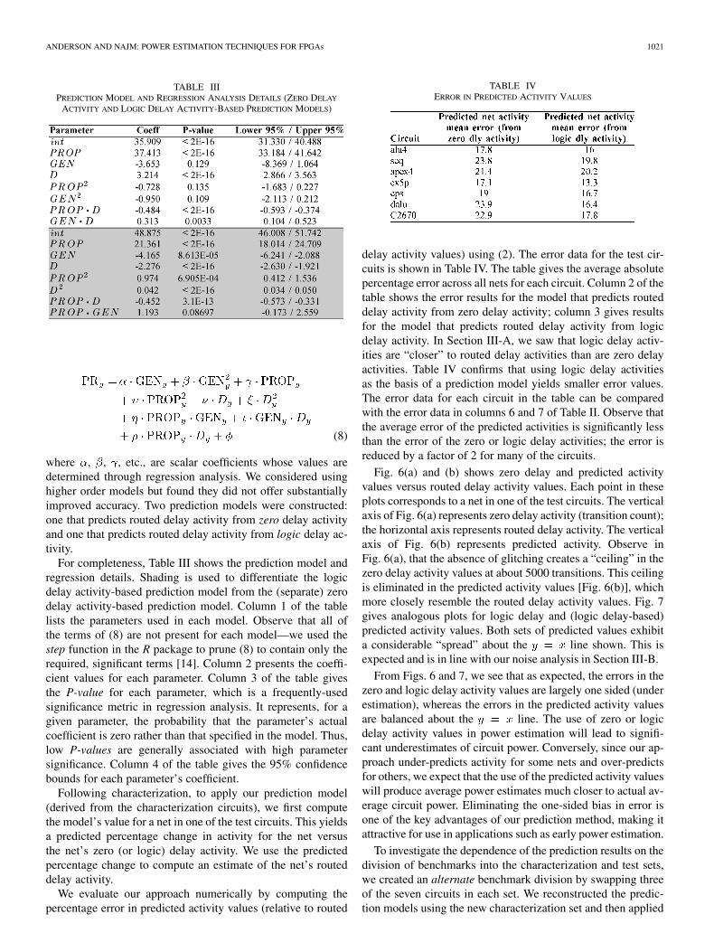
TABLE IIIPREDICTION MODEL AND REGRESSION ANALYSIS DETAILS (ZERO DELAY
ACTIVITY AND LOGIC DELAY ACTIVITY-BASED PREDICTION MODELS)
(8)
where , , , etc., are scalar coefficients whose values aredetermined through regression analysis. We considered usinghigher order models but found they did not offer substantiallyimproved accuracy. Two prediction models were constructed:one that predicts routed delay activity from zero delay activityand one that predicts routed delay activity from logic delay ac-tivity.
For completeness, Table III shows the prediction model andregression details. Shading is used to differentiate the logicdelay activity-based prediction model from the (separate) zerodelay activity-based prediction model. Column 1 of the tablelists the parameters used in each model. Observe that all ofthe terms of (8) are not present for each model—we used thestep function in the R package to prune (8) to contain only therequired, significant terms [14]. Column 2 presents the coeffi-cient values for each parameter. Column 3 of the table givesthe P-value for each parameter, which is a frequently-usedsignificance metric in regression analysis. It represents, for agiven parameter, the probability that the parameter’s actualcoefficient is zero rather than that specified in the model. Thus,low P-values are generally associated with high parametersignificance. Column 4 of the table gives the 95% confidencebounds for each parameter’s coefficient.
Following characterization, to apply our prediction model(derived from the characterization circuits), we first computethe model’s value for a net in one of the test circuits. This yieldsa predicted percentage change in activity for the net versusthe net’s zero (or logic) delay activity. We use the predictedpercentage change to compute an estimate of the net’s routeddelay activity.
We evaluate our approach numerically by computing thepercentage error in predicted activity values (relative to routed
TABLE IVERROR IN PREDICTED ACTIVITY VALUES
delay activity values) using (2). The error data for the test cir-cuits is shown in Table IV. The table gives the average absolutepercentage error across all nets for each circuit. Column 2 of thetable shows the error results for the model that predicts routeddelay activity from zero delay activity; column 3 gives resultsfor the model that predicts routed delay activity from logicdelay activity. In Section III-A, we saw that logic delay activ-ities are “closer” to routed delay activities than are zero delayactivities. Table IV confirms that using logic delay activitiesas the basis of a prediction model yields smaller error values.The error data for each circuit in the table can be comparedwith the error data in columns 6 and 7 of Table II. Observe thatthe average error of the predicted activities is significantly lessthan the error of the zero or logic delay activities; the error isreduced by a factor of 2 for many of the circuits.
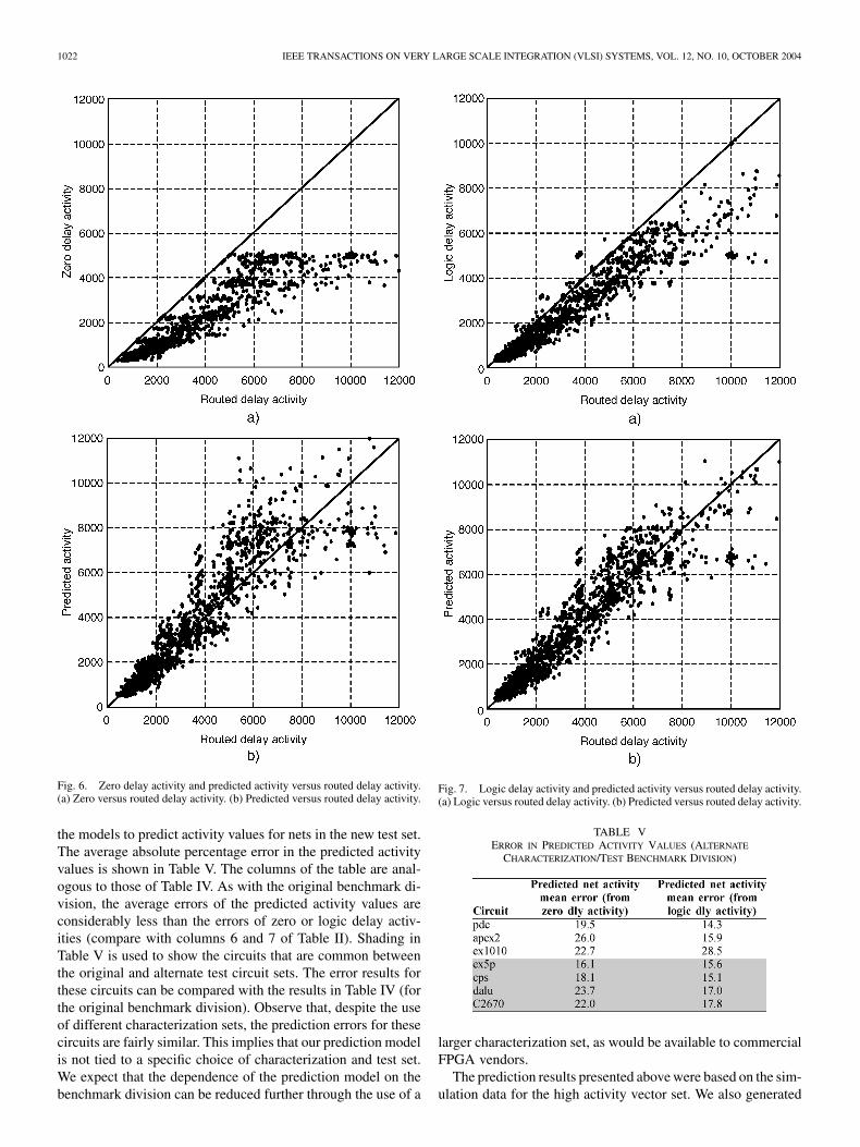
Fig. 6(a) and (b) shows zero delay and predicted activityvalues versus routed delay activity values. Each point in theseplots corresponds to a net in one of the test circuits. The verticalaxis of Fig. 6(a) represents zero delay activity (transition count);the horizontal axis represents routed delay activity. The verticalaxis of Fig. 6(b) represents predicted activity. Observe inFig. 6(a), that the absence of glitching creates a “ceiling” in thezero delay activity values at about 5000 transitions. This ceilingis eliminated in the predicted activity values [Fig. 6(b)], whichmore closely resemble the routed delay activity values. Fig. 7gives analogous plots for logic delay and (logic delay-based)predicted activity values. Both sets of predicted values exhibita considerable “spread” about the line shown. This isexpected and is in line with our noise analysis in Section III-B.
From Figs. 6 and 7, we see that as expected, the errors in thezero and logic delay activity values are largely one sided (underestimation), whereas the errors in the predicted activity valuesare balanced about the line. The use of zero or logicdelay activity values in power estimation will lead to signifi-cant underestimates of circuit power. Conversely, since our ap-proach under-predicts activity for some nets and over-predictsfor others, we expect that the use of the predicted activity valueswill produce average power estimates much closer to actual av-erage circuit power. Eliminating the one-sided bias in error isone of the key advantages of our prediction method, making itattractive for use in applications such as early power estimation.
To investigate the dependence of the prediction results on thedivision of benchmarks into the characterization and test sets,we created an alternate benchmark division by swapping threeof the seven circuits in each set. We reconstructed the predic-tion models using the new characterization set and then applied
1022 IEEE TRANSACTIONS ON VERY LARGE SCALE INTEGRATION (VLSI) SYSTEMS, VOL. 12, NO. 10, OCTOBER 2004
Fig. 6. Zero delay activity and predicted activity versus routed delay activity.(a) Zero versus routed delay activity. (b) Predicted versus routed delay activity.
the models to predict activity values for nets in the new test set.The average absolute percentage error in the predicted activityvalues is shown in Table V. The columns of the table are anal-ogous to those of Table IV. As with the original benchmark di-vision, the average errors of the predicted activity values areconsiderably less than the errors of zero or logic delay activ-ities (compare with columns 6 and 7 of Table II). Shading inTable V is used to show the circuits that are common betweenthe original and alternate test circuit sets. The error results forthese circuits can be compared with the results in Table IV (forthe original benchmark division). Observe that, despite the useof different characterization sets, the prediction errors for thesecircuits are fairly similar. This implies that our prediction modelis not tied to a specific choice of characterization and test set.We expect that the dependence of the prediction model on thebenchmark division can be reduced further through the use of a
Fig. 7. Logic delay activity and predicted activity versus routed delay activity.(a) Logic versus routed delay activity. (b) Predicted versus routed delay activity.
TABLE VERROR IN PREDICTED ACTIVITY VALUES (ALTERNATE
CHARACTERIZATION/TEST BENCHMARK DIVISION)
larger characterization set, as would be available to commercialFPGA vendors.
The prediction results presented above were based on the sim-ulation data for the high activity vector set. We also generated
ANDERSON AND NAJM: POWER ESTIMATION TECHNIQUES FOR FPGAs 1023
prediction models for the low activity vector set data and foundsimilar results, though there is less severe glitching associatedwith lower input activity. Thus, we expect that our predictionmethod can be applied effectively for a range of input switchingactivities. A direction for future work is to augment the predic-tion approach to automatically account for various amounts ofprimary input switching activity.
IV. INTERCONNECT CAPACITANCE PREDICTION
We now move on to interconnect capacitance prediction at theplacement stage. We begin with a brief review of related work.
A. Related Work
Several works have considered capacitance estimation in thecontext of power-aware FPGA CAD tools. At the technologymapping level (prelayout), net capacitance has been estimatedusing a linear function of fanout [8], [9]. Previous placement-based capacitance estimates have appeared in [19] and [20]. Atthis level, the approach taken has been to use a combination ofa net’s bounding box half-perimeter and its fanout to estimateits routed capacitance. These prior works use generic, non-ar-chitecture-specific parameters to predict capacitance.
A problem related to capacitance estimation is that of FPGAdelay estimation, which is well studied in the literature. Theproblems differ from each other in that delay estimates areneeded for individual driver/load connections whereas capac-itance estimates are needed for entire (multi-fanout) nets. In[21], a delay estimation model is constructed during placementby executing a pre-routing step in which “dummy” routeshaving known and distances are made. Following this, atable that relates delay to distance is constructed; table valuesare used as delay estimates during placement. The delay esti-mation model development approach used in [22] and [23] issimilar to our own. Routed designs are analyzed and connectiondelays are correlated with placement parameters, producing anempirically-derived estimation model. In [24], characteristicsof a target FPGA’s interconnect architecture are used to predictdelay within a partitioning-based placement system. In thiscase, the FPGA interconnect is hierarchical and the placer’spartitioning levels are chosen to match the underlying FPGAinterconnect hierarchy. As such, the placer has knowledge ofthe interconnect resources likely to be used in the routing of netsthat are cut (and uncut) at a given partitioning level. Like [24],our capacitance estimator also considers architecture-specificcriteria to improve estimation accuracy.
B. Noise in Interconnect Capacitance
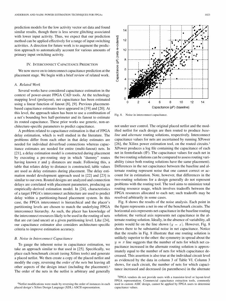
To gauge the inherent noise in capacitance estimation, wetake an approach similar to that used in [25]. Specifically, weplace each benchmark circuit (using Xilinx tools) and generatea placed netlist. We then create a copy of the placed netlist andmodify the copy, reversing the order of the nets but leaving allother aspects of the design intact (including the placement).4
The order of the nets in the netlist is arbitrary and generally
4Netlist modifications were made by reversing the order of instances in eachplaced design’s Xilinx Design Language (XDL) ASCII representation.
Fig. 8. Noise in interconnect capacitance.
not under user control. The original placed netlist and the mod-ified netlist for each design are then routed to produce base-line and alternate routing solutions, respectively. Interconnectcapacitance values for nets are ascertained by running XPower[26], the Xilinx power estimation tool, on the routed circuits.5
XPower produces a log file containing the capacitance of eachnet in femtofarads (fF). The capacitance values for each net inthe two routing solutions can be compared to assess routing vari-ability (since both routing solutions have the same placement).Differences in the net capacitance between the baseline and al-ternate routing represent noise that one cannot correct or ac-count for in estimation. Note, however, that differences in thetwo-routing solutions for a design generally do not representproblems with the routing tool. The tool aims to minimize totalrouting resource usage, which involves tradeoffs between theFPGA resources allocated to each net; such tradeoffs may beresolved arbitrarily in some cases.
Fig. 8 shows the results of the noise analysis. Each point inthe figure represents a net in one of the benchmark circuits. Thehorizontal axis represents net capacitance in the baseline routingsolution; the vertical axis represents net capacitance in the al-ternate routing solution. Ideally, in the absence of variability, allpoints would lie on the line shown . However, Fig. 8shows there to be substantial noise in net capacitance. Noticethat the results in Fig. 8 illustrate that one routing solution isunlikely superior to the other: the symmetry in spread about the
line suggests that the number of nets for which net ca-pacitance increased in the alternate routing solution is approx-imately equal to the number of nets for which capacitance de-creased. This assertion is also true at the individual circuit levelas evidenced by the data in column 3 of Table VI. Column 3shows, for each circuit, the number of nets for which capaci-tance increased and decreased (in parentheses) in the alternate
5FPGA vendors do not provide users with a transistor-level or layout-levelFPGA representation. Commercial capacitance extraction tools, commonlyused in custom ASIC design, cannot be applied by FPGA users to determinecapacitance values.
1024 IEEE TRANSACTIONS ON VERY LARGE SCALE INTEGRATION (VLSI) SYSTEMS, VOL. 12, NO. 10, OCTOBER 2004
TABLE VINOISE IN INDIVIDUAL CIRCUITS
routing solution versus baseline. The number of increases anddecreases are roughly equal for each circuit.
We computed the absolute value of the percentage change incapacitance for each net in the alternate routing versus the base-line. Column 2 of Table VI shows the average absolute changefor each circuit. The average change across all circuits is 22%.This represents a statistical lower bound on the error in capac-itance estimation; estimation accuracy cannot be improved be-yond this noise floor error limit.
C. Prediction Model
Having analyzed the noise in capacitance, we now presentour prediction model. In comparison with prediction at theprelayout stage, a larger number of prediction parameters areavailable for prediction at the placement stage (e.g., physicaldesign data). Consequently, we take a slightly different ap-proach to capacitance prediction as compared with that takenfor activity prediction. We first define the prediction param-eters used in our model and following this, we explain therationale of why the chosen parameters may correlate with netinterconnect capacitance. Section IV-D presents experimentalresults showing which of the parameters are best for use in acapacitance prediction model.
CAD applications such as power-aware placement and earlypower planning require that capacitance estimates be producedquickly as they are typically needed within the inner loop of de-sign optimization. Consequently, we focus on parameters withlow computational requirements. Considering a net , the fol-lowing are known at the placement stage:
fanout of net ;half-perimeter of net ’s bounding box, asmeasured in CLB tiles;span of net in the - and -dimensions, re-spectively;number of CLB (or I/O) tiles in which nethas at least 1 pin;defined as and , re-spectively;number of load pins on net that are F-LUTand G-LUT inputs, respectively;average estimated routing congestion in net
’s bounding box.
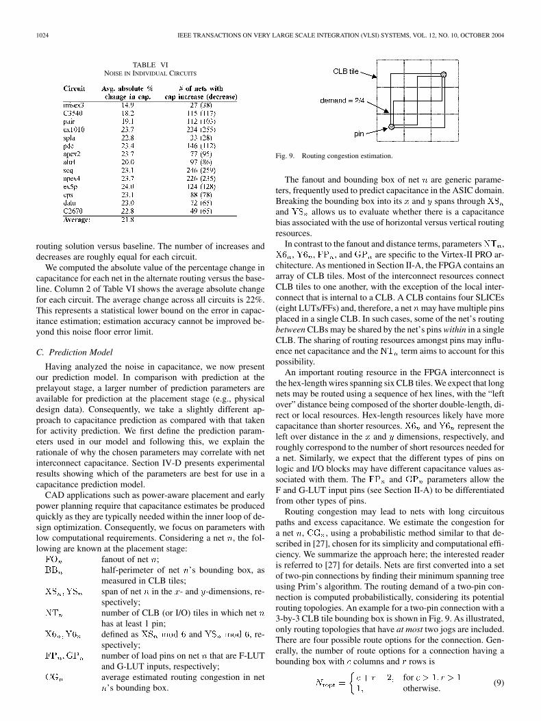
Fig. 9. Routing congestion estimation.
The fanout and bounding box of net are generic parame-ters, frequently used to predict capacitance in the ASIC domain.Breaking the bounding box into its and spans throughand allows us to evaluate whether there is a capacitancebias associated with the use of horizontal versus vertical routingresources.
In contrast to the fanout and distance terms, parameters ,, , , and are specific to the Virtex-II PRO ar-
chitecture. As mentioned in Section II-A, the FPGA contains anarray of CLB tiles. Most of the interconnect resources connectCLB tiles to one another, with the exception of the local inter-connect that is internal to a CLB. A CLB contains four SLICEs(eight LUTs/FFs) and, therefore, a net may have multiple pinsplaced in a single CLB. In such cases, some of the net’s routingbetween CLBs may be shared by the net’s pins within in a singleCLB. The sharing of routing resources amongst pins may influ-ence net capacitance and the term aims to account for thispossibility.
An important routing resource in the FPGA interconnect isthe hex-length wires spanning six CLB tiles. We expect that longnets may be routed using a sequence of hex lines, with the “leftover” distance being composed of the shorter double-length, di-rect or local resources. Hex-length resources likely have morecapacitance than shorter resources. and represent theleft over distance in the and dimensions, respectively, androughly correspond to the number of short resources needed fora net. Similarly, we expect that the different types of pins onlogic and I/O blocks may have different capacitance values as-sociated with them. The and parameters allow theF and G-LUT input pins (see Section II-A) to be differentiatedfrom other types of pins.
Routing congestion may lead to nets with long circuitouspaths and excess capacitance. We estimate the congestion fora net , , using a probabilistic method similar to that de-scribed in [27], chosen for its simplicity and computational effi-ciency. We summarize the approach here; the interested readeris referred to [27] for details. Nets are first converted into a setof two-pin connections by finding their minimum spanning treeusing Prim’s algorithm. The routing demand of a two-pin con-nection is computed probabilistically, considering its potentialrouting topologies. An example for a two-pin connection with a3-by-3 CLB tile bounding box is shown in Fig. 9. As illustrated,only routing topologies that have at most two jogs are included.There are four possible route options for the connection. Gen-erally, the number of route options for a connection having abounding box with columns and rows is
forotherwise.
(9)
ANDERSON AND NAJM: POWER ESTIMATION TECHNIQUES FOR FPGAs 1025
Similarly, the number of a connection’s route options that crossa specific CLB tile edge can also be expressed analytically (de-tails are omitted here due to limited space). Dividing the numberof a connection’s route options that cross a specific CLB tileedge by the total number of route options for the connectionyields the probability that the connection’s route will traversethe CLB tile edge. This probability can be viewed as the demandexerted by the connection on a tile edge (see Fig. 9). The routingdemands contributed by each two-pin connection in each netare tallied to produce a total routing demand on each CLB tile.The term represents the average routing demand across allCLB tile edges within net ’s bounding box.
The capacitance of nets in the characterization circuit set werefit to a mathematical function of the parameters as described.The result is a mathematical model that may be applied to pre-dict capacitance values of nets in the test circuit set. We de-veloped separate estimation models for high-fanout nets ( 10loads) and low-fanout nets ( 10 loads) and apply each modelaccordingly in our experimental study (Section III-D). We eval-uate a range of models and use the labels , , andto represent linear, quadratic, and cubic functions, respectively.Models are specified using a function type, followed by a param-eter list in parentheses. Using this terminology, a model speci-fied as would predict the capacitance of a net ,
, using a linear function of the net’s fanout and its boundingbox half-perimeter
(10)
where , , and are scalar coefficients with values determinedthrough regression analysis. Note that cross-variable terms (e.g.,
) are omitted, unless explicitly included in the pa-rameter list.
D. Results and Discussion
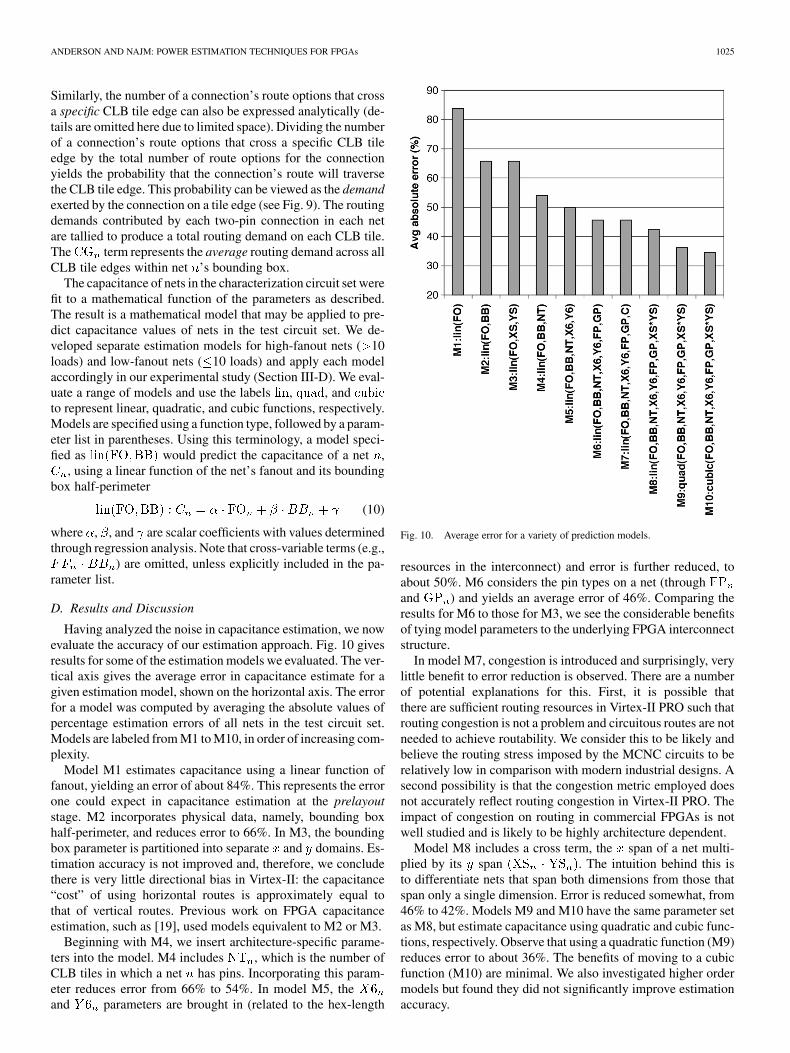
Having analyzed the noise in capacitance estimation, we nowevaluate the accuracy of our estimation approach. Fig. 10 givesresults for some of the estimation models we evaluated. The ver-tical axis gives the average error in capacitance estimate for agiven estimation model, shown on the horizontal axis. The errorfor a model was computed by averaging the absolute values ofpercentage estimation errors of all nets in the test circuit set.Models are labeled from M1 to M10, in order of increasing com-plexity.
Model M1 estimates capacitance using a linear function offanout, yielding an error of about 84%. This represents the errorone could expect in capacitance estimation at the prelayoutstage. M2 incorporates physical data, namely, bounding boxhalf-perimeter, and reduces error to 66%. In M3, the boundingbox parameter is partitioned into separate and domains. Es-timation accuracy is not improved and, therefore, we concludethere is very little directional bias in Virtex-II: the capacitance“cost” of using horizontal routes is approximately equal tothat of vertical routes. Previous work on FPGA capacitanceestimation, such as [19], used models equivalent to M2 or M3.
Beginning with M4, we insert architecture-specific parame-ters into the model. M4 includes , which is the number ofCLB tiles in which a net has pins. Incorporating this param-eter reduces error from 66% to 54%. In model M5, theand parameters are brought in (related to the hex-length
Fig. 10. Average error for a variety of prediction models.
resources in the interconnect) and error is further reduced, toabout 50%. M6 considers the pin types on a net (throughand ) and yields an average error of 46%. Comparing theresults for M6 to those for M3, we see the considerable benefitsof tying model parameters to the underlying FPGA interconnectstructure.
In model M7, congestion is introduced and surprisingly, verylittle benefit to error reduction is observed. There are a numberof potential explanations for this. First, it is possible thatthere are sufficient routing resources in Virtex-II PRO such thatrouting congestion is not a problem and circuitous routes are notneeded to achieve routability. We consider this to be likely andbelieve the routing stress imposed by the MCNC circuits to berelatively low in comparison with modern industrial designs. Asecond possibility is that the congestion metric employed doesnot accurately reflect routing congestion in Virtex-II PRO. Theimpact of congestion on routing in commercial FPGAs is notwell studied and is likely to be highly architecture dependent.
Model M8 includes a cross term, the span of a net multi-plied by its span . The intuition behind this isto differentiate nets that span both dimensions from those thatspan only a single dimension. Error is reduced somewhat, from46% to 42%. Models M9 and M10 have the same parameter setas M8, but estimate capacitance using quadratic and cubic func-tions, respectively. Observe that using a quadratic function (M9)reduces error to about 36%. The benefits of moving to a cubicfunction (M10) are minimal. We also investigated higher ordermodels but found they did not significantly improve estimationaccuracy.
1026 IEEE TRANSACTIONS ON VERY LARGE SCALE INTEGRATION (VLSI) SYSTEMS, VOL. 12, NO. 10, OCTOBER 2004
TABLE VIIPREDICTION MODEL AND REGRESSION ANALYSIS DETAILS (LOW-FANOUT
AND HIGH-FANOUT PREDICTION MODELS)
The parameter coefficients for M10 and other regression anal-ysis data are provided in Table VII. The unshaded portion of thetable shows the low-fanout net prediction model ( 10 loads);the shaded portion of the table corresponds to the predictionmodel used for high-fanout nets. About 5% of the nets in thecircuits are high-fanout. The columns of the table are analogousto those of Table III. Observe that a very simple model sufficesfor predicting the capacitance of high-fanout nets. Only the net’sfanout, bounding box, the number of CLB tiles, and pin typesare included. Further, the P-value for the bounding box termimplies a fairly weak significance. We experimented with drop-ping this term and observed only a small decrease in predic-tion accuracy ( 1%). We found that the use of more complexmodels for the high-fanout nets resulted in “overfitting” to thecharacterization circuits that led to lower prediction accuracy inthe test circuits. This is likely due to a greater noise presencein high-fanout versus low-fanout nets. The overfitting phenom-enon was not observed for the low-fanout net modeling: betterfitting during characterization for such nets resulted in betterprediction accuracy.
Model M10 yields average error values of about 35%. Errorresults for the individual test circuits are shown in column 2 ofTable VIII. From Table VI, we see that the noise floor errorsfor these circuits fall in the 20%–24% range. The differencebetween the prediction and noise floor errors limits the poten-tial for improvement in prediction accuracy. Given the range ofrouting resource types available in the FPGA, we consider theprediction accuracy to be quite good.
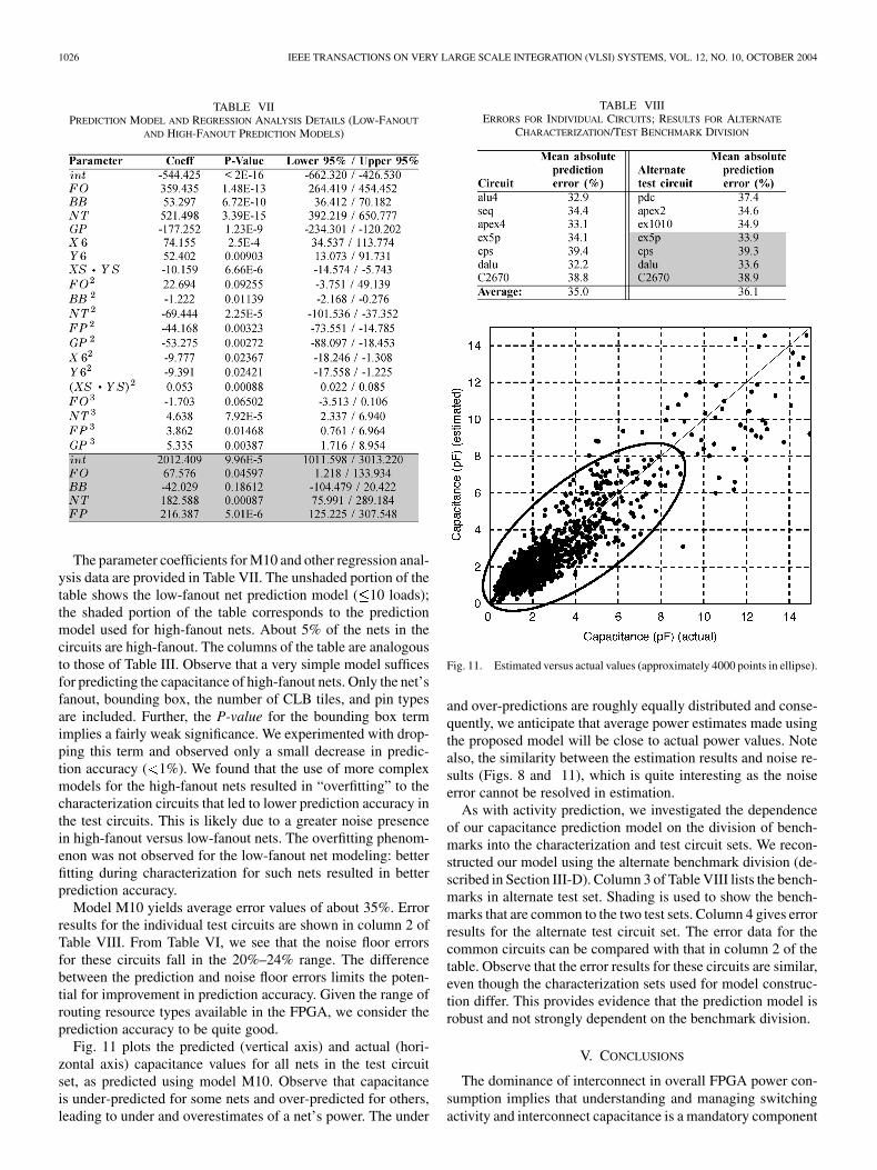
Fig. 11 plots the predicted (vertical axis) and actual (hori-zontal axis) capacitance values for all nets in the test circuitset, as predicted using model M10. Observe that capacitanceis under-predicted for some nets and over-predicted for others,leading to under and overestimates of a net’s power. The under
TABLE VIIIERRORS FOR INDIVIDUAL CIRCUITS; RESULTS FOR ALTERNATE
CHARACTERIZATION/TEST BENCHMARK DIVISION
Fig. 11. Estimated versus actual values (approximately 4000 points in ellipse).
and over-predictions are roughly equally distributed and conse-quently, we anticipate that average power estimates made usingthe proposed model will be close to actual power values. Notealso, the similarity between the estimation results and noise re-sults (Figs. 8 and 11), which is quite interesting as the noiseerror cannot be resolved in estimation.
As with activity prediction, we investigated the dependenceof our capacitance prediction model on the division of bench-marks into the characterization and test circuit sets. We recon-structed our model using the alternate benchmark division (de-scribed in Section III-D). Column 3 of Table VIII lists the bench-marks in alternate test set. Shading is used to show the bench-marks that are common to the two test sets. Column 4 gives errorresults for the alternate test circuit set. The error data for thecommon circuits can be compared with that in column 2 of thetable. Observe that the error results for these circuits are similar,even though the characterization sets used for model construc-tion differ. This provides evidence that the prediction model isrobust and not strongly dependent on the benchmark division.
V. CONCLUSIONS
The dominance of interconnect in overall FPGA power con-sumption implies that understanding and managing switchingactivity and interconnect capacitance is a mandatory component
ANDERSON AND NAJM: POWER ESTIMATION TECHNIQUES FOR FPGAs 1027
of power-aware FPGA computer-aided design. In this paper,we studied activity and capacitance prediction for FPGAs andproposed models for the early prediction of these parameters.Our activity prediction approach estimates routed delay activityvalues for a net using zero or logic delay activity values aswell as circuit functional and structural properties. The proposedcapacitance prediction model uses generic parameters such asfanout and bounding box length as well as parameters that arespecific to the underlying FPGA routing fabric. We conducted anoise analysis of activity and capacitance and established limitson the potential accuracy achievable in prediction. The predic-tion models work well given the noise limitations and we expectthat they will be useful in applications such as low-power syn-thesis, early-power estimation, and power-aware layout.
REFERENCES
[1] V. George and J. Rabaey, Low-Energy FPGAs: Architecture and De-sign. Norwell, MA: Kluwer, 2001.
[2] L. Stok and J. Cohn, “There is life left in ASICs,” in Proc. IEEE Int.Symp. Physical Design, 2003, pp. 48–50.
[3] L. Shang, A. Kaviani, and K. Bathala, “Dynamic power consumptionin the Virtex-II FPGA family,” in Proc. ACM Int. Symp. Field-Pro-grammable Gate-Arrays, 2002, pp. 157–164.
[4] K. Poon, A. Yan, and S. Wilton, “A flexible power model for FPGAs,”in Proc. Int. Conf. Field-Programmable Logic and Applications, 2002,pp. 312–321.
[5] F. Najm, “A survey of power estimation techniques in VLSI circuits,”IEEE Trans. VLSI Syst., vol. 2, pp. 446–455, Dec. 1994.
[6] H. Soeleman, K. Roy, and T.-L. Chou, “Estimating circuit activity incombinational CMOS digital circuits,” IEEE Des. Test Comput., pp.112–119, Apr.–June 2000.
[7] A. Shen, A. Ghosh, S. Devadas, and K. Keutzer, “On average powerdissipation and random pattern testability of CMOS combinational logicnetworks,” in Proc. IEEE Int. Conf. Computer-Aided Design, 1992, pp.402–407.
[8] H. Li, W.-K. Mak, and S. Katkoori, “LUT-based FPGA technology map-ping for power minimization with optimal depth,” in Proc. IEEE Com-puter Society Workshop VLSI, 2001, pp. 123–128.
[9] A. Farrahi and M. Sarrafzadeh, “FPGA technology mapping for powerminimization,” in Proc. Int. Workshop Field-Programmable Logic andApplications, 1994, pp. 167–174.
[10] Virtex II PRO FPGA Data Sheet, Xilinx Inc., San Jose, CA, 2003.[11] J. Anderson and F. Najm, “Switching activity analysis and pre-layout
activity prediction for FPGAs,” in Proc. IEEE Int. Workshop System-Level Interconnect Prediction, 2003, pp. 15–21.
[12] , “Interconnect capacitance estimation for FPGAs,” in Proc. IEEEAsia South Pacific Design Automation Conf., Yokohama, Japan, 2004,pp. 713–718.
[13] Stratix FPGA Device Handbook, Altera Corp., San Jose, CA, 2003.[14] (2003) The R Project for Statistical Computing. [Online] Available:
http://www.r-project.org[15] J. Cong and Y. Ding, “Flowmap: an optimal technology mapping al-
gorithm for delay optimization in look-up-table based FPGA designs,”IEEE Trans. Computer-Aided Design, vol. 13, pp. 1–12, Jan. 1994.
[16] R. Francis, J. Rose, and Z. Vranesic, “Technology mapping for lookuptable-based FPGAs for performance,” in Proc. IEEE Int. Conf. Com-puter-Aided Design, 1991, pp. 568–571.
[17] F. Najm, “Transition density: a new measure of activity in digital cir-cuits,” IEEE Trans. Computer-Aided Design, vol. 12, pp. 310–323, Feb.1993.
[18] G. Yeap, Practical Low Power Digital VLSI Design. Norwell, MA:Kluwer, 1998.
[19] K. Roy, “Power-dissipation driven FPGA place and route under timingconstraints,” IEEE Trans. Circuits Syst., vol. 46, pp. 634–637, May 1999.
[20] B. Kumthekar and F. Somenzi, “Power and delay reduction via simulta-neous logic and placement optimization in FPGAs,” in Proc. IEEE De-sign, Automation Test Eur. Conf., 2000, pp. 202–207.
[21] A. Marquardt, V. Betz, and J. Rose, “Timing-driven placement forFPGAs,” in Proc. ACM Int. Symp. Field-Programmable Gate Arrays,2000, pp. 203–213.
[22] T. Karnik and S.-M. Kang, “An empirical model for accurate estimationof routing delay in FPGAs,” in Proc. IEEE Int. Conf. Computer-AidedDesign, 1995, pp. 328–331.
[23] P. Maidee, C. Ababei, and K. Bazargan, “Fast timing-driven partitioning-based placement for island style FPGAs,” in Proc. IEEE Design Automa-tion Conf., 2003, pp. 598–603.
[24] M. Hutton, K. Adibsamii, and A. Leaver, “Adaptive delay estimation forpartitioning-driven PLD placement,” IEEE Trans. VLSI Syst., vol. 11, pp.60–63, Feb. 2003.
[25] S. Bodapati and F. Najm, “Pre-layout estimation of individual wirelengths,” in Proc. ACM Int. Workshop System-Level InterconnectPrediction, 2000, pp. 91–96.
[26] (2003) Xilinx Power Tools. [Online]. Available: http://www.xilinx.com/ise/power_tools
[27] J. Lou, S. Thakur, S. Krishnamoorthy, and H. S. Sheng, “Estimatingrouting congestion using probabilistic analysis,” IEEE Trans. Computer-Aided Design, vol. 21, pp. 32–41, Jan. 2002.
Jason H. Anderson (S’97) received the B.Sc.degree in computer engineering from the Universityof Manitoba, Winnipeg, MB, Canada, in 1995,and the M.A.Sc. degree in electrical and computerengineering from the University of Toronto, Toronto,ON, Canada, in 1997, where, since 2001, he hasbeen working toward the Ph.D. degree in computerengineering.
In 1997, he joined Xilinx, Inc., San Jose, CA, asa member of Implementation Tools Group, wherehe developed placement and routing tools for Xilinx
field-programmable gate arrays (FPGAs). Presently, he is a Senior StaffEngineer at the Xilinx Toronto Development Center, Toronto, ON, Canada.He is an inventor on more than a dozen issued and pending U.S. patents. Hisresearch interests include all aspects of computer-aided design (CAD) andarchitecture for FPGAs.
Mr. Anderson received the Ross Freeman Award for Technical Innovation,the highest innovation award given by Xilinx, for his contributions to theXilinx placer technology in 2000. He was awarded the Natural Sciences andEngineering Research Council (NSERC) of Canada Postgraduate Scholarshipin 2001, and the Ontario Graduate Scholarship in 2003.
Farid N. Najm (S’85–M’89–SM’96–F’03) receivedthe B.E. degree in electrical engineering from theAmerican University of Beirut (AUB), Beirut,Lebanon, in 1983, and the M.S. and Ph.D. degrees inelectrical and computer engineering (ECE) from theUniversity of Illinois at Urbana-Champaign (UIUC)in 1986 and 1989, respectively.
He worked as an electronics engineer with AUBfrom 1983 to 1984. In 1989, he joined Texas Instru-ments in Dallas, TX, as a Member of the TechnicalStaff with the Semiconductor Process and Design
Center. In 1992, he joined the ECE Department at UIUC as an AssistantProfessor, where in 1997, he was promoted to a Tenured Associate Professor.In 1999, he joined the ECE Department at the University of Toronto, Toronto,ON, Canada, where he is currently Professor and Vice-Chair of ECE. He iscoauthor of Failure Mechanisms in Semiconductor Devices, (New York: Wiley,2nd Ed., 1997). His research interests include the general area of CAD tooldevelopment for low-power and reliable VLSI circuits, including power esti-mation and modeling, low-power design, power-grid analysis and verification,and reliability analysis and prediction.
Dr. Najm is an Associate Editor for the IEEE TRANSACTIONS ON
COMPUTER-AIDED DESIGN (CAD). He received the IEEE TRANSACTIONS
ON CAD Best Paper Award in 1992, the National Science Foundation ResearchInitiation Award in 1993, and the National Science Foundation CAREERAward in 1996. From 1997 to 2002, he was an Associate Editor for the IEEETRANSACTIONS ON VERY LARGE SCALE INTEGRATION SYSTEMS. He has alsoserved on the technical committees of various IEEE conferences.