Embed Size (px)
Citation preview
Dr. Ahmed H. Madian-VLSI 1
Very Large Scale Integration (VLSI)
Dr. Ahmed H. [email protected]
Lecture 1
Dr. Ahmed H. Madian-VLSI 2
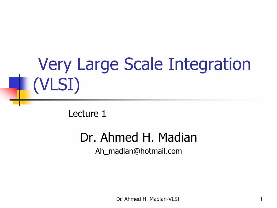
Course Objective
You’ll get a bottom-up tour of how integrated circuits are engineered. We’ll talk about
MOSFETs: how they work, how they’re built, effects of new technologies
Various design and layout techniques, from the ordinary to the most complex, for creating combinational and sequential circuits, datapaths, memories, buffers, regular logic structures, …etc.
how you tackle the problem of designing circuits with 1,000,000 gates -- you’re not in Digital IC Technique anymore!
Give different testing techniques for VLSI circuits.

Dr. Ahmed H. Madian-VLSI 3
Administrative Rules
Course schedule: Lectures:
Saturday (3rd slot), 12:30 - 13:45 Tuesday (4th slot), 14:15- 15:45
Office hours: Saturday 14:30 - 16:30 (C3.221) Teaching assistant: Eng. Mona Guindy
Grading Quizzes & Assignments: 20%
Assignment of every lecture is due the following lecture
Final exam: 80%

Dr. Ahmed H. Madian-VLSI 4
References
Anantha Chandrakasan, William J. Bowhill, Frank Fox, “Deign of high performance microprocessor circuits”
John P. Uyemura, “Introduction to VLSI circuits and systems”
Or any VLSI references
Dr. Ahmed H. Madian-VLSI 5
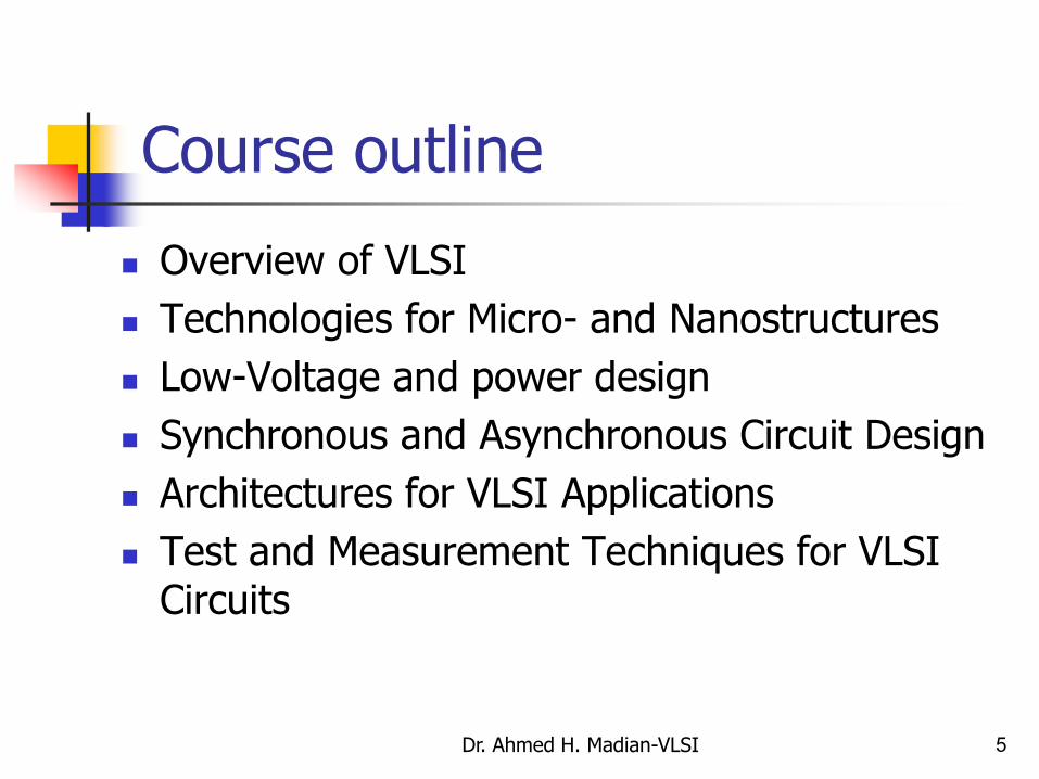
Course outline
Overview of VLSI
Technologies for Micro- and Nanostructures
Low-Voltage and power design
Synchronous and Asynchronous Circuit Design
Architectures for VLSI Applications
Test and Measurement Techniques for VLSI Circuits
Dr. Ahmed H. Madian-VLSI 6
What is VLSI?
VLSI stands for (Very Large Scale Integrated circuits)
Craver Mead of Caltech pioneered the filed of VLSI in the 1970’s.
Digital electronic integrated circuits could be viewed as a set of geometrical patterns on the surface of a silicon chip.
Complexity could thus be dealt with using the concept of repeated patterns that were fitted together in structured manner.
Dr. Ahmed H. Madian-VLSI 7
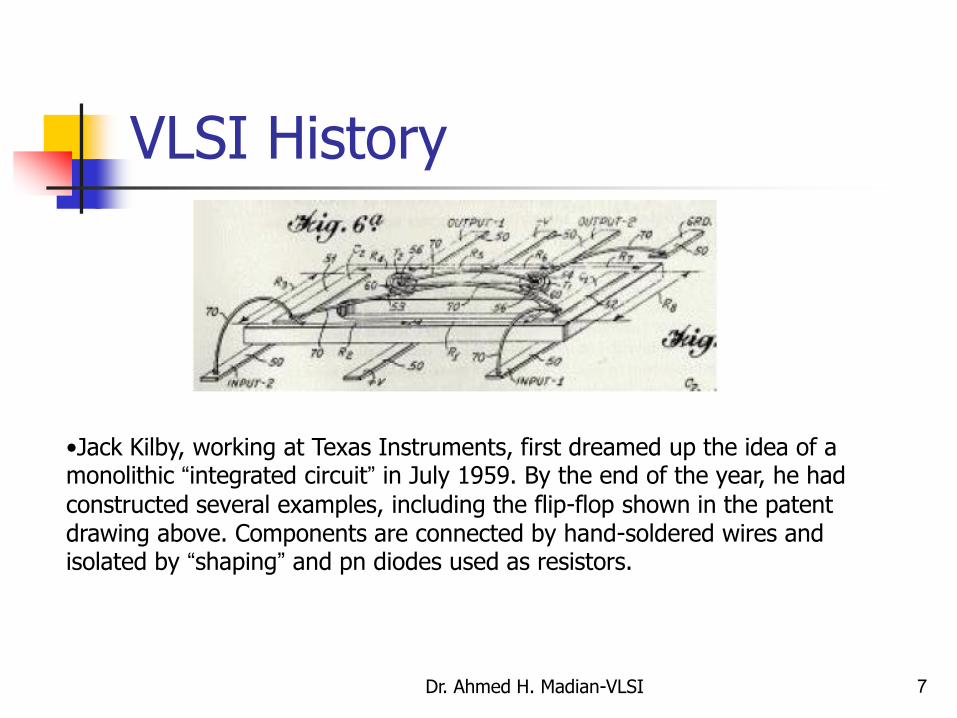
VLSI History
•Jack Kilby, working at Texas Instruments, first dreamed up the idea of a monolithic “integrated circuit” in July 1959. By the end of the year, he had
constructed several examples, including the flip-flop shown in the patent drawing above. Components are connected by hand-soldered wires and isolated by “shaping” and pn diodes used as resistors.
Dr. Ahmed H. Madian-VLSI 8
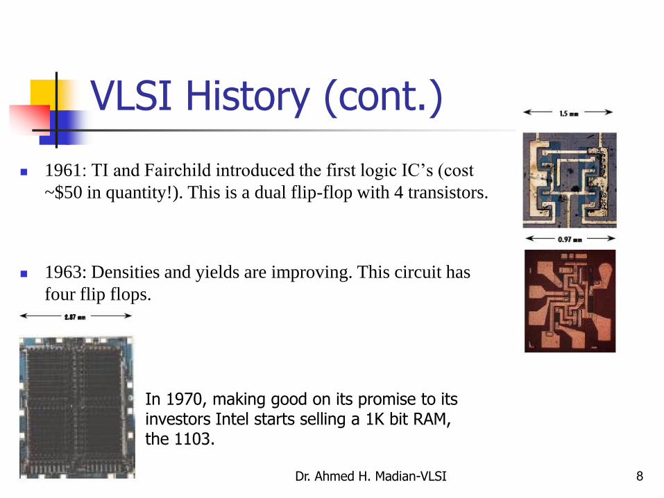
VLSI History (cont.)
1961: TI and Fairchild introduced the first logic IC’s (cost
~$50 in quantity!). This is a dual flip-flop with 4 transistors.
1963: Densities and yields are improving. This circuit has
four flip flops.
In 1970, making good on its promise to its investors Intel starts selling a 1K bit RAM, the 1103.
Dr. Ahmed H. Madian-VLSI 9
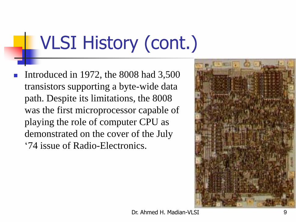
VLSI History (cont.)
Introduced in 1972, the 8008 had 3,500
transistors supporting a byte-wide data
path. Despite its limitations, the 8008
was the first microprocessor capable of
playing the role of computer CPU as
demonstrated on the cover of the July
‘74 issue of Radio-Electronics.
Dr. Ahmed H. Madian-VLSI 10
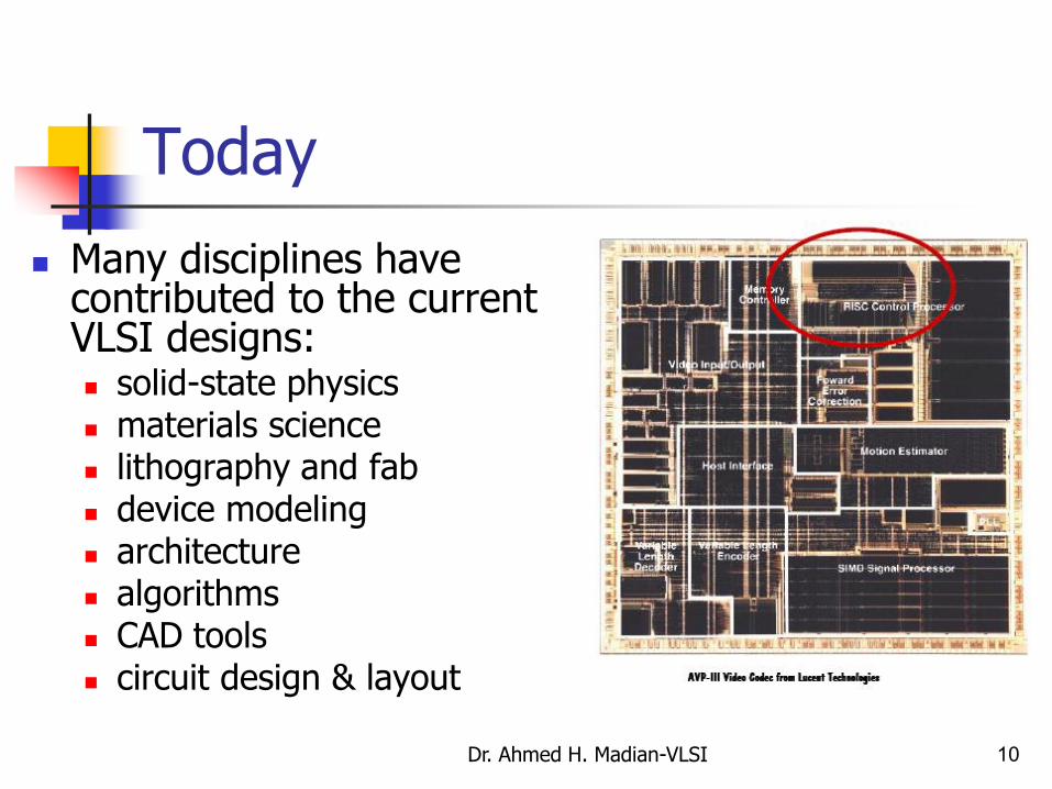
Today
Many disciplines have contributed to the current VLSI designs: solid-state physics materials science lithography and fab device modeling architecture algorithms CAD tools circuit design & layout
Dr. Ahmed H. Madian-VLSI 11
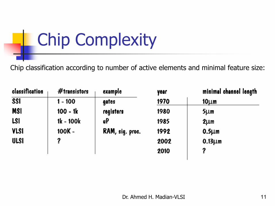
Chip Complexity
Chip classification according to number of active elements and minimal feature size:
Dr. Ahmed H. Madian-VLSI 12
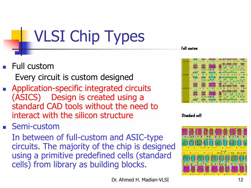
VLSI Chip Types
Full custom
Every circuit is custom designed
Application-specific integrated circuits (ASICS) Design is created using a standard CAD tools without the need to interact with the silicon structure
Semi-custom
In between of full-custom and ASIC-type circuits. The majority of the chip is designed using a primitive predefined cells (standard cells) from library as building blocks.
Dr. Ahmed H. Madian-VLSI 13
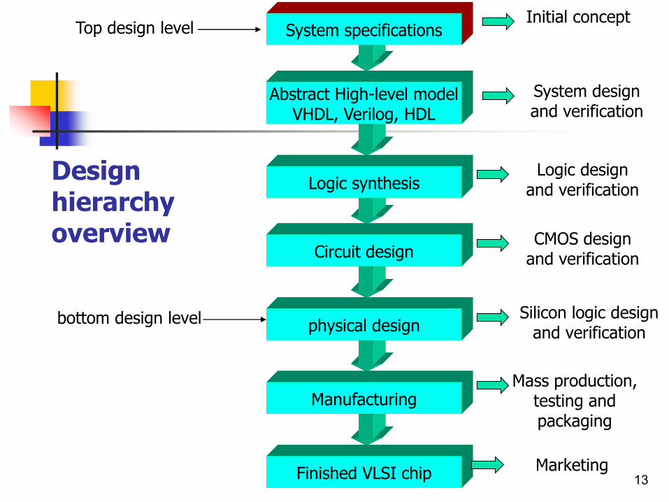
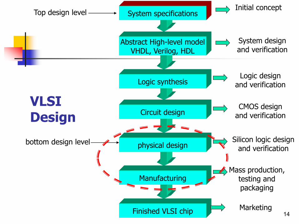
Design hierarchy overview
System specifications
Abstract High-level modelVHDL, Verilog, HDL
Logic synthesis
Circuit design
physical design
Manufacturing
Finished VLSI chip
Top design level
bottom design level
Initial concept
System design and verification
Logic design and verification
CMOS design and verification
Silicon logic design and verification
Mass production, testing and packaging
Marketing
Dr. Ahmed H. Madian-VLSI 14
VLSI Design
System specifications
Abstract High-level modelVHDL, Verilog, HDL
Logic synthesis
Circuit design
physical design
Manufacturing
Finished VLSI chip
Top design level
bottom design level
Initial concept
System design and verification
Logic design and verification
CMOS design and verification
Silicon logic design and verification
Mass production, testing and packaging
Marketing
Dr. Ahmed H. Madian-VLSI 15
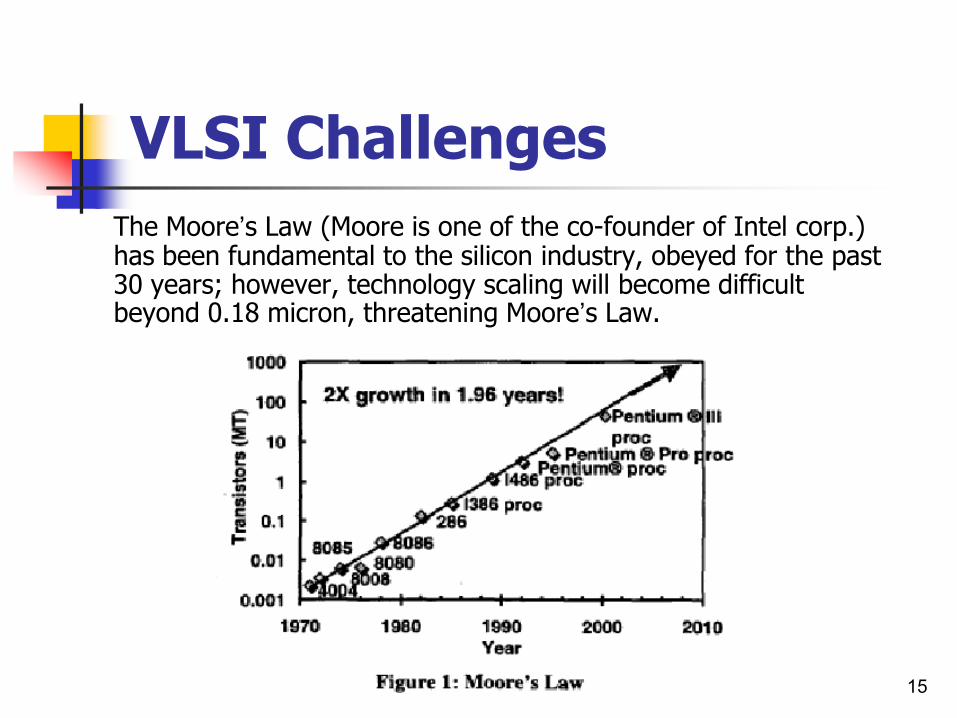
VLSI Challenges
The Moore’s Law (Moore is one of the co-founder of Intel corp.) has been fundamental to the silicon industry, obeyed for the past 30 years; however, technology scaling will become difficult beyond 0.18 micron, threatening Moore’s Law.

Dr. Ahmed H. Madian-VLSI 16
Scaled-down Transistors
The principle of constant-filedscaling lies in scaling the devicevoltages and the device dimensions(both horizontal and vertical) by thesame factor , k (>1) , such that theelectric filed remains unchanged.
Dr. Ahmed H. Madian-VLSI 17
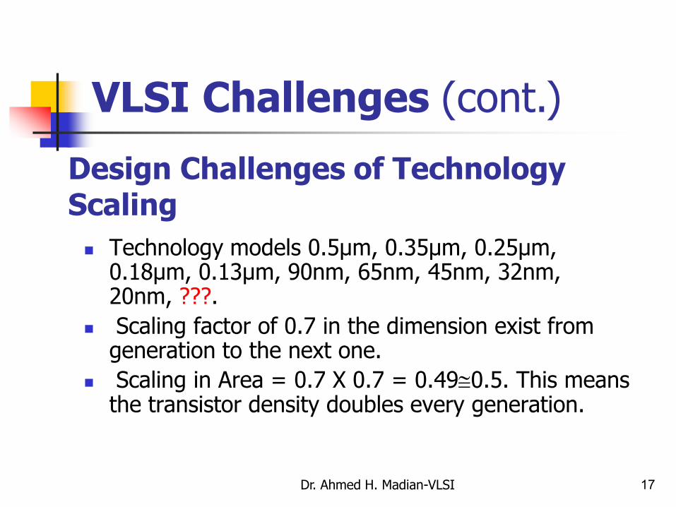
Design Challenges of TechnologyScaling
Technology models 0.5µm, 0.35µm, 0.25µm, 0.18µm, 0.13µm, 90nm, 65nm, 45nm, 32nm, 20nm, ???.
Scaling factor of 0.7 in the dimension exist from generation to the next one.
Scaling in Area = 0.7 X 0.7 = 0.490.5. This means the transistor density doubles every generation.
VLSI Challenges (cont.)
Dr. Ahmed H. Madian-VLSI 18
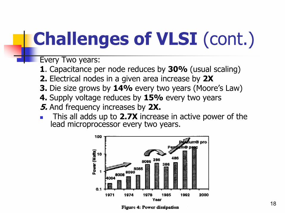
Challenges of VLSI (cont.)Every Two years:1. Capacitance per node reduces by 30% (usual scaling)2. Electrical nodes in a given area increase by 2X3. Die size grows by 14% every two years (Moore’s Law)4. Supply voltage reduces by 15% every two years5. And frequency increases by 2X. This all adds up to 2.7X increase in active power of the
lead microprocessor every two years.
Revision on MOSFET Fabrication procedure
Dr. Ahmed H. Madian-VLSI 19
Dr. Ahmed H. Madian-VLSI 20
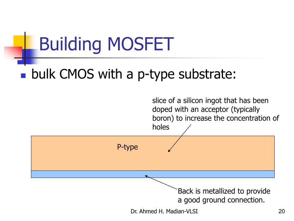
Building MOSFET
bulk CMOS with a p-type substrate:
slice of a silicon ingot that has been doped with an acceptor (typically boron) to increase the concentration of holes
P-type
Back is metallized to providea good ground connection.

Dr. Ahmed H. Madian-VLSI 21
Building MOSFET (cont.)
Next, a “thick” layer of silicon dioxide, called field oxide, is formed on the surface by oxidation in wet oxygen. This is then etched to expose surface where we want to make a MOSFET:

Dr. Ahmed H. Madian-VLSI 22
Building MOSFET (cont.)
Now grow a “thin” layer of silicon dioxide, called gate oxide, on the surface by exposing the wafer to dry oxygen.
Dr. Ahmed H. Madian-VLSI 23
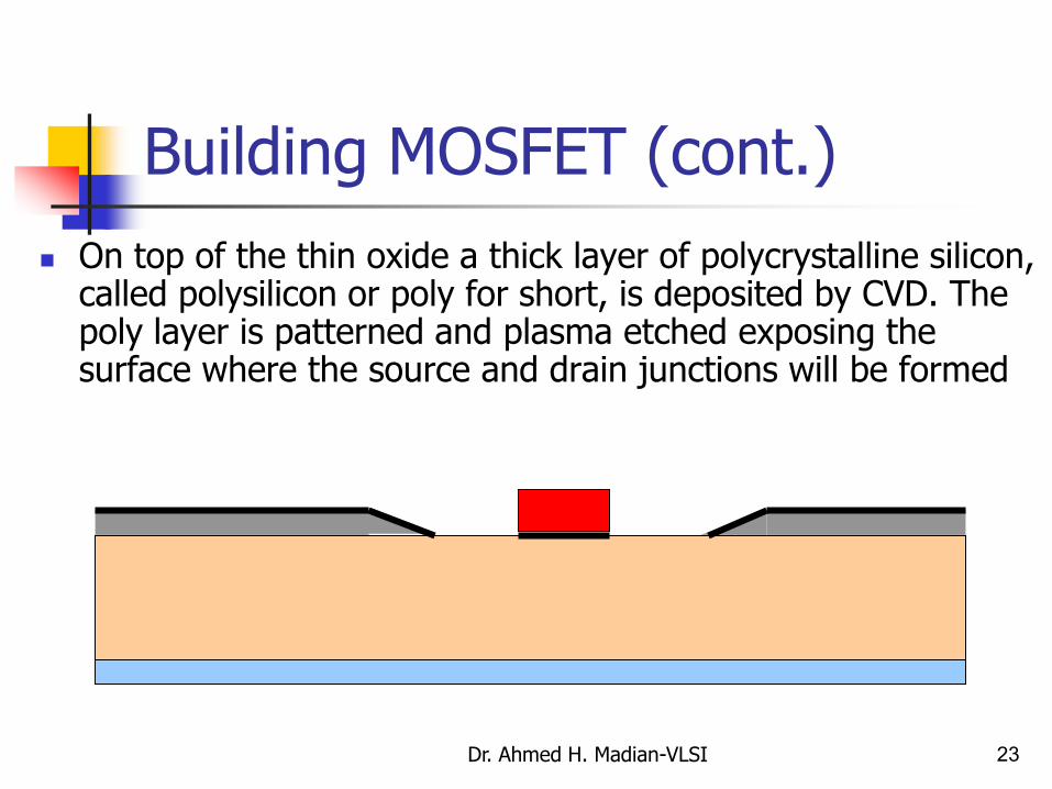
Building MOSFET (cont.)
On top of the thin oxide a thick layer of polycrystalline silicon, called polysilicon or poly for short, is deposited by CVD. The poly layer is patterned and plasma etched exposing the surface where the source and drain junctions will be formed
Dr. Ahmed H. Madian-VLSI 24
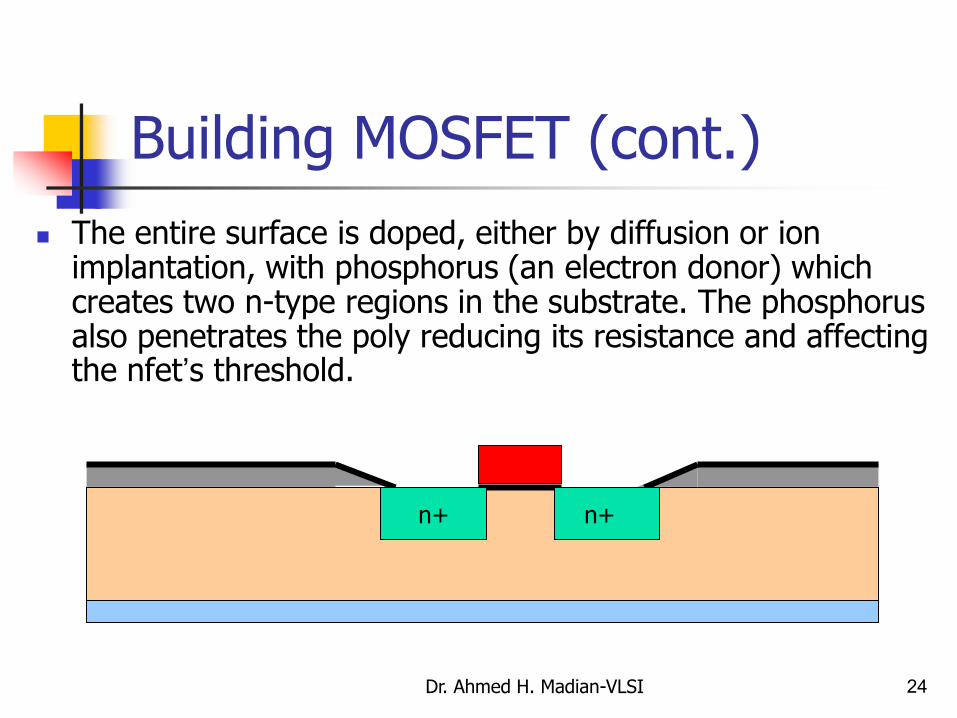
Building MOSFET (cont.)
The entire surface is doped, either by diffusion or ion implantation, with phosphorus (an electron donor) which creates two n-type regions in the substrate. The phosphorus also penetrates the poly reducing its resistance and affecting the nfet’s threshold.
n+ n+

Dr. Ahmed H. Madian-VLSI 25
Building MOSFET (cont.)
Finally an intermediate oxide layer is grown and then reflowed to flatten its surface. Holes are etched in the oxide (where contacts to poly/diff are wanted) and aluminum deposited, patterned and etched.
n+ n+
Dr. Ahmed H. Madian-VLSI 26
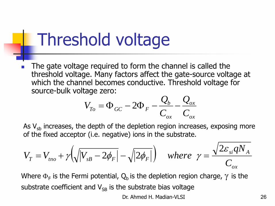
Threshold voltage
The gate voltage required to form the channel is called the threshold voltage. Many factors affect the gate-source voltage at which the channel becomes conductive. Threshold voltage for source-bulk voltage zero:
ox
ox
ox
bFGCTo
C
Q
C
QV 2
As Vsb increases, the depth of the depletion region increases, exposing more of the fixed acceptor (i.e. negative) ions in the substrate.
ox
Asi
FFsBtnoTC
qNwhereVVV
222
Where F is the Fermi potential, Qb is the depletion region charge, is the
substrate coefficient and VSB is the substrate bias voltage

Dr. Ahmed H. Madian-VLSI 27
Channel-Length modulation
Dr. Ahmed H. Madian-VLSI 28
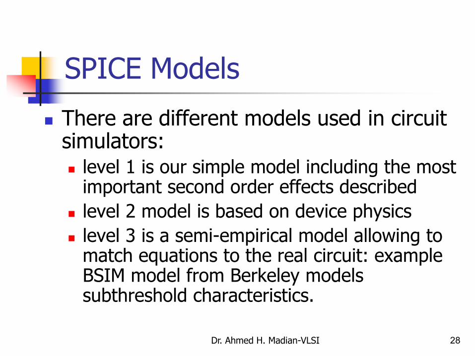
SPICE Models
There are different models used in circuit simulators: level 1 is our simple model including the most
important second order effects described
level 2 model is based on device physics
level 3 is a semi-empirical model allowing to match equations to the real circuit: example BSIM model from Berkeley models subthreshold characteristics.
Dr. Ahmed H. Madian-VLSI 29
Physical design
CMOS ICs are electronic switching networks that are created on small area of silicon wafer using complex set of physical and chemical processes.
A primary task for VLSI designer is to translate circuit schematics into silicon form (this process is called physical design)

Dr. Ahmed H. Madian-VLSI 30
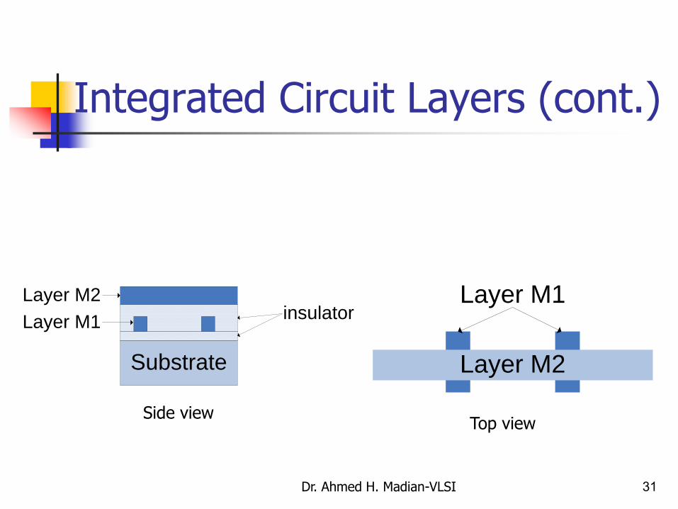
Integrated Circuit Layers
ICs are made by stacking different layers of materials in a specific order to form three dimensional structures that act as an electronic switching network. Substrate
Layer M1
Insulator
SubstrateM1 M1
Top viewSide view
Dr. Ahmed H. Madian-VLSI 31
Integrated Circuit Layers (cont.)
Layer M2
Layer M1
Substrate
insulator
Layer M2
Layer M1
Top viewSide view
Dr. Ahmed H. Madian-VLSI 32
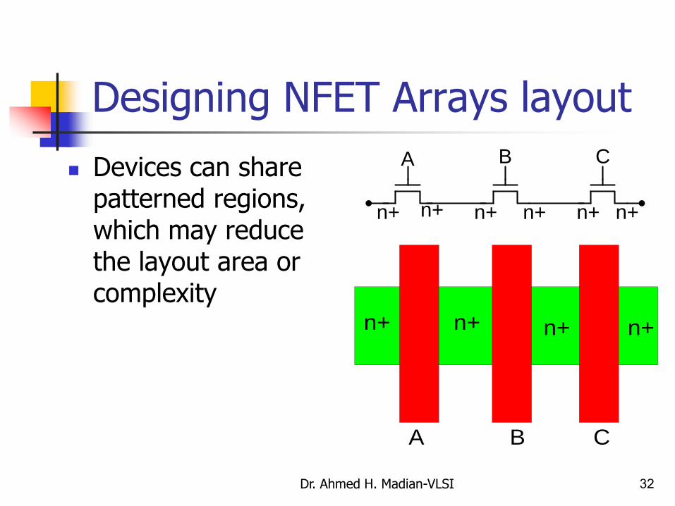
Designing NFET Arrays layout
Devices can share patterned regions, which may reduce the layout area or complexity
A B C
n+ n+ n+ n+ n+ n+
A B C
n+ n+ n+ n+
Dr. Ahmed H. Madian-VLSI 33
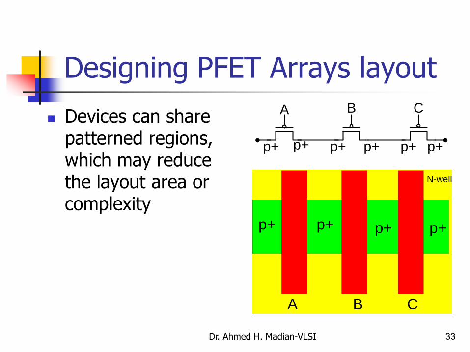
Designing PFET Arrays layout
Devices can share patterned regions, which may reduce the layout area or complexity
A B C
p+ p+ p+ p+ p+ p+
A B C
p+ p+ p+ p+
N-well
Dr. Ahmed H. Madian-VLSI 34
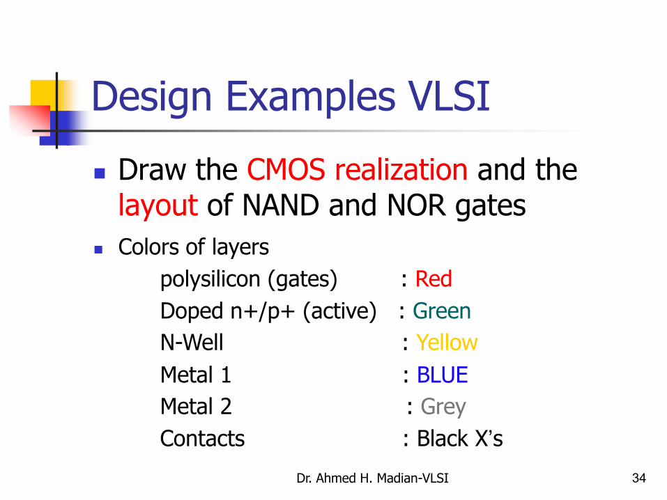
Design Examples VLSI
Draw the CMOS realization and the layout of NAND and NOR gates
Colors of layers
polysilicon (gates) : Red
Doped n+/p+ (active) : Green
N-Well : Yellow
Metal 1 : BLUE
Metal 2 : Grey
Contacts : Black X’s
Dr. Ahmed H. Madian-VLSI 35
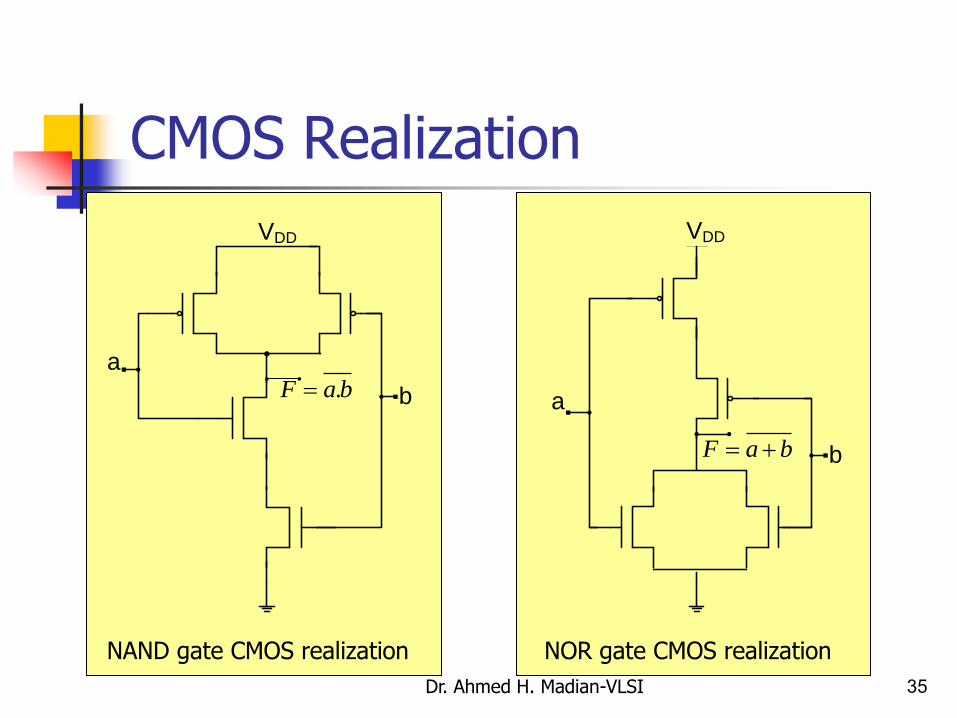
CMOS Realization
NAND gate CMOS realization
VDD
a
bbaF .
NOR gate CMOS realization
VDD
a
bbaF

Dr. Ahmed H. Madian-VLSI 36
NAND FET Layout
PFET
NFET
N-WELL
P+ P+ P+GateGate
Gate GateN+ N+ N+
VDD
a
b

Dr. Ahmed H. Madian-VLSI 37
NAND FET Layout (cont.)VDD
a
b
PFET
NFET
VDD
X X
X
GND

Dr. Ahmed H. Madian-VLSI 38
NAND FET Layout (cont.)
VDD
a
b
PFET
NFET
VDD
X
X
GND
X
OUT
a bX
X
Dr. Ahmed H. Madian-VLSI 39
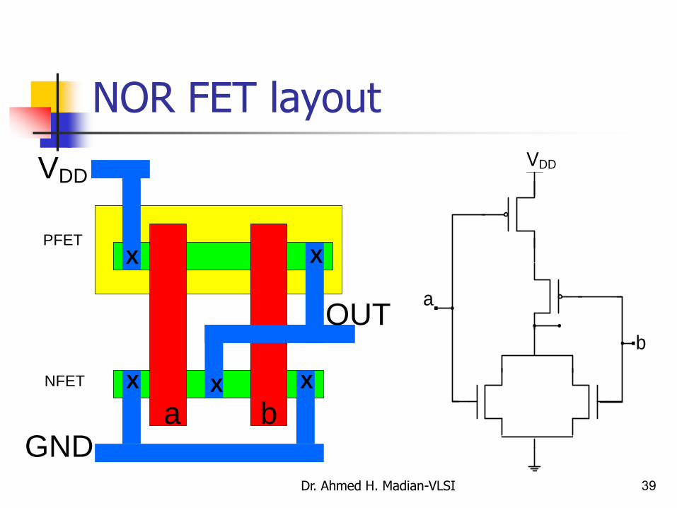
NOR FET layout
VDD
a
b
PFET
NFET
VDD
X
X
GND
X
X
OUT
a bX

Dr. Ahmed H. Madian-VLSI 40
Design Examples VLSI
Draw the pass transistor realization and the layout of MUX 4:1
Colors of layers
polysilicon (gates) : Red
Doped n+/p+ (active) : Green
N-Well : Yellow
Metal 1 : BLUE
Metal 2 : Grey
Contacts : Black X’s
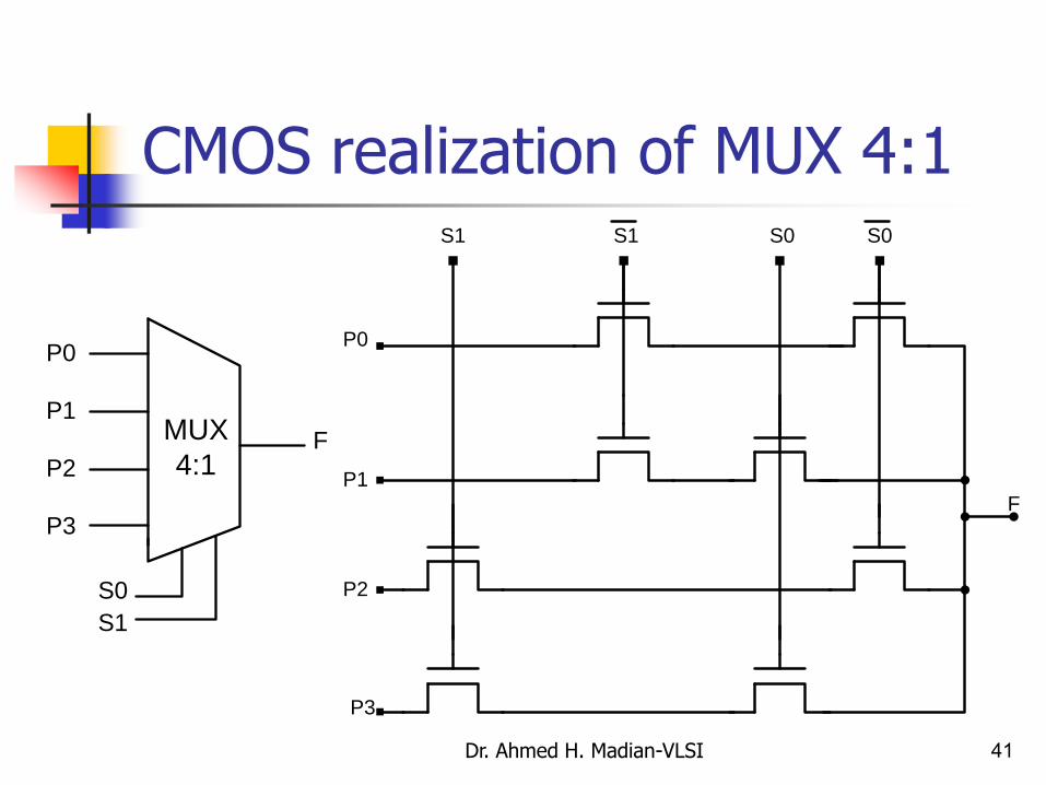
Dr. Ahmed H. Madian-VLSI 41
CMOS realization of MUX 4:1
P0
P1
P2
P3
S1 S1 S0S0
F
P0
P1
P2
P3
MUX
4:1
S0
S1
F
Dr. Ahmed H. Madian-VLSI 42
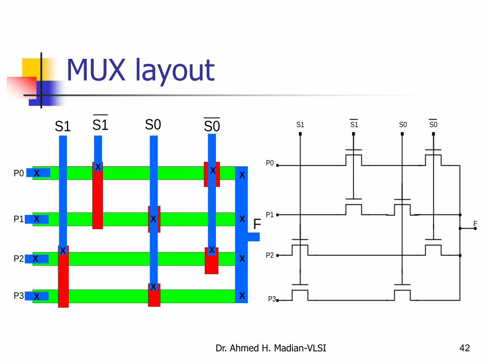
MUX layout
F
S1
X
X
X
X
X
XX
X
X
X
P0
P1
P2
P3
X
X
X
X
S1 S0S0
P0
P1
P2
P3
S1 S1 S0S0
F

Dr. Ahmed H. Madian-VLSI 43
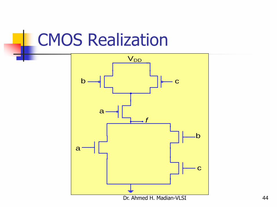
Design Examples VLSI
Draw the CMOS realization and the layout of logic function
Colors of layers
polysilicon (gates) : Red
Doped n+/p+ (active) : Green
N-Well : Yellow
Metal 1 : BLUE
Metal 2 : Grey
Contacts : Black X’s
cbaf .
Dr. Ahmed H. Madian-VLSI 44
CMOS RealizationVDD
a
b
c
a
b c
f

Dr. Ahmed H. Madian-VLSI 45
Logic function Layout
PFET
NFET
N-Well
P+
N+
VDD
a
b
c
a
b c
f
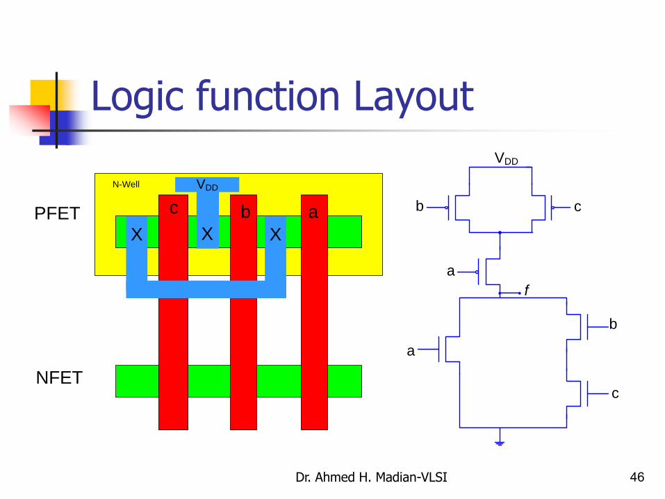
Dr. Ahmed H. Madian-VLSI 46
Logic function Layout
PFET
NFET
N-Well VDD
XX X
bc a
VDD
a
b
c
a
b c
f

Dr. Ahmed H. Madian-VLSI 47
Logic function Layout
PFET
NFET
N-Well VDD
XX X
X X
GND
X
X
f
abc
VDD
a
b
c
a
b c
f

Dr. Ahmed H. Madian-VLSI 48
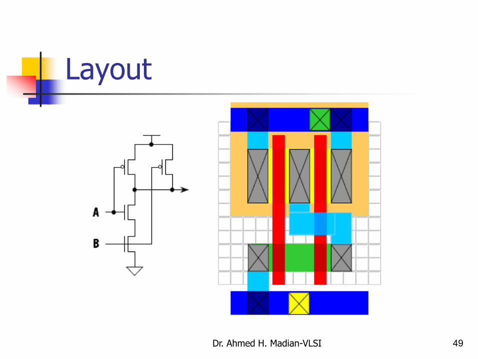
Layout Rules
Layout rules are the common language between design and process engineers
conservative rules absorb process disturbances and variations layout rules must be respected by the designer layout rules reflect the limits of a process, they describe:
minimal distance, overlap minimal width (e.x. channel length, λ)
layout readability is improved using colors: metal blue polysilicium red n-diffusion green p-diffusion yellow n-well brown contact, via black
Dr. Ahmed H. Madian-VLSI 49
Layout
Dr. Ahmed H. Madian-VLSI 50
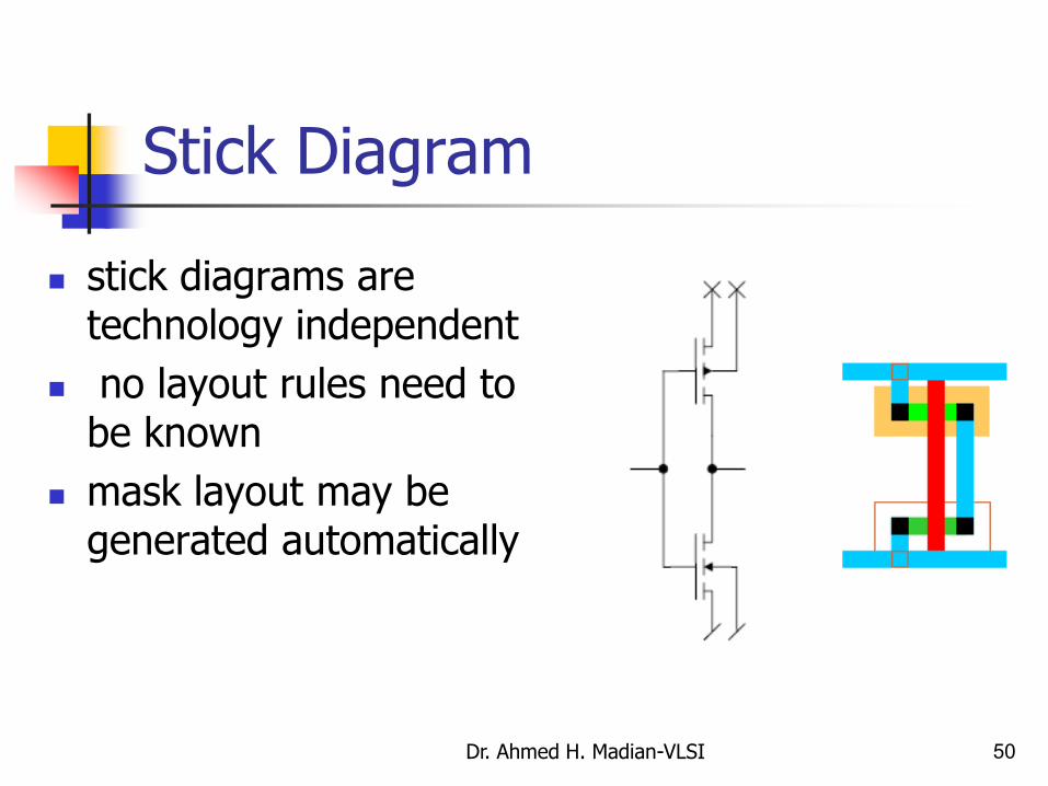
Stick Diagram
stick diagrams are technology independent
no layout rules need to be known
mask layout may be generated automatically
Dr. Ahmed H. Madian-VLSI 51
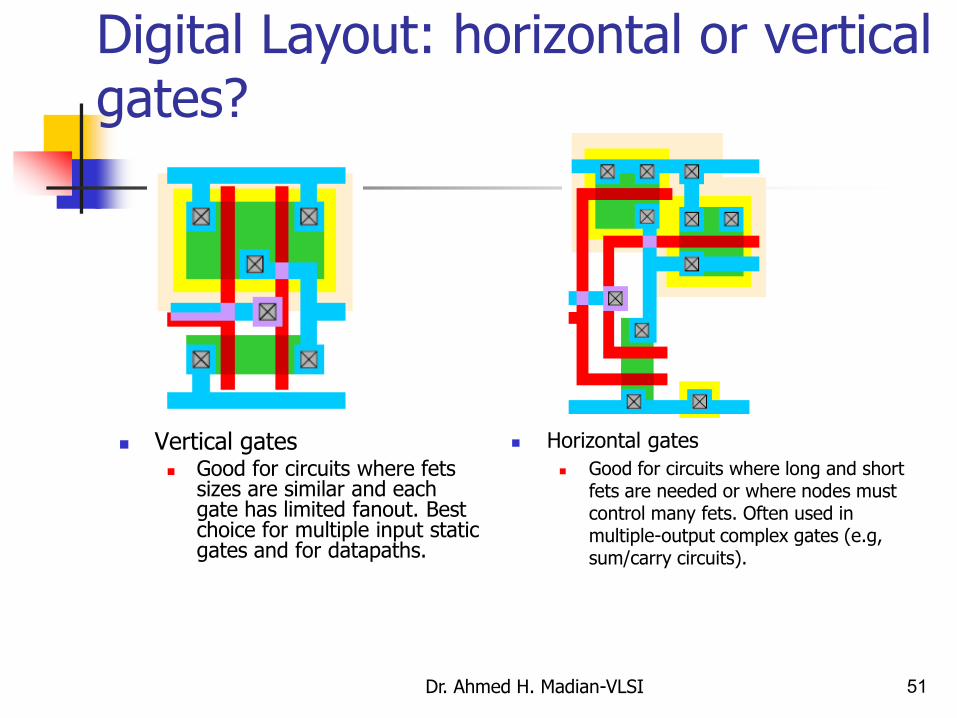
Digital Layout: horizontal or vertical gates?
Vertical gates Good for circuits where fets
sizes are similar and each gate has limited fanout. Best choice for multiple input static gates and for datapaths.
Horizontal gates
Good for circuits where long and short fets are needed or where nodes must control many fets. Often used in multiple-output complex gates (e.g, sum/carry circuits).

Dr. Ahmed H. Madian-VLSI 52
Eliminating Gaps
Dr. Ahmed H. Madian-VLSI 53
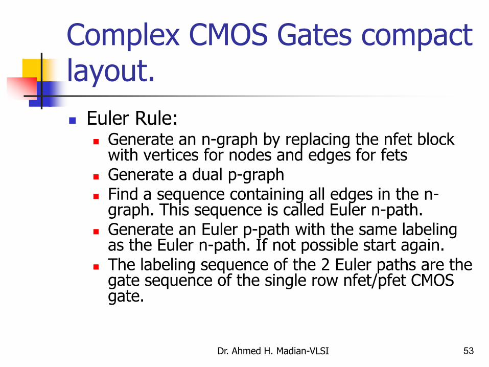
Complex CMOS Gates compact layout.
Euler Rule: Generate an n-graph by replacing the nfet block
with vertices for nodes and edges for fets Generate a dual p-graph Find a sequence containing all edges in the n-
graph. This sequence is called Euler n-path. Generate an Euler p-path with the same labeling
as the Euler n-path. If not possible start again. The labeling sequence of the 2 Euler paths are the
gate sequence of the single row nfet/pfet CMOS gate.
Dr. Ahmed H. Madian-VLSI 54
Draw the most compact layout for the following logic function using Euler’s rule.
F= A.(B+C)
Example

Dr. Ahmed H. Madian-VLSI 55
Solution
VDD
A
A
B
C
C B
N1
F
N2
GND
F
N2
GND
N1
FVDD
A
BC
A B C
Dr. Ahmed H. Madian-VLSI 56
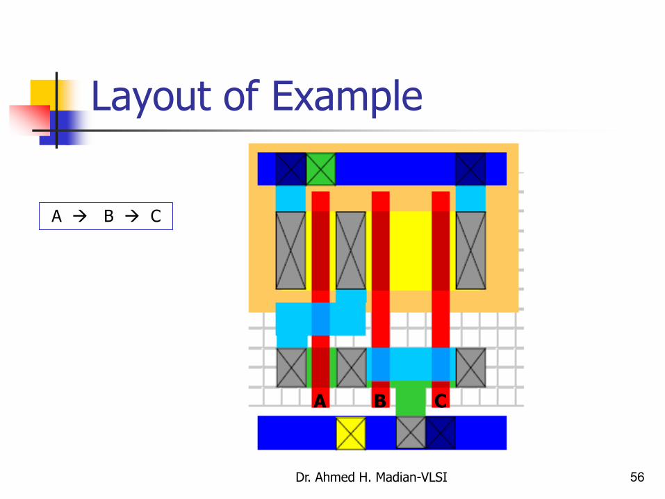
Layout of Example
A B C
A B C
Dr. Ahmed H. Madian-VLSI 57
Thanks
Revision sheet will be soon available on the web site
you must solve it
Download one of the layout tools and practice on the lecture examples