Embed Size (px)
Citation preview
University of Tehran 2
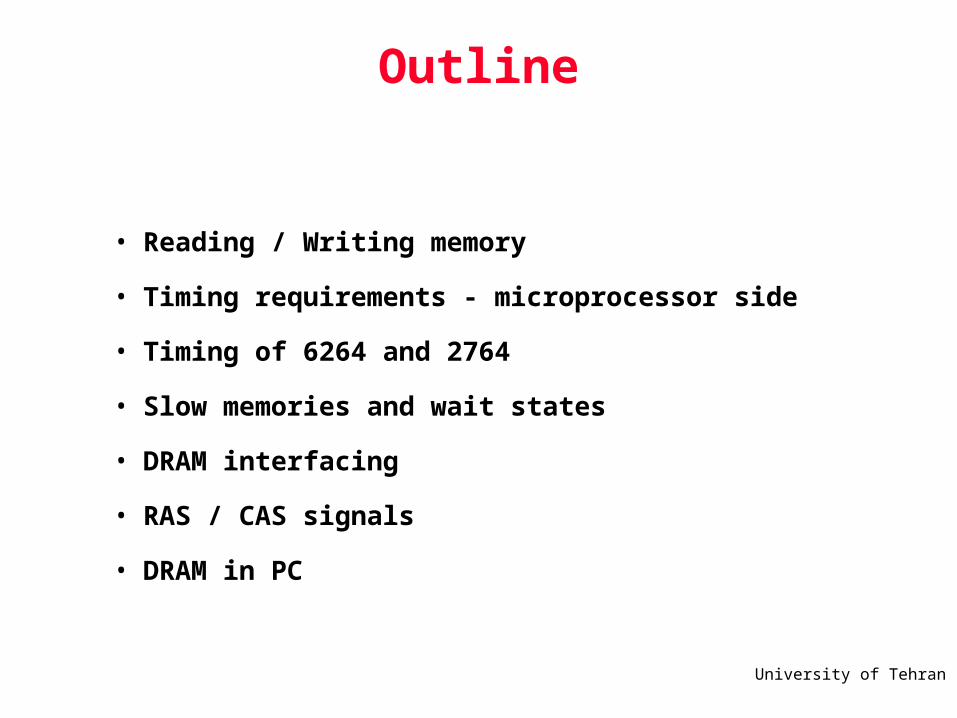
Outline
• Reading / Writing memory
• Timing requirements - microprocessor side
• Timing of 6264 and 2764
• Slow memories and wait states
• DRAM interfacing
• RAS / CAS signals
• DRAM in PC
University of Tehran 3
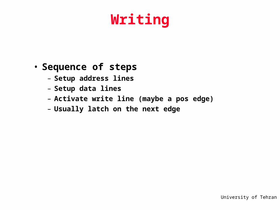
Writing
• Sequence of steps– Setup address lines
– Setup data lines
– Activate write line (maybe a pos edge)
– Usually latch on the next edge
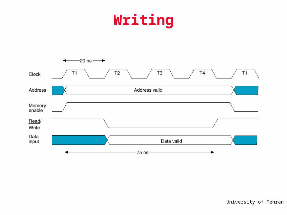
University of Tehran 4
Writing
University of Tehran 5
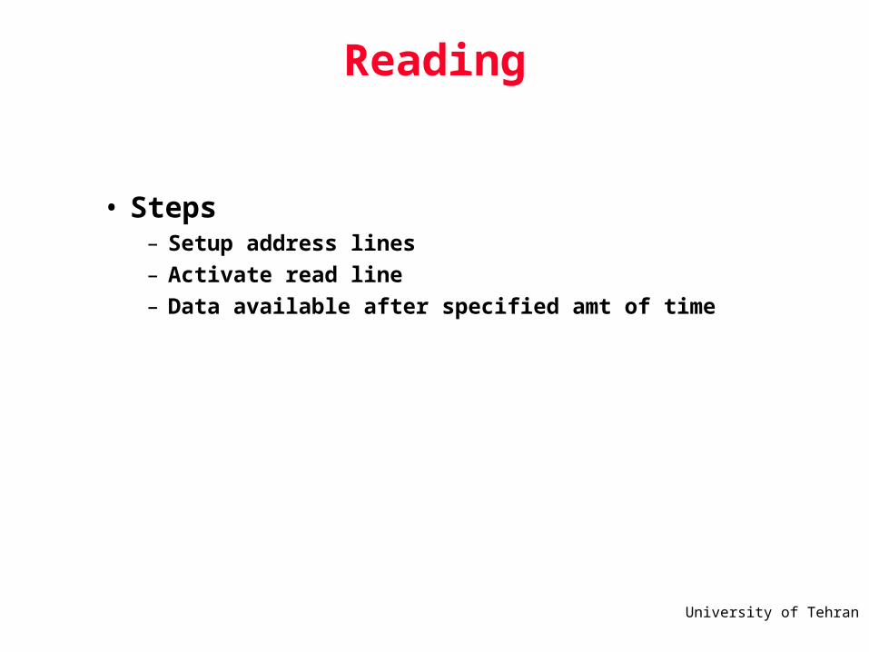
Reading
• Steps– Setup address lines
– Activate read line
– Data available after specified amt of time
University of Tehran 6
Reading
University of Tehran 7
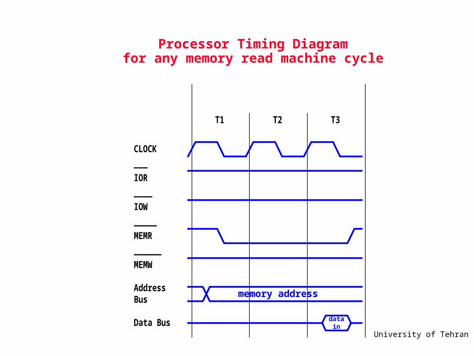
Processor Timing Diagramfor any memory read machine cycle
IOR
IOW
MEMR
MEMW
___
____
_____
______
AddressBus
Data Bus
T1 T2 T3
CLOCK
memory address
datain
University of Tehran 8
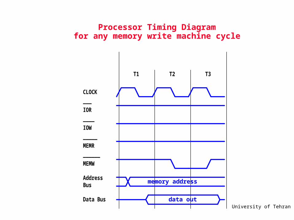
Processor Timing Diagramfor any memory write machine cycle
IOR
IOW
MEMR
MEMW
___
____
_____
______
AddressBus
Data Bus
T1 T2 T3
CLOCK
memory address
data out
University of Tehran 9
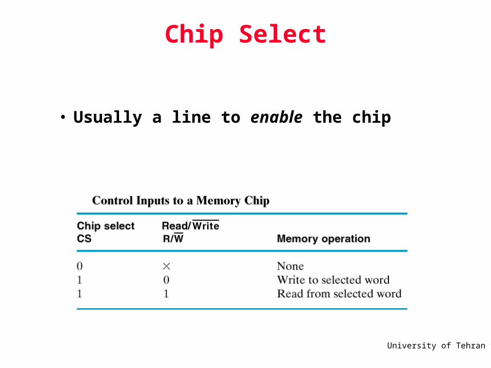
Chip Select
• Usually a line to enable the chip
University of Tehran 10
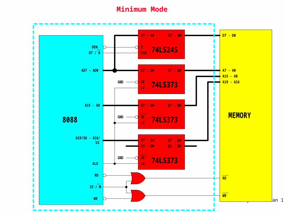
Minimum Mode
MEMORY
D7 - D0 Q7 - Q0
OE
LE 74LS373
D7 - D0 Q7 - Q0
OE
LE 74LS3738088
AD7 - AD0
A15 - A8
A19/S6 - A16/S3
DEN
DT / R
IO / M
RD
WR
ALE
D7 - D4 Q7 - Q4
OE
LE 74LS373
D3 - D0 Q3 - Q0
GND
GND
GND
D7 - D0A7 - A0 B7 - B0
E
DIR 74LS245
A7 - A0
A15 - A8
A19 - A16
RD
WR
University of Tehran 11
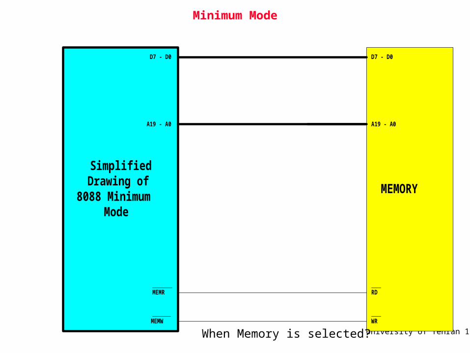
Minimum Mode
MEMORY
D7 - D0
A19 - A0
RD
WR
SimplifiedDrawing of
8088 MinimumMode
D7 - D0
A19 - A0
MEMR
MEMW
When Memory is selected?
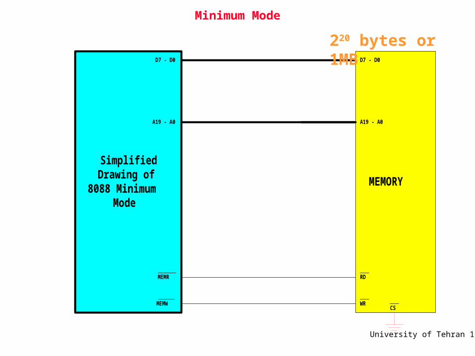
University of Tehran 12
Minimum Mode
MEMORY
D7 - D0
A19 - A0
RD
WR
SimplifiedDrawing of
8088 MinimumMode
D7 - D0
A19 - A0
MEMR
MEMWCS
220 bytes or 1MB
University of Tehran 13
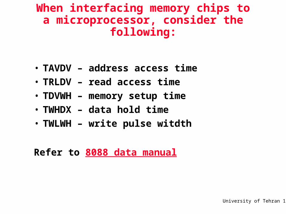
When interfacing memory chips to a microprocessor, consider the following:
• TAVDV – address access time
• TRLDV – read access time
• TDVWH – memory setup time
• TWHDX – data hold time
• TWLWH – write pulse witdth
Refer to 8088 data manual
University of Tehran 14
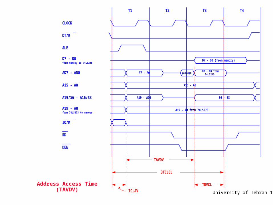
Address Access Time (TAVDV)
ALE
T1
CLOCK
T2 T3 T4
AD7 - AD0
A15 - A8
A19/S6 - A16/S3
DT/R __
IO/M __
____
RD
DEN______
A19 - A0from 74LS373 to memory
A15 - A8
A19 - A16 S6 - S3
A19 - A0 from 74LS373
D7 - D0from memory to 74LS245
D7 - D0 (from memory)
A7 - A0 D7 - D0 from74LS245
garbage
TAVDV
3TCLCL
TCLAV
TDVCL

University of Tehran 15
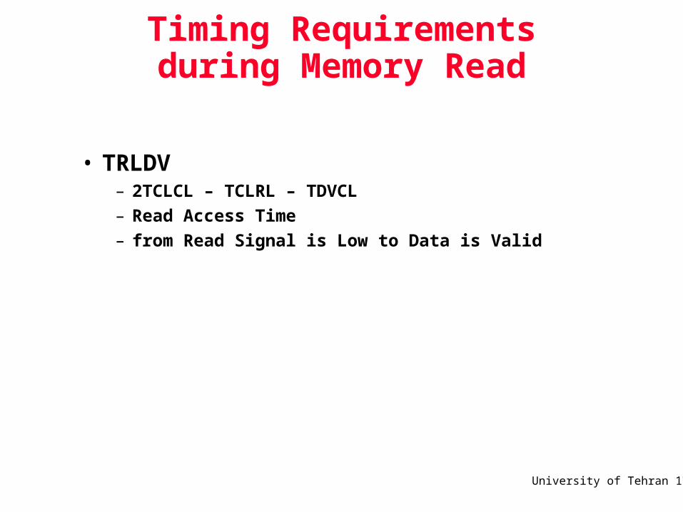
Timing Requirements during Memory Read
• TAVDV– 3TCLCL – TCLAV – TDVCL
– Address Access Time
– from Address is Valid to Data is Valid
University of Tehran 16
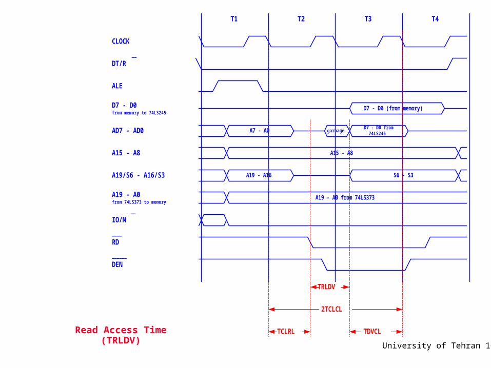
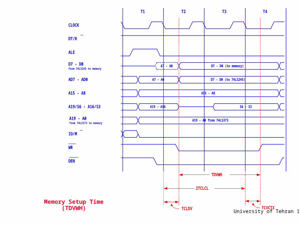
Read Access Time (TRLDV)
ALE
T1
CLOCK
T2 T3 T4
AD7 - AD0
A15 - A8
A19/S6 - A16/S3
DT/R __
IO/M __
____
RD
DEN______
A19 - A0from 74LS373 to memory
A15 - A8
A19 - A16 S6 - S3
A19 - A0 from 74LS373
D7 - D0from memory to 74LS245
D7 - D0 (from memory)
A7 - A0 D7 - D0 from74LS245
garbage
TRLDV
2TCLCL
TDVCLTCLRL
University of Tehran 17
Timing Requirements during Memory Read
• TRLDV– 2TCLCL – TCLRL – TDVCL
– Read Access Time
– from Read Signal is Low to Data is Valid
University of Tehran 18
Memory Setup Time (TDVWH)
ALE
T1
CLOCK
T2 T3 T4
AD7 - AD0
A15 - A8
A19/S6 - A16/S3
DT/R __
IO/M __
_____
WR
DEN______
A19 - A0from 74LS373 to memory
A15 - A8
A19 - A16 S6 - S3
A19 - A0 from 74LS373
A7 - A0 D7 - D0 (to 74LS245)
D7 - D0from 74LS245 to memory
D7 - D0 (to memory)A7 - A0
2TCLCL
TDVWH
TCLDV TCVCTX
University of Tehran 19
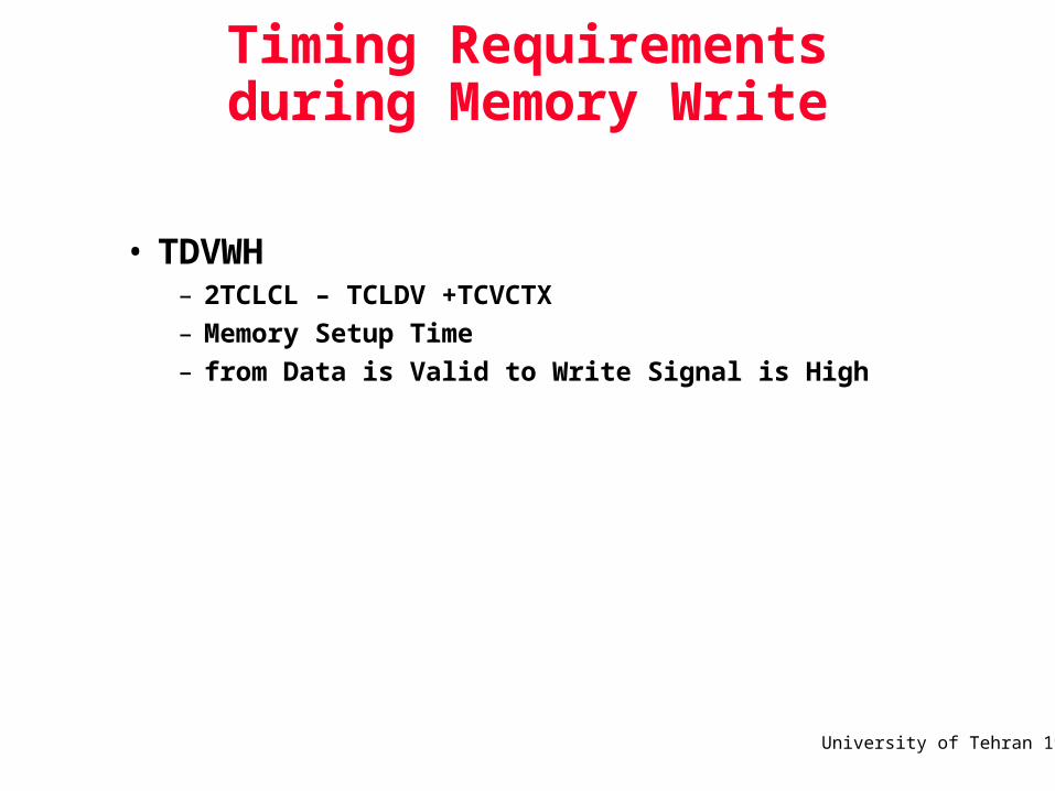
Timing Requirements during Memory Write
• TDVWH– 2TCLCL – TCLDV +TCVCTX
– Memory Setup Time
– from Data is Valid to Write Signal is High
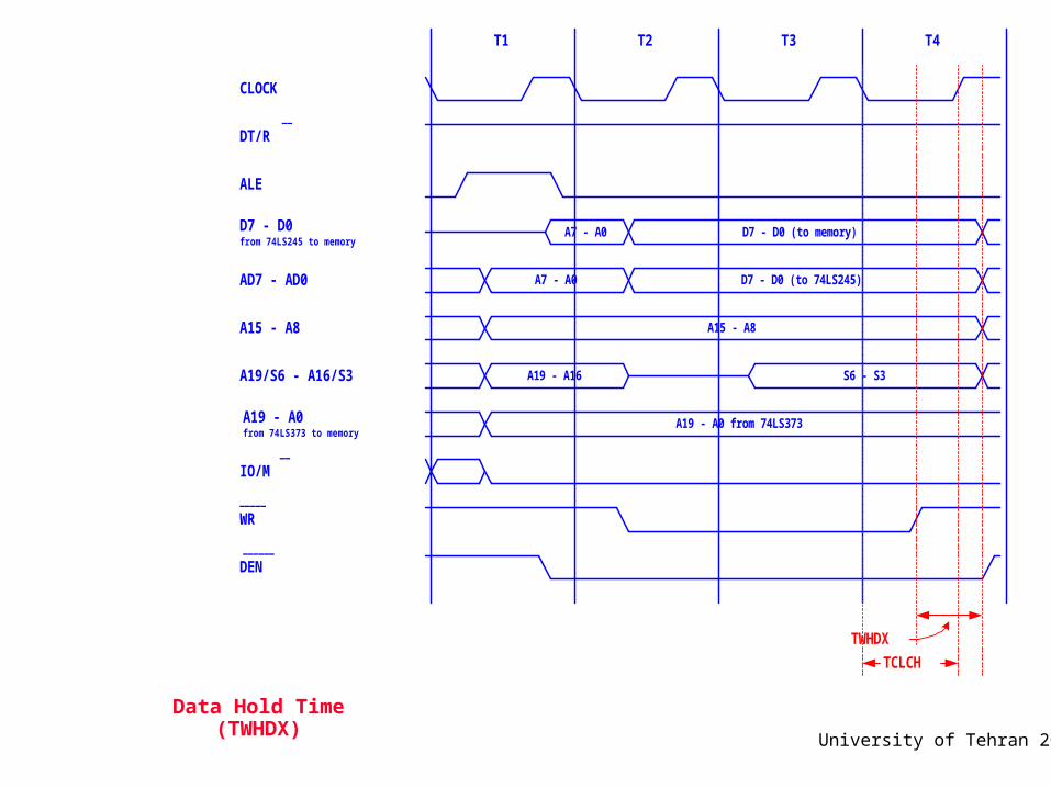
University of Tehran 20Data Hold Time (TWHDX)
ALE
T1
CLOCK
T2 T3 T4
AD7 - AD0
A15 - A8
A19/S6 - A16/S3
DT/R __
IO/M __
_____
WR
DEN______
A19 - A0from 74LS373 to memory
A15 - A8
A19 - A16 S6 - S3
A19 - A0 from 74LS373
A7 - A0 D7 - D0 (to 74LS245)
D7 - D0from 74LS245 to memory
D7 - D0 (to memory)A7 - A0
TWHDX
TCLCH
University of Tehran 21
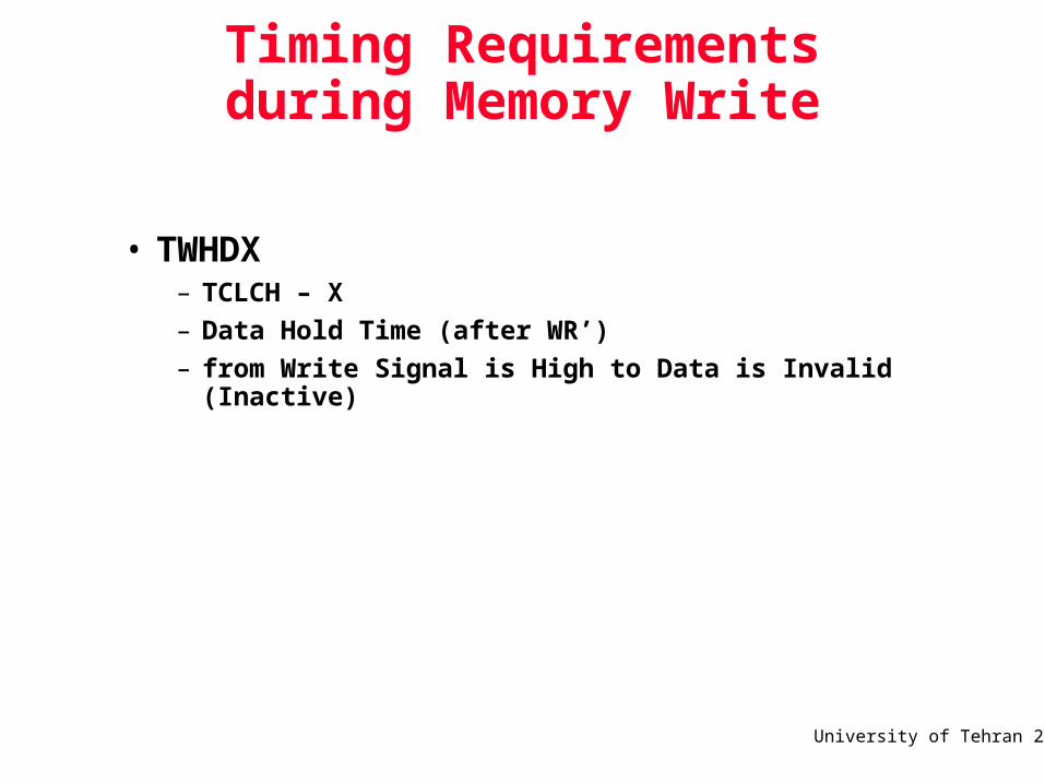
Timing Requirements during Memory Write
• TWHDX– TCLCH – X
– Data Hold Time (after WR’)
– from Write Signal is High to Data is Invalid (Inactive)
University of Tehran 22
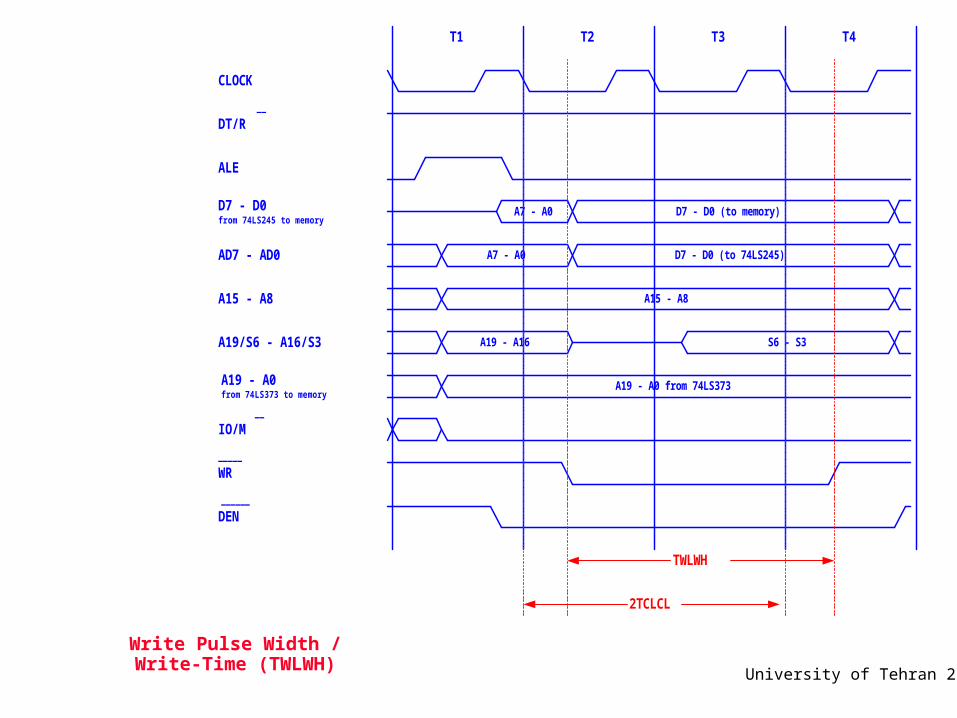
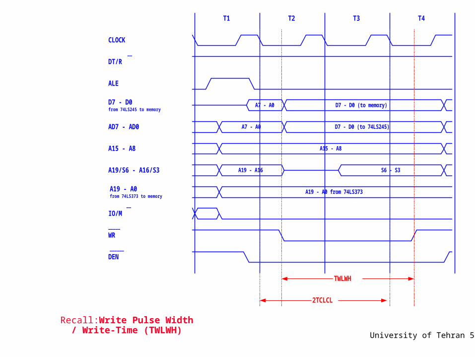
Write Pulse Width / Write-Time (TWLWH)
ALE
T1
CLOCK
T2 T3 T4
AD7 - AD0
A15 - A8
A19/S6 - A16/S3
DT/R __
IO/M __
_____
WR
DEN______
A19 - A0from 74LS373 to memory
A15 - A8
A19 - A16 S6 - S3
A19 - A0 from 74LS373
A7 - A0 D7 - D0 (to 74LS245)
D7 - D0from 74LS245 to memory
D7 - D0 (to memory)A7 - A0
TWLWH
2TCLCL
University of Tehran 23
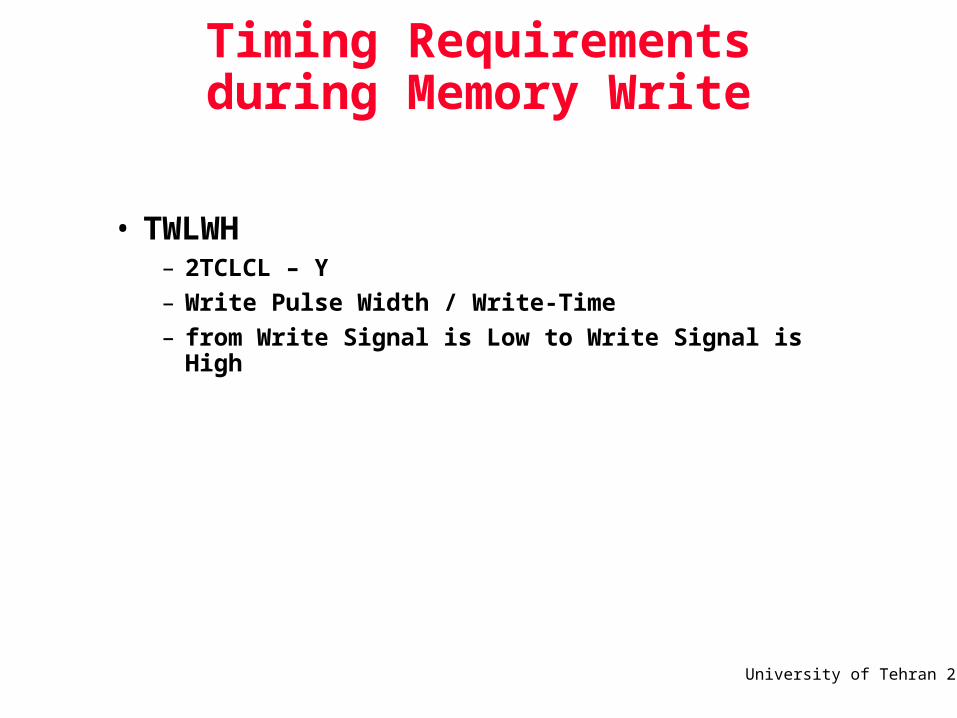
Timing Requirements during Memory Write
• TWLWH– 2TCLCL – Y
– Write Pulse Width / Write-Time
– from Write Signal is Low to Write Signal is High
University of Tehran 24
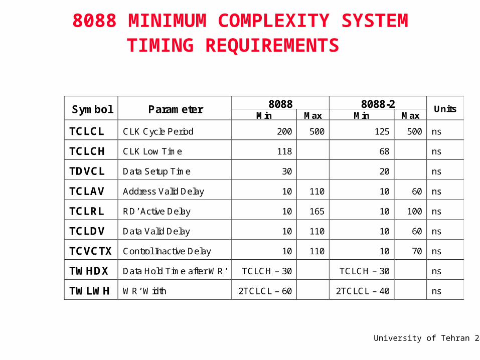
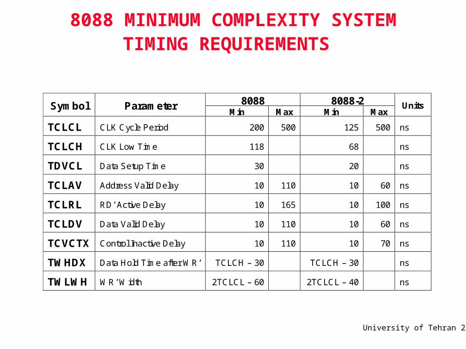
8088 MINIMUM COMPLEXITY SYSTEM TIMING REQUIREMENTS
8088 8088-2 Symbol Parameter Min Max Min Max
Units
TCLCL CLK Cycle Period 200 500 125 500 ns
TCLCH CLK Low Time 118 68 ns
TDVCL Data Setup Time 30 20 ns
TCLAV Address Valid Delay 10 110 10 60 ns
TCLRL RD’ Active Delay 10 165 10 100 ns
TCLDV Data Valid Delay 10 110 10 60 ns
TCVCTX Control Inactive Delay 10 110 10 70 ns
TWHDX Data Hold Time after WR’ TCLCH – 30 TCLCH – 30 ns
TWLWH WR’ Width 2TCLCL – 60 2TCLCL – 40 ns
University of Tehran 25
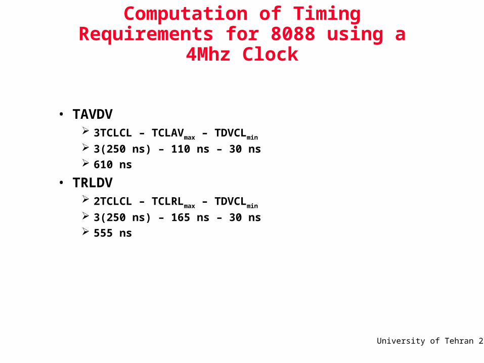
Computation of Timing Requirements for 8088 using a 4Mhz Clock
• TAVDV 3TCLCL – TCLAVmax – TDVCLmin
3(250 ns) – 110 ns – 30 ns 610 ns
• TRLDV 2TCLCL – TCLRLmax – TDVCLmin
3(250 ns) – 165 ns – 30 ns 555 ns
University of Tehran 26
8088 MINIMUM COMPLEXITY SYSTEM TIMING REQUIREMENTS
8088 8088-2 Symbol Parameter Min Max Min Max
Units
TCLCL CLK Cycle Period 200 500 125 500 ns
TCLCH CLK Low Time 118 68 ns
TDVCL Data Setup Time 30 20 ns
TCLAV Address Valid Delay 10 110 10 60 ns
TCLRL RD’ Active Delay 10 165 10 100 ns
TCLDV Data Valid Delay 10 110 10 60 ns
TCVCTX Control Inactive Delay 10 110 10 70 ns
TWHDX Data Hold Time after WR’ TCLCH – 30 TCLCH – 30 ns
TWLWH WR’ Width 2TCLCL – 60 2TCLCL – 40 ns
University of Tehran 27
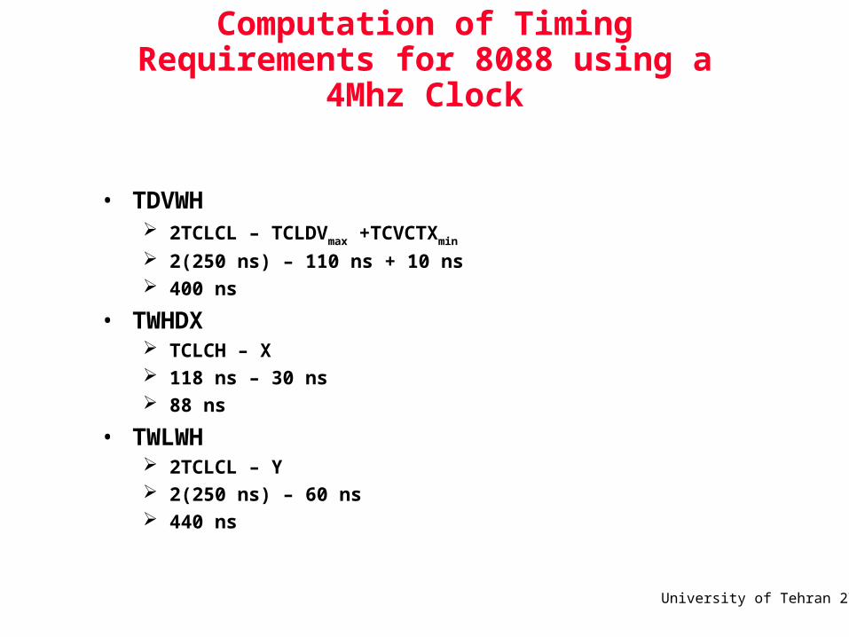
Computation of Timing Requirements for 8088 using a 4Mhz Clock
• TDVWH 2TCLCL – TCLDVmax +TCVCTXmin
2(250 ns) – 110 ns + 10 ns 400 ns
• TWHDX TCLCH – X 118 ns – 30 ns 88 ns
• TWLWH 2TCLCL – Y 2(250 ns) – 60 ns 440 ns
University of Tehran 28
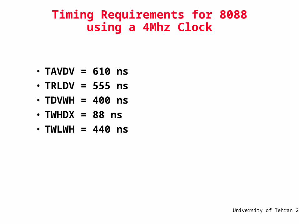
Timing Requirements for 8088 using a 4Mhz Clock
• TAVDV = 610 ns
• TRLDV = 555 ns
• TDVWH = 400 ns
• TWHDX = 88 ns
• TWLWH = 440 ns
University of Tehran 29
Can we interface a 6264 to the 8088 chip which uses a 4MHz clock?
University of Tehran 30
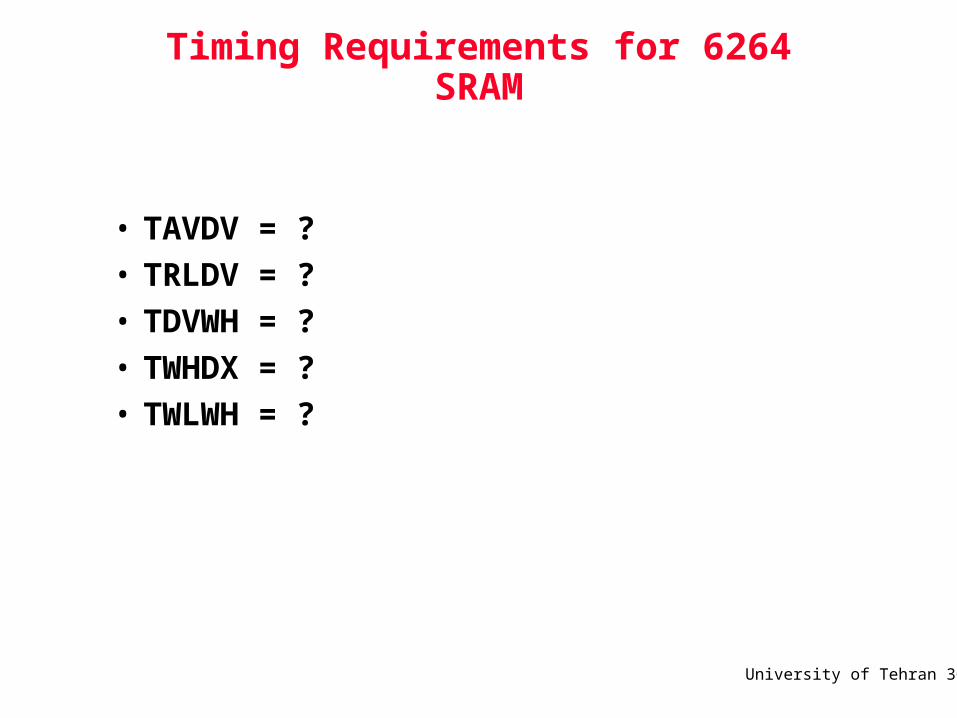
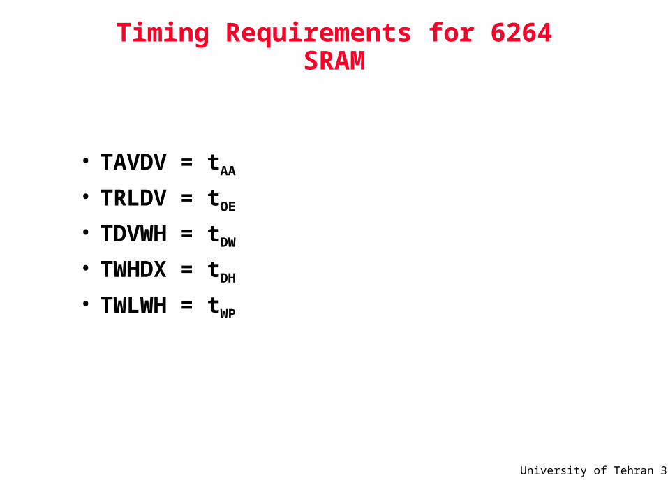
Timing Requirements for 6264 SRAM
• TAVDV = ?
• TRLDV = ?
• TDVWH = ?
• TWHDX = ?
• TWLWH = ?

University of Tehran 31
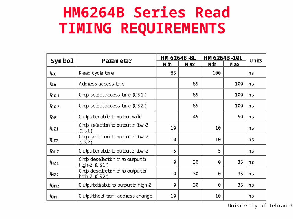
HM6264B Series Read TIMING REQUIREMENTS
HM6264B-8L HM6264B-10L Symbol Parameter Min Max Min Max
Units
tRC Read cycle time 85 100 ns
tAA Address access time 85 100 ns
tCO1 Chip select access time (CS1’) 85 100 ns
tCO2 Chip select access time (CS2’) 85 100 ns
tOE Output enable to output valid 45 50 ns
tLZ1 Chip selection to output in low-Z (CS1)
10 10 ns
tLZ2 Chip selection to output in low-Z (CS2)
10 10 ns
tOLZ Output enable to output in low-Z 5 5 ns
tHZ1 Chip deselection in to output in high-Z (CS1’)
0 30 0 35 ns
tHZ2 Chip deselection in to output in high-Z (CS2’)
0 30 0 35 ns
tOHZ Output disable to output in high-Z 0 30 0 35 ns
tOH Output hold from address change 10 10 ns
University of Tehran 32
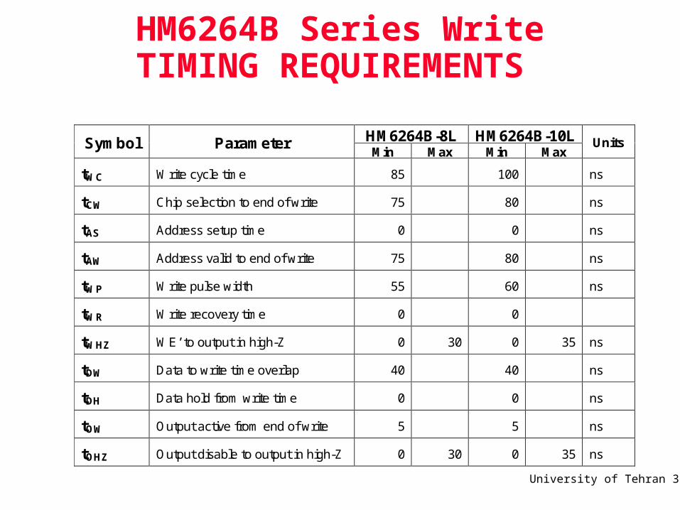
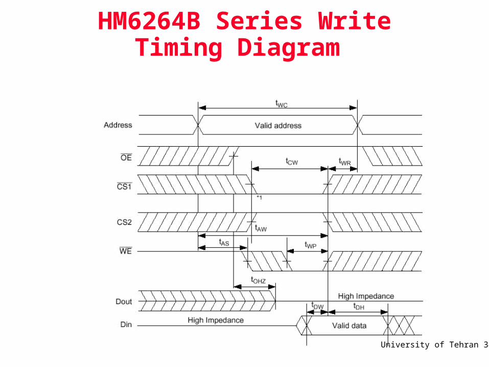
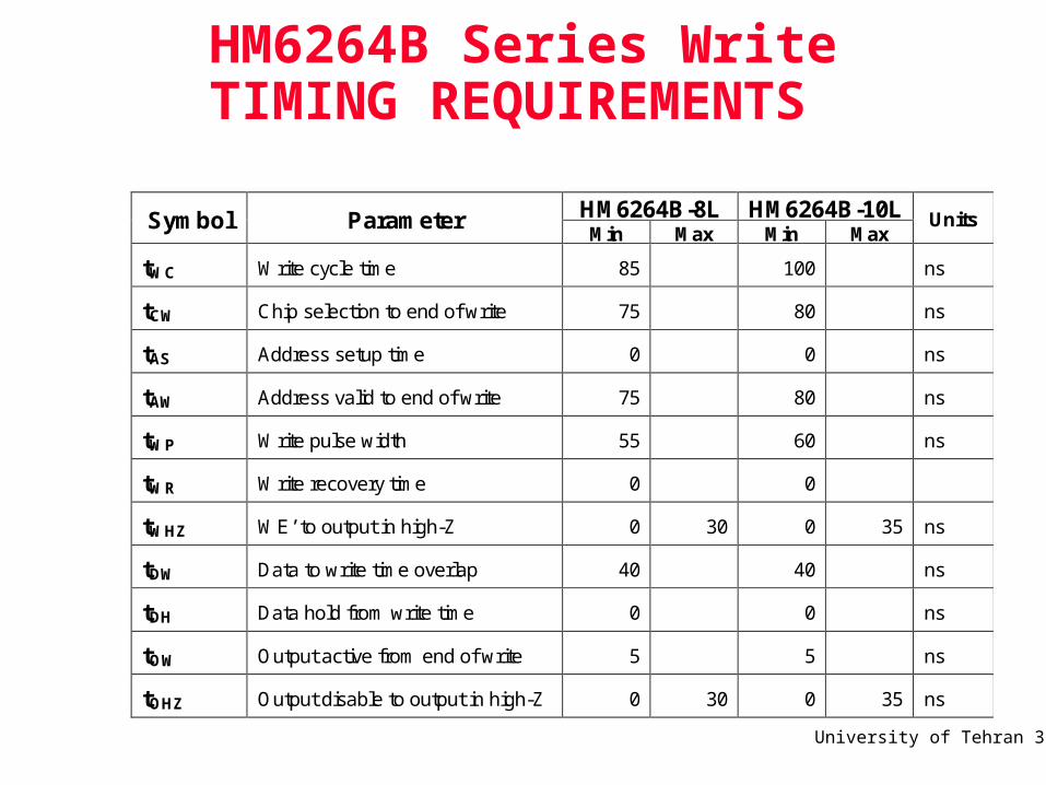
HM6264B Series Write TIMING REQUIREMENTS
HM6264B-8L HM6264B-10L Symbol Parameter Min Max Min Max
Units
tWC Write cycle time 85 100 ns
tCW Chip selection to end of write 75 80 ns
tAS Address setup time 0 0 ns
tAW Address valid to end of write 75 80 ns
tWP Write pulse width 55 60 ns
tWR Write recovery time 0 0
tWHZ WE’ to output in high-Z 0 30 0 35 ns
tDW Data to write time overlap 40 40 ns
tDH Data hold from write time 0 0 ns
tOW Output active from end of write 5 5 ns
tOHZ Output disable to output in high-Z 0 30 0 35 ns
University of Tehran 33
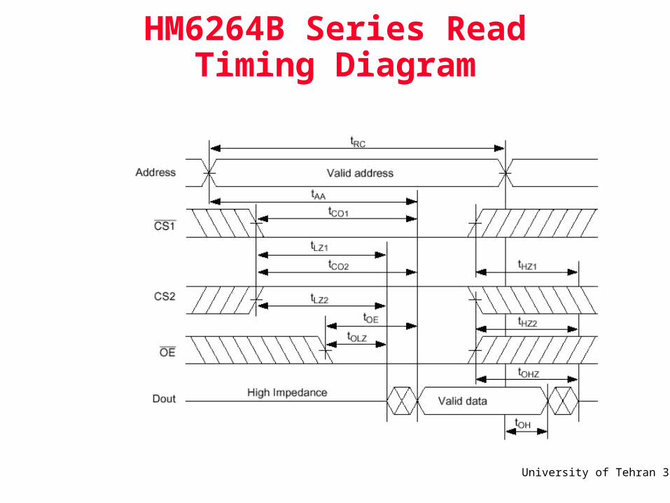
HM6264B Series Read Timing Diagram
University of Tehran 34
HM6264B Series Write Timing Diagram
University of Tehran 35
Timing Requirements for 6264 SRAM
• TAVDV = tAA
• TRLDV = tOE
• TDVWH = tDW
• TWHDX = tDH
• TWLWH = tWP
University of Tehran 36
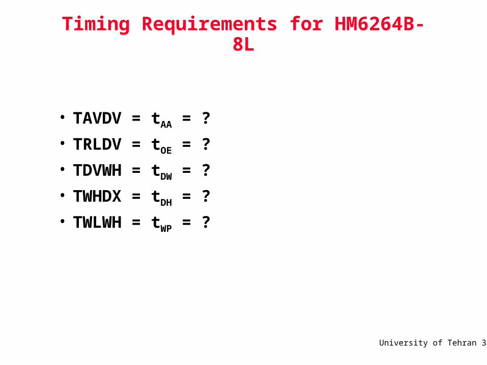
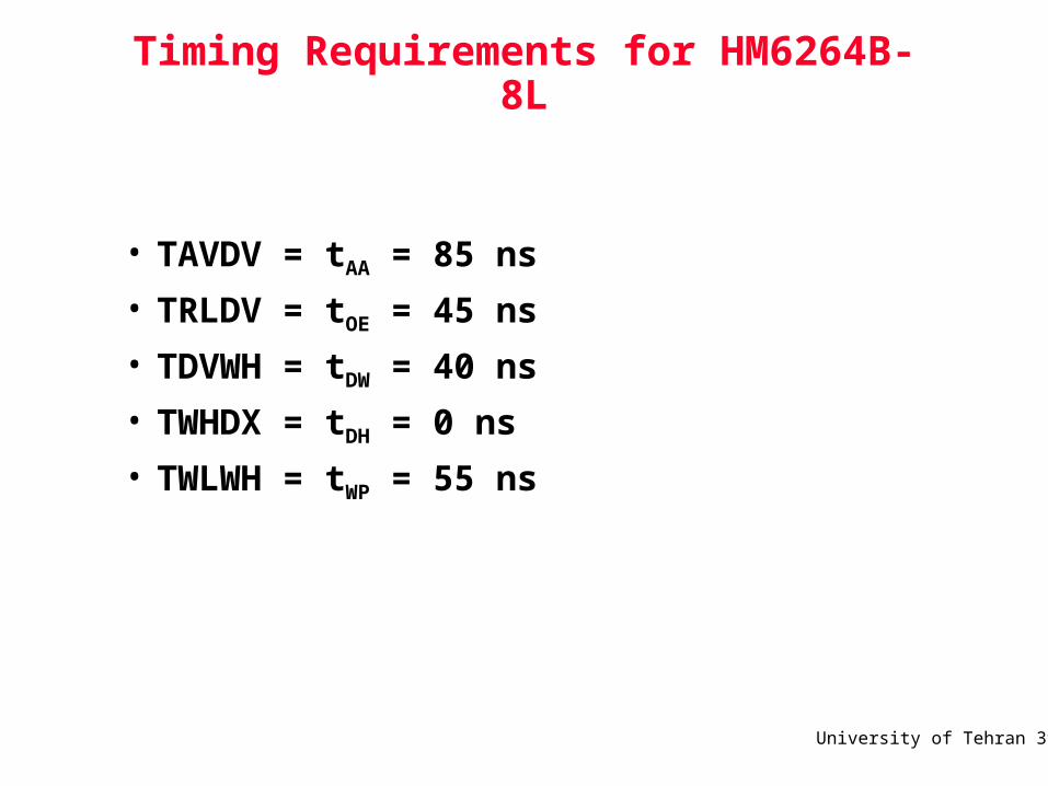
Timing Requirements for HM6264B-8L
• TAVDV = tAA = ?
• TRLDV = tOE = ?
• TDVWH = tDW = ?
• TWHDX = tDH = ?
• TWLWH = tWP = ?
University of Tehran 37
HM6264B Series Read TIMING REQUIREMENTS
HM6264B-8L HM6264B-10L Symbol Parameter Min Max Min Max
Units
tRC Read cycle time 85 100 ns
tAA Address access time 85 100 ns
tCO1 Chip select access time (CS1’) 85 100 ns
tCO2 Chip select access time (CS2’) 85 100 ns
tOE Output enable to output valid 45 50 ns
tLZ1 Chip selection to output in low-Z (CS1)
10 10 ns
tLZ2 Chip selection to output in low-Z (CS2)
10 10 ns
tOLZ Output enable to output in low-Z 5 5 ns
tHZ1 Chip deselection in to output in high-Z (CS1’)
0 30 0 35 ns
tHZ2 Chip deselection in to output in high-Z (CS2’)
0 30 0 35 ns
tOHZ Output disable to output in high-Z 0 30 0 35 ns
tOH Output hold from address change 10 10 ns
University of Tehran 38
HM6264B Series Write TIMING REQUIREMENTS
HM6264B-8L HM6264B-10L Symbol Parameter Min Max Min Max
Units
tWC Write cycle time 85 100 ns
tCW Chip selection to end of write 75 80 ns
tAS Address setup time 0 0 ns
tAW Address valid to end of write 75 80 ns
tWP Write pulse width 55 60 ns
tWR Write recovery time 0 0
tWHZ WE’ to output in high-Z 0 30 0 35 ns
tDW Data to write time overlap 40 40 ns
tDH Data hold from write time 0 0 ns
tOW Output active from end of write 5 5 ns
tOHZ Output disable to output in high-Z 0 30 0 35 ns
University of Tehran 39
Timing Requirements for HM6264B-8L
• TAVDV = tAA = 85 ns
• TRLDV = tOE = 45 ns
• TDVWH = tDW = 40 ns
• TWHDX = tDH = 0 ns
• TWLWH = tWP = 55 ns
University of Tehran 40
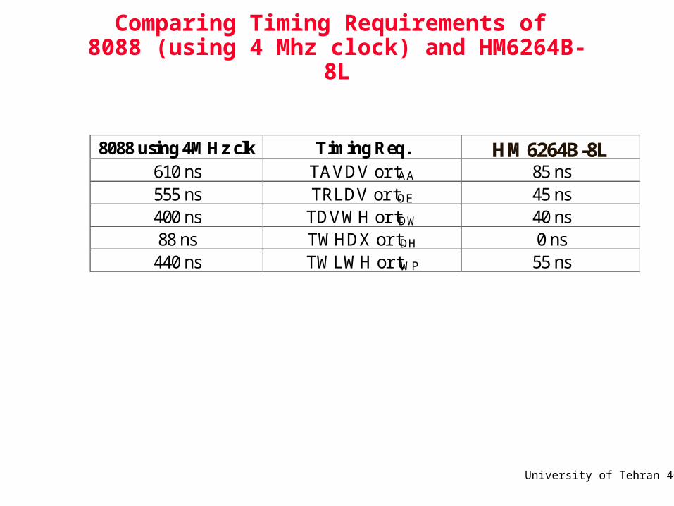
Comparing Timing Requirements of 8088 (using 4 Mhz clock) and HM6264B-8L
8088 using 4MHz clk Timing Req. HM6264B-8L 610 ns TAVDV or tAA 85 ns
555 ns TRLDV or tOE 45 ns 400 ns TDVWH or tDW 40 ns
88 ns TWHDX or tDH 0 ns
440 ns TWLWH or tWP 55 ns
University of Tehran 41
Can we interface a 2764 to the 8088 chip which uses a 4MHz clock?
University of Tehran 42
Timing Requirements for 2764 EPROM
• TAVDV = ?
• TRLDV = ?
• TDVWH = ?
• TWHDX = ?
• TWLWH = ?

University of Tehran 43
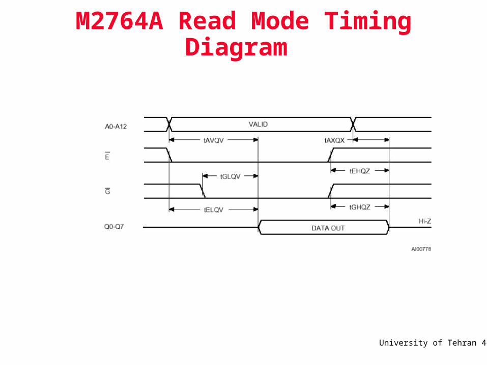
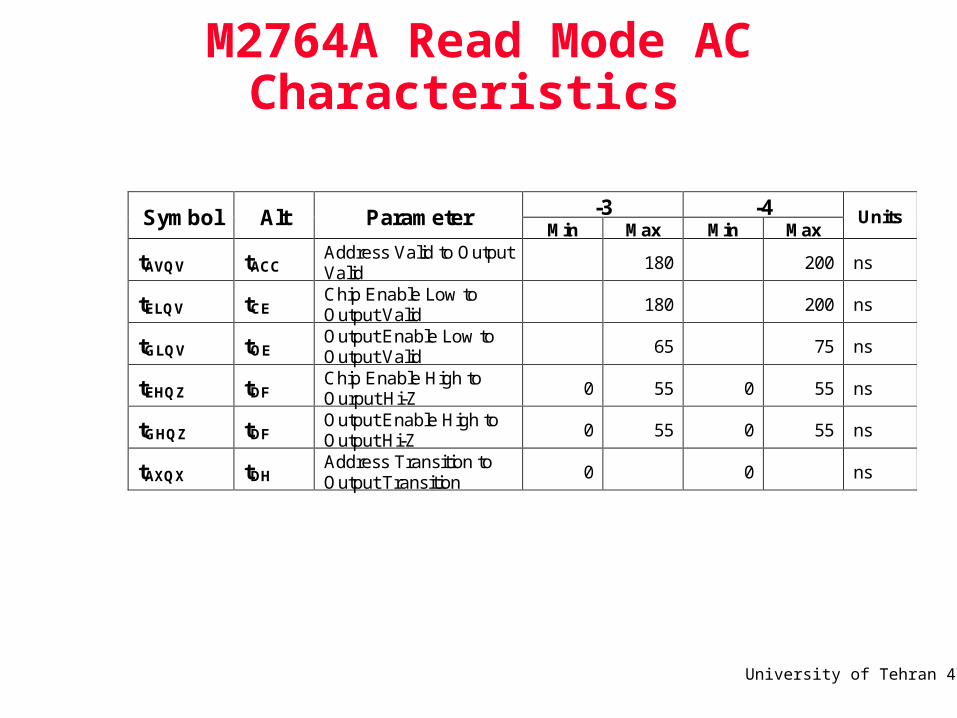
M2764A Read Mode AC Characteristics
-3 -4 Symbol Alt Parameter Min Max Min Max
Units
tAVQV tACC Address Valid to Output Valid
180 200 ns
tELQV tCE Chip Enable Low to Output Valid
180 200 ns
tGLQV tOE Output Enable Low to Output Valid
65 75 ns
tEHQZ tDF Chip Enable High to Ourput Hi-Z
0 55 0 55 ns
tGHQZ tDF Output Enable High to Output Hi-Z
0 55 0 55 ns
tAXQX tDH Address Transition to Output Transition
0 0 ns
University of Tehran 44
M2764A Read Mode Timing Diagram
University of Tehran 45
Timing Requirements for 2764 EPROM
• TAVDV = tAVQV
• TRLDV = tGLQV
• TDVWH = N/A
• TWHDX = N/A
• TWLWH = N/A
University of Tehran 46
Timing Requirements for 2764 EPROM
• TAVDV = tAVQV = ?
• TRLDV = tGLQV = ?
• TDVWH = N/A
• TWHDX = N/A
• TWLWH = N/A
University of Tehran 47
M2764A Read Mode AC Characteristics
-3 -4 Symbol Alt Parameter Min Max Min Max
Units
tAVQV tACC Address Valid to Output Valid
180 200 ns
tELQV tCE Chip Enable Low to Output Valid
180 200 ns
tGLQV tOE Output Enable Low to Output Valid
65 75 ns
tEHQZ tDF Chip Enable High to Ourput Hi-Z
0 55 0 55 ns
tGHQZ tDF Output Enable High to Output Hi-Z
0 55 0 55 ns
tAXQX tDH Address Transition to Output Transition
0 0 ns
University of Tehran 48
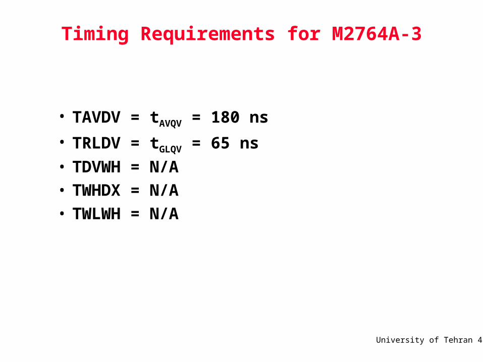
Timing Requirements for M2764A-3
• TAVDV = tAVQV = 180 ns
• TRLDV = tGLQV = 65 ns
• TDVWH = N/A
• TWHDX = N/A
• TWLWH = N/A
University of Tehran 49
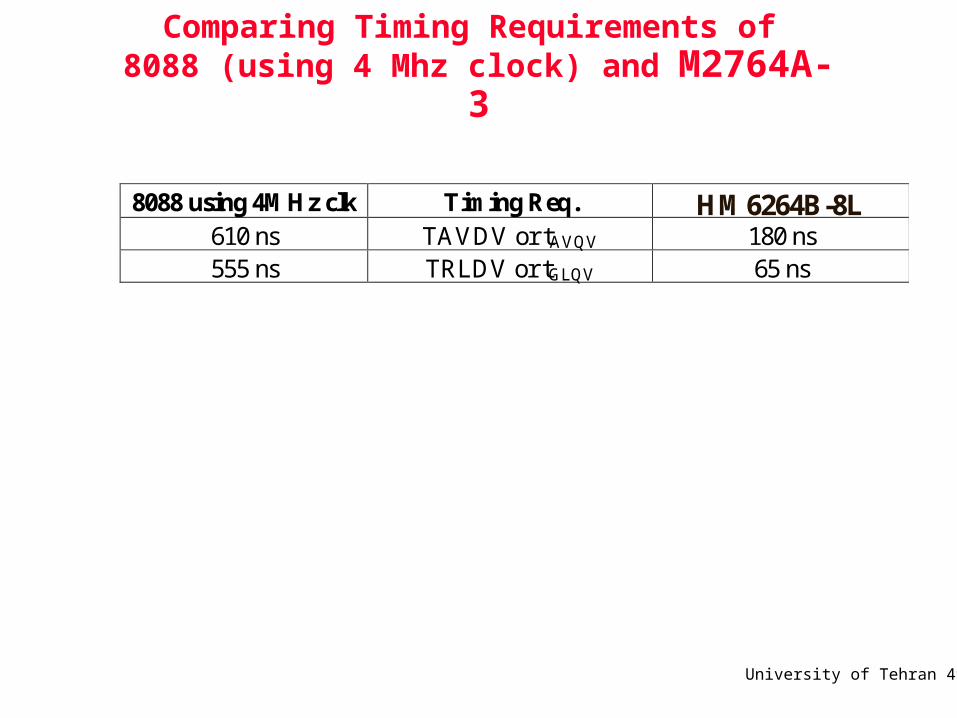
Comparing Timing Requirements of 8088 (using 4 Mhz clock) and M2764A-3
8088 using 4MHz clk Timing Req. HM6264B-8L 610 ns TAVDV or tAVQV 180 ns
555 ns TRLDV or tGLQV 65 ns

University of Tehran 50
What if we need to interface a “slow” memory to the 8088?
University of Tehran 51
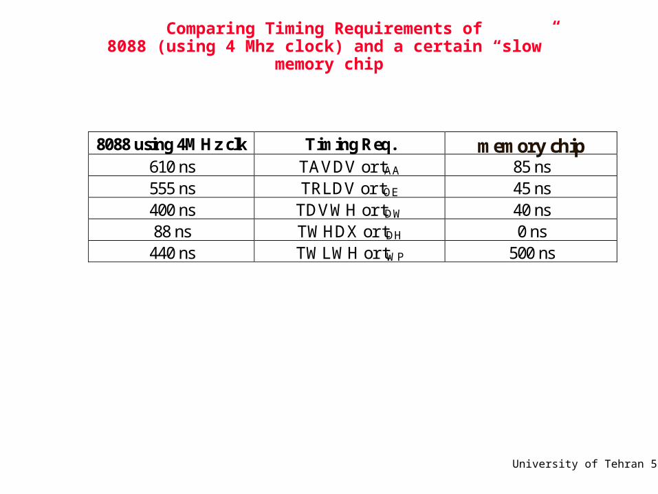
Comparing Timing Requirements of 8088 (using 4 Mhz clock) and a certain “slow” memory chip
8088 using 4MHz clk Timing Req. memory chip 610 ns TAVDV or tAA 85 ns
555 ns TRLDV or tOE 45 ns 400 ns TDVWH or tDW 40 ns
88 ns TWHDX or tDH 0 ns
440 ns TWLWH or tWP 500 ns

University of Tehran 52
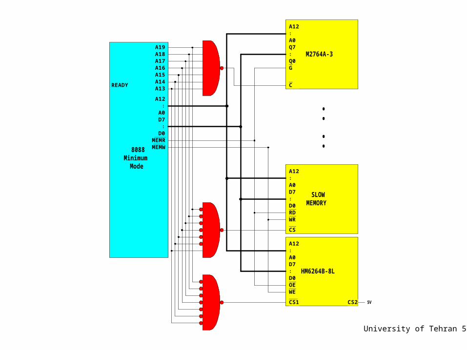
8088Minimum
Mode
A12
A0:
D7
D0:
MEMRMEMW
A13A14
HM6264B-8L
A12
A0:
D7
D0:
OEWE
CS1 CS2
SLOWMEMORY
A12
A0:
D7
D0:
RDWR
CS
M2764A-3
A12
A0:
Q7
Q0:
G
C
A15A16A17A18A19
::
5V
READY
University of Tehran 53
Recall:Write Pulse Width / Write-Time (TWLWH)
ALE
T1
CLOCK
T2 T3 T4
AD7 - AD0
A15 - A8
A19/S6 - A16/S3
DT/R __
IO/M __
_____
WR
DEN______
A19 - A0from 74LS373 to memory
A15 - A8
A19 - A16 S6 - S3
A19 - A0 from 74LS373
A7 - A0 D7 - D0 (to 74LS245)
D7 - D0from 74LS245 to memory
D7 - D0 (to memory)A7 - A0
TWLWH
2TCLCL
University of Tehran 54
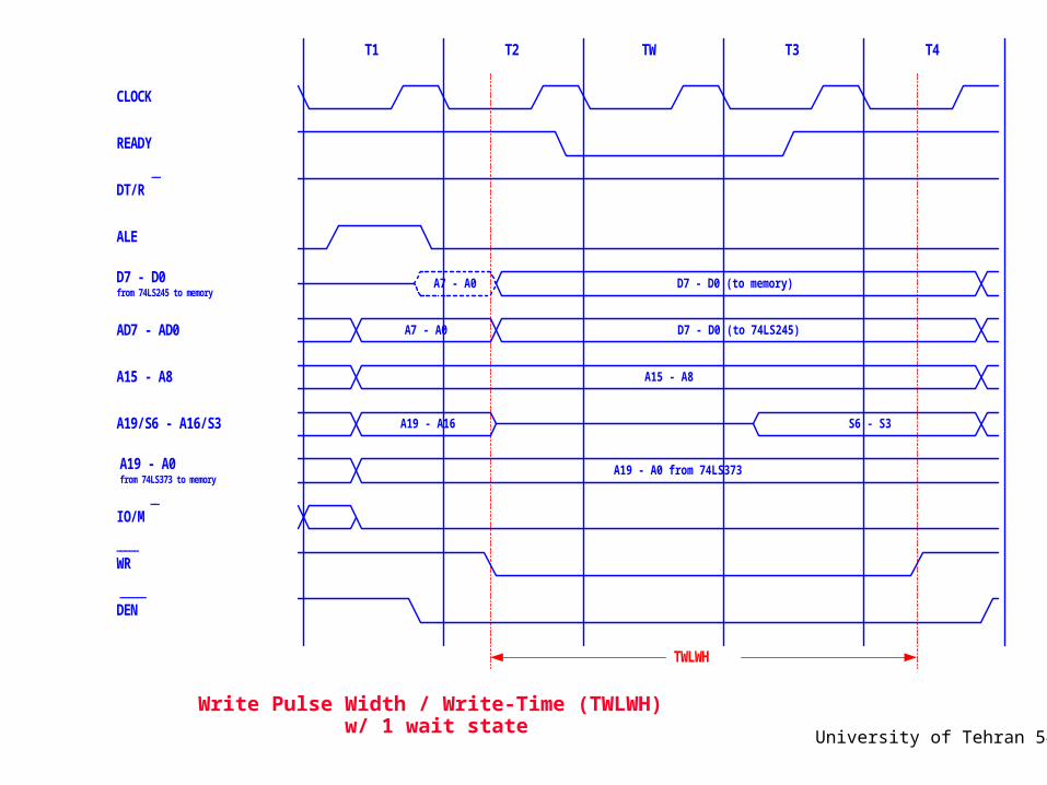
Write Pulse Width / Write-Time (TWLWH) w/ 1 wait state
ALE
T1
CLOCK
T2 T4
AD7 - AD0
A15 - A8
A19/S6 - A16/S3
READY
IO/M __
_____
WR
DEN______
A19 - A0from 74LS373 to memory
D7 - D0from 74LS245 to memory
TWLWH
A7 - A0 D7 - D0 (to memory)
A7 - A0 D7 - D0 (to 74LS245)
A15 - A8
A19 - A16 S6 - S3
A19 - A0 from 74LS373
DT/R __
TW T3
University of Tehran 55
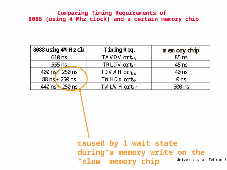
Comparing Timing Requirements of 8088 (using 4 Mhz clock) and a certain memory chip
8088 using 4MHz clk Timing Req. memory chip 610 ns TAVDV or tAA 85 ns
555 ns TRLDV or tOE 45 ns 400 ns + 250 ns TDVWH or tDW 40 ns
88 ns + 250 ns TWHDX or tDH 0 ns
440 ns + 250 ns TWLWH or tWP 500 ns
caused by 1 wait state during a memory write on the “slow” memory chip

University of Tehran 56
How do we produce a wait state?
• By turning the READY input of the 8088 microprocessor to LOW
University of Tehran 57
8088Minimum
Mode
A12
A0:
D7
D0:
MEMRMEMW
A13A14
HM6264B-8L
A12
A0:
D7
D0:
OEWE
CS1 CS2
SLOWMEMORY
A12
A0:
D7
D0:
RDWR
CS
M2764A-3
A12
A0:
Q7
Q0:
G
C
A15A16A17A18A19
::
5V
READY
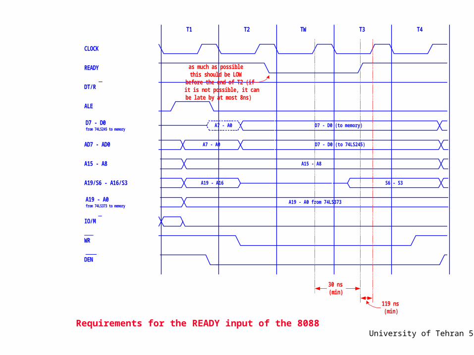
University of Tehran 58Requirements for the READY input of the 8088
ALE
T1
CLOCK
T2 T4
AD7 - AD0
A15 - A8
A19/S6 - A16/S3
READY
IO/M __
_____
WR
DEN______
A19 - A0from 74LS373 to memory
D7 - D0from 74LS245 to memory
30 ns(min)
A7 - A0 D7 - D0 (to memory)
A7 - A0 D7 - D0 (to 74LS245)
A15 - A8
A19 - A16 S6 - S3
A19 - A0 from 74LS373
DT/R __
TW T3
119 ns(min)
as much as possiblethis should be LOW
before the end of T2 (ifit is not possible, it canbe late by at most 8ns)
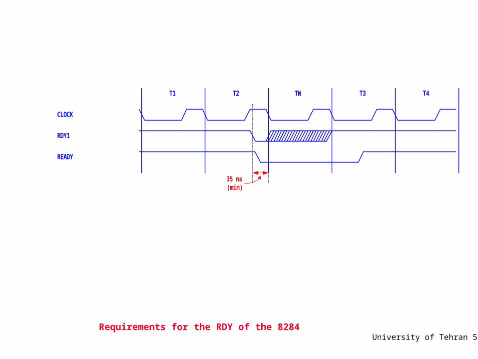
University of Tehran 59Requirements for the RDY of the 8284
T1
CLOCK
T2 T4
RDY1
35 ns(min)
TW T3
READY

University of Tehran 60
8088Minimum
Mode
A12
A0:
D7
D0:
MEMRMEMW
A13A14
HM6264B-8L
A12
A0:
D7
D0:
OEWE
CS1 CS2
SLOWMEMORY
A12
A0:
D7
D0:
RDWR
CS
M2764A-3
A12
A0:
Q7
Q0:
G
C
A15A16A17A18A19
::
5V
READY
University of Tehran 61
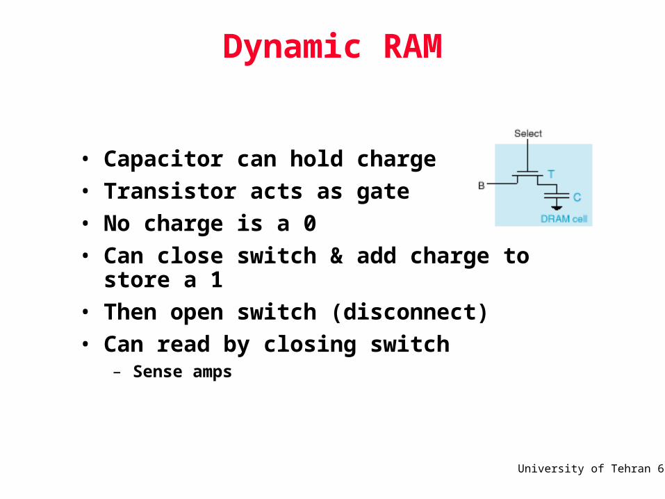
Dynamic RAM
• Capacitor can hold charge
• Transistor acts as gate
• No charge is a 0
• Can close switch & add charge to store a 1
• Then open switch (disconnect)
• Can read by closing switch– Sense amps
University of Tehran 62
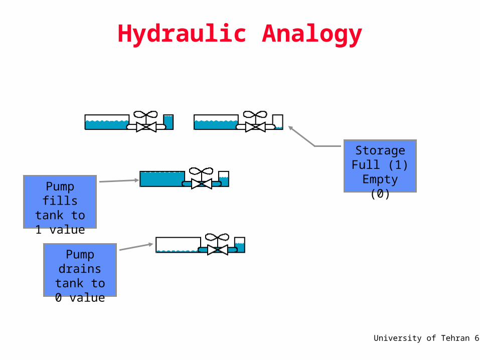
Hydraulic Analogy
StorageFull (1)
Empty (0)Pump fills tank to 1
value
Pump drains tank to 0 value
University of Tehran 63
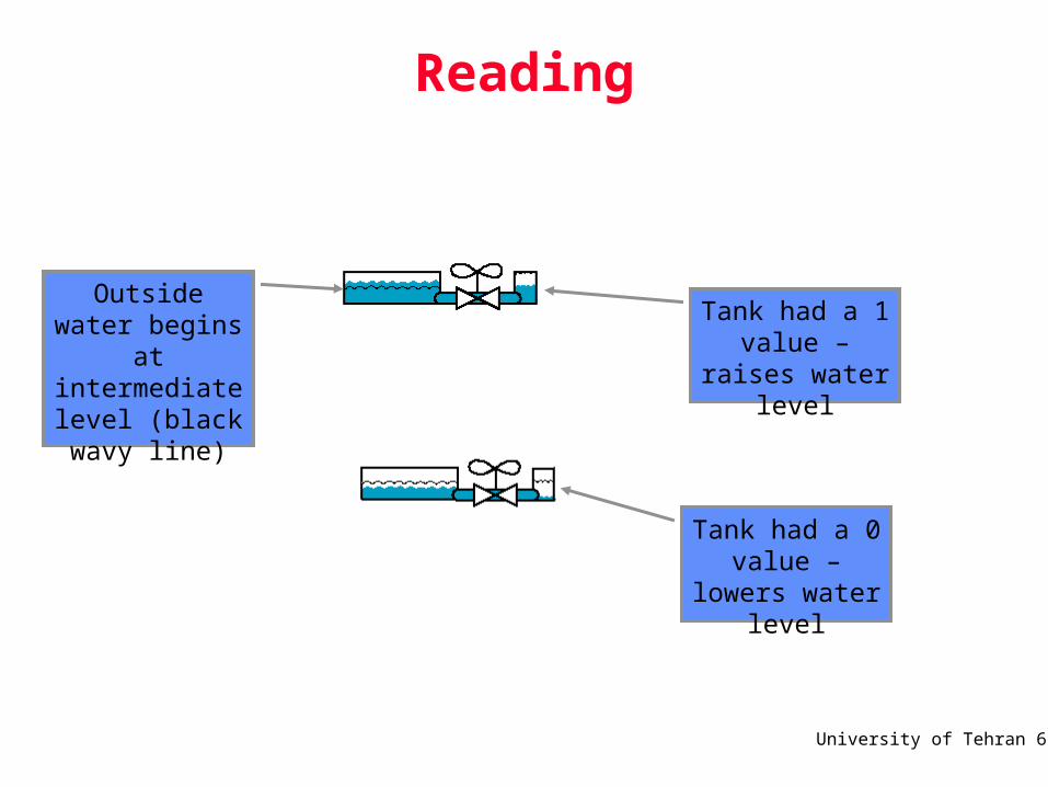
Reading
Tank had a 1 value – raises
water level
Outside water begins at
intermediate level (black wavy line)
Tank had a 0 value – lowers
water level
University of Tehran 64
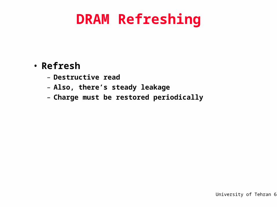
DRAM Refreshing
• Refresh– Destructive read
– Also, there’s steady leakage
– Charge must be restored periodically
University of Tehran 65
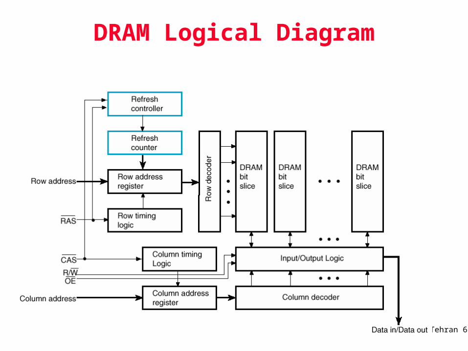
DRAM Logical Diagram
University of Tehran 66
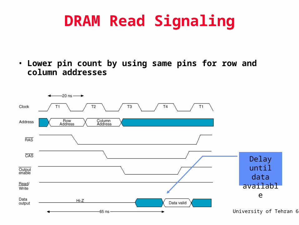
DRAM Read Signaling
• Lower pin count by using same pins for row and column addresses
Delay until data
available
University of Tehran 67
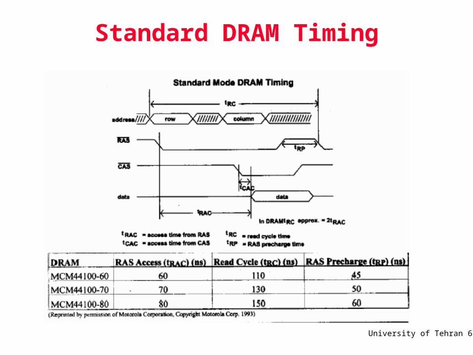
Standard DRAM Timing
University of Tehran 68
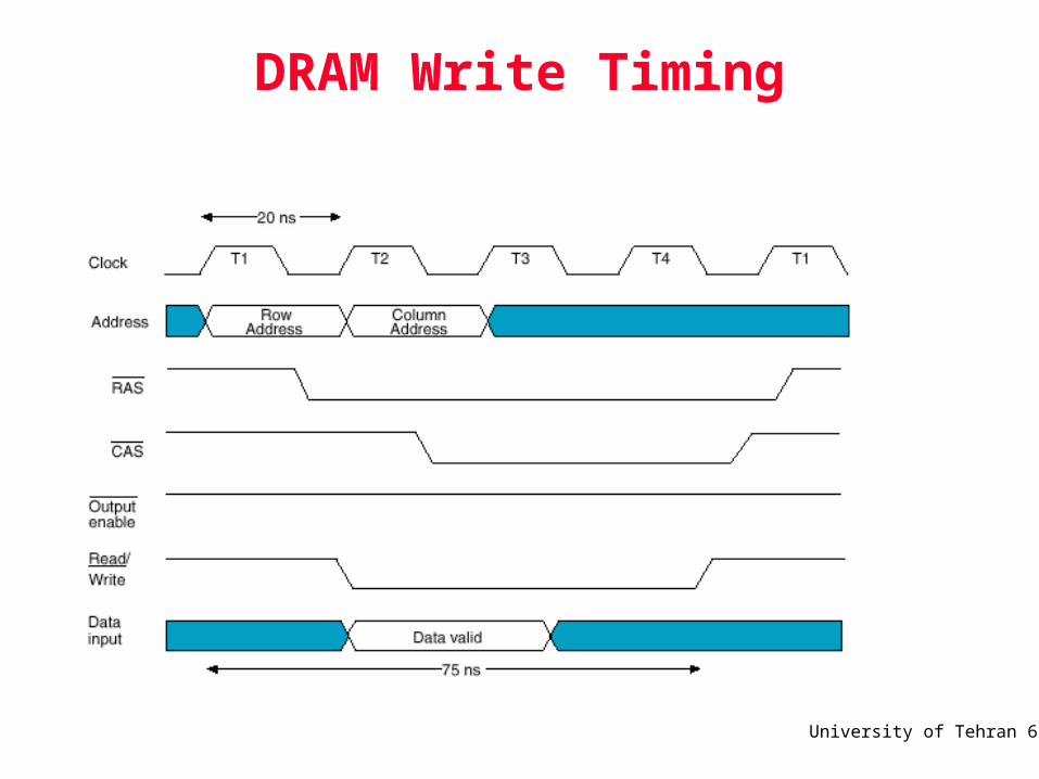
DRAM Write Timing
University of Tehran 69
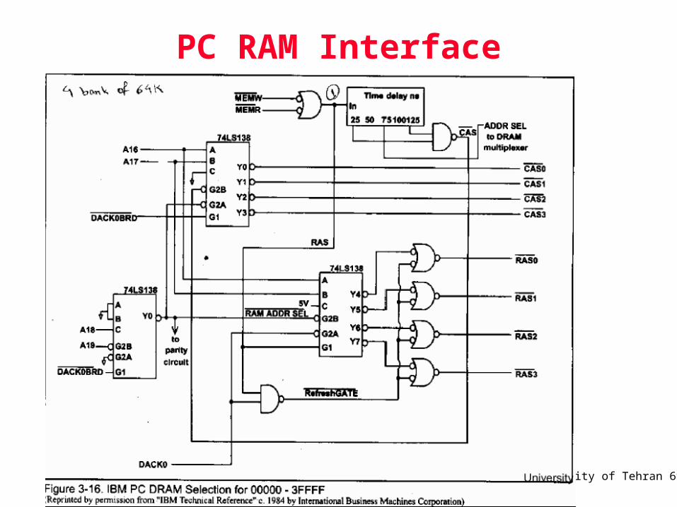
PC RAM Interface
University of Tehran 70
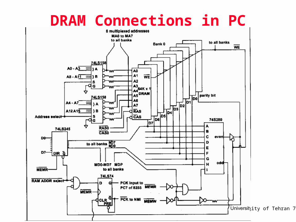
DRAM Connections in PC
University of Tehran 71
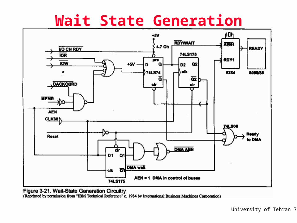
Wait State Generation
University of Tehran 72
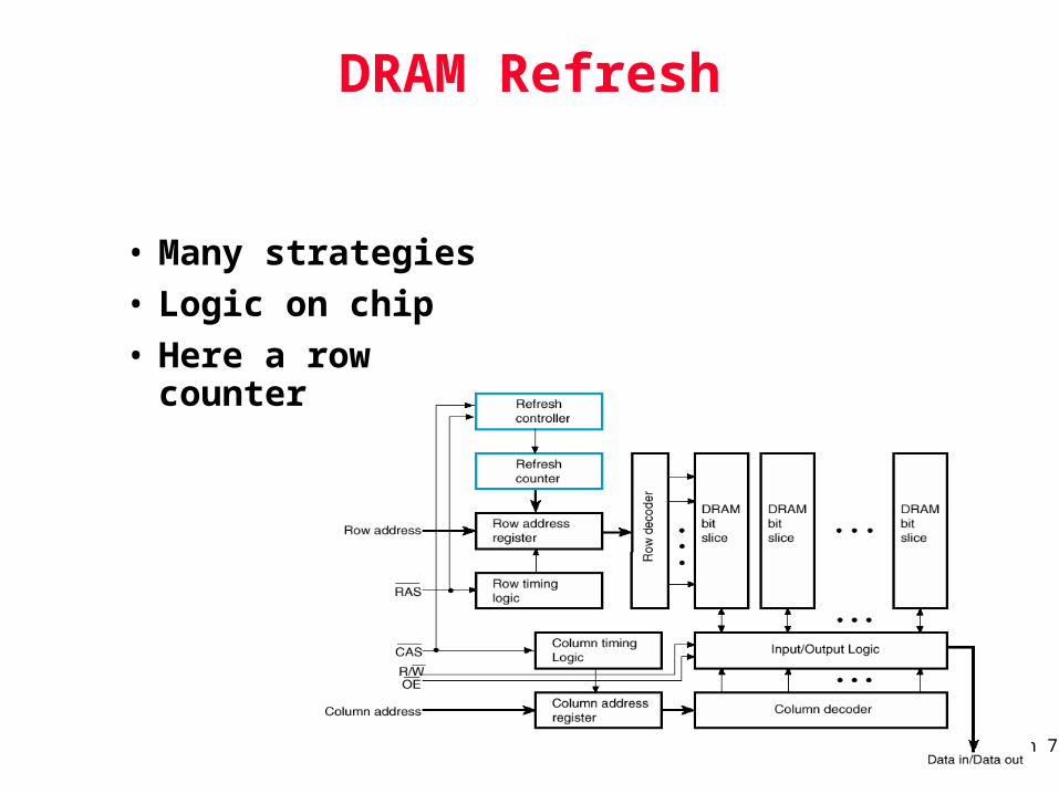
DRAM Refresh
• Many strategies
• Logic on chip
• Here a row counter

University of Tehran 73