Embed Size (px)
Citation preview
Document Number: 82187 www.vishay.comRev. 1.9, 19-Jun-08 211
IR Receiver Modules for Remote Control Systems
TSOP362..Vishay Semiconductors
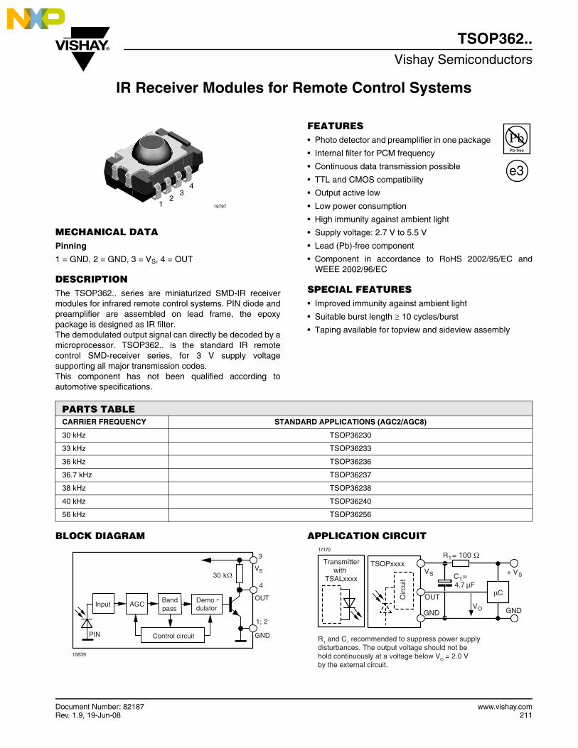
MECHANICAL DATAPinning
1 = GND, 2 = GND, 3 = VS, 4 = OUT
DESCRIPTIONThe TSOP362.. series are miniaturized SMD-IR receivermodules for infrared remote control systems. PIN diode andpreamplifier are assembled on lead frame, the epoxypackage is designed as IR filter.The demodulated output signal can directly be decoded by amicroprocessor. TSOP362.. is the standard IR remotecontrol SMD-receiver series, for 3 V supply voltagesupporting all major transmission codes.This component has not been qualified according toautomotive specifications.
FEATURES• Photo detector and preamplifier in one package
• Internal filter for PCM frequency
• Continuous data transmission possible
• TTL and CMOS compatibility
• Output active low
• Low power consumption
• High immunity against ambient light
• Supply voltage: 2.7 V to 5.5 V
• Lead (Pb)-free component
• Component in accordance to RoHS 2002/95/EC andWEEE 2002/96/EC
SPECIAL FEATURES• Improved immunity against ambient light
• Suitable burst length ≥ 10 cycles/burst
• Taping available for topview and sideview assembly
BLOCK DIAGRAM APPLICATION CIRCUIT
1679712
34
e3
PARTS TABLECARRIER FREQUENCY STANDARD APPLICATIONS (AGC2/AGC8)
30 kHz TSOP36230
33 kHz TSOP36233
36 kHz TSOP36236
36.7 kHz TSOP36237
38 kHz TSOP36238
40 kHz TSOP36240
56 kHz TSOP36256
30 kΩVS
OUTDemo -
GND
passAGCInput
PIN
Banddulator
Control circuit
3
4
1; 2
16839
C1=4.7 µF
TSOPxxxx
GND
Circ
uit
µC
R1= 100 Ω
+ VS
GND
Transmitterwith
TSALxxxxVS
R1 and C1 recommended to suppress power supplydisturbances. The output voltage should not behold continuously at a voltage below VO = 2.0 Vby the external circuit.
VO
17170
OUT
www.vishay.com Document Number: 82187212 Rev. 1.9, 19-Jun-08
TSOP362..Vishay Semiconductors IR Receiver Modules for
Remote Control Systems
Note(1) Stresses beyond those listed under “Absolute Maximum Ratings” may cause permanent damage to the device. This is a stress rating only
and functional operation of the device at these or any other conditions beyond those indicated in the operational sections of this specificationis not implied. Exposure to absolute maximum rating condtions for extended periods may affect the device reliability.
Note(1) Tamb = 25 °C, unless otherwise specified
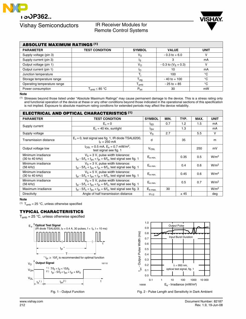
TYPICAL CHARACTERISTICSTamb = 25 °C, unless otherwise specified
Fig. 1 - Output Function Fig. 2 - Pulse Length and Sensitivity in Dark Ambient
ABSOLUTE MAXIMUM RATINGS (1)
PARAMETER TEST CONDITION SYMBOL VALUE UNIT
Supply voltage (pin 3) VS - 0.3 to + 6.0 V
Supply current (pin 3) IS 3 mA
Output voltage (pin 1) VO - 0.3 to (VS + 0.3) V
Output current (pin 1) IO 10 mA
Junction temperature Tj 100 °C
Storage temperature range Tstg - 40 to + 100 °C
Operating temperature range Tamb - 25 to + 85 °C
Power consumption Tamb ≤ 85 °C Ptot 30 mW
ELECTRICAL AND OPTICAL CHARACTERISTICS (1)
PARAMETER TEST CONDITION SYMBOL MIN. TYP. MAX. UNIT
Supply currentEv = 0 ISD 0.7 1.2 1.5 mA
Ev = 40 klx, sunlight ISH 1.3 mA
Supply voltage VS 2.7 5.5 V
Transmission distance Ev = 0, test signal see fig. 1, IR diode TSAL6200, IF = 250 mA d 35 m
Output voltage low IOSL = 0.5 mA, Ee = 0.7 mW/m2, test signal see fig. 1 VOSL 250 mV
Minimum irradiance (30 to 40 kHz)
VS = 3 V, pulse width tolerance: tpi - 5/fo < tpo < tpi + 6/fo, test signal see fig. 1 Ee min. 0.35 0.5 W/m2
Minimum irradiance(56 kHz)
VS = 3 V, pulse width tolerance: tpi - 5/fo < tpo < tpi + 6/fo, test signal see fig. 1 Ee min. 0.4 0.6 W/m2
Minimum irradiance(30 to 40 kHz)
VS = 5 V, pulse width tolerance: tpi - 5/fo < tpo < tpi + 6/fo, test signal see fig. 1 Ee min. 0.45 0.6 W/m2
Minimum irradiance(56 kHz)
VS = 5 V, pulse width tolerance: tpi - 5/fo < tpo < tpi + 6/fo, test signal see fig. 1 Ee min. 0.5 0.7 W/m2
Maximum irradiance tpi - 5/fo < tpo < tpi + 6/fo, test signal see fig. 3 Ee max. 30 W/m2
Directivity Angle of half transmission distance ϕ1/2 ± 45 deg
Ee
T
tpi *
t
* tpi 10/f0 is recommended for optimal function
VO
VOH
VOLt
16110
Optical Test Signal(IR diode TSAL6200, IF = 0.4 A, 30 pulses, f = f0, t = 10 ms)
Output Signal
td1 ) tpo2 )
1 ) 7/f0 < td < 15/f02 ) tpi - 5/f0 < tpo < tpi + 6/f0
0.0
0.1
0.2
0.3
0.4
0.5
0.6
0.7
0.8
0.9
1.0
0.1 1 10 100 1000 10 000
Ee - Irradiance (mW/m²) 16908
Input Burst Duration
= 950 nm, optical test signal, fig. 1
Output Pulse
t -
Out
put P
ulse
Wid
th (
ms)
po
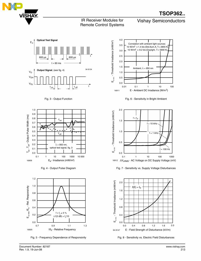
Document Number: 82187 www.vishay.comRev. 1.9, 19-Jun-08 213
TSOP362..IR Receiver Modules for Remote Control Systems
Vishay Semiconductors
Fig. 3 - Output Function
Fig. 4 - Output Pulse Diagram
Fig. 5 - Frequency Dependence of Responsivity
Fig. 6 - Sensitivity in Bright Ambient
Fig. 7 - Sensitivity vs. Supply Voltage Disturbances
Fig. 8 - Sensitivity vs. Electric Field Disturbances
Ee
t
VO
VOH
VOLt
600 µs 600 µs
t = 60 ms
t on t off
94 8134
Optical Test Signal
Output Signal, (see fig. 4)
T
,T-
Out
put P
ulse
Wid
th (
ms)
0.0
0.1
0.2
0.3
0.4
0.5
0.6
0.7
0.8
0.9
1.0
0.1 1 10 100 1000 10 000
Ee- Irradiance (mW/m²)16909
Toff
= 950 nm, optical test signal, fig. 3
Ton
onof
f
0.0
0.2
0.4
0.6
0.8
1.0
1.2
0.7 0.9 1.1 1.3
f/f0 - Relative Frequency16925
f = f0 ± 5 %
Δ f(3 dB) = f0/10E
/
E
- R
el. R
espo
nsiv
itye
min
.e
0.0
0.5
1.0
1.5
2.0
2.5
3.0
3.5
4.0
0.01 0.1 1 10 100
E - Ambient DC Irradiance (W/m2)16911
Correlation with ambient light sources:10 W/m2 1.4 klx (Std.illum.A, T= 2855 K)10 W/m2 8.2 klx (Daylight, T= 5900 K)
Ambient, = 950 nm
Ee
min
. - T
hres
hold
Irra
dian
ce (
mW
/m2 )
0.0
0.5
1.0
1.5
2.0
0.1 1 10 100 1000
VsRMS - AC Voltage on DC Supply Voltage (mV)16912
f = fo
f = 10 kHz
Ee
min
. - T
hres
hold
Irra
dian
ce (
mW
/m²)
f = 1 kHz
f = 100 Hz
Ee
min
. - T
hres
hold
Irra
dian
ce (
mW
/m²)
0.0 0.4 0.8 1.2 1.6
0.0
0.4
0.8
1.2
2.0
E - Field Strength of Disturbance (kV/m)
2.0
94 8147
1.6f(E) = f0
www.vishay.com Document Number: 82187214 Rev. 1.9, 19-Jun-08
TSOP362..Vishay Semiconductors IR Receiver Modules for
Remote Control Systems
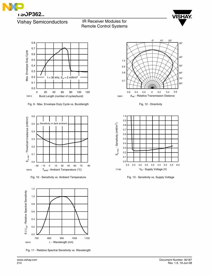
Fig. 9 - Max. Envelope Duty Cycle vs. Burstlength
Fig. 10 - Sensitivity vs. Ambient Temperature
Fig. 11 - Relative Spectral Sensitivity vs. Wavelength
Fig. 12 - Directivity
Fig. 13 - Sensitivity vs. Supply Voltage
0.0
0.1
0.2
0.3
0.4
0.5
0.6
0.7
0.8
0 20 40 60 80 100 120
Burst Length (number of cycles/burst)16913
f = 38 kHz, Ee = 2 mW/m2
Max
. Env
elop
e D
uty
Cyc
le
0.0
0.1
0.2
0.3
0.4
0.5
0.6
- 30 - 15 0 15 30 45 60 75 90
Tamb - Ambient Temperature (°C)16918
Sensitivity in dark ambient
E-
Thr
esho
ld Ir
radi
ance
(m
W/m
²)e
min
.
0.0
0.2
0.4
0.6
0.8
1.0
1.2
750 850 950 1050 1150
λ - Wavelength (nm)16919
S(
)-
Rel
ativ
eS
pect
ralS
ensi
tivity
λre
l
16801
0.4 0.2 0 0.2 0.4 0.60.6
0.9
0°30°
10° 20°
40°
50°
60°
70°
80°
1.0
0.8
0.7
drel - Relative Transmission Distance
0.0
0.1
0.2
0.3
0.4
0.5
0.6
0.7
0.8
0.9
1.0
2.0 2.5 3.0 3.5 4.0 4.5 5.0 5.5 6.0
VS - Supply Voltage (V)17185
E
-
Sen
sitiv
ity (
mW
/m )
2
e m
in.
Document Number: 82187 www.vishay.comRev. 1.9, 19-Jun-08 215
TSOP362..IR Receiver Modules for Remote Control Systems
Vishay Semiconductors
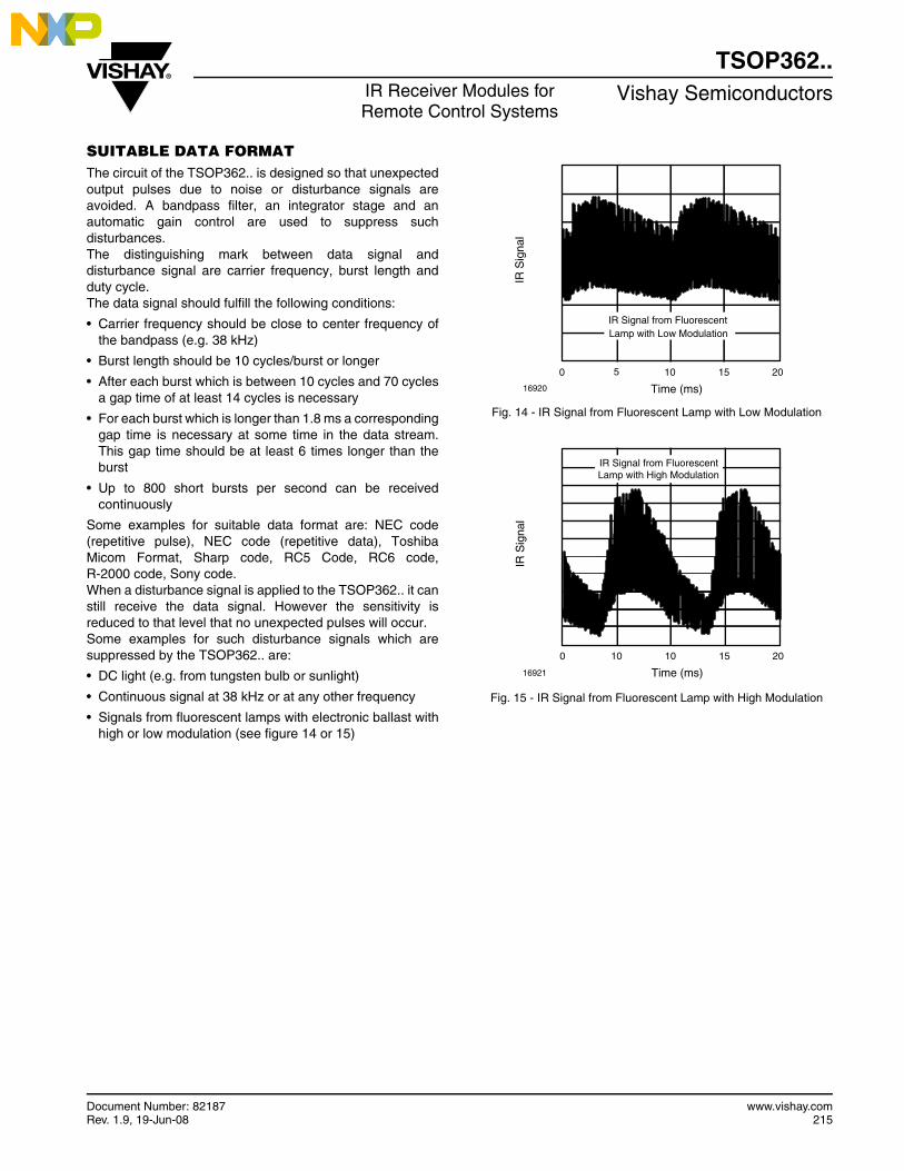
SUITABLE DATA FORMATThe circuit of the TSOP362.. is designed so that unexpectedoutput pulses due to noise or disturbance signals areavoided. A bandpass filter, an integrator stage and anautomatic gain control are used to suppress suchdisturbances.The distinguishing mark between data signal anddisturbance signal are carrier frequency, burst length andduty cycle.The data signal should fulfill the following conditions:
• Carrier frequency should be close to center frequency ofthe bandpass (e.g. 38 kHz)
• Burst length should be 10 cycles/burst or longer
• After each burst which is between 10 cycles and 70 cyclesa gap time of at least 14 cycles is necessary
• For each burst which is longer than 1.8 ms a correspondinggap time is necessary at some time in the data stream.This gap time should be at least 6 times longer than theburst
• Up to 800 short bursts per second can be receivedcontinuously
Some examples for suitable data format are: NEC code(repetitive pulse), NEC code (repetitive data), ToshibaMicom Format, Sharp code, RC5 Code, RC6 code,R-2000 code, Sony code.When a disturbance signal is applied to the TSOP362.. it canstill receive the data signal. However the sensitivity isreduced to that level that no unexpected pulses will occur.Some examples for such disturbance signals which aresuppressed by the TSOP362.. are:
• DC light (e.g. from tungsten bulb or sunlight)
• Continuous signal at 38 kHz or at any other frequency
• Signals from fluorescent lamps with electronic ballast withhigh or low modulation (see figure 14 or 15)
Fig. 14 - IR Signal from Fluorescent Lamp with Low Modulation
Fig. 15 - IR Signal from Fluorescent Lamp with High Modulation
0 10 15 20
Time (ms)16920
IR S
igna
l
IR Signal from FluorescentLamp with Low Modulation
5
0 10 15 20
Time (ms)16921
IR S
igna
l
IR Signal from FluorescentLamp with High Modulation
10
www.vishay.com Document Number: 82187216 Rev. 1.9, 19-Jun-08
TSOP362..Vishay Semiconductors IR Receiver Modules for
Remote Control Systems
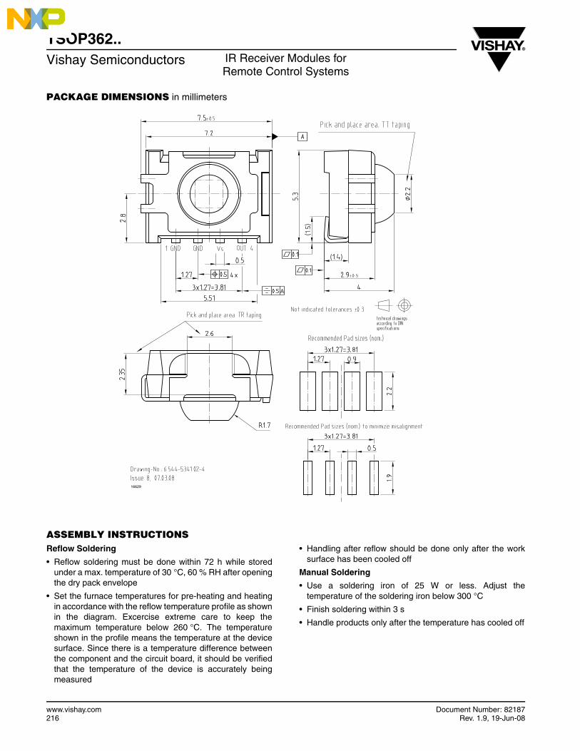
PACKAGE DIMENSIONS in millimeters
ASSEMBLY INSTRUCTIONSReflow Soldering
• Reflow soldering must be done within 72 h while storedunder a max. temperature of 30 °C, 60 % RH after openingthe dry pack envelope
• Set the furnace temperatures for pre-heating and heatingin accordance with the reflow temperature profile as shownin the diagram. Excercise extreme care to keep themaximum temperature below 260 °C. The temperatureshown in the profile means the temperature at the devicesurface. Since there is a temperature difference betweenthe component and the circuit board, it should be verifiedthat the temperature of the device is accurately beingmeasured
• Handling after reflow should be done only after the worksurface has been cooled off
Manual Soldering
• Use a soldering iron of 25 W or less. Adjust thetemperature of the soldering iron below 300 °C
• Finish soldering within 3 s
• Handle products only after the temperature has cooled off
16629
Document Number: 82187 www.vishay.comRev. 1.9, 19-Jun-08 217
TSOP362..IR Receiver Modules for Remote Control Systems
Vishay Semiconductors
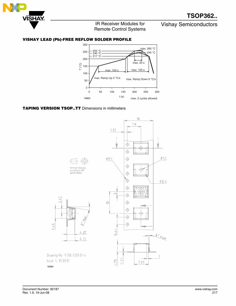
VISHAY LEAD (Pb)-FREE REFLOW SOLDER PROFILE
TAPING VERSION TSOP..TT Dimensions in millimeters
0
50
100
150
200
250
300
0 50 100 150 200 250 300
t (s)
T (
°C)
255 °C240 °C 245 °C
max. 260 °C
max. 120 s max. 100 s
217 °C
max. 20 s
max. Ramp Up 3 °C/s max. Ramp Down 6 °C/s
max. 2 cycles allowed19800
16584
www.vishay.com Document Number: 82187218 Rev. 1.9, 19-Jun-08
TSOP362..Vishay Semiconductors IR Receiver Modules for
Remote Control Systems
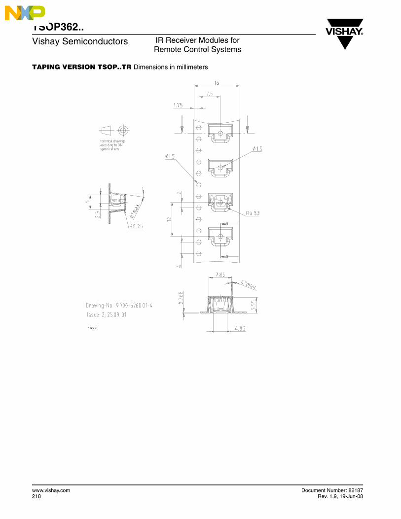
TAPING VERSION TSOP..TR Dimensions in millimeters
16585
Document Number: 82187 www.vishay.comRev. 1.9, 19-Jun-08 219
TSOP362..IR Receiver Modules for Remote Control Systems
Vishay Semiconductors
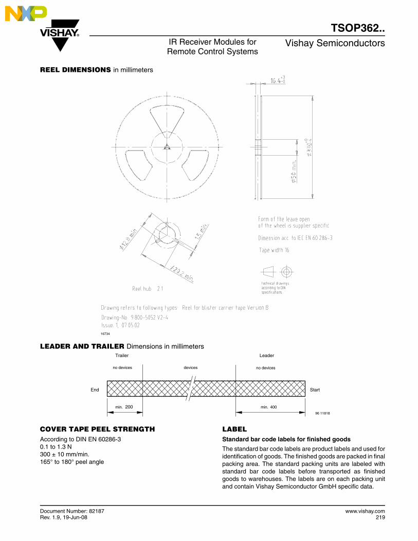
REEL DIMENSIONS in millimeters
LEADER AND TRAILER Dimensions in millimeters
COVER TAPE PEEL STRENGTHAccording to DIN EN 60286-30.1 to 1.3 N300 ± 10 mm/min.165° to 180° peel angle
LABELStandard bar code labels for finished goods
The standard bar code labels are product labels and used foridentification of goods. The finished goods are packed in finalpacking area. The standard packing units are labeled withstandard bar code labels before transported as finishedgoods to warehouses. The labels are on each packing unitand contain Vishay Semiconductor GmbH specific data.
16734
Trailer Leader
no devices
min. 200 min. 400
StartEnd
devices
96 11818
no devices
www.vishay.com Document Number: 82187220 Rev. 1.9, 19-Jun-08
TSOP362..Vishay Semiconductors IR Receiver Modules for
Remote Control Systems
DRY PACKINGThe reel is packed in an anti-humidity bag to protect thedevices from absorbing moisture during transportation andstorage.
FINAL PACKINGThe sealed reel is packed into a cardboard box. A secondarycardboard box is used for shipping purposes.
RECOMMENDED METHOD OF STORAGEDry box storage is recommended as soon as the aluminumbag has been opened to prevent moisture absorption. Thefollowing conditions should be observed, if dry boxes are notavailable:
• Storage temperature 10 °C to 30 °C
• Storage humidity ≤ 60 % RH max.
After more than 72 h under these conditions moisturecontent will be too high for reflow soldering.In case of moisture absorption, the devices will recover to theformer condition by drying under the following condition:192 h at 40 °C + 5 °C/- 0 °C and < 5 % RH (dry air/nitrogen)or 96 h at 60 °C + 5 °C and < 5 % RH for all device containers or 24 h at 125 °C + 5 °C not suitable for reel or tubes.An EIA JEDEC standard JESD22-A112 level 4 label isincluded on all dry bags.
Example of JESD22-A112 level 4 label
VISHAY SEMICONDUCTOR GMBH STANDARD BAR CODE PRODUCT LABEL (Finished Goods)PLAIN WRITING ABBREVIATION LENGTH
Item-description - 18
Item-number INO 8
Selection-code SEL 3
LOT-/serial-number BATCH 10
Data-code COD 3 (YWW)
Plant-code PTC 2
Quantity QTY 8
Accepted by ACC -
Packed by PCK -
Mixed code indicator MIXED CODE -
Origin xxxxxxx+ Company logo
LONG BAR CODE TOP TYPE LENGTH
Item-number N 8
Plant-code N 2
Sequence-number X 3
Quantity N 8
Total length - 21
SHORT BAR CODE BOTTOM TYPE LENGTH
Selection-code X 3
Data-code N 3
Batch-number X 10
Filter - 1
Total length - 17
Aluminum bag
Label
Reel
15973
16943
Document Number: 82187 www.vishay.comRev. 1.9, 19-Jun-08 221
TSOP362..IR Receiver Modules for Remote Control Systems
Vishay Semiconductors
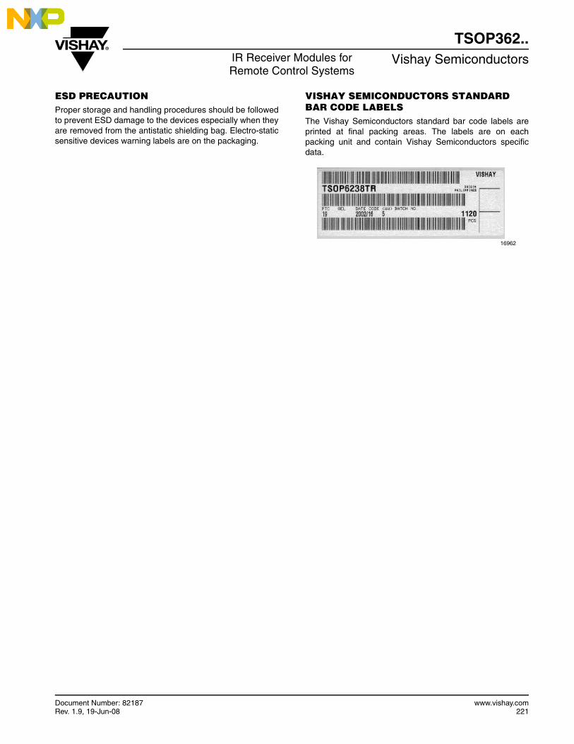
ESD PRECAUTIONProper storage and handling procedures should be followedto prevent ESD damage to the devices especially when theyare removed from the antistatic shielding bag. Electro-staticsensitive devices warning labels are on the packaging.
VISHAY SEMICONDUCTORS STANDARDBAR CODE LABELSThe Vishay Semiconductors standard bar code labels areprinted at final packing areas. The labels are on eachpacking unit and contain Vishay Semiconductors specificdata.
16962
www.vishay.com Document Number: 82187222 Rev. 1.9, 19-Jun-08
TSOP362..Vishay Semiconductors IR Receiver Modules for
Remote Control Systems
OZONE DEPLETING SUBSTANCES POLICY STATEMENTIt is the policy of Vishay Semiconductor GmbH to
1. Meet all present and future national and international statutory requirements.2. Regularly and continuously improve the performance of our products, processes, distribution and operating systems with
respect to their impact on the health and safety of our employees and the public, as well as their impact on the environment.
It is particular concern to control or eliminate releases of those substances into the atmosphere which are known as ozonedepleting substances (ODSs).
The Montreal Protocol (1987) and its London Amendments (1990) intend to severely restrict the use of ODSs and forbid their usewithin the next ten years. Various national and international initiatives are pressing for an earlier ban on these substances.
Vishay Semiconductor GmbH has been able to use its policy of continuous improvements to eliminate the use of ODSs listed inthe following documents.
1. Annex A, B and list of transitional substances of the Montreal Protocol and the London Amendments respectively.2. Class I and II ozone depleting substances in the Clean Air Act Amendments of 1990 by the Environmental Protection Agency
(EPA) in the USA.3. Council Decision 88/540/EEC and 91/690/EEC Annex A, B and C (transitional substances) respectively.
Vishay Semiconductor GmbH can certify that our semiconductors are not manufactured with ozone depleting substances and donot contain such substances.
We reserve the right to make changes to improve technical design and may do so without further notice.
Parameters can vary in different applications. All operating parameters must be validated for each customer application by the customer. Should the buyer use Vishay Semiconductors products for any unintended or unauthorized application, the buyer shall
indemnify Vishay Semiconductors against all claims, costs, damages, and expenses, arising out of, directly or indirectly, any claim of personal damage, injury or death associated with such unintended or unauthorized use.
Vishay Semiconductor GmbH, P.O.B. 3535, D-74025 Heilbronn, Germany
Document Number: 91000 www.vishay.comRevision: 18-Jul-08 1
Disclaimer
Legal Disclaimer NoticeVishay
All product specifications and data are subject to change without notice.
Vishay Intertechnology, Inc., its affiliates, agents, and employees, and all persons acting on its or their behalf(collectively, “Vishay”), disclaim any and all liability for any errors, inaccuracies or incompleteness contained hereinor in any other disclosure relating to any product.
Vishay disclaims any and all liability arising out of the use or application of any product described herein or of anyinformation provided herein to the maximum extent permitted by law. The product specifications do not expand orotherwise modify Vishay’s terms and conditions of purchase, including but not limited to the warranty expressedtherein, which apply to these products.
No license, express or implied, by estoppel or otherwise, to any intellectual property rights is granted by thisdocument or by any conduct of Vishay.
The products shown herein are not designed for use in medical, life-saving, or life-sustaining applications unlessotherwise expressly indicated. Customers using or selling Vishay products not expressly indicated for use in suchapplications do so entirely at their own risk and agree to fully indemnify Vishay for any damages arising or resultingfrom such use or sale. Please contact authorized Vishay personnel to obtain written terms and conditions regardingproducts designed for such applications.
Product names and markings noted herein may be trademarks of their respective owners.