Embed Size (px)
Citation preview

VISHAY TSOP5700Vishay Semiconductors
IR Receiver for High Data Rate PCM at 455 kHz
Description
167971234
The TSOP5700 is a miniaturized SMD IR receiver forinfrared remote control and IR data transmission. PINdiode and preamplifier are assembled on lead frame,the epoxy package is designed as IR filter.The demodulated output signal can directly bedecoded by a microprocessor. The main benefit is theoperation with high data rates and long distances.
Features • Photo detector and preamplifier in one package • Internal Bandfilter for PCM frequency
• Internal shielding against electrical field
disturbance• TTL and CMOS compatibility • Output active low • Small size package
Special Features • Data rate 20 kbit/s • Supply voltage 2.7 - 5.5 V
• Short settling time after power on • High envelope duty cycle can be received • Enhanced immunity against disturbance from
energy saving lamps • Taping available for topview and sideview
assembly
Mechanical DataPinning:1 = GND, 2 = NC, 3 = OUT, 4 = VS
Block DiagramApplication Circuit
10 kΩ3
1
VS
OUTDemo-
GND
PassAGCInput
PIN
Banddulator
Control Circuit
416840
C1 =4.7 µF
TSOPxxxx
OUT
GND
Circuit
µC
R1 = 47 Ω
+VS
GND
Transmitterwith
TSHFxxxxVS
R1 + C1 recommended to suppress power supply
disturbances.
VO
R2 >=1 kΩ
R2 optional for improved pulse forming.
16843
Document Number 82166
Rev. 5, 14-Aug-03
www.vishay.com
1

VISHAYTSOP5700Vishay Semiconductors
Absolute Maximum RatingsTamb = 25 °C, unless otherwise specified
Electrical and Optical CharacteristicsTamb = 25 °C, unless otherwise specified
Parameter Test condition Symbol Value Unit
Supply Voltage Pin 4 VS - 0.3 to + 6.0 V
Voltage at output to supply Pin 3 VS - VO - 0.3 to (VS + 0.3)
V
Supply Current Pin 4 IS 5 mA
Output Voltage Pin 3 VO - 0.3 to + 6.0 V
Output Current Pin 3 IO 15 mA
Junction Temperature Tj 100 °C
Storage Temperature Range Tstg - 40 to + 85 °C
Operating Temperature Range Tamb - 25 to + 85 °C
Power Consumption Tamb ≤ 85 °C Ptot 50 mW
Parameter Test condition Symbol Min Typ. Max Unit
Supply Current (Pin 4) Dark ambient ISD 2.0 2.7 mA
Ev = 40 klx, sunlight ISH 2.3 mA
Supply Voltage (Pin 4) VS 2.7 5 5.5 V
Transmission Distance λp = 870 nm,
IR Diode TSHF5400, IF = 300 mA
dmax 15 m
λp = 950 nm,
IR Diode TSAL6400, IF = 300 mA
dmax 9 m
Threshold Irradiance λp = 870 nm,
optical test signal of Fig.1
Ee min 1.5 2.5 mW/m2
Maximum Irradiance Optical test signal of Fig.1 Ee max 30 W/m2
Output Voltage Low (Pin 3) 1 kΩ external pull up resistor VQL 100 mV
Output Voltage High (Pin 3) No external pull-up resistor, test signal see fig. 1
VQH VS - 0.25 V
Bandpass filter quality Q 10
Out-Pulse width tolerance Optical test signal of Fig.1,
2.5 mW/m2 ≤ Ee ≤ 30 W/m2∆tpo - 15 + 5 + 15 µs
Delay time of output pulse Optical test signal of Fig.1,
Ee > 2.5 mW/m2tdon 15 36 µs
Receiver start up time Valid data after power on tV 50 µs
Falling time Leading edge of output pulse tf 0.4 µs
Rise time No external pull up resistor tr 12 µs
1 kΩ external pull up resistor tr 1.2 µs
Directivity Angle of half transmission distance
ϕ1/2 ± 50 deg
www.vishay.com
2
Document Number 82166
Rev. 5, 14-Aug-03

VISHAY TSOP5700Vishay Semiconductors
Typical Characteristics (Tamb = 25 °C unless otherwise specified)
Figure 1. Output Function
Figure 2. Output Fucntion (mit Jitter)
Figure 3. Output Pulse Diagram (tdon, tpo)
Ee
VQ
VQH
VQL
Optical Test Signal (f=455kHz, 10 cycles/burst)
Output Signal of TSOP5700
tpi = 22 ∝s
t
tdon
tpo
tf
16563
2.2 ∝s
tr
50%
90%
10%
tpo = tpi ı 15 ∝s
> 48.6 ∝s(min. duty cycle)
t
Ee
VO
VOH
VOLt
Optical Test Signal(IR diode TSHF5400, p 870 nm, IF = 300 mA, f = 455 kHz, 10 cycles/burst)
Output Signal of TSOP5700
jtdon
tdon
tpo
jitter of leading edge jitter of output pulse width
jtpo
16565
tpi = 22 ∝s
t
0
5
10
15
20
25
30
35
0.1 1.0 10.0 100.0 1000.010000.0100000.0
Ee – Irradiance (mW/m2)16790
don
t
, t
O
utpu
t Pul
se L
engt
h (
s ) Output pulse width – tpo
Delay time – tdon
1 10 100 1000 10000 100000
N = 10 cycles/burst
po
Figure 4. Jitter of Output Pulse
Figure 5. Frequency Dependence of Responsivity
Figure 6. Sensitivity in Bright Ambient
0
5
10
15
20
25
30
0.1 1.0 10.0 100.0 1000.010000.0100000.0
Ee – Irradiance (mW/m2)16791
j
N=10 cycles/burst
Jitter – tdon
Jitter – tpo
1 10 100 1000 10000 100000
tdo
n, t
poj
– Ji
tter
of O
utpu
t Pul
se (
s
)
0.0
0.1
0.2
0.3
0.4
0.5
0.6
0.7
0.8
0.9
1.0
300 350 400 450 500 550 600
f – Frequency ( kHz )16751
/E
e m
ine
rel
E
–
Res
pons
itivi
ty
0
2
4
6
8
10
12
14
0.1 1.0 10 100
E - DC Irradiance (W/m 2 )16558
em
inE
-T
hres
hold
Irra
dian
ce(
mW
/m)
2
ı
Ambient, λ = 950 nm
ıı
Correlation with ambient light sources:10W/m2 1.4klx (Std.illum.A,T= 2855 K)10W/m 8.2klx (Daylight,T = 5900K)
≅
≅2
Document Number 82166
Rev. 5, 14-Aug-03
www.vishay.com
3

VISHAYTSOP5700Vishay Semiconductors
Figure 7. Sensitivity vs. Supply Voltage
Figure 8. Rel. Sensitivity vs. Burstlength
Figure 9. Supply Current vs. Ambient Temperature
1.0
1.2
1.4
1.6
1.8
2.0
2.2
2.4
2.6
2.8
3.0
2 3 4 5 6
VS - Supply Voltage ( V )16559
Sensitivity in dark ambient
emin
EThresholdIrradiance(mW/m
)2
0.5
0.6
0.7
0.8
0.9
1.0
1.1
N - Burstlength ( carriercycles/burst )16788
emin
E-RelativeSensitivity
26221814 2824201612108
1.5
1.6
1.7
1.8
1.9
2.0
2.1
2.2
2.3
5 15 25 35 45 55 65 75 85
Tamb - Ambient Temperature ( °C )16754
I-SupplyCurrent(mA)
s
VS = 5.5 V
VS = 2.7 V
-5-15-25
Figure 10. Relative Spectral Sensitivity vs. Wavelength
Figure 11. Directivity
0.0
0.2
0.4
0.6
0.8
1.0
1.2
750 800 850 900 950 1000 10501100 1150
λ - Wavelength ( nm )16789
S()
-RelativeSpectralSensitivity
rel
λ
16801
0.4 0.2 0 0.2 0.4 0.60.6
0.9
0°30°
10° 20°
40°
50°
60°
70°
80°
1.0
0.8
0.7
drel - Relative Transmission Distance
www.vishay.com
4
Document Number 82166
Rev. 5, 14-Aug-03

VISHAY TSOP5700Vishay Semiconductors
Recommendation for Suitable Data FormatsThe circuit of the TSOP5700 is designed in that waythat disturbance signals are identified and unwatedoutput pulses due to noise or disturbances areavoided. A bandpass filter, an automatic gain controland an integrator stage is used to suppress such dis-turbances. The distinguishing marks between datasignal and disturbance are carrier frequency, burstlength and the envelope duty cycle.The data signal should fulfill the following conditions:• The carrier frequency should be close to 455 kHz.• The burstlength should be at least 22 µs (10 cyclesof the carrier signal) and shorter than 500 µs.• The separation time between two consecutivebursts should be at least 26 µs.• If the data bursts are longer than 500 µs then theenvelope duty cycle is limited to 25 %• The duty cycle of the carrier signal (455 kHz) may bebetween 50 % (1.1 µs pulses) and 10 % (0.2 µspulses). The lower duty cycle may help to save bat-tery power.
Document Number 82166
Rev. 5, 14-Aug-03
www.vishay.com
5

VISHAYTSOP5700Vishay Semiconductors
Package Dimensions in mm
16776
www.vishay.com
6
Document Number 82166
Rev. 5, 14-Aug-03

VISHAY TSOP5700Vishay Semiconductors
Taping Version TSOP5700..TT
16584
Document Number 82166
Rev. 5, 14-Aug-03
www.vishay.com
7

VISHAYTSOP5700Vishay Semiconductors
Taping Version TSOP5700..TR
16585
www.vishay.com
8
Document Number 82166
Rev. 5, 14-Aug-03

VISHAY TSOP5700Vishay Semiconductors
Reel Dimensions
16734
Document Number 82166
Rev. 5, 14-Aug-03
www.vishay.com
9

VISHAYTSOP5700Vishay Semiconductors
Leader and Trailer
Cover Tape Peel StrengthAccording to DIN EN 60286-30.1 to 1.3 N300 ± 10 mm/min165 ° - 180 ° peel angle
LabelStandard bar code labels for finished goodsThe standard bar code labels are product labels andused for identification of goods. The finished goodsare packed in final packing area. The standard pack-ing units are labeled with standard bar code labelsbefore transported as finished goods to warehouses.The labels are on each packing unit and containVishay Semiconductor GmbH specific data.
Trailer Leader
no devices no devices
min. 200 min. 400
StartEnd
devices
96 11818
www.vishay.com
10
Document Number 82166
Rev. 5, 14-Aug-03

VISHAY TSOP5700Vishay Semiconductors
Dry PackingThe reel is packed in an anti-humidity bag to protectthe devices from absorbing moisture during transpor-tation and storage.
Final PackingThe sealed reel is packed into a cardboard box. Asecondary cardboard box is used for shipping pur-poses.
Item-DescriptionItem-Number
Selection-CodeLOT-/ Serial-NumberData-CodePlant-CodeQuantityAccepted by:
Packed by:Mixed Code Indicator
Origin
INO
–
BATCHSEL
COD
PTCQTY
ACCPCK
MIXED CODE
xxxxxxx+
18
8310
3 (YWW)28––
–
Company Logo
Plain Writing Abbreviation Length
Item-Number
Sequence-Number
Plant-Code
Quantity
Total Length
N 8
238
21
Long Bar Code Top Type Length
N
XN–
Selection–Code
Batch-Number
Data-Code
Filter
Total Length
X 3
3101
17
Short Bar Code Bottom Type Length
N
X––
16942
Vishay Semiconductor GmbH standard bar code product label (finished goods)
Aluminium bag
Label
Reel
15973
Document Number 82166
Rev. 5, 14-Aug-03
www.vishay.com
11
VISHAYTSOP5700Vishay Semiconductors
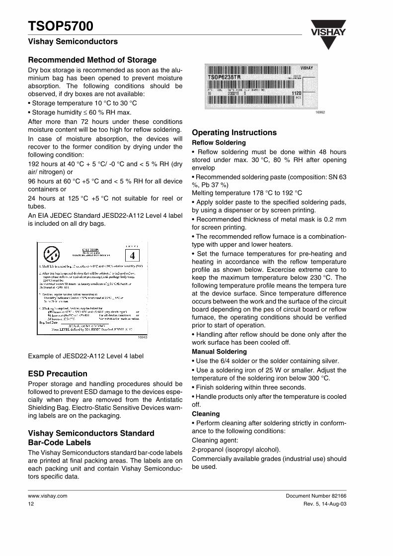
Recommended Method of StorageDry box storage is recommended as soon as the alu-minium bag has been opened to prevent moistureabsorption. The following conditions should beobserved, if dry boxes are not available:• Storage temperature 10 °C to 30 °C• Storage humidity ≤ 60 % RH max.After more than 72 hours under these conditionsmoisture content will be too high for reflow soldering.In case of moisture absorption, the devices willrecover to the former condition by drying under thefollowing condition:192 hours at 40 °C + 5 °C/ -0 °C and < 5 % RH (dryair/ nitrogen) or96 hours at 60 °C +5 °C and < 5 % RH for all devicecontainers or24 hours at 125 °C +5 °C not suitable for reel ortubes.An EIA JEDEC Standard JESD22-A112 Level 4 labelis included on all dry bags.
Example of JESD22-A112 Level 4 label
ESD PrecautionProper storage and handling procedures should befollowed to prevent ESD damage to the devices espe-cially when they are removed from the AntistaticShielding Bag. Electro-Static Sensitive Devices warn-ing labels are on the packaging.
Vishay Semiconductors StandardBar-Code LabelsThe Vishay Semiconductors standard bar-code labelsare printed at final packing areas. The labels are oneach packing unit and contain Vishay Semiconduc-tors specific data.
Operating InstructionsReflow Soldering• Reflow soldering must be done within 48 hoursstored under max. 30 °C, 80 % RH after openingenvelop• Recommended soldering paste (composition: SN 63%, Pb 37 %)Melting temperature 178 °C to 192 °C• Apply solder paste to the specified soldering pads,by using a dispenser or by screen printing.• Recommended thickness of metal mask is 0.2 mmfor screen printing.• The recommended reflow furnace is a combination-type with upper and lower heaters.• Set the furnace temperatures for pre-heating andheating in accordance with the reflow temperatureprofile as shown below. Excercise extreme care tokeep the maximum temperature below 230 °C. Thefollowing temperature profile means the tempera tureat the device surface. Since temperature differenceoccurs between the work and the surface of the circuitboard depending on the pes of circuit board or reflowfurnace, the operating conditions should be verifiedprior to start of operation.• Handling after reflow should be done only after thework surface has been cooled off.Manual Soldering• Use the 6/4 solder or the solder containing silver.• Use a soldering iron of 25 W or smaller. Adjust thetemperature of the soldering iron below 300 °C.• Finish soldering within three seconds.• Handle products only after the temperature is cooledoff.Cleaning• Perform cleaning after soldering strictly in conform-ance to the following conditions:Cleaning agent:2-propanol (isopropyl alcohol).Commercially available grades (industrial use) shouldbe used.
16943
16962
www.vishay.com
12
Document Number 82166
Rev. 5, 14-Aug-03
VISHAY TSOP5700Vishay Semiconductors
Demineralized or distilled water having a resistivity ofnot less than 500 mΩ corresponding to a conductivityof 2 mS/m.• Temperature and time: 30 seconds under the tem-perature below 50 °C or 3 minutes below 30 °C.• Ultrasonic cleaning: Below 20 W.
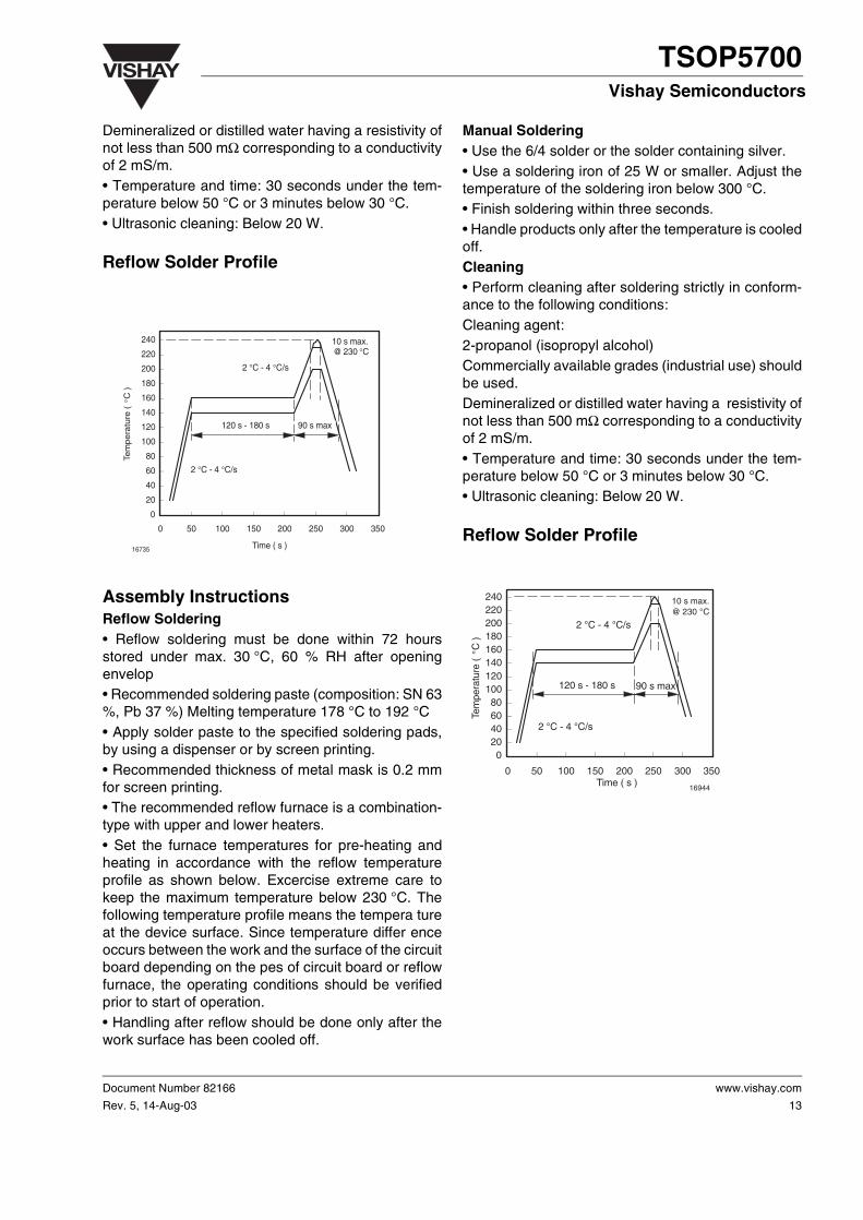
Reflow Solder Profile
Assembly InstructionsReflow Soldering• Reflow soldering must be done within 72 hoursstored under max. 30 °C, 60 % RH after openingenvelop• Recommended soldering paste (composition: SN 63%, Pb 37 %) Melting temperature 178 °C to 192 °C• Apply solder paste to the specified soldering pads,by using a dispenser or by screen printing.• Recommended thickness of metal mask is 0.2 mmfor screen printing.• The recommended reflow furnace is a combination-type with upper and lower heaters.• Set the furnace temperatures for pre-heating andheating in accordance with the reflow temperatureprofile as shown below. Excercise extreme care tokeep the maximum temperature below 230 °C. Thefollowing temperature profile means the tempera tureat the device surface. Since temperature differ enceoccurs between the work and the surface of the circuitboard depending on the pes of circuit board or reflowfurnace, the operating conditions should be verifiedprior to start of operation.• Handling after reflow should be done only after thework surface has been cooled off.
Manual Soldering• Use the 6/4 solder or the solder containing silver.• Use a soldering iron of 25 W or smaller. Adjust thetemperature of the soldering iron below 300 °C.• Finish soldering within three seconds.• Handle products only after the temperature is cooledoff.Cleaning• Perform cleaning after soldering strictly in conform-ance to the following conditions:Cleaning agent:2-propanol (isopropyl alcohol)Commercially available grades (industrial use) shouldbe used.Demineralized or distilled water having a resistivity ofnot less than 500 mΩ corresponding to a conductivityof 2 mS/m.• Temperature and time: 30 seconds under the tem-perature below 50 °C or 3 minutes below 30 °C.• Ultrasonic cleaning: Below 20 W.
Reflow Solder Profile0
20
40
60
80
100
120
140
160
180
200
220
240
0 50 100 150 200 250 300 350
Time ( s )
Tem
pera
ture
(C
)
16735
°
2 °C - 4 °C/s
10 s max.@ 230 °C
90 s max120 s - 180 s
2 °C - 4 °C/s
10 s max.@ 230 C
90 s max
020406080
100120140160180200220240
0 50 100 150 200 250 300 350Time ( s )
Tem
pera
ture
(
C )
16944
2 C - 4 C/s
120 s - 180 s
2 C - 4 C/s
Document Number 82166
Rev. 5, 14-Aug-03
www.vishay.com
13

VISHAYTSOP5700Vishay Semiconductors
Taping Version TSOP..TT
www.vishay.com
14
Document Number 82166
Rev. 5, 14-Aug-03

VISHAY TSOP5700Vishay Semiconductors
Taping Version TSOP..TR
Document Number 82166
Rev. 5, 14-Aug-03
www.vishay.com
15

VISHAYTSOP5700Vishay Semiconductors
Reel Dimensions
www.vishay.com
16
Document Number 82166
Rev. 5, 14-Aug-03

VISHAY TSOP5700Vishay Semiconductors
Leader and Trailer
Cover Tape Peel StrengthAccording to DIN EN 60286-30.1 to 1.3 N300 ± 10 mm/min165 ° - 180 ° peel angle
LabelStandard bar code labels for finished goodsThe standard bar code labels are product labels andused for identification of goods. The finished goodsare packed in final packing area. The standard pack-ing units are labeled with standard bar code labelsbefore transported as finished goods to warehouses.The labels are on each packing unit and containVishay Semiconductor GmbH specific data.
Dry PackingThe reel is packed in an anti-humidity bag to protectthe devices from absorbing moisture during transpor-tation and storage.
Final PackingThe sealed reel is packed into a cardboard box. Asecondary cardboard box is used for shipping pur-poses.
Document Number 82166
Rev. 5, 14-Aug-03
www.vishay.com
17

VISHAYTSOP5700Vishay Semiconductors
Recommended Method of StorageDry box storage is recommended as soon as the alu-minium bag has been opened to prevent moistureabsorption. The following conditions should beobserved, if dry boxes are not available:• Storage temperature 10 °C to 30 °C• Storage humidity ≤ 60 % RH max.After more than 72 hours under these conditionsmoisture content will be too high for reflow soldering.In case of moisture absorption, the devices willrecover to the former condition by drying under thefollowing condition:192 hours at 40 °C + 5 °C/ -0 °C and < 5 % RH (dryair/ nitrogen) or96 hours at 60 °C +5 °C and < 5 % RH for all devicecontainers or24 hours at 125 °C +5 °C not suitable for reel ortubes.An EIA JEDEC Standard JESD22-A112 Level 4 labelis included on all dry bags.Example of JESD22-A112 Level 4 label
ESD PrecautionProper storage and handling procedures should befollowed to prevent ESD damage to the devices espe-cially when they are removed from the AntistaticShielding Bag. Electro-Static Sensitive Devices warn-ing labels are on the packaging.
Vishay Semiconductors StandardBar-Code LabelsThe Vishay Semiconductors standard bar-code labelsare printed at final packing areas. The labels are oneach packing unit and contain Vishay Telefunkenspecific data.
www.vishay.com
18
Document Number 82166
Rev. 5, 14-Aug-03

VISHAY TSOP5700Vishay Semiconductors
Ozone Depleting Substances Policy Statement
It is the policy of Vishay Semiconductor GmbH to
1. Meet all present and future national and international statutory requirements.
2. Regularly and continuously improve the performance of our products, processes, distribution and operatingsystems with respect to their impact on the health and safety of our employees and the public, as well as their impact on the environment.
It is particular concern to control or eliminate releases of those substances into the atmosphere which are known as ozone depleting substances (ODSs).
The Montreal Protocol (1987) and its London Amendments (1990) intend to severely restrict the use of ODSs and forbid their use within the next ten years. Various national and international initiatives are pressing for an earlier ban on these substances.
Vishay Semiconductor GmbH has been able to use its policy of continuous improvements to eliminate the use of ODSs listed in the following documents.
1. Annex A, B and list of transitional substances of the Montreal Protocol and the London Amendments respectively
2. Class I and II ozone depleting substances in the Clean Air Act Amendments of 1990 by the Environmental Protection Agency (EPA) in the USA
3. Council Decision 88/540/EEC and 91/690/EEC Annex A, B and C (transitional substances) respectively.
Vishay Semiconductor GmbH can certify that our semiconductors are not manufactured with ozone depleting substances and do not contain such substances.
We reserve the right to make changes to improve technical design and may do so without further notice.
Parameters can vary in different applications. All operating parameters must be validated for each customer application by the customer. Should the buyer use Vishay Semiconductors products for any unintended or unauthorized application, the buyer shall indemnify Vishay Semiconductors against all
claims, costs, damages, and expenses, arising out of, directly or indirectly, any claim of personal damage, injury or death associated with such unintended or unauthorized use.
Vishay Semiconductor GmbH, P.O.B. 3535, D-74025 Heilbronn, GermanyTelephone: 49 (0)7131 67 2831, Fax number: 49 (0)7131 67 2423
Document Number 82166
Rev. 5, 14-Aug-03
www.vishay.com
19